sifive e300 platform reference manual · 2 sifive e300 platform reference manual, version 1.0.1...
TRANSCRIPT

SiFive E300 Platform Reference Manual
Version 1.0.1c© SiFive, Inc.

2 SiFive E300 Platform Reference Manual, Version 1.0.1
SiFive E300 Platform Reference Manual
Proprietary NoticeCopyright c© 2016, SiFive Inc. All rights reserved.
Information in this document is provided “as is”, with all faults.
SiFive expressly disclaims all warranties, representations and conditions of any kind, whether ex-press or implied, including, but not limited to, the implied warranties or conditions of merchantabil-ity, fitness for a particular purpose and non-infringement.
SiFive does not assume any liability rising out of the application or use of any product or circuit, andspecifically disclaims any and all liability, including without limitation indirect, incidental, special,exemplary, or consequential damages.
SiFive reserves the right to make changes without further notice to any products herein.
Release Information
Version Date Changes1.0.1 Dec 19, 2016 Minor clarifications on PWM, SPI, AON register fields1.0 November 29, 2016 Initial release for HiFive1 release.
i

ii SiFive E300 Platform Reference Manual, Version 1.0.1
Contents
SiFive E300 Platform Reference Manual i
1 Introduction 1
1.1 Block Diagram . . . . . . . . . . . . . . . . . . . . . . . . . . . . . . . . . . . . . . . . . . 1
1.2 Configurable E31 RISC-V Coreplex . . . . . . . . . . . . . . . . . . . . . . . . . . . . . . 1
1.3 Custom Accelerators . . . . . . . . . . . . . . . . . . . . . . . . . . . . . . . . . . . . . . . 2
1.4 On-Chip Memory . . . . . . . . . . . . . . . . . . . . . . . . . . . . . . . . . . . . . . . . . 2
1.5 Execute-in-Place Quad-SPI Flash controller . . . . . . . . . . . . . . . . . . . . . . . . . . 2
1.6 Peripheral Devices . . . . . . . . . . . . . . . . . . . . . . . . . . . . . . . . . . . . . . . . 3
1.7 Platform-Level Interrupt Controller . . . . . . . . . . . . . . . . . . . . . . . . . . . . . . . 3
1.8 Always-On Block and Power Management . . . . . . . . . . . . . . . . . . . . . . . . . . . 3
1.9 Debug Support . . . . . . . . . . . . . . . . . . . . . . . . . . . . . . . . . . . . . . . . . . 3
1.10 Software Tools . . . . . . . . . . . . . . . . . . . . . . . . . . . . . . . . . . . . . . . . . . 3
2 E300 Platform Memory Map 5
3 E300 Power Modes 7
3.1 Run Mode . . . . . . . . . . . . . . . . . . . . . . . . . . . . . . . . . . . . . . . . . . . . . 7
3.2 Wait Mode . . . . . . . . . . . . . . . . . . . . . . . . . . . . . . . . . . . . . . . . . . . . 7
3.3 Sleep Mode . . . . . . . . . . . . . . . . . . . . . . . . . . . . . . . . . . . . . . . . . . . . 7
4 E300 Clock Generation 9
4.1 Clock Generation Overview . . . . . . . . . . . . . . . . . . . . . . . . . . . . . . . . . . . 9
4.2 Internal Trimmable Programmable 72 MHz Oscillator (HFROSC) . . . . . . . . . . . . . . 9
4.3 External 16 MHz Crystal Oscillator (HFXOSC) . . . . . . . . . . . . . . . . . . . . . . . . 11
4.4 Internal High-Frequency PLL (HFPLL) . . . . . . . . . . . . . . . . . . . . . . . . . . . . . 11
4.5 PLL Output Divider . . . . . . . . . . . . . . . . . . . . . . . . . . . . . . . . . . . . . . . . 13
4.6 Internal Low-Frequency Oscillator (LFRCOSC) . . . . . . . . . . . . . . . . . . . . . . . . 13
4.7 External 32.768 kHz Low-Frequency Crystal Oscillator (LFXOSC) . . . . . . . . . . . . . 13
iii

iv SiFive E300 Platform Reference Manual, Version 1.0.1
5 E300 Always-On (AON) Domain 15
5.1 AON Power Source . . . . . . . . . . . . . . . . . . . . . . . . . . . . . . . . . . . . . . . 15
5.2 AON Clocking and Tilelink Slave Port . . . . . . . . . . . . . . . . . . . . . . . . . . . . . 15
5.3 AON Reset Unit . . . . . . . . . . . . . . . . . . . . . . . . . . . . . . . . . . . . . . . . . 15
5.3.1 Power-On Reset Circuit . . . . . . . . . . . . . . . . . . . . . . . . . . . . . . . 16
5.3.2 External Reset Circuit . . . . . . . . . . . . . . . . . . . . . . . . . . . . . . . . 16
5.3.3 Reset Cause . . . . . . . . . . . . . . . . . . . . . . . . . . . . . . . . . . . . . 17
5.4 Watchdog Timer (WDT) . . . . . . . . . . . . . . . . . . . . . . . . . . . . . . . . . . . . . 17
5.5 Real-Time Clock (RTC) . . . . . . . . . . . . . . . . . . . . . . . . . . . . . . . . . . . . . 17
5.6 Backup Registers . . . . . . . . . . . . . . . . . . . . . . . . . . . . . . . . . . . . . . . . 17
5.7 Power-Management Unit (PMU) . . . . . . . . . . . . . . . . . . . . . . . . . . . . . . . . 17
5.8 AON Memory Map . . . . . . . . . . . . . . . . . . . . . . . . . . . . . . . . . . . . . . . . 17
6 E300 Power-Management Unit (PMU) 19
6.1 PMU Overview . . . . . . . . . . . . . . . . . . . . . . . . . . . . . . . . . . . . . . . . . . 19
6.2 PMU Key Register (pmukey) . . . . . . . . . . . . . . . . . . . . . . . . . . . . . . . . . . . 19
6.3 PMU Program . . . . . . . . . . . . . . . . . . . . . . . . . . . . . . . . . . . . . . . . . . 19
6.4 Initiate Sleep Sequence Register (pmusleep) . . . . . . . . . . . . . . . . . . . . . . . . . 20
6.5 Wakeup Signal Conditioning . . . . . . . . . . . . . . . . . . . . . . . . . . . . . . . . . . 21
6.6 PMU Interrupt Enables (pmuie) and Wakeup Cause (pmucause) . . . . . . . . . . . . . . . 21
6.7 Memory Map . . . . . . . . . . . . . . . . . . . . . . . . . . . . . . . . . . . . . . . . . . . 22
7 E300 Power, Reset, Clock, Interrupt (PRCI) Control and Status Registers 23
7.1 PRCI Address Space Usage . . . . . . . . . . . . . . . . . . . . . . . . . . . . . . . . . . 23
8 E300 Watchdog Timer (WDT) 25
8.1 Watchdog Count Register (wdogcount) . . . . . . . . . . . . . . . . . . . . . . . . . . . . . 25
8.2 Watchdog Clock Selection . . . . . . . . . . . . . . . . . . . . . . . . . . . . . . . . . . . . 26
8.3 Watchdog Configuration Register wdogcfg . . . . . . . . . . . . . . . . . . . . . . . . . . . 26
8.4 Watchdog Compare Register (wdogcmp) . . . . . . . . . . . . . . . . . . . . . . . . . . . . 27
8.5 Watchdog Key Register (wdogkey) . . . . . . . . . . . . . . . . . . . . . . . . . . . . . . . 27
8.6 Watchdog Feed Address (wdogfeed) . . . . . . . . . . . . . . . . . . . . . . . . . . . . . . 27
8.7 Watchdog Configuration . . . . . . . . . . . . . . . . . . . . . . . . . . . . . . . . . . . . . 27
8.8 Watchdog Resets . . . . . . . . . . . . . . . . . . . . . . . . . . . . . . . . . . . . . . . . 27
8.9 Watchdog Interrupts (wdogcmpip) . . . . . . . . . . . . . . . . . . . . . . . . . . . . . . . . 28
9 E300 Real-Time Clock (RTC) 29
9.1 RTC Count Registers rtchi/rtclo . . . . . . . . . . . . . . . . . . . . . . . . . . . . . . . 29

Copyright c© 2016, SiFive Inc. All rights reserved. v
9.2 RTC Configuration Register rtccfg . . . . . . . . . . . . . . . . . . . . . . . . . . . . . . 29
9.3 RTC Compare Register rtccmp . . . . . . . . . . . . . . . . . . . . . . . . . . . . . . . . . 30
10 E300 Backup Registers 31
11 General Purpose Input/Output Controller (GPIO) 33
11.1 Memory Map . . . . . . . . . . . . . . . . . . . . . . . . . . . . . . . . . . . . . . . . . . . 33
11.2 Input / Output Values . . . . . . . . . . . . . . . . . . . . . . . . . . . . . . . . . . . . . . 33
11.3 Interrupts . . . . . . . . . . . . . . . . . . . . . . . . . . . . . . . . . . . . . . . . . . . . . 33
11.4 Internal Pull-Ups . . . . . . . . . . . . . . . . . . . . . . . . . . . . . . . . . . . . . . . . . 35
11.5 Drive Strength . . . . . . . . . . . . . . . . . . . . . . . . . . . . . . . . . . . . . . . . . . 35
11.6 Output Inversion . . . . . . . . . . . . . . . . . . . . . . . . . . . . . . . . . . . . . . . . . 35
11.7 HW I/O Functions (IOF) . . . . . . . . . . . . . . . . . . . . . . . . . . . . . . . . . . . . . 35
11.8 Behavior During Sleep Mode . . . . . . . . . . . . . . . . . . . . . . . . . . . . . . . . . . 36
12 Universal Asynchronous Receiver/Transmitter (UART) 37
12.1 UART Overview . . . . . . . . . . . . . . . . . . . . . . . . . . . . . . . . . . . . . . . . . 37
12.2 Memory Map . . . . . . . . . . . . . . . . . . . . . . . . . . . . . . . . . . . . . . . . . . . 37
12.3 Transmit Data Register (txdata) . . . . . . . . . . . . . . . . . . . . . . . . . . . . . . . . 38
12.4 Receive Data Register (rxdata) . . . . . . . . . . . . . . . . . . . . . . . . . . . . . . . . 38
12.5 Transmit Control Register (txctrl) . . . . . . . . . . . . . . . . . . . . . . . . . . . . . . . 38
12.6 Receive Control Register (rxctrl) . . . . . . . . . . . . . . . . . . . . . . . . . . . . . . . 39
12.7 Interrupt Registers (ip and ie) . . . . . . . . . . . . . . . . . . . . . . . . . . . . . . . . . 39
12.8 Baud Rate Divisor Register (div) . . . . . . . . . . . . . . . . . . . . . . . . . . . . . . . . 39
13 Serial Peripheral Interface (SPI) 41
13.1 SPI Overview . . . . . . . . . . . . . . . . . . . . . . . . . . . . . . . . . . . . . . . . . . . 41
13.2 Memory Map . . . . . . . . . . . . . . . . . . . . . . . . . . . . . . . . . . . . . . . . . . . 41
13.3 Serial Clock Divisor Register (sckdiv) . . . . . . . . . . . . . . . . . . . . . . . . . . . . . 41
13.4 Serial Clock Mode Register (sckmode) . . . . . . . . . . . . . . . . . . . . . . . . . . . . . 42
13.5 Chip Select ID Register (csid) . . . . . . . . . . . . . . . . . . . . . . . . . . . . . . . . . 43
13.6 Chip Select Default Register (csdef) . . . . . . . . . . . . . . . . . . . . . . . . . . . . . . 43
13.7 Chip Select Mode Register (csmode) . . . . . . . . . . . . . . . . . . . . . . . . . . . . . . 43
13.8 Delay Control Registers (delay0 and delay1) . . . . . . . . . . . . . . . . . . . . . . . . . 44
13.9 Frame Format Register (fmt) . . . . . . . . . . . . . . . . . . . . . . . . . . . . . . . . . . 44
13.10 Transmit Data Register (txdata) . . . . . . . . . . . . . . . . . . . . . . . . . . . . . . . . 45
13.11 Receive Data Register (rxdata) . . . . . . . . . . . . . . . . . . . . . . . . . . . . . . . . 45
13.12 Transmit Watermark Register (txmark) . . . . . . . . . . . . . . . . . . . . . . . . . . . . . 46

vi SiFive E300 Platform Reference Manual, Version 1.0.1
13.13 Receive Watermark Register (rxmark) . . . . . . . . . . . . . . . . . . . . . . . . . . . . . 46
13.14 Interrupt Registers (ie and ip) . . . . . . . . . . . . . . . . . . . . . . . . . . . . . . . . . 46
13.15 SPI Flash Interface Control Register (fctrl) . . . . . . . . . . . . . . . . . . . . . . . . . 47
13.16 SPI Flash Instruction Format Register (ffmt) . . . . . . . . . . . . . . . . . . . . . . . . . 47
14 One-Time Programmable Memory (OTP) Peripheral 49
14.1 Memory Map . . . . . . . . . . . . . . . . . . . . . . . . . . . . . . . . . . . . . . . . . . . 49
14.2 Programmed-I/O lock register (otp lock) . . . . . . . . . . . . . . . . . . . . . . . . . . . 49
14.3 Programmed-I/O Sequencing . . . . . . . . . . . . . . . . . . . . . . . . . . . . . . . . . . 51
14.4 Read sequencer control register (otp rsctrl) . . . . . . . . . . . . . . . . . . . . . . . . 51
15 E300 Pulse-Width Modulation (PWM) Peripheral 53
15.1 PWM Overview . . . . . . . . . . . . . . . . . . . . . . . . . . . . . . . . . . . . . . . . . . 53
15.2 PWM Memory Map . . . . . . . . . . . . . . . . . . . . . . . . . . . . . . . . . . . . . . . 53
15.3 PWM Count Register (pwmcount) . . . . . . . . . . . . . . . . . . . . . . . . . . . . . . . . 53
15.4 PWM Configuration Register (pwmcfg) . . . . . . . . . . . . . . . . . . . . . . . . . . . . . 54
15.5 PWM Compare Registers (pwmcmp0–pwmcmp3) . . . . . . . . . . . . . . . . . . . . . . . . . 55
15.6 Deglitch and Sticky circuitry . . . . . . . . . . . . . . . . . . . . . . . . . . . . . . . . . . . 56
15.7 Generating Left- or Right-Aligned PWM Waveforms . . . . . . . . . . . . . . . . . . . . . 56
15.8 Generating Center-Aligned (Phase-Correct) PWM Waveforms . . . . . . . . . . . . . . . 57
15.9 Generating Arbitrary PWM Waveforms using Ganging . . . . . . . . . . . . . . . . . . . . 58
15.10 Generating One-shot Waveforms . . . . . . . . . . . . . . . . . . . . . . . . . . . . . . . . 58
15.11 PWM Interrupts . . . . . . . . . . . . . . . . . . . . . . . . . . . . . . . . . . . . . . . . . . 58

Chapter 1
Introduction
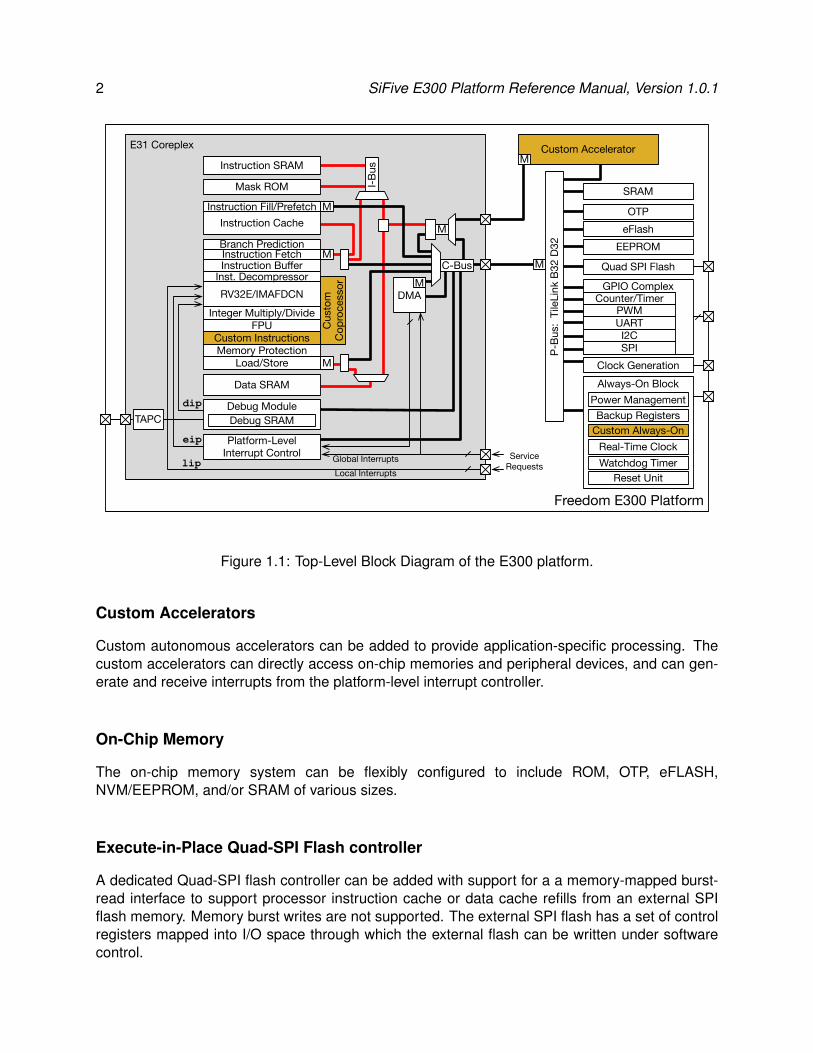
The E300 platform is the first member of SiFive’s Freedom Everywhere family of customizableRISC-V SoCs. By combining a highly configurable base platform with customer-specific hardwareextensions, the Freedom Everywhere family provides low-NRE and rapid time-to-market solutionsfor performance, cost, and power-sensitive embedded and IoT markets.
Each E300 SoC includes a SiFive E3 series RISC-V Coreplex with integrated instruction and datamemories, a platform-level interrupt controller, on-chip debug unit, and an extensive selection ofperipheral devices. This manual should be read together with the E3 Coreplex manual.
All aspects of the base E300 platform can be flexibly configured. In addition, the platform can bereadily extended with customer-specific instruction-set extensions, custom coprocessors, customaccelerators, custom I/O, and custom always-on blocks. The resulting application-specific E300SoC is optimized for manufacture in a TSMC 180nm process, and delivered as packaged testedparts by SiFive.
Block DiagramFigure 1.1 shows the top-level block diagram of the E300 platform. The heart of the currentE300 platform is an E31 Coreplex, which contains an E31 RISC-V processor, instruction and datamemories, the platform-level interrupt controller (PLIC), a central DMA controller, and a debugmodule.
Configurable E31 RISC-V CoreplexThe configurable E31 RISC-V Coreplex provides a high-performance single-issue in-order 32-bitexecution pipeline, with a peak sustained execution rate of one instruction per clock cycle. TheFreedom E300 platform supports most configuration options of the E31 core as described in theE3 Coreplex manual, except for the following:
• Where present, the instruction cache line size is 32 bytes.
• The data cache is not supported.
The E3 Coreplex exports two TileLink attachments; a TileLink master port which can be used toattach a custom accelerator, and a TileLink slave port to drive the platform bus. Both ports support32-byte burst accesses over a 32-bit datapath.
1
2 SiFive E300 Platform Reference Manual, Version 1.0.1
Freedom E300 Platform
Clock Generation
P-Bu
s: T
ileLi
nk B
32 D
32
eFlash
E31 Coreplex
Platform-Level Interrupt Control
TAPCDebug ModuleDebug SRAM
Instruction Fetch
RV32E/IMAFDCN
Branch Prediction
Integer Multiply/Divide
Inst. Decompressor
Memory ProtectionCustom Instructions
Cust
om
Copr
oces
sor
Instruction BufferM
MLoad/Store
dip
eip
lip
DMAM
M
C-Bus
Instruction CacheInstruction Fill/Prefetch M
Instruction SRAM
Mask ROM
Data SRAMI-B
us
Quad SPI Flash
Custom AcceleratorM
M
Local InterruptsGlobal Interrupts
EEPROM
Service Requests
Always-On Block
Backup Registers
Real-Time ClockCustom Always-On
Reset UnitWatchdog Timer
GPIO Complex
PWMCounter/Timer
UARTI2CSPI
SRAM
OTP
FPU
Power Management
Figure 1.1: Top-Level Block Diagram of the E300 platform.
Custom Accelerators
Custom autonomous accelerators can be added to provide application-specific processing. Thecustom accelerators can directly access on-chip memories and peripheral devices, and can gen-erate and receive interrupts from the platform-level interrupt controller.
On-Chip Memory
The on-chip memory system can be flexibly configured to include ROM, OTP, eFLASH,NVM/EEPROM, and/or SRAM of various sizes.
Execute-in-Place Quad-SPI Flash controller
A dedicated Quad-SPI flash controller can be added with support for a a memory-mapped burst-read interface to support processor instruction cache or data cache refills from an external SPIflash memory. Memory burst writes are not supported. The external SPI flash has a set of controlregisters mapped into I/O space through which the external flash can be written under softwarecontrol.
Copyright c© 2016, SiFive Inc. All rights reserved. 3
Peripheral DevicesPeripheral devices can be selected from a large catalog of standard components, includingcounter/timers, watchdogs, PWM, GPIO, UART, I2C, SPI, ADC, DAC, SD/eMMC, USB 1.1/2.0OTG, and 10/100/1000 Ethernet. The autonomous Coreplex DMA engine can be added to reduceprocessor overhead in servicing I/O transfers to and from data memory. Third-party peripheral IPcan be attached via industry-standard SoC buses or TileLink. Please contact SiFive for details onthe available peripheral offerings, or on how to connect to existing IP.
Platform-Level Interrupt ControllerThe configurable platform-level interrupt controller (PLIC) supports a large number of inputs andprogrammable priority levels, and with the addition of the N extension can also support nestedinterrupt handling for fast interrupt response.
Always-On Block and Power ManagementE300 SoCs can be configured with active power management to reduce leakage current in sleepmode. The Always-On Block (AON) supports low-power sleep with wakeup from an internal real-time clock interrupt or external I/O stimulus, or custom always-on circuitry.
Debug SupportEach E300 system includes extensive platform-level debug facilities including hardware break-points, watchpoints, and single-step execution accessed via an industry-standard JTAG interfaceand supported by a full set of open-source debug tools. All components in the system, includ-ing the processor, accelerators, memories, peripheral devices, and interrupt controller, can becontrolled and monitored over the debug port.
Software ToolsSiFive provides a full open-source RISC-V embedded software development toolchain for E300SoCs, including modern C and C++ compilers with soft-floating-point support, standard libraries,assemblers, linkers, and the FreeRTOS real-time operating system, together with debug tools todrive the on-chip debug hardware.

4 SiFive E300 Platform Reference Manual, Version 1.0.1

Chapter 2
E300 Platform Memory Map
The overall memory map of E300 is shown in Table 2.1.
Base Top Description0x0000 0000 0x0FFF FFFF (see E3 Coreplex Manual) E3 Coreplex (256 MiB)0x1000 0000 0x1000 7FFF Always-On (AON) (≤32 KiB)
Off-Coreplex I/O (1.75 GiB)
0x1000 8000 0x1000 FFFF Power, Reset, Clock, Interrupts (PRCI)(≤32 KiB)
0x1001 0000 0x1001 0FFF On-chip OTP control0x1001 1000 0x1001 1FFF On-chip eFlash control0x1001 2000 0x1001 2FFF GPIO00x1001 3000 0x1001 3FFF UART00x1001 4000 0x1001 4FFF QSPI00x1001 5000 0x1FFF FFFF Additional Peripherals (<256MiB)0x2000 0000 0x3FFF FFFF Off-chip QSPI0 flash read (512 MiB)0x4000 0000 0x7FFF FFFF Additional I/O or RAM (1 GiB)0x8000 0000 0x8001 FFFF Instruction and Data RAM (≤ 128 KiB)
Memory (2 GiB)0x8002 0000 0xFFFF FFFF Additional RAM
Table 2.1: E300 Physical Memory Map.
5

6 SiFive E300 Platform Reference Manual, Version 1.0.1

Chapter 3
E300 Power Modes
This chapter describes the different power modes available on E300 systems. E300 systemscurrently support three power modes: Run, Wait, and Sleep.
Run ModeRun mode corresponds to regular execution where the processor is running. Power consumptioncan be adjusted by varying the clock frequency of the processor and peripheral bus, and by en-abling or disabling individual peripheral blocks. The processor exits run mode by executing a “Waitfor Interrupt” (WFI) instruction.
Wait ModeWhen the processor executes a WFI instruction it enters Wait mode, which halts instruction exe-cution and gates the clocks driving the processor pipeline. All state is preserved in the system.The processor will resume in Run mode when there is a local interrupt pending or when the PLICsends an interrupt notification. The processor may also exit wait mode for other events, and soft-ware must check system status when exiting wait mode to determine the correct course of action.
Sleep ModeSleep mode is entered by writing to a memory-mapped register pmusleep in the power-management unit (PMU). The pmusleep register is protected by the pmukey register which mustbe written with a defined value before writing to pmusleep.
The PMU will then execute a power-down sequence to turn off power to the processor and mainpads. All volatile state in the system is lost except for state held in the AON domain. The mainoutput pads will be left floating.
Sleep mode is exited when an enabled wakeup event occurs, whereupon the PMU will initiatea wakeup sequence. The wakeup sequence turns on the core and pad power supplies whileasserting reset on the clocks, core and pads. After the power supplies stabilize, the clock resetis deasserted to allow the clocks to stabilize. Once the clocks are stable, the pad and processorresets are deasserted, and the processor begins running from the reset vector.
Software must reinitialize the core and can interrogate the PMU pmucause register to determinethe cause of reset, and can recover pre-sleep state from the backup registers. The processor
7

8 SiFive E300 Platform Reference Manual, Version 1.0.1
always initially runs from the HFROSC at the default setting, and must reconfigure clocks to runfrom an alternate clock source (HFXOSC or PLL) or at a different setting on the HFROSC.

Chapter 4
E300 Clock Generation
The Freedom E300 platform supports many alternative clock-generation schemes to match appli-cation needs. This chapter describes the basic structure of E300 clock generation. The variousclock configuration registers live either in the AON block (Chapter 5) or the PRCI block (Chapter 7).
Clock Generation Overview
Optional PLL
Optional HF crystal oscillator
Optional LF RC oscillator
Optional LF crystal oscillator
Optional peripherals
Always-On Domain
pllref pllout6-48MHz 50-400MHzPLL
JTAG tck ≤16MHz
hfroscout1.125-72MHz
lfxoscin
lfxoscout
32.768kHz
hfxoscin
hfxoscout16MHz
LFRCOSClfrcoscout
30-60kHz
pllcfg
jtagclk
÷N
plloutdiv
coreclk
÷N
spiclkcfg
spiclk
8/16*baud rate÷N
uartclkcfg
uartclk
25MHz/125MHz÷N
enetclkcfg
enetclk
÷N
usbclkcfg
usbclk60MHz
hfclk
÷N
hyperclkcfg
hyperclk≤ 166MHz
÷N
i2sclkcfg
i2sclk1.536MHz/1.4112MHz
pllrefsel
1
0
jtagclk is selected when psdscanen is asserted
HFROSC
hfrosccfg
÷Npllsel
0
1
Real-Time Clock/Alarm
Watchdog Timer
psdclkbypass_n
1
0
LFROSC
lfrosccfg
÷N
÷4
psdhfclkout
psdlfclkout
Only one on-chip
LFxOSC in system
tlclk
Process Monitor ÷N
procmoncfg
3
0
psdlfaltclkpsdlfclksel
10
12
hfxosccfg
psdscanen_n psdscanen
0.4-400MHz
Figure 4.1: E300 clock generation scheme.
9
10 SiFive E300 Platform Reference Manual, Version 1.0.1
Figure 4.1 shows an overview of the E300 clock generation scheme. Most digital clocks on thechip are divided down from a central high-frequency clock hfclk produced from either the PLL oran on-chip trimmable oscillator. The PLL can be driven from either the on-chip oscillator or an off-chip crystal oscillator. In systems without a PLL, the off-chip oscillator can drive the high-frequencyclock directly.
For the FE310-G000, the TileLink bus clock (tlclk) is fixed to be the same as the processor coreclock (coreclk). As shown, each peripheral may also generate local divided clocks from tlclk.
The Always-On block includes a real-time clock circuit that is driven from one of three possiblelow-frequency clock sources: an off-chip 32 kHz crystal oscillator, an on-chip low-frequency RCoscillator, or a clock divided down from hfclk.
Test mode can select the JTAG test clk (TCK) to be driven into all clock trees to support scan.
Internal Trimmable Programmable 72 MHz Oscillator (HFROSC)
An internal trimmable high-frequency ring oscillator (HFROSC) is used to provide the default clockafter reset, and can be used to allow operation without an external high-frequency crystal or aPLL.
The oscillator is controlled by the hfrosccfg register, which is memory-mapped in the PRCI ad-dress space, and whose format is shown in Figure 4.1.
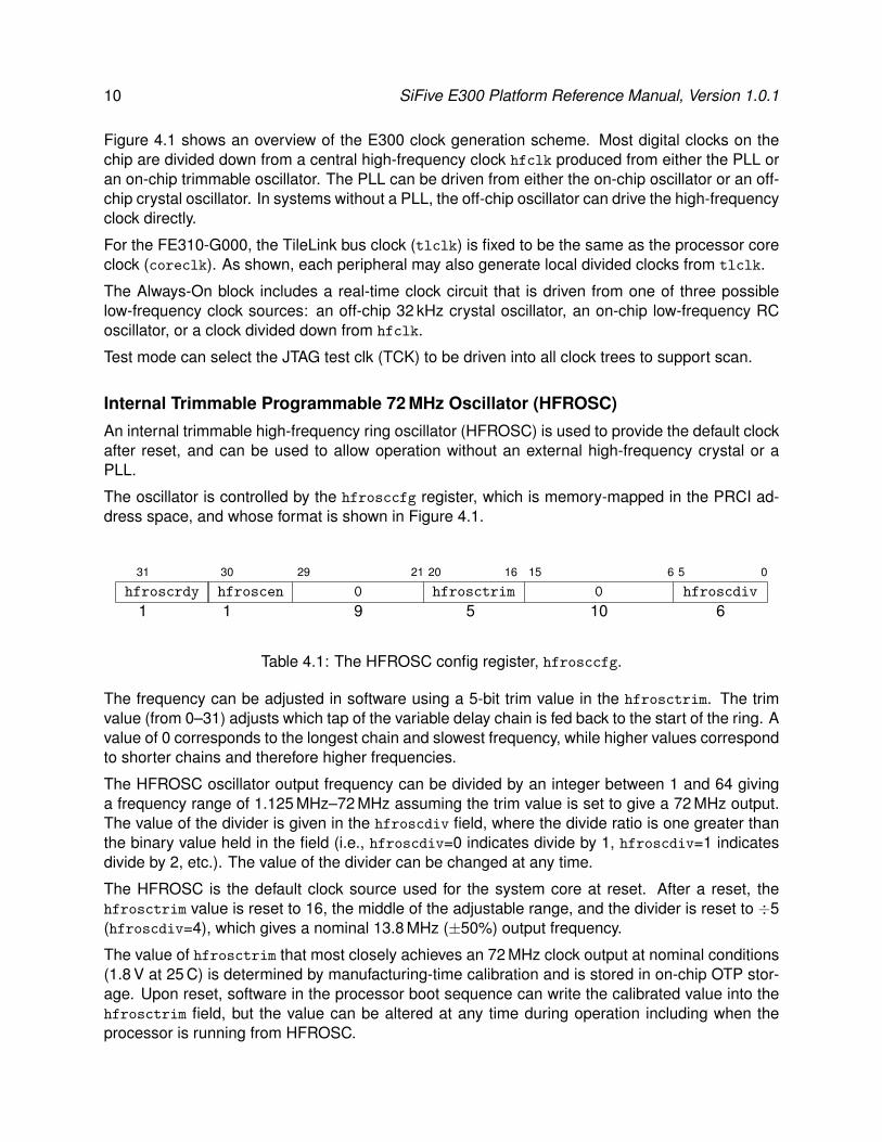
31 30 29 21 20 16 15 6 5 0
hfroscrdy hfroscen 0 hfrosctrim 0 hfroscdiv
1 1 9 5 10 6
Table 4.1: The HFROSC config register, hfrosccfg.
The frequency can be adjusted in software using a 5-bit trim value in the hfrosctrim. The trimvalue (from 0–31) adjusts which tap of the variable delay chain is fed back to the start of the ring. Avalue of 0 corresponds to the longest chain and slowest frequency, while higher values correspondto shorter chains and therefore higher frequencies.
The HFROSC oscillator output frequency can be divided by an integer between 1 and 64 givinga frequency range of 1.125 MHz–72 MHz assuming the trim value is set to give a 72 MHz output.The value of the divider is given in the hfroscdiv field, where the divide ratio is one greater thanthe binary value held in the field (i.e., hfroscdiv=0 indicates divide by 1, hfroscdiv=1 indicatesdivide by 2, etc.). The value of the divider can be changed at any time.
The HFROSC is the default clock source used for the system core at reset. After a reset, thehfrosctrim value is reset to 16, the middle of the adjustable range, and the divider is reset to ÷5(hfroscdiv=4), which gives a nominal 13.8 MHz (±50%) output frequency.
The value of hfrosctrim that most closely achieves an 72 MHz clock output at nominal conditions(1.8 V at 25 C) is determined by manufacturing-time calibration and is stored in on-chip OTP stor-age. Upon reset, software in the processor boot sequence can write the calibrated value into thehfrosctrim field, but the value can be altered at any time during operation including when theprocessor is running from HFROSC.

Copyright c© 2016, SiFive Inc. All rights reserved. 11
To save power, the HFROSC can be disabled by clearing hfroscen. The processor must berunning from a different clock source (the PLL, external crystal, or external clock) before disablingHFROSC. HFROSC can be explicitly renabled by setting hfroscen. HFROSC will be automaticallyre-enabled at every reset.
The status bit hfroscrdy indicates if the oscillator is operational and ready for use as a clocksource.
External 16 MHz Crystal Oscillator (HFXOSC)An external high-frequency 16 MHz crystal oscillator can be used to provide a precise clock source.The crystal oscillator should have a capacitive load of ≤12 pF and an ESR ≤80 Ω.
When used to drive the PLL, the 16 MHz crystal oscillator output frequency must be divided by twoin the first-stage divider of the PLL (i.e., R = 2) to provide an 8 MHz reference clock to the VCO.
The input pad of the HFXOSC can also be used to supply an external clock source, in which case,the output pad should be left unconnected.
The HFXOSC input can be used to generate hfclk directly if there is no PLL present in the system,or if the PLL is set to bypass.
The HFXOSC is controlled via the memory-mapped hfxosccfg register.
31 30 29 0
hfxoscrdy hfxoscen 0
1 1 30
Table 4.2: The HFXOSC config register, hfxoscccfg.
The hfxoscen bit turns on the crystal driver and is set after wakeup reset, but can be cleared toturn off the crystal driver and reduce power consumption. The hfxoscrdy bit indicates if the crystaloscillator output is ready for use.
The hfxoscen bit must also be turned on to use the HFXOSC input pad to connect an externalclock source.
Internal High-Frequency PLL (HFPLL)The PLL generates a high-frequency clock by multiplying a mid-frequency reference source clock,either the HFROSC or the HFXOSC. The input frequency to the PLL can be in the range 6–48 MHz.The PLL can generate output clock frequencies in the range 48–384 MHz.
The PLL is controlled by a memory-mapped read-write pllcfg register in the PRCI address space.The format of pllcfg is shown in Figure 4.3.
Figure 4.2 shows how the PLL output frequency is set using a combination of three read-writefields: pllr[2:0], pllf[2:0], pllq[1:0]. The frequency constraints must be observed betweeneach stage for correct operation.
The pllr[1:0] field encodes the reference clock divide ratio as a 2-bit binary value, where thevalue is one less than the divide ratio (i.e., 00=1, 11=4). The frequency of the output of the
12 SiFive E300 Platform Reference Manual, Version 1.0.1
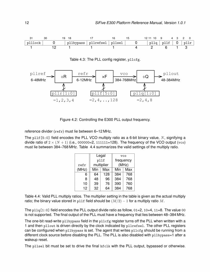
31 30 19 18 17 16 15 12 11 10 9 4 3 2 0
plllock 0 pllbypass pllrefsel pllsel 0 pllq pllf 0 pllr
1 12 1 1 1 4 2 6 1 3
Table 4.3: The PLL config register, pllcfg.
÷R
pllr[1:0]
=1,2,3,4
×F
pllf[5:0]=2,4,..,128
÷Q
pllq[1:0]=2,4,8
pllref refr vco pllout6-48MHz 6-12MHz 384-768MHz 48-384MHz
Figure 4.2: Controlling the E300 PLL output frequency.
reference divider (refr) must lie between 6–12 MHz.
The pllf[5:0] field encodes the PLL VCO multiply ratio as a 6-bit binary value, N , signifying adivide ratio of 2 × (N + 1) (i.e., 000000=2, 111111=128). The frequency of the VCO output (vco)must lie between 384–768 MHz. Table 4.4 summarizes the valid settings of the multiply ratio.
Legal vco
pllf frequencyrefr multiplier (MHz)
(MHz) Min Max Min Max6 64 128 384 7688 48 96 384 768
10 39 76 390 76012 32 64 384 768
Table 4.4: Valid PLL multiply ratios. The multiplier setting in the table is given as the actual multiplyratio; the binary value stored in pllf field should be (M/2) − 1 for a multiply ratio M .
The pllq[1:0] field encodes the PLL output divide ratio as follow, 01=2, 10=4, 11=8. The value 00
is not supported. The final output of the PLL must have a frequency that lies between 48–384 MHz.
The one-bit read-write pllbypass field in the pllcfg register turns off the PLL when written with a1 and then pllout is driven directly by the clock indicated by pllrefsel. The other PLL registerscan be configured when pllbypass is set. The agent that writes pllcfg should be running from adifferent clock source before disabling the PLL. The PLL is also disabled with pllbypass=1 after awakeup reset.
The pllsel bit must be set to drive the final hfclk with the PLL output, bypassed or otherwise.

Copyright c© 2016, SiFive Inc. All rights reserved. 13
When pllsel is clear, the hfroscclk directly drives hfclk. The pllsel bit is clear on wakeupreset.
The pllcfg register is reset to: bypass and power off the PLL pllbypass=1; input driven fromexternal HFXOSC oscillator pllrefsel=1; PLL not driving system clock pllsel=0; and the PLLratios are set to R=2, F=64, and Q=8 (pllr=01, pllf=011111, pllq=11).
The PLL provides a lock signal which is set when the PLL has achieved lock, and which can beread from the most-significant bit of the pllcfg register. The PLL requires up to 100µs to regainlock once enabled, and the lock signal will not necessarily be stable during this initial lock periodso should only be interrogated after this period. The PLL may not achieve lock and the lock signalmight not remain asserted if there is excessive jitter in the source clock.
The PLL requires dedicated 1.8 V power supply pads with a supply filter on the circuit board.The supply filter should be a 100 Ω resistor in series with the board 1.8 V supply decoupled witha 100 nF capacitor across the VDDPLL/VSSPLL supply pins. The VSSPLL pin should not beconnected to board VSS.
PLL Output DividerThe plloutdiv register controls a clock divider that divides the output of the PLL.
0
31 9
plloutdivby1
8
0
7 6
plloutdiv
5 0
Figure 4.3: PLL Output Divider Register plloutdiv
If the plloutdivby1 bit is set, the PLL output clock is passed through undivided. If plloutdivby1is clear, the value N in plloutdiv sets the clock-divide ratio to 2×(N + 1) (between 2–128). Theoutput divider expands the PLL output frequency range to 0.375–384 MHz.
The plloutdivby1 register is reset to divide-by-1 (plloutdivby1=1)..
Internal Low-Frequency Oscillator (LFRCOSC)An untrimmed internal low-frequency RC oscillator can be provided with an operating frequencyof 40-80 kHz. The internal low-frequency oscillator can be used to clock the always-on domain inlieu of an external crystal. A programmable prescalar is provided to allow runtime calibration ofthe low-frequency output to improve timing accuracy.
External 32.768 kHz Low-Frequency Crystal Oscillator (LFXOSC)A 32.768 kHz external crystal oscillator can be attached to provide a precise real-time clock. Theoscillator can be turned off to save power but can require up to 1 s to stabilize.

14 SiFive E300 Platform Reference Manual, Version 1.0.1

Chapter 5
E300 Always-On (AON) Domain
The E300 platform supports an always-on (AON) domain that includes real-time counters, watch-dog timers, backup registers, and reset and power-management circuitry for the rest of the system.Figure 5.1 shows an overview of the AON block.
AON Power Source
The AON domain is continuously powered from an off-chip power source, either a regulated powersupply or a battery.
AON Clocking and Tilelink Slave Port
The AON block has a TileLink slave port to allow an external master to read and write registersinside the AON block. The AON domain is clocked by the low-frequency clock, lfclk. The coredomain’s Tilelink peripheral bus uses the high-frequency tlclk. A HF-LF power-clock-domaincrossing (VCDC) bridges TileLink between the two power and clock domains.
AON Reset Unit
An AON reset is the widest reset on an E300 system, and resets all state except for the JTAGdebug interface.
An AON reset can be triggered by an on-chip power-on reset (POR) circuit when power is firstapplied to the AON domain, an external active-low reset pin (erst n), or expiration of the watchdogtimer (wdogrst).
These sources provide a short initial reset pulse which is extended by the reset stretcher to providea shorter LFROSC reset signal lfroscrst and a longer stretched internal reset, srst.
The lfroscrst signal is used to initialize the ring oscillator in the LFROSC. This oscillator provideslfclk, which is used to clock the AON.
The srst strobe is passed to a reset synchronizer clocked by lfclk to generate aonrst, anasychronous-onset/synchronous-release reset signal used to reset most of the AON block.
15

16 SiFive E300 Platform Reference Manual, Version 1.0.1
Reset Unit
Tile
Link
B4
D32
AON Voltage/Clock Domain
Optional LF crystal oscillatorlfxoscin
lfxoscout
32.768kHz
psdlfclkout
erst_n
External power-on or manual full reset
PORVAON
Reset Stretcher
psdaonrst_n
Observe or generate AON reset pulse
externally
psdaonrsten
aonrst
frst
porrst
srst
erst
dwakeup_n
Optional analog wakeup pinawakeup
LFROSC
lfclk
tlclk
Power Management Unit vddpaden
hfcl
krst
core
rst
Backup Registers≤32 x 32-bit registers
Core Voltage/Clock Domain
msip
mtime
VDC
aonrst
rtcc
mpip
msip
M
Real-Time Clockrtcmpip
tllfclk
wdog
cmpi
p
Watchdogwdogrst
wdogcmpip
psdpmuen
VCDCVAON
VCore
psdlfaltclk
psdcorerst_n
psdhfclkrst_n
psdlfclksel
10
lfroscrst
0
Reset Synchronizer
aonrst
Reset Cause
aonrst
psdaonrstout
Figure 5.1: E300 Always-On Domain.
Power-On Reset CircuitThis optional circuit holds it’s output low until the voltage in the AON block rises above a design-time configurable preset threshold.
External Reset CircuitThe E300 can be reset by pulling down on the external reset pin (erst n), which has a weakpullup. An external power-on reset circuit consisting of a resistor and capacitor can be to providedto generate a sufficiently long pulse to allow supply voltage to rise and then initiate the resetstretcher.
The external reset circuit can add a diode as shown to quickly discharge the capacitor after thesupply is removed to rearm the external power-on reset circuit.
A manual reset button can be connected in parallel over the capacitor.

Copyright c© 2016, SiFive Inc. All rights reserved. 17
Reset CauseThe cause of an AON reset is latched in the Reset Unit and can be read from the pmucause registerin the PMU.
Watchdog Timer (WDT)The watchdog timer can be used to provide a watchdog reset function, or a periodic timer interrupt.The watchdog is described in detail in Chapter 8.
Real-Time Clock (RTC)The real-time clock maintains time for the system and can also be used to generate interrupts fortimed wakeup from sleep-mode or timer interrupts during normal operation. The Real-Time Clockis described in detail in Chapter 9.
Backup RegistersThe backup register provide a configurable number of 32-bit data registers that hold state duringsleep. The FE310-G000 has 16×32-bit backup registers. The backup registers are described indetail in Chapter 10.
Power-Management Unit (PMU)The power-management unit (PMU) sequences the system power supplies and reset signals whentransitioning into and out of sleep mode. The PMU also monitors AON signals for wakeup condi-tions. The PMU is described in detail in Chapter 6.
AON Memory MapTable 5.1 shows the memory map of the AON block.

18 SiFive E300 Platform Reference Manual, Version 1.0.1
Address Description0x1000 0000 wdogcfg
Watchdog Timer Registers
0x1000 0004 Reserved0x1000 0008 wdogcount
0x1000 000C Reserved0x1000 0010 wdogs
0x1000 0014 Reserved0x1000 0018 wdogfeed
0x1000 001C wdogkey
0x1000 0020 wdogcmp
...
0x1000 0040 rtccfg
Real-Time Clock Registers
0x1000 0044 Reserved0x1000 0048 rtclo
0x1000 004C rtchi
0x1000 0050 rtcs
0x1000 0054 Reserved0x1000 0058 Reserved0x1000 005C Reserved0x1000 0060 rtccmp
...
0x1000 0070 lfrosccfg
AON Clock Configuration Registers......
0x1000 0080 backup0
Backup Registers0x1000 0084 backup1
...0x1000 00FC backup31
0x1000 0100 PMU wakeup program memory
Power Management Unit
0x1000 0120 PMU sleep program memory0x1000 0140 pmuie
0x1000 0144 pmucause
0x1000 0148 pmusleep
0x1000 014C pmukey
Table 5.1: SiFive AON Memory Map.
Chapter 6
E300 Power-Management Unit (PMU)
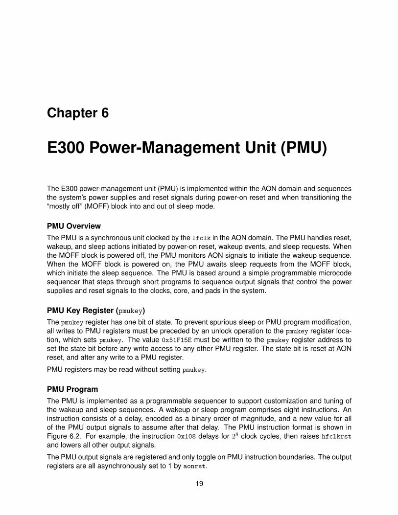
The E300 power-management unit (PMU) is implemented within the AON domain and sequencesthe system’s power supplies and reset signals during power-on reset and when transitioning the“mostly off” (MOFF) block into and out of sleep mode.
PMU OverviewThe PMU is a synchronous unit clocked by the lfclk in the AON domain. The PMU handles reset,wakeup, and sleep actions initiated by power-on reset, wakeup events, and sleep requests. Whenthe MOFF block is powered off, the PMU monitors AON signals to initiate the wakeup sequence.When the MOFF block is powered on, the PMU awaits sleep requests from the MOFF block,which initiate the sleep sequence. The PMU is based around a simple programmable microcodesequencer that steps through short programs to sequence output signals that control the powersupplies and reset signals to the clocks, core, and pads in the system.
PMU Key Register (pmukey)The pmukey register has one bit of state. To prevent spurious sleep or PMU program modification,all writes to PMU registers must be preceded by an unlock operation to the pmukey register loca-tion, which sets pmukey. The value 0x51F15E must be written to the pmukey register address toset the state bit before any write access to any other PMU register. The state bit is reset at AONreset, and after any write to a PMU register.
PMU registers may be read without setting pmukey.
PMU ProgramThe PMU is implemented as a programmable sequencer to support customization and tuning ofthe wakeup and sleep sequences. A wakeup or sleep program comprises eight instructions. Aninstruction consists of a delay, encoded as a binary order of magnitude, and a new value for allof the PMU output signals to assume after that delay. The PMU instruction format is shown inFigure 6.2. For example, the instruction 0x108 delays for 28 clock cycles, then raises hfclkrst
and lowers all other output signals.
The PMU output signals are registered and only toggle on PMU instruction boundaries. The outputregisters are all asynchronously set to 1 by aonrst.
19

20 SiFive E300 Platform Reference Manual, Version 1.0.1
pmuie
dwak
eup
awak
eup
vddp
aden
hfcl
krst
core
rst
rtcc
mpip
pmuprogrampmucauseAON
Tile
Link
pmukey
Signal Condition/Synchronize
resetcause
pmuupc+1
sleep µPC wakeup µPC
delay
Countdown 2N
end?
PMU State Machine
aonrstaonrst
pmusleep
wakeup?
aonrst
sleepwakeup
done
Figure 6.1: E300 Power-Management Unit.
Reserved
31 9
hfclkrst
8
corerst
7
Reserved
6
vddpaden
5
Reserved
4
delay
3 0
Figure 6.2: PMU instruction format.
At power-on reset, the PMU program memories are reset to conservative defaults. Table 6.1 showsthe default wakeup program, and Table 6.2 shows the default sleep program.
Index Value Meaning0 0x1f0 Assert all resets and enable all power supplies1 0x0f8 Idle 28 cycles, then deassert hfclkrst2 0x030 Deassert corerst and padrst
3-7 0x030 Repeats
Table 6.1: Default PMU wakeup program.
Initiate Sleep Sequence Register (pmusleep)
Writing any value to the pmusleep register initiates the sleep sequence stored in the sleep programmemory. The MOFF block will sleep until an event enabled in the pmuie register occurs.

Copyright c© 2016, SiFive Inc. All rights reserved. 21
Index Value Meaning0 0x0f0 Assert corerst1 0x1f0 Assert hfclkrst2 0x1d0 Deassert vddpaden3 0x1c0 Deassert Reserved
4-7 0x1c0 Repeats
Table 6.2: Default PMU sleep program.
Wakeup Signal Conditioning
The PMU can be woken by external signals, dwakeup and awakeup, which are preconditioned bythe signal conditioning block.
Currently, the dwakeup signal has a fixed deglitch circuit that requires the dwakeup signal remainasserted for two AON clock edges before being accepted. The conditioning circuit also resynchro-nizes the dwakeup signal to the AON lfclk.
The awakeup analog intput is not yet supported on E300 systems.
PMU Interrupt Enables (pmuie) and Wakeup Cause (pmucause)
The pmuie register indicates which events can wake the MOFF block from sleep. The awakeup bitindicates that the awakeup pin can rouse MOFF. The dwakeup bit indicates that a logic 0 on thedwakeup n pin can rouse MOFF. The rtc bit indicates that the RTC comparator can rouse MOFF.
Reserved
31 4
awakeup
3
dwakeup
2
rtc
1
Reserved
0
Figure 6.3: Format of pmuie register.
Following a wakeup, the pmucause register indicates which event caused the wakeup. The valuein the wakeupcause field corresponds to the bit position of the event in pmuie, e.g., a value of 2indicates dwakeup. The value 0 indicates a wakeup from reset.
Reserved
31 10
resetcause
9 8
Reserved
7 2
wakeupcause
1 0
Figure 6.4: Format of pmucause register.
In the event of a wakeup from reset, the resetcause field indicates which reset source triggeredthe wakeup. Table 6.3 lists the values the resetcause field may take. The value in resetcause
persists until the next reset.
22 SiFive E300 Platform Reference Manual, Version 1.0.1
Index Meaning0 Power-on reset1 External reset2 Watchdog timer reset
Table 6.3: Reset cause values.
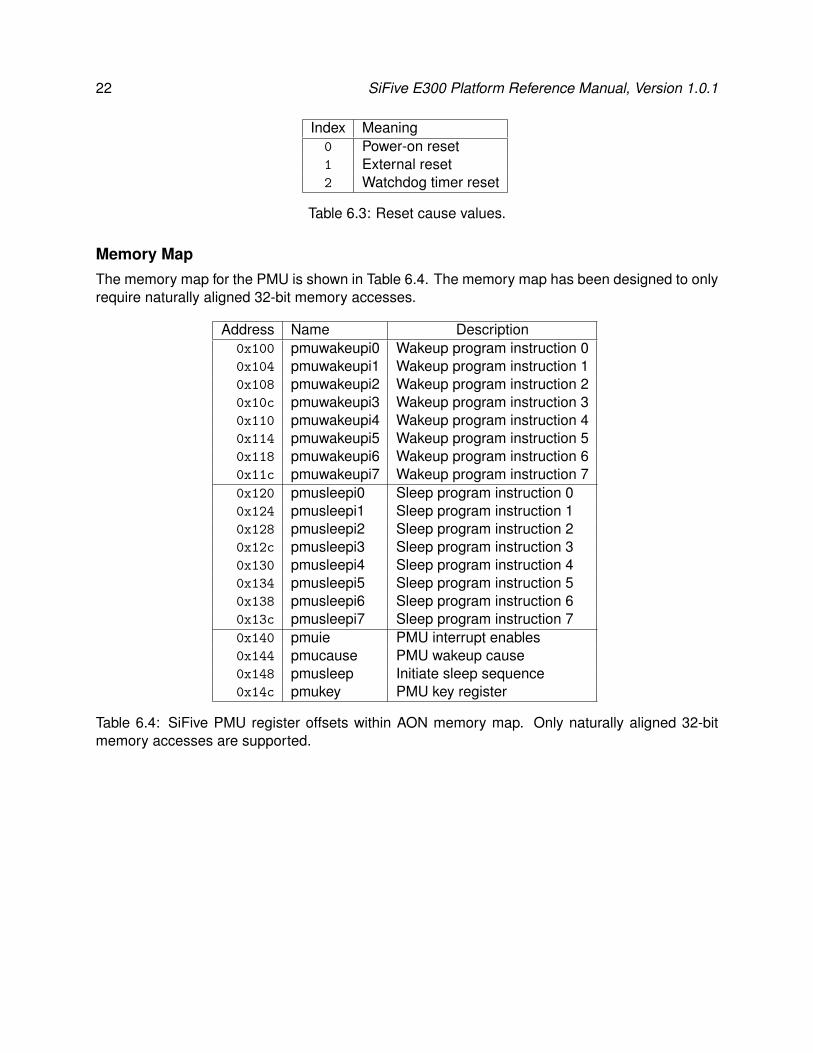
Memory MapThe memory map for the PMU is shown in Table 6.4. The memory map has been designed to onlyrequire naturally aligned 32-bit memory accesses.
Address Name Description0x100 pmuwakeupi0 Wakeup program instruction 00x104 pmuwakeupi1 Wakeup program instruction 10x108 pmuwakeupi2 Wakeup program instruction 20x10c pmuwakeupi3 Wakeup program instruction 30x110 pmuwakeupi4 Wakeup program instruction 40x114 pmuwakeupi5 Wakeup program instruction 50x118 pmuwakeupi6 Wakeup program instruction 60x11c pmuwakeupi7 Wakeup program instruction 70x120 pmusleepi0 Sleep program instruction 00x124 pmusleepi1 Sleep program instruction 10x128 pmusleepi2 Sleep program instruction 20x12c pmusleepi3 Sleep program instruction 30x130 pmusleepi4 Sleep program instruction 40x134 pmusleepi5 Sleep program instruction 50x138 pmusleepi6 Sleep program instruction 60x13c pmusleepi7 Sleep program instruction 70x140 pmuie PMU interrupt enables0x144 pmucause PMU wakeup cause0x148 pmusleep Initiate sleep sequence0x14c pmukey PMU key register
Table 6.4: SiFive PMU register offsets within AON memory map. Only naturally aligned 32-bitmemory accesses are supported.
Chapter 7
E300 Power, Reset, Clock, Interrupt(PRCI) Control and Status Registers
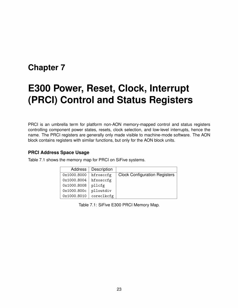
PRCI is an umbrella term for platform non-AON memory-mapped control and status registerscontrolling component power states, resets, clock selection, and low-level interrupts, hence thename. The PRCI registers are generally only made visible to machine-mode software. The AONblock contains registers with similar functions, but only for the AON block units.
PRCI Address Space UsageTable 7.1 shows the memory map for PRCI on SiFive systems.
Address Description0x1000 8000 hfrosccfg Clock Configuration Registers0x1000 8004 hfxosccfg
0x1000 8008 pllcfg
0x1000 800c plloutdiv
0x1000 8010 coreclkcfg
Table 7.1: SiFive E300 PRCI Memory Map.
23

24 SiFive E300 Platform Reference Manual, Version 1.0.1

Chapter 8
E300 Watchdog Timer (WDT)
The watchdog timer (WDT) is used to cause a full power-on reset if either hardware or softwareerrors cause the system to malfunction. The WDT can also be used as a programmable periodicinterrupt source if the watchdog functionality is not required. The WDT is implemented as anupcounter in the Always-On domain that must be reset at regular intervals before the count reachesa preset threshold, else it will trigger a full power-on reset. To prevent errant code from resettingthe counter, the WDT registers can only be updated by presenting a WDT key sequence.
wdogcmp
wdogcfg
wdogcmpip
wdogclk
aonrst
wdogcount
wdogs wdogscale
>=?
Wdo
g Ti
leLi
nk
wdogfeed
reset
wdogrst
aonrst
en
wdogclk
wdogkey
corerstSynch
wdogzerocmp
wdogrsten
wdogenalways
wdogencoreawake
Figure 8.1: E300 Watchdog Timer.
Watchdog Count Register (wdogcount)The WDT is based around a 31-bit counter held in wdogcount[30:0]. The counter can be read orwritten over the TileLink bus. Bit 31 of wdogcount returns a zero when read.
25
26 SiFive E300 Platform Reference Manual, Version 1.0.1
The counter is incremented at a maximum rate determined by the watchdog clock selection. Eachcycle, the counter can be conditionally incremented depending on the existence of certain condi-tions, including always incrementing or incrementing only when the processor is not asleep.
The counter can also be reset to zero depending on certain conditions, such as a successful writeto wdogfeed or the counter matching the compare value.
Watchdog Clock Selection
The WDT unit clock, wdogclk, is either driven from LFXOSC or LFRCOSC and runs at approxi-mately 32 kHz.
Watchdog Configuration Register wdogcfg
Reserved
31 29
wdogcmpip
28
Reserved
27 14
wdogencoreawake
13
wdogenalways
12
Reserved
11 10
wdogzerocmp
9
wdogrsten
8
Reserved
7 4
wdogscale
3 0
Figure 8.2: Watchdog configuration register wdogcfg
The wdogen* bits control the conditions under which the watchdog counter wdogcount is incre-mented. The wdogenalways bit if set means the watchdog counter always increments. Thewdogencoreawake bit if set means the watchdog counter increments if the processor core is notasleep. The WDT uses the corerst signal from the wakeup sequencer to know when the core issleeping. The counter increments by one each cycle only if any of the enabled conditions are true.The wdogen* bits are reset on AON reset.
The 4-bit wdogscale field scales the watchdog counter value before feeding it to the comparator.The value in wdogscale is the bit position within the wdogcount register of the start of a 16-bitwdogs field. A value of 0 in wdogscale indicates no scaling, and wdogs would then be equal tothe low 16 bits of wdogcount. The maximum value of 15 in wdogscale corresponds to dividing theclock rate by 215, so for an input clock of 32.768 kHz, the LSB of wdogs will increment once persecond.
The value of wdogs is memory-mapped and can be read as a single 16-bit value over the AONTileLink bus.
The wdogzerocmp bit, if set, causes the watchdog counter wdogcount to be automatically reset tozero one cycle after the wdogs counter value matches or exceeds the compare value in wdogcmp.This feature can be used to implement periodic counter interrupts, where the period is independentof interrupt service time.
The wdogrsten bit controls whether the comparator output can set the wdogrst bit and hencecause a full reset.
The wdogcmpip interrupt pending bit can be read or written.
Copyright c© 2016, SiFive Inc. All rights reserved. 27
Reserved
31 16
wdogcmp[15:0]
15 0
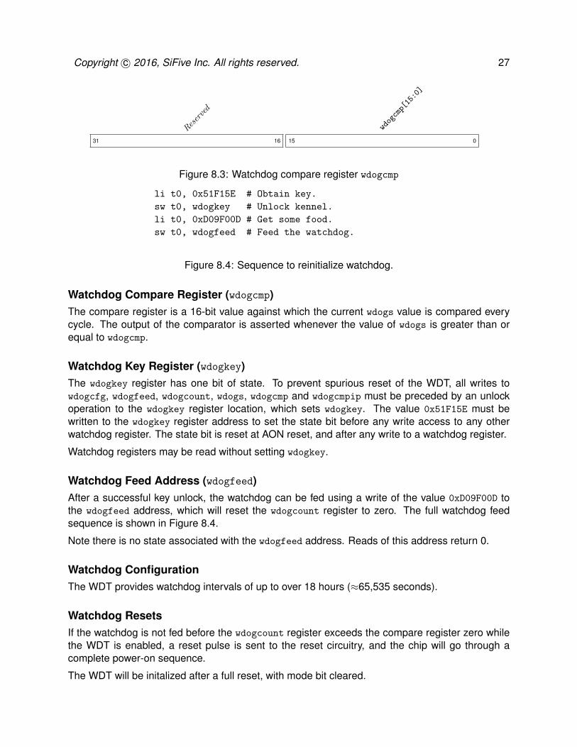
Figure 8.3: Watchdog compare register wdogcmp
li t0, 0x51F15E # Obtain key.
sw t0, wdogkey # Unlock kennel.
li t0, 0xD09F00D # Get some food.
sw t0, wdogfeed # Feed the watchdog.
Figure 8.4: Sequence to reinitialize watchdog.
Watchdog Compare Register (wdogcmp)The compare register is a 16-bit value against which the current wdogs value is compared everycycle. The output of the comparator is asserted whenever the value of wdogs is greater than orequal to wdogcmp.
Watchdog Key Register (wdogkey)The wdogkey register has one bit of state. To prevent spurious reset of the WDT, all writes towdogcfg, wdogfeed, wdogcount, wdogs, wdogcmp and wdogcmpip must be preceded by an unlockoperation to the wdogkey register location, which sets wdogkey. The value 0x51F15E must bewritten to the wdogkey register address to set the state bit before any write access to any otherwatchdog register. The state bit is reset at AON reset, and after any write to a watchdog register.
Watchdog registers may be read without setting wdogkey.
Watchdog Feed Address (wdogfeed)After a successful key unlock, the watchdog can be fed using a write of the value 0xD09F00D tothe wdogfeed address, which will reset the wdogcount register to zero. The full watchdog feedsequence is shown in Figure 8.4.
Note there is no state associated with the wdogfeed address. Reads of this address return 0.
Watchdog ConfigurationThe WDT provides watchdog intervals of up to over 18 hours (≈65,535 seconds).
Watchdog ResetsIf the watchdog is not fed before the wdogcount register exceeds the compare register zero whilethe WDT is enabled, a reset pulse is sent to the reset circuitry, and the chip will go through acomplete power-on sequence.
The WDT will be initalized after a full reset, with mode bit cleared.

28 SiFive E300 Platform Reference Manual, Version 1.0.1
Watchdog Interrupts (wdogcmpip)The WDT can be configured to provide periodic counter interrupts by disabling watchdog re-sets (wdogrsten=0) and enabling auto-zeroing of the count register when the comparator fires(wdogzerocmp=1).
The sticky single-bit wdogcmpip register captures the comparator output and holds it to provide aninterrupt pending signal. The wdogcmpip register resides in bit 28 of the wdogcfg register, and canbe read and written over TileLink to clear down the interrupt.

Chapter 9
E300 Real-Time Clock (RTC)
The E300 real-time clock (RT) is located in the always-on domain, and is clocked by a se-lectable low-frequency clock source. For best accuracy, the RTC should be driven by an external32.768 kHz watch crystal oscillator (LFXOSC), but to reduce cost, can be driven by a factory-trimmed on-chip oscillator.
rtccmp
rtchi
rtccfg
AON
Tile
Link
rtccmpip
lfclk
aonrst
rtclo
rtcs
rtcen
rtcscale
>=?
Figure 9.1: E300 Real-Time Clock.
RTC Count Registers rtchi/rtclo
The real-time counter is based around the rtchi/rtclo register pair, which increment at the low-frequency clock rate when the RTC is enabled. The rtclo register holds the low 32 bits of the RTC,while rtchi holds the upper 16 bits of the RTC value. The total ≥48-bit counter width ensuresthere will no counter rollover for over 270 years assuming a 32.768 kHz low-frequency real-timeclock source. The counter registers can be read or written over the TileLink bus.
RTC Configuration Register rtccfg
The rtcenalways bit controls whether the RTC is enabled, and is reset on AON reset.
29

30 SiFive E300 Platform Reference Manual, Version 1.0.1
Reserved
31 16
rtchi
15 0
rtclo
31 0
Figure 9.2: RTC counter register pair rtchi/rtclo
Reserved
31 29
rtcmpip
28
Reserved
27 13
rtcenalways
12
Reserved
11 4
rtcscale
3 0
Figure 9.3: RTC configuration register rtccfg
The 4-bit rtcscale field scales the real-time counter value before feeding to the real-time interruptcomparator. The value in rtcscale is the bit position within the rtclo/rtchi register pair of thestart of a 32-bit field rtcs. A value of 0 in rtcscale indicates no scaling, and rtcs would then beequal to rtclo. The maximum value of 15 in rtcscale corresponds to dividing the clock rate by215, so for an input clock of 32.768 kHz, the LSB of rtcs will increment once per second. The valueof rtcs is memory-mapped and can be read as a single 32-bit register over the AON TileLink bus.
The rtccmpip interrupt pending bit is read-only.
RTC Compare Register rtccmpThe rtccmp register holds a 32-bit value that is compared against rtcs, the scaled real-time clock.If rtcs is greater than or equal to rtccmp, the rtccmpip interrupt pending bit is set. The rtccmpip
bit can be cleared down by writing a value to rtccmp that is greater than rtcs.
rtccmp
31 0
Figure 9.4: RTC counter compare register rtccmp
Chapter 10
E300 Backup Registers
The backup registers live in the Always-On domain, and provide a place to store critical data duringsleep. Each register is 32-bits wide, and the number of backup registers is a configurable option.
31

32 SiFive E300 Platform Reference Manual, Version 1.0.1

Chapter 11
General Purpose Input/OutputController (GPIO)
This chapter describes the operation of the General Purpose Input/Output Controller (GPIO) onSiFive systems. The SiFive GPIO controller is a peripheral device mapped in the internal memorymap, discoverable in the Configuration String. It is responsible for low-level configuration of theactual GPIO pads on the device (direction, pull up-enable, and drive value), as well as selectingbetween various sources of the controls for these signals. The GPIO controller allows seperateconfiguration of each of N GPIO bits. Figure 11.1 shows the control structure for each pin.
Atomic operations such as toggles are natively possible with the RISC-V ’A’ extension.
Memory MapThe memory map for the SiFive GPIO control registers is shown in Table 11.1. The GPIO memorymap has been designed to only require naturally aligned 32-bit memory accesses.
Input / Output ValuesThe same port register can be configured on a bitwise fashion to represent either inputs or out-puts, as set by the direction register. Writing to the port register will update the bits regardlessof the tristate value. Reading the port register will return the written value. Reading the value
register will return the actual value of the pin.
In other words, on a read:
value = (input & direction) | (output & ~direction)
InterruptsA single interrupt bit can be generated for each GPIO bit. The interrupt can be driven by rising orfalling edges, or by level values, and each can be enabled individually.
Inputs are synchronized before being sampled by the interrupt logic, so the input pulse width mustbe long enough to be detected by the synchronization logic.
To enable an interrupt, set the corresponding bit in the rise ie and/or fall ie to 1. If the correp-sonding bit in rise ip or fall ip is set, an interrupt pin will be raised.
33

34 SiFive E300 Platform Reference Manual, Version 1.0.1
D Q
PUE
D Q
OVAL
Q D
VALUE
D Q
IOF_EN
D Q
IOF_SEL
D Q
OE
IOF1_OVAL
0
1
IOF_OUTIOF_OE
0
1 OEN
I
PE
Q D
SyncQ D
C
Not Shown:Low Power Clamping
Wake-on-Interrupt LogicIOF Signal Derivation
D Q
HIGH_IP
D Q
LOW_IP
D Q
RISE_IP
D Q
FALL_IP
IOF_IVAL
D Q
HIGH_IE
D Q
LOW_IE
D Q
RISE_IE
D Q
FALL_IE
INTERRUPT
DS
IOF1_OE
…
IOF0_OVALIOF0_OE
D Q
DS
PUED Q
IE
IVAL
OVAL
DS
OE…
IE IE
…
Q D
OUT_XOR
Figure 11.1: Structure of a single GPIO Pin with Control Registers. This structure is repeated foreach pin.
Copyright c© 2016, SiFive Inc. All rights reserved. 35
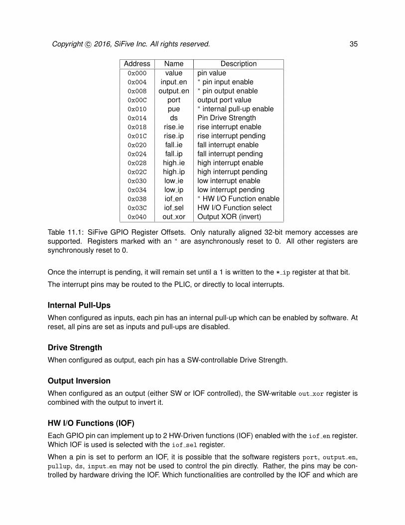
Address Name Description0x000 value pin value0x004 input en ∗ pin input enable0x008 output en ∗ pin output enable0x00C port output port value0x010 pue ∗ internal pull-up enable0x014 ds Pin Drive Strength0x018 rise ie rise interrupt enable0x01C rise ip rise interrupt pending0x020 fall ie fall interrupt enable0x024 fall ip fall interrupt pending0x028 high ie high interrupt enable0x02C high ip high interrupt pending0x030 low ie low interrupt enable0x034 low ip low interrupt pending0x038 iof en ∗ HW I/O Function enable0x03C iof sel HW I/O Function select0x040 out xor Output XOR (invert)
Table 11.1: SiFive GPIO Register Offsets. Only naturally aligned 32-bit memory accesses aresupported. Registers marked with an ∗ are asynchronously reset to 0. All other registers aresynchronously reset to 0.
Once the interrupt is pending, it will remain set until a 1 is written to the * ip register at that bit.
The interrupt pins may be routed to the PLIC, or directly to local interrupts.
Internal Pull-UpsWhen configured as inputs, each pin has an internal pull-up which can be enabled by software. Atreset, all pins are set as inputs and pull-ups are disabled.
Drive StrengthWhen configured as output, each pin has a SW-controllable Drive Strength.
Output InversionWhen configured as an output (either SW or IOF controlled), the SW-writable out xor register iscombined with the output to invert it.
HW I/O Functions (IOF)Each GPIO pin can implement up to 2 HW-Driven functions (IOF) enabled with the iof en register.Which IOF is used is selected with the iof sel register.
When a pin is set to perform an IOF, it is possible that the software registers port, output en,pullup, ds, input en may not be used to control the pin directly. Rather, the pins may be con-trolled by hardware driving the IOF. Which functionalities are controlled by the IOF and which are

36 SiFive E300 Platform Reference Manual, Version 1.0.1
controlled by the software registers are fixed in the hardware on a per-IOF basis. Those that arenot controlled by the hardware continue to be controlled by the software registers.
If there is no IOFx for a pin configured with IOFx, the pin reverts to full software control.
Behavior During Sleep Mode
Chapter 12
Universal AsynchronousReceiver/Transmitter (UART)
This chapter describes the operation of the SiFive Universal Asynchronous Receiver/Transmitter(UART).
UART Overview
The UART peripheral supports the following features:
• 8-N-1 and 8-N-2 formats: 8 data bits, no parity bit, 1 start bit, 1 or 2 stop bits• 8-entry transmit and receive FIFO buffers with programmable watermark interrupts• 16× Rx oversampling with 2/3 majority voting per bit
The UART peripheral does not support hardware flow control or other modem control signals, orsynchronous serial data tranfesrs.
Memory Map
The memory map for the UART control registers is shown in Table 12.1. The UART memory maphas been designed to only require naturally aligned 32-bit memory accesses.
Address Name Description0x000 txdata Transmit data register0x004 rxdata Receive data register0x008 txctrl Transmit control register0x00C rxctrl Receive control register0x010 ie UART interrupt enable0x014 ip UART Interrupt pending0x018 div Baud rate divisor
Table 12.1: Register offsets within UART memory map.
37
38 SiFive E300 Platform Reference Manual, Version 1.0.1
Transmit Data Register (txdata)
Writing to the txdata register enqueues the character contained in the data field to the transmitFIFO if the FIFO is able to accept new entries. Reading from txdata returns the current value ofthe full flag and zero in the data field. The full flag indicates whether the transmit FIFO is ableto accept new entries; when set, writes to data are ignored. A RISC-V amoswap instruction canbe used to both read the full status and attempt to enqueue data, with a non-zero return valueindicating the character was not accepted.
full
31
0
30 8
data
7 0
Figure 12.1: Format of txdata register.
Receive Data Register (rxdata)
Reading the rxdata register dequeues a character from the receive FIFO, and returns the valuein the data field. The empty flag indicates if the receive FIFO was empty; when set, the data fielddoes not contain a valid character. Writes to rxdata are ignored.
empty
31
0
30 8
data
7 0
Figure 12.2: Format of rxdata register.
Transmit Control Register (txctrl)
The read-write txctrl register controls the operation of the transmit channel. The txen bit controlswhether the Tx channel is active. When cleared, transmission of Tx FIFO contents is suppressed,and the txd pin is driven high.
The nstop field specifies the number of stop bits: 0 for one stop bit and 1 for two stop bits.
The txcnt field specifies the threshold at which the Tx FIFO watermark interrupt triggers.
The txctrl register is reset to 0.
Reserved
31 19
txcnt
18 16
Reserved
15 2
nstop
1
txen
0
Figure 12.3: Format of txctrl register.
Copyright c© 2016, SiFive Inc. All rights reserved. 39
Receive Control Register (rxctrl)
The read-write rxctrl register controls the operation of the receive channel. The rxen bit controlswhether the Rx channel is active. When cleared, the state of the rxd pin is ignored, and nocharacters will be enqueued into the Rx FIFO.
The rxcnt field specifies the threshold at which the Rx FIFO watermark interrupt triggers.
The rxctrl register is reset to 0.
Reserved
31 19
rxcnt
18 16
Reserved
15 1
rxen
0
Figure 12.4: Format of rxctrl register.
Interrupt Registers (ip and ie)
The ip register is a read-only register indicating the pending interrupt conditions, and the read-write ie register controls which UART interrupts are enabled. ie is reset to 0.
The txwm condition becomes raised when the number of entries in the transmit FIFO is strictly lessthan the count specified by the txcnt field of the txctrl register. The pending bit is cleared whensufficient entries have been enqueued to exceed the watermark.
The rxwm condition becomes raised when the number of entries in the receive FIFO is strictlygreater than the count specified by the rxcnt field of the rxctrl register. The pending bit iscleared when sufficient entries have been dequeued to fall below the watermark.
0
31 2
rxwm
1
txwm
0
Figure 12.5: Format of ie and ip registers.
Baud Rate Divisor Register (div)
The read-write div register specifies the divisor used by baud rate generation for both Tx and Rxchannels. The relationship between the input clock and baud rate is given by the following formula:
fbaud =fin
div + 1
0
31 16
div
15 0
Figure 12.6: Format of div register.
40 SiFive E300 Platform Reference Manual, Version 1.0.1
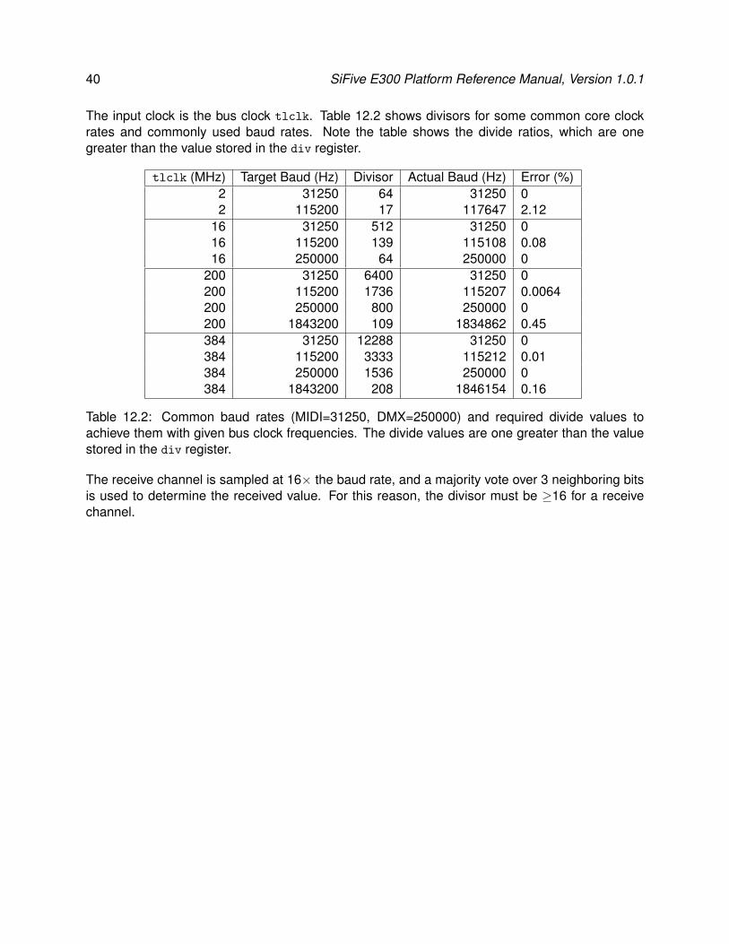
The input clock is the bus clock tlclk. Table 12.2 shows divisors for some common core clockrates and commonly used baud rates. Note the table shows the divide ratios, which are onegreater than the value stored in the div register.
tlclk (MHz) Target Baud (Hz) Divisor Actual Baud (Hz) Error (%)2 31250 64 31250 02 115200 17 117647 2.12
16 31250 512 31250 016 115200 139 115108 0.0816 250000 64 250000 0
200 31250 6400 31250 0200 115200 1736 115207 0.0064200 250000 800 250000 0200 1843200 109 1834862 0.45384 31250 12288 31250 0384 115200 3333 115212 0.01384 250000 1536 250000 0384 1843200 208 1846154 0.16
Table 12.2: Common baud rates (MIDI=31250, DMX=250000) and required divide values toachieve them with given bus clock frequencies. The divide values are one greater than the valuestored in the div register.
The receive channel is sampled at 16× the baud rate, and a majority vote over 3 neighboring bitsis used to determine the received value. For this reason, the divisor must be ≥16 for a receivechannel.
Chapter 13
Serial Peripheral Interface (SPI)
This chapter describes the operation of the SiFive Serial Peripheral Interface (SPI) controller.
SPI OverviewThe SPI controller supports master-only operation over the single-lane, dual-lane, and quad-laneprotocols. The baseline controller provides a FIFO-based interface for performing programmedI/O. Software initiates a transfer by enqueuing a frame in the transmit FIFO; when the transfercompletes, the slave response is placed in the receive FIFO.
In addition, the dedicated SPI0 controller implements a SPI flash read sequencer, which exposesthe external SPI flash contents as a read/execute-only memory-mapped device. The SPI0 con-troller is reset to a state which allows memory-mapped reads, under the assumption that the inputclock rate is less than 100 MHz and the external SPI flash device supports the common Win-bond/Numonyx serial read (0x03) command. Sequential accesses are automatically combinedinto one long read command for higher performance.
The fctrl register controls switching between the memory-mapped and programmed-I/O modes.While in programmed-I/O mode, memory-mapped reads do not access the external SPI flashdevice and instead return 0 immediately. Hardware interlocks ensure that the current transfercompletes before mode transitions and control register updates take effect.
Memory MapThe memory map for the SPI control registers is shown in Table 13.1. The SPI memory map hasbeen designed to only require naturally aligned 32-bit memory accesses.
Serial Clock Divisor Register (sckdiv)The sckdiv register specifies the divisor used for generating the serial clock (SCK). The relation-ship between the input clock and SCK is given by the following formula:
fsck =fin
2(div + 1)
The input clock is the bus clock tlclk. The reset value of the div field is 0x003.
41
42 SiFive E300 Platform Reference Manual, Version 1.0.1
Address Name Description0x000 sckdiv Serial clock divisor0x004 sckmode Serial clock mode0x010 csid Chip select ID0x014 csdef Chip select default0x018 csmode Chip select mode0x028 delay0 Delay control 00x02C delay1 Delay control 10x040 fmt Frame format0x048 txdata Tx FIFO data0x04C rxdata Rx FIFO data0x050 txmark Tx FIFO watermark0x054 rxmark Rx FIFO watermark0x060 fctrl* SPI flash interface control0x064 ffmt* SPI flash instruction format0x070 ie SPI interrupt enable0x074 ip SPI interrupt pending
Table 13.1: Register offsets within the SPI memory map. Registers marked * are present only oncontrollers with the direct-map flash interface, i.e., SPI0.
Reserved
31 12
div
11 0
Figure 13.1: Format of sckdiv register.
Serial Clock Mode Register (sckmode)
The sckmode register defines the serial clock polarity and phase. Tables 13.2 and 13.3 describethe behavior of the pol and pha fields, respectively. The reset value of sckmode is 0.
Reserved
31 2
pol
1
pha
0
Figure 13.2: Format of sckmode register.
Value Description0 Inactive state of SCK is logical 01 Inactive state of SCK is logical 1
Table 13.2: Serial clock polarity.
Copyright c© 2016, SiFive Inc. All rights reserved. 43
Value Description0 Data is sampled on the leading edge of SCK and shifted on the trailing edge of SCK1 Data is shifted on the leading edge of SCK and sampled on the trailing edge of SCK
Table 13.3: Serial clock phase.
Chip Select ID Register (csid)
The csid register encodes the index of the CS pin to be toggled by hardware chip select control.The reset value is 0.
csid
31 0
Figure 13.3: Format of csid register.
Chip Select Default Register (csdef)
The csdef register specifies the inactive state (polarity) of the CS pins. The reset value is 0xFFFF.
csdef
31 0
Figure 13.4: Format of csdef register.
Chip Select Mode Register (csmode)
The csmode register defines the hardware chip select behavior as described in Table 13.4. Thereset value is 0 (AUTO). In HOLD mode, the CS pin is de-asserted only when one of the followingconditions occur:
• A different value is written to csmode or csid.• A write to csdef changes the state of the selected pin.• Direct-mapped flash mode is enabled.
Reserved
31 2
mode
1 0
Figure 13.5: Format of csmode register.

44 SiFive E300 Platform Reference Manual, Version 1.0.1
Value Name Description0 AUTO Assert/de-assert CS at the beginning/end of each frame2 HOLD Keep CS continuously asserted after the initial frame3 OFF Disable hardware control of the CS pin
Table 13.4: Chip select modes.
Delay Control Registers (delay0 and delay1)
The delay0 and delay1 registers allow for the insertion of arbitrary delays specified in units of oneSCK period.
The cssck field specifies the delay between the assertion of CS and the first leading edge of SCK.When sckmode.pha = 0, an additional half-period delay is implicit. The reset value is 0x01.
The sckcs field specifies the delay between the last trailing edge of SCK and the de-assertion ofCS. When sckmode.pha = 1, an additional half-period delay is implicit. The reset value is 0x01.
The intercs field specifies the minimum CS inactive time between de-assertion and assertion.The reset value is 0x01.
The interxfr field specifies the delay between two consecutive frames without de-asserting CS.This is applicable only when sckmode is HOLD or OFF. The reset value is 0x00.
Reserved
31 24
sckcs
23 16
Reserved
15 8
cssck
7 0
Figure 13.6: Format of delay0 register.
Reserved
31 24
interxfr
23 16
Reserved
15 8
intercs
7 0
Figure 13.7: Format of delay1 register.
Frame Format Register (fmt)
The fmt register defines the frame format for transfers initiated through the programmed-I/O (FIFO)interface. Tables 13.5, 13.6, and 13.7 describe the proto, endian, and dir fields, respectively. Thelen field defines the number of bits per frame, where the allowed range is 0 to 8 inclusive.
The reset value is 0x80000, corresponding to proto = single, dir = Rx, endian = MSB, andlen = 8.

Copyright c© 2016, SiFive Inc. All rights reserved. 45
Reserved
31 20
len
19 16
Reserved
15 4
dir
3
endian
2
proto
1 0
Figure 13.8: Format of fmt register.
Value Description Data Pins0 Single DQ0 (MOSI), DQ1 (MISO)1 Dual DQ0, DQ12 Quad DQ0, DQ1, DQ2, DQ3
Table 13.5: SPI protocol. Unused DQ pins are tri-stated.
Value Description0 Transmit most-significant bit (MSB) first1 Transmit least-significant bit (LSB) first
Table 13.6: SPI endianness.
Value Description0 Rx: For dual and quad protocols, the DQ pins are tri-stated. For the single
protocol, the DQ0 pin is driven with the transmit data as normal.1 Tx: The receive FIFO is not populated.
Table 13.7: SPI I/O direction.
Transmit Data Register (txdata)Writing to the txdata register loads the transmit FIFO with the value contained in the data field.For fmt.len < 8, values should be left-aligned when fmt.endian = MSB and right-aligned whenfmt.endian = LSB.
The full flag indicates whether the transmit FIFO is ready to accept new entries; when set, writesto txdata are ignored. The data field returns 0x00 when read.
full
31
Reserved
30 8
data
7 0
Figure 13.9: Format of txdata register.
Receive Data Register (rxdata)Reading the rxdata register dequeues a frame from the receive FIFO. For fmt.len < 8, valuesare left-aligned when fmt.endian = MSB and right-aligned when fmt.endian = LSB.
46 SiFive E300 Platform Reference Manual, Version 1.0.1
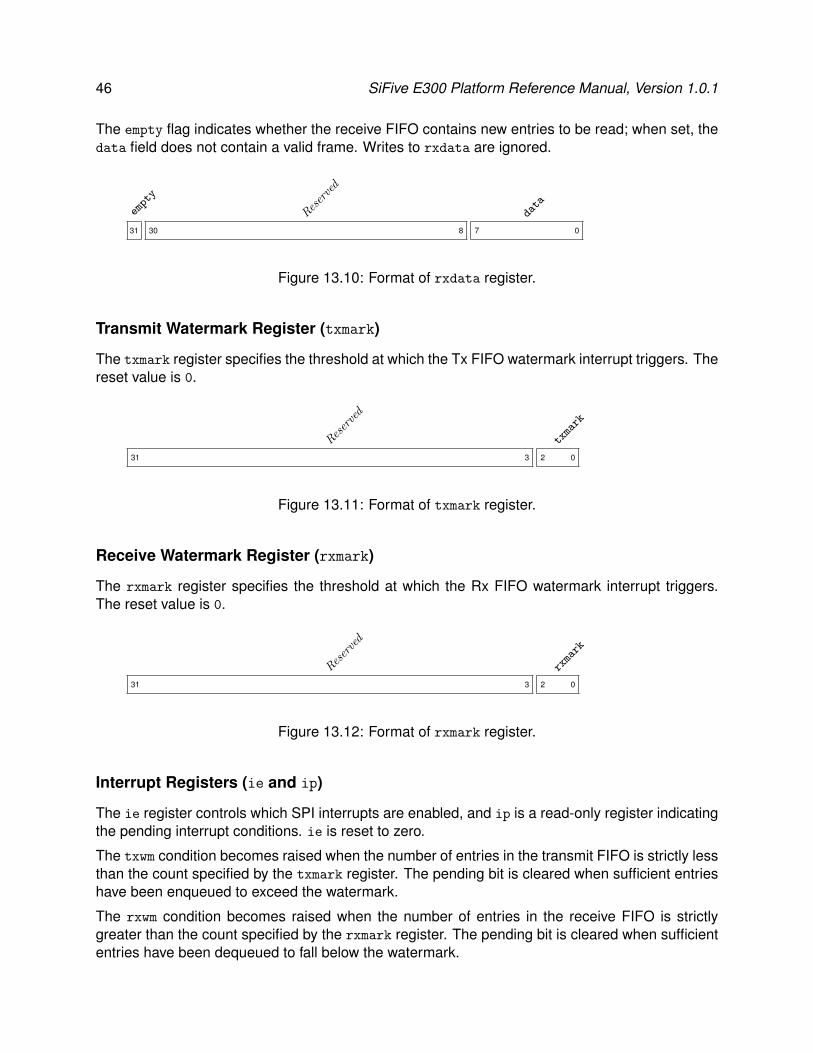
The empty flag indicates whether the receive FIFO contains new entries to be read; when set, thedata field does not contain a valid frame. Writes to rxdata are ignored.
empty
31
Reserved
30 8
data
7 0
Figure 13.10: Format of rxdata register.
Transmit Watermark Register (txmark)
The txmark register specifies the threshold at which the Tx FIFO watermark interrupt triggers. Thereset value is 0.
Reserved
31 3
txmark
2 0
Figure 13.11: Format of txmark register.
Receive Watermark Register (rxmark)
The rxmark register specifies the threshold at which the Rx FIFO watermark interrupt triggers.The reset value is 0.
Reserved
31 3
rxmark
2 0
Figure 13.12: Format of rxmark register.
Interrupt Registers (ie and ip)
The ie register controls which SPI interrupts are enabled, and ip is a read-only register indicatingthe pending interrupt conditions. ie is reset to zero.
The txwm condition becomes raised when the number of entries in the transmit FIFO is strictly lessthan the count specified by the txmark register. The pending bit is cleared when sufficient entrieshave been enqueued to exceed the watermark.
The rxwm condition becomes raised when the number of entries in the receive FIFO is strictlygreater than the count specified by the rxmark register. The pending bit is cleared when sufficiententries have been dequeued to fall below the watermark.

Copyright c© 2016, SiFive Inc. All rights reserved. 47
Reserved
31 2
rxwm
1
txwm
0
Figure 13.13: Format of ie and ie registers.
SPI Flash Interface Control Register (fctrl)When the en bit of the fctrl register is set, the controller enters SPI flash mode. Accesses to thedirect-mapped memory region causes the controller to automatically sequence SPI flash reads inhardware. The reset value is 0x1.
Reserved
31 1
en
0
Figure 13.14: Format of fctrl register.
SPI Flash Instruction Format Register (ffmt)The ffmt register defines the format of the SPI flash read instruction issued by the controller whenthe direct-mapped memory region is accessed while in SPI flash mode.
An instruction consists of a command byte followed by a variable number of address bytes, dummycycles (padding), and data bytes. Table 13.8 describes the function and reset value of each field.
padcode
31 24
cmdcode
23 16
Reserved
15
dataproto
13 12
addrproto
11 10
cmdproto
9 8
padcnt
7 4
addrlen
3 1
cmden
0
Figure 13.15: Format of ffmt register.
Field Description Reset Valuecmd en Enable sending of command 0x1
cmd code Value of command byte 0x03
cmd proto Protocol for transmitting command 0x0
addr len Number of address bytes (0 to 4) 0x3
addr proto Protocol for transmitting address and padding 0x0
pad cnt Number of dummy cycles 0x0
pad code First 8 bits to transmit during dummy cycles 0x00
data proto Protocol for receiving data bytes 0x0
Table 13.8: Instruction format fields. The protocol values follow the same definition as Table 13.5.

48 SiFive E300 Platform Reference Manual, Version 1.0.1

Chapter 14
One-Time Programmable Memory(OTP) Peripheral
This chapter describes the operation of the One-Time Programmable Memory (OTP) Controlleron SiFive systems.
Device configuration and power-supply control is principally under software control. The controlleris reset to a state that allows memory-mapped reads, under the assumption that the controller’sclock rate is between 1 MHz and 37 MHz. vrren is asserted during synchronous reset; it is safe toread from OTP immediately after reset if reset is asserted for at least ???µs while the controller’sclock is running.
Programmed-I/O reads and writes are sequenced entirely by software.
Memory MapThe memory map for the OTP control registers is shown in Table 14.1. The control-register mem-ory map has been designed to only require naturally aligned 32-bit memory accesses. The OTPcontroller also contains a read sequencer, which exposes the OTP’s contents as a read/execute-only memory-mapped device.
Programmed-I/O lock register (otp lock)The otp lock register supports synchronization between the read sequencer and theprogrammed-I/O interface. When the lock is clear, memory-mapped reads may proceed. Whenthe lock is set, memory-mapped reads do not access the OTP device, and instead return 0 imme-diately.
The otp lock should be acquired before writing to any other control register. Software can attemptto acquire the lock by storing 1 to otp lock. If a memory-mapped read is in progress, the lock willnot be acquired, and will retain the value 0. Software can check if the lock was successfullyacquired by loading otp lock and checking that it has the value 1.
After a programmed-I/O sequence, software should restore the previous value of any control reg-isters that were modified, then store 0 to otp lock.
Figure 14.1 shows the synchronization code sequence.
49

50 SiFive E300 Platform Reference Manual, Version 1.0.1
Address Name Description0x00 otp lock Programmed-I/O lock register0x04 otp ck OTP device clock signal0x08 otp oe OTP device output-enable signal0x0c otp sel OTP device chip-select signal0x10 otp we OTP device write-enable signal0x14 otp mr OTP device mode register0x18 otp mrr OTP read-voltage regulator control0x1c otp mpp OTP write-voltage charge pump control0x20 otp vrren OTP read-voltage enable0x24 otp vppen OTP write-voltage enable0x28 otp a OTP device address0x2c otp d OTP device data input0x30 otp q OTP device data output0x34 otp rsctrl OTP read sequencer control
Table 14.1: SiFive OTP Register Offsets. Only naturally aligned 32-bit memory accesses aresupported.
la t0, otp_lock
li t1, 1
loop: sw t1, (t0)
lw t2, (t0)
beqz t2, loop
#
# Programmed I/O sequence goes here.
#
sw x0, (t0)
Figure 14.1: Sequence to acquire and release otp lock.
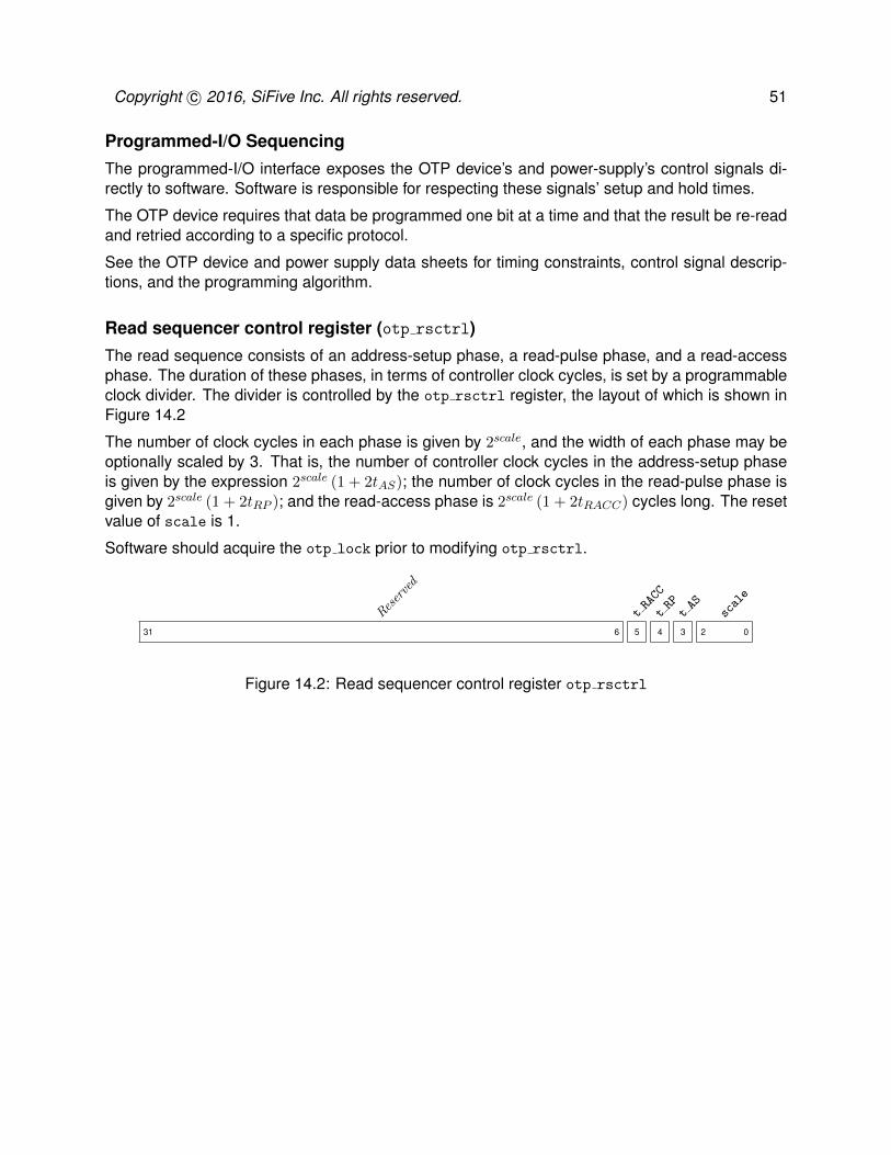
Copyright c© 2016, SiFive Inc. All rights reserved. 51
Programmed-I/O SequencingThe programmed-I/O interface exposes the OTP device’s and power-supply’s control signals di-rectly to software. Software is responsible for respecting these signals’ setup and hold times.
The OTP device requires that data be programmed one bit at a time and that the result be re-readand retried according to a specific protocol.
See the OTP device and power supply data sheets for timing constraints, control signal descrip-tions, and the programming algorithm.
Read sequencer control register (otp rsctrl)The read sequence consists of an address-setup phase, a read-pulse phase, and a read-accessphase. The duration of these phases, in terms of controller clock cycles, is set by a programmableclock divider. The divider is controlled by the otp rsctrl register, the layout of which is shown inFigure 14.2
The number of clock cycles in each phase is given by 2scale, and the width of each phase may beoptionally scaled by 3. That is, the number of controller clock cycles in the address-setup phaseis given by the expression 2scale (1 + 2tAS); the number of clock cycles in the read-pulse phase isgiven by 2scale (1 + 2tRP ); and the read-access phase is 2scale (1 + 2tRACC) cycles long. The resetvalue of scale is 1.
Software should acquire the otp lock prior to modifying otp rsctrl.
Reserved
31 6
tRACC
5
tRP
4
tAS
3
scale
2 0
Figure 14.2: Read sequencer control register otp rsctrl

52 SiFive E300 Platform Reference Manual, Version 1.0.1

Chapter 15
E300 Pulse-Width Modulation (PWM)Peripheral
This chapter describes the operation of the E300 Pulse-Width Modulation peripheral (PWM).
PWM Overview
Figure 15.1 shows an overview of the PWM peripheral. The default configuration described herehas four independent PWM comparators (pwmcmp0–pwmcmp3), but custom configurations with ncmp
comparators are available on request. The PWM block can generate multiple types of waveformon GPIO output pins (pwmXgpio), and can also be used to generate several forms of internal timerinterrupt. The comparator results are captured in the pwmcmpXip flops and then fed to the PLIC aspotential interrupt sources. The pwmcmpXip outputs are further processed by an output gangingstage before being fed to the GPIOs.
The PWM unit can be provided in different comparator precisions up to 16 bits, with the versiondescribed here having the full 16 bits. To support clock scaling, the pwmcount register is 15 bitswider than the comparator precision, cmpwidth.
PWM Memory Map
The memory map for the PWM peripheral is shown in Table 15.1.
PWM Count Register (pwmcount)
The PWM unit is based around a counter held in pwmcount. The counter can be read or writtenover the TileLink bus. The pwmcount register is (15 + cmpwidth) bits wide. For example, forcmpwidth of 16 bits, the counter is held in pwmcount[30:0], and bit 31 of pwmcount returns a zerowhen read.
When used for PWM generation, the counter is normally incremented at a fixed rate then reset tozero at the end of every PWM cycle. The PWM counter is either reset when the scaled counterpwms reaches the value in pwmcmp0, or is simply allowed to wraparound to zero.
The counter can also be used in one-shot mode, where it disables counting after the first reset.
53

54 SiFive E300 Platform Reference Manual, Version 1.0.1
pwmcfgwurst
pwmcount
pwmspwmscale
reseten
pwmz
eroc
mp
pwmdeglitch
carryout
pwmcmp3
pwmcmp3ip>=?pwmcmp3center
pwms[15] 01
pwmcmp3gang pwmcmp3gpio
pwmcmp2
pwmcmp2ip>=?pwmcmp2center
pwms[15] 01
pwmcmp2gang pwmcmp2gpio
pwmcmp1
pwmcmp1ip>=?pwmcmp1center
pwms[15] 01
pwmcmp1gang pwmcmp1gpio
pwmcmp0
pwmcmp0ip>=?pwmcmp0center
pwms[15] 01
pwmcmp0gang pwmcmp0gpio
reset pwmoneshoten
pwmstickyip
Figure 15.1: E300 PWM Peripheral.
PWM Configuration Register (pwmcfg)
pwmcmp3ip
31
pwmcmp2ip
30
pwmcmp1ip
29
pwmcmp0ip
28
pwmcmp3gang
27
pwmcmp2gang
26
pwmcmp1gang
25
pwmcmp0gang
24
Reserved
23 20
pwmcmp3center
19
pwmcmp2center
18
pwmcmp1center
17
pwmcmp0center
16
Reserved
15 14
pwmenoneshot
13
pwmenalways
12
Reserved
11
pwmdeglitch
10
pwmzerocmp
9
pwmsticky
8
Reserved
7 4
pwmscale
3 0
Figure 15.2: PWM configuration register pwmcfg
The pwmcfg register contains various control and status information regarding the PWM peripheral,as shown in Figure 15.2.
The pwmen* bits control the conditions under which the PWM counter pwmcount is incremented.The counter increments by one each cycle only if any of the enabled conditions are true.
If the pwmenalways bit is set, the PWM counter increments continuously. When pwmenoneshot isset, the counter can increment but pwmenoneshot is reset to zero once the counter resets, disablingfurther counting (unless pwmenalways is set). The pwmenoneshot bit provides a way for softwareto generate a single PWM cycle then stop. Software can set the pwnenoneshot again at any time

Copyright c© 2016, SiFive Inc. All rights reserved. 55
Address Description0x00 pwmcfg
0x04 Reserved0x08 pwmcount
0x0C Reserved0x10 pwms
0x14 Reserved0x18 Reserved0x1C Reserved0x20 pwmcmp0
0x24 pwmcmp1
0x28 pwmcmp2
0x2C pwmcmp3
Table 15.1: SiFive PWM memory map, offsets relative to PWM peripheral base address.
to replay the one-shot waveform. The pwmen* bits are reset at wakeup reset, which disables thePWM counter and saves power.
The 4-bit pwmscale field scales the PWM counter value before feeding it to the PWM comparators.The value in pwmscale is the bit position within the pwmcount register of the start of a cmpwidth-bitpwms field. A value of 0 in pwmscale indicates no scaling, and pwms would then be equal to thelow cmpwidth bits of pwmcount. The maximum value of 15 in pwmscale corresponds to dividing theclock rate by 215, so for an input bus clock of 16 MHz, the LSB of pwms will increment at 488.3 Hz.
The value of pwms is memory-mapped and can be read as a single cmpwidth-bit value over theTileLink bus.
The pwmzerocmp bit, if set, causes the PWM counter pwmcount to be automatically reset to zeroone cycle after the pwms counter value matches the compare value in pwmcmp0. This is normallyused to set the period of the PWM cycle. This feature can also be used to implement periodiccounter interrupts, where the period is independent of interrupt service time.
PWM Compare Registers (pwmcmp0–pwmcmp3)
Reserved
31 16
pwmcmp0[15:0]
15 0
Figure 15.3: PWM compare register pwmcmp0. Registers pwmcmp1–pwmcmp3 have the same format.This diagram assumes that cmpwidth of 16. The actual width each register is cmpwidth.
The primary use of the ncmp PWM compare registers is to define the edges of the PWM waveformswithin the PWM cycle.
Each compare register is a cmpwdith-bit value against which the current pwms value is compared

56 SiFive E300 Platform Reference Manual, Version 1.0.1
every cycle. The output of each comparator is high whenever the value of pwms is greater than orequal to the corresponding pwmcmpX.
If the pwmzerocomp bit is set, when pwms reaches or exceeds pwmcmp0, pwmcount is cleared to zeroand the current PWM cycle is completed. Otherwise, the counter is allowed to wrap around.
Deglitch and Sticky circuitryTo avoid glitches in the PWM waveforms when changing pwmcmpX register values, thepwmdeglitch bit in pwmcfg can be set to capture any high output of a PWM comparator in a stickybit (pwmcmpXip for comparatorX) and prevent the output falling again within the same PWM cycle.The pwmcmpXip bits are only allowed to change at the start of the next PWM cycle.
Note the pwmcmp0ip bit will only be high for one cycle when pwmdeglitch and pwmzerocmp areset where pwmcmp0 is used to define the PWM cycle, but can be used as a regular PWM edgeotherwise.
If pwmdeglitch is set, but pwmzerocmp is clear, the deglitch circuit is still operational but is now trig-gered when pwms contains all 1s and will cause a carry out of the high bit of the pwms incrementerjust before the counter wraps to zero.
The pwmsticky bit will disallow the pwmcmpXip registers from clearing if they’re already set, and isused to ensure interrupts are seen from the pwmcmpXip bits.
Generating Left- or Right-Aligned PWM Waveforms
pwms 0 1 2 3 4 5 6 0 1 2 3 4 5 6 0 1
pwmcmpX=3
pwmcmpX=1
pwmcmpX=0
pwmcmpX=2
pwmcmpX=4
pwmcmpX=5
pwmcmpX=6
pwmcmpX=7
PWM Cycle
Figure 15.4: E300 basic right-aligned PWM waveforms. All possible base waveforms are shownfor a 7-clock PWM cycle (pwmcmp0=6). The waveforms show the single cycle delay caused byregistering the comparator outputs in the pwmcmpXip bits. The signals can be inverted at theGPIOs to generate left-aligned waveforms.
Figure 15.4 shows the generation of various base PWM waveforms. The Figure illustrates that ifpwmcmp0 is set to less than the maximum count value (6 in this case), it is possible to generate

Copyright c© 2016, SiFive Inc. All rights reserved. 57
pwms pwmscenter
000 000
001 001
010 010
011 011
100 011
101 010
110 001
111 000
Figure 15.5: Illustration of how count value is inverted before presentation to comparator whenpwmcmpXcenter is selected, using a 3-bit pwms value.
both 100% (pwmcmpX = 0) and 0% (pwmcmpX > pwmcmp0) right-aligned duty cycles using the othercomparators. The pwmcmpXip bits are routed to the GPIO pads, where they can be optionally andindividually inverted thereby creating left-aligned PWM waveforms (high at beginning of cycle).
Generating Center-Aligned (Phase-Correct) PWM Waveforms
The simple PWM waveforms above shift the phase of the waveform along with the duty cycle.A per-comparator pwmcmpXcenter bit in pwmcfg allows a single PWM comparator to generate acenter-aligned symmetric duty-cycle as shown in Figure 15.6 The pwmcmpXcenter bit changes thecomparator to compare with the bitwise inverted pwms value whenever the MSB of pwms is high.
This technique provides symmetric PWM waveforms but only when the PWM cycle is at the largestsupported size. At a 16 MHz bus clock rate with 16-bit precision, this limits the fastest PWM cycleto 244 Hz, or 62.5 kHz with 8-bit precision. Higher bus clock rates allow proportionally faster PWMcycles using the single comparator center-aligned waveforms. This technique also reduces theeffective width resolution by a factor of 2.
pwms 0 1 2 3 4 5 6 7 1 2 3 4 5 6 0 1
pwmcmpX=1
pwmcmpX=0
PWM Cycle
0
pwmcmpX=2
pwmcmpX=3
pwmcmpX=4
Figure 15.6: E300 center-aligned PWM waveforms generated from one comparator. All possiblewaveforms are shown for a 3-bit PWM precision. The signals can be inverted at the GPIOs togenerate opposite-phase waveforms.
When a comparator is operating in center mode, the deglitch circuit allows one 0-1 transition during

58 SiFive E300 Platform Reference Manual, Version 1.0.1
the first half of the cycle, and one 1-0 transition on the second half of the cycle.
Generating Arbitrary PWM Waveforms using GangingA comparator can be ganged together with its next-highest-numbered neighbor to generate arbi-trary PWM pulses. When the pwmcmpXgang bit is set, comparator X fires and raises its pwmXgpio
signal. When comparator X + 1 (or pwmcmp0 for pwmcmp3) fires, the pwmXgpio output is reset tozero.
Generating One-shot WaveformsThe PWM peripheral can be used to generate precisely timed one-shot pulses by first initializingthe other parts of pwmcfg then writing a 1 to the pwmenoneshot bit. The counter will run for onePWM cycle, then once a reset condition occurs, the pwmenoneshot bit is reset in hardware toprevent a second cycle.
PWM InterruptsThe PWM can be configured to provide periodic counter interrupts by enabling auto-zeroing of thecount register when a comparator 0 fires (pwmzerocmp=1). The pwmsticky bit should also be setto ensure interrupts are not forgotten while waiting to run a handler.
The interrupt pending bits pwmcmpXip can be cleared down using writes to the pwmcfg register.
The PWM peripheral can also be used as a regular timer with no counter reset (pwmzerocmp=0),where the comparators are now used to provide timer interrupts.