sic versus si—evaluation of potentials for performance ...sic versus si—evaluation of...
TRANSCRIPT
SiC versus Si—Evaluation of Potentials for Performance Improvement of Inverter and DC–DC Converter Systems by SiC Power Semiconductors
Juergen Biela, Member, IEEE, Mario Schweizer, Student Member, IEEE, Stefan Waffler, Student Member, IEEE,
and Johann W. Kolar, Senior Member, IEEE „This material is posted here with permission of the IEEE. Such permission of the IEEE does not in any way imply IEEE endorsement of any of ETH Zürich’s products or services. Internal or personal use of this material is permitted. However, permission to reprint/republish this material for advertising or promo-tional purposes or for creating new collective works for resale or redistribution must be obtained from the IEEE by writing to [email protected]. By choosing to view this document you agree to all provisions of the copyright laws protecting it.”

2872 IEEE TRANSACTIONS ON INDUSTRIAL ELECTRONICS, VOL. 58, NO. 7, JULY 2011
SiC versus Si—Evaluation of Potentials forPerformance Improvement of Inverter and DC–DCConverter Systems by SiC Power Semiconductors
Juergen Biela, Member, IEEE, Mario Schweizer, Student Member, IEEE, Stefan Waffler, Student Member, IEEE,and Johann W. Kolar, Senior Member, IEEE
Abstract—Switching devices based on wide bandgap materi-als such as silicon carbide (SiC) offer a significant performanceimprovement on the switch level (specific on resistance, etc.)compared with Si devices. Well-known examples are SiC diodesemployed, for example, in inverter drives with high switchingfrequencies. In this paper, the impact on the system-level perfor-mance, i.e., efficiency, power density, etc., of industrial inverterdrives and of dc–dc converter resulting from the new SiC devices isevaluated based on analytical optimization procedures and proto-type systems. There, normally on JFETs by SiCED and normallyoff JFETs by SemiSouth are considered.
Index Terms—AC–DC power converters, DC–DC power con-verters, SiC power semiconductor switches.
I. INTRODUCTION
THE continuous development of improved power semi-conductors is a key enabling factor for propelling the
constantly increasing demand for higher power density (P/V )and higher efficiency (η) in many power-electronic applica-tions. Recently, the technological progress in manufacturingpower devices based on wide bandgap materials, for example,silicon carbide (SiC) or gallium nitride (GaN), has resulted ina significant improvement of the operating-voltage range forunipolar devices and of the switching speed and/or specificon resistance compared with silicon power devices. In [1], thecurrent status of SiC switching devices with respect to specificon resistance, maximal blocking voltage, specific capacitance,etc., is summarized. In Table I, some basic information aboutthe SiC devices is given.
With these new devices, a question arises as to what in-crease in the system-level performance can be achieved bythe improvements obtained at device level. Such performanceindicators include power density and efficiency of the power-electronic converter. In [1], this influence has been investigatedfor single-phase power-factor correction (PFC) systems. More-over, the demand on the system level has been transferred to adesired profile for the semiconductors, which is compared withthe performance offered by the new SiC devices.
Manuscript received January 29, 2010; revised May 28, 2010 and July 27,2010; accepted August 16, 2010. Date of publication September 2, 2010; dateof current version June 15, 2011.
The authors are with ETH Zurich, 8092 Zürich, Switzerland (e-mail:[email protected]).
Color versions of one or more of the figures in this paper are available onlineat http://ieeexplore.ieee.org.
Digital Object Identifier 10.1109/TIE.2010.2072896
TABLE ICURRENT STATUS OF RELATIVELY MATURE SiC SWITCHES. SINCE THE
ALLOWED DRAIN CURRENT ID DEPENDS SIGNIFICANTLY ON THE
COOLING CONDITIONS, THE VALUES SHOULD JUST GIVE A HINT ON THE
CAPABILITIES OF THE RESPECTIVE SWITCH FOR OPERATION AT HIGHER
JUNCTION TEMPERATURES (125 ◦C OR HIGHER). THE (SPECIFIC) ON
RESISTANCE IS GIVEN FOR 25 ◦C. THE Si IGBT AND THE Si DIODE
ARE PART OF THE FP15R12W1T4 MODULE BY INFINEON
In the area of low-voltage motor drives, numerous papersabout the comparison of Si insulated-gate bipolar transistor(IGBT) and SiC switching devices—mainly SiC JFETs–havebeen published. Here, usually, the Si devices in matrix convert-ers [2], [3] or standard inverters [4], [5] are replaced by SiCdevices, and the change in the system performance is evalu-ated. Depending on the operating point and the switching fre-quency [3], the SiC devices facilitate a significant performanceimprovement—particularly regarding the switching loss. Thisis due to the lack of diode reverse recovery and IGBT tailcurrent which are observed in Si devices. The conduction lossof the SiC devices depends on the chip area since the applieddevices are all unipolar ones. Consequently, the efficiencycomparison is also dependent on the considered chip areas.
The lower switching loss of the SiC devices and the relatedfreedom of being able to increase the switching frequency doesnot influence the achievable power density of standard voltage-source inverter except for the cooling system, which could bereduced when the losses are lower. However, the higher possible
0278-0046/$26.00 © 2010 IEEE

BIELA et al.: SiC VERSUS Si—EVALUATION OF POTENTIALS FOR PERFORMANCE IMPROVEMENT 2873
Fig. 1. Schematic of a two-level inverter for low-voltage standard motordrives.
switching frequencies at low switching loss are advantageousfor dc–dc converter systems since they allow reducing thesize of the inductor and/or transformer [6]. This is particularlytrue at medium-voltage levels [7], [8] where fast switchingdevices based on silicon are nonexistent and where new andultraefficient converter systems are required for future energy-distribution networks [9].
Because in the literature, usually, only a pure replacementof the switching devices by SiC ones and no optimization/adoption of the operating points to the new devices has beenpresented, in Section II, first, the influence of the SiC devices onindustrial inverter drives is investigated. Here, the link betweenthe demands on the system level and the resulting requiredprofile of the switching elements is also discussed. There-after, dc–dc converter systems are considered in Section III,where medium voltage dc–dc converters for future energy-distribution systems are also included. Here, the new switchingdevices based on wide bandgap materials offer a tremendousperformance improvement compared with the state-of-the-artSi technology. In all considerations, a limitation of the junctiontemperature below 175 ◦C and the data of the SiC switchespresented in Table I is assumed. Furthermore, the comparisonis always based on the chip area and not on the current rating ofthe devices provided in the datasheets of the manufacturers asthe chip area is proportional to the costs, and the current ratingsare very much dependent on the application, the switchingfrequency, and the cooling conditions.
II. INVERTER
Low-voltage (< 1000 V) industrial drives are an importantpower-semiconductor application area. Here, mainly two-levelinverters operating at switching frequencies in the range of 4 to16 kHz and at a dc-link voltage in the range of 600 V are used(cf., Fig. 1). In niche applications, matrix converters offeringbidirectional power flow and three-level converters for higheroperating frequencies can also be found.
Due to the high winding inductance of the motors, there isgenerally no need for higher operating frequencies, as shownin Fig. 2(a), except for special high-speed applications, wherethe fundamental frequency is significantly higher than 50 Hz,and the inductance values usually decrease. Also, there is nospecial need for higher kilowatts per kilogram and/or extremepower densities in most applications. Only, in integrated motordrives, a higher power density would be desirable, but in thisapplication, with an improved cooling system, the requirements
Fig. 2. (a) Radar chart of the system requirements for low-voltage industrialdrives where the current status is shown in blue (= 100%), and the desiredvalues are shown in red. Based on the system requirements, the radar chartin (b) for the switching devices is derived, where the current status withsilicon devices (= 100%) is shown in blue, the requirements on the switchlevel are shown in yellow, and the offered performance of SiC devices isshown in red. The numbers are based on the prototype system presented in[10]. (a) System level requirements. (b) Component level requirements andperformance.
often can be met. Since the efficiency of the standard invertersis already quite high and substantially exceeds the efficiencyof the motor, there is (generally speaking) no further require-ment for increased efficiency in comparison with silicon-basedconverters.
A major driving force is the cost, where a significant reduc-tion could result in a more widespread application of inverterdrives. In some areas, a higher reliability is also required,which, however, is difficult to meet with high-temperatureoperation/devices.
The system requirements are translated to the switch level inFig. 2(b), where the current status for silicon devices is shownas reference level (= 100%) in blue, the resulting requirementsare shown in yellow, and the performance achievable withSiC devices is shown in red. Here, it could be seen that theachievable switching speed of SiC and even of Si devices isnot required. Often, even the Si IGBTs are slowed down inorder not to damage the motor-winding isolation/bearings withhigh dv/dt values and to reduce electromagnetic interference(EMI). Also, the high breakdown voltages and the high possiblejunction temperature of SiC are not required in low-voltage

2874 IEEE TRANSACTIONS ON INDUSTRIAL ELECTRONICS, VOL. 58, NO. 7, JULY 2011
TABLE IISPECIFICATIONS OF THE INVERTER SYSTEM
drives. Only the better conductivity of SiC, resulting in asmaller chip area, and the higher achievable efficiency could bebeneficial for inverter systems, in case the costs do not increase.Here, the high costs for SiC devices are a significant limit at themoment.
After the more general remarks, the effect of SiC devices ona real prototype system with the specification given in Table IIare discussed. Here, the following scenarios are considered.
1) How much chip area is required for achieving an effi-ciency of 98.3%?
2) How much chip area is required for keeping the powerdensity constant at 25 kW/dm3 (considering just thecooling system)?
3) How much chip area is required for an ultraefficientdrive with an efficiency of 99.3%, i.e., 1% more than theprototype system?
In addition to the silicon IGBTs with Si-/SiC diodes, the1.2-kV JFETs and MOSFETs as listed in Table I are alsoconsidered.
In Fig. 3, the results of the mentioned scenarios are shown.The results are based on some simplifying assumptions. First,it has to be noticed that only pure silicon performance hasbeen analyzed, so additional losses of fans or digital controlelectronics will not be considered. The conduction loss ismodeled with a typical simplified device behavior, namely
PCond,IGBT(I) =Vf,T · I + Ron,T · I2 (1)PCond,Diode(I) =Vf,D · I + Ron,D · I2 (2)PCond,JFET(I) =RDS(on),J · I2 (3)
PCond,MOSFET(I) =RDS(on),M · I2. (4)
The parameters are dependent on the junction temperature.For the bidirectional JFET and MOSFET devices, the losscharacteristic in the forward and reverse current directions isassumed to be the same. With a low switching frequency of4 kHz, the switching losses of JFET and MOSFET are muchlower than the conduction losses and will be neglected. Theswitching losses of the IGBT and diode are modeled with theswitching energies linearly scaled [11]
EOn,T (V, I) =EOnT,nom · V
Vnom· I
Inom(5)
EOff,T (V, I) =EOffT,nom · V
Vnom· I
Inom(6)
Fig. 3. Chip area of the 1.2-kV SiCED JFET, the 1.2-kV SemiSouth JFET,the 1.2-kV Cree MOSFET, and a Si IGBT with Si and with SiC diode for threedifferent cases: (a) All systems have an efficiency of 98.3%, (b) all systems havea volume of 0.3 dm3, and (c) the chip area required for an efficiency increaseof 1%, i.e., for 99.3%.
EOn,D(V, I) = 0 (7)
EOff,D(V, I) = EOffD,nom · V
Vnom· I
Inom. (8)
BIELA et al.: SiC VERSUS Si—EVALUATION OF POTENTIALS FOR PERFORMANCE IMPROVEMENT 2875
The nominal values are taken from datasheet values of the latestgeneration IGBT from Infineon (1.2 kV, 15 A) with parametersas listed in Table I. For the implementation variant with SiCantiparallel diodes, the diode turn-off energy is assumed tobe zero, and the IGBT turn-on energy is assumed to be 30%smaller due to the missing diode reverse-recovery effect.
The device losses of the inverter system are calculated ana-lytically for a symmetric space-vector modulation strategy. Thewell-known results for the average conduction and switchinglosses will not be repeated here but could be found in [11] and[12]. In a further step, the on resistances of all devices are madearea dependent (cf., [13]) with the generic formula
ROn = ROn,nom · AChip,nom
AChip. (9)
For the dependence of the switching energies on the die size,no general trend could be observed. They are assumed to stayconstant for the considered chip-area range.
In a same way, the thermal resistance Rth,J−S for eachdevice is made area dependent. The nominal value of theresistance of 30 K/(W · mm2) was fitted with a datasheet studyin [13] and is used for all dies independent of technology
Rth,J−S =Rth,J−S,Anom
AChip. (10)
Finally, a forced-air cooling system with a cooling-systemperformance index (CSPI) of 15 W/(K · dm3) is assumed. Thisallows for complete inclusion of the thermal model into theoptimization process
Rth,S−A =1
CSPI · VolHS. (11)
The heat-sink temperature can be calculated with the totallosses of the inverter system
THS = TAmb + PTotal · Rth,S−A. (12)
The junction temperature of each chip die is given by
TJ,Die = THS + PAVG,Die · Rth,J−S . (13)
Now, the set of equations can be solved for the differentscenarios defined previously. For each scenario, the junctiontemperature is assumed to be 175 ◦C. This implies that thefundamental output frequency is high so that average devicelosses can be used, and no time behavior of the thermal modelhas to be considered.
For a fixed efficiency, the formulas directly lead to the chipareas and size of the necessary heat sink. For the IGBT withantiparallel diodes, the chip size of the diode is assumed to behalf of the IGBT chip size in order to reduce by a degree offreedom.
Due to the reverse-recovery losses of the internal diodes ofthe SiC JFETs and the SiC MOSFETs, antiparallel Schottkydiodes are assumed, which only conduct shortly during theinterlocking delay. For the rest of the time, the current is flowingin reverse direction through the channel of the unipolar device.Consequently, the area of the SiC diodes could be relatively
small and is assumed to be 50% of the SiC diode area of theIGBT+SiC diode combination.
It is interesting to note that for a constant ambient temper-ature (e.g., 25 ◦C), the equations define a minimum efficiencyfor which a cooling solution exists. If the efficiency is chosento be lower than this minimum, the resulting chip dies are sosmall that the temperature drop from the junction to the sinkgets higher than the maximal 150 ◦C, and the heat-sink sizegrows to infinity.
For a fixed heat-sink size, the formulas directly lead tothe necessary chip sizes and the resulting inverter efficiency.Finally, the increase in area for a high-performance 99.3%inverter efficiency (pure silicon) is calculated. It can be notedthat the chip area of IGBT and diode has to be increased tounrealistic values, showing the advantages of SiC JFETs andMOSFETs for ultrahigh efficiency motor drives.
The higher efficiency achievable with SiC devices is, forexample, very interesting for renewable energy conversion(photovoltaic inverter) where a special focus is put on effi-ciency. There, the higher costs of the SiC devices could becompensated by saved energy. In general, however, it is notimportant if the losses are saved at the generator or at the con-sumer side—except for the losses due to energy transmission/distribution.
In automotive industry, in addition to efficiency, a higherpossible operating temperature is also advantageous due tohigh ambient temperatures if the power-electronic converter ismounted close to a combustion engine. There, the remainingcomponents, e.g., capacitors, control electronics, or gate drives,are the limiting factors in addition to reliability issues. Further-more, with a water cooler, a smaller footprint of the SiC deviceswould also be advantageous with respect to costs.
Higher possible junction temperatures could also improve therobustness of the converter systems in case of overload situa-tions. Replacing the Si bipolar devices with fast SiC unipolarswitches also requires considering the parasitics in the layoutand the mechanical design more carefully due to fast switchingtransients.
III. DC–DC CONVERTER
The second application area considered in this paper is thedc–dc converter, which is split as low-voltage converter—nonisolated and isolated—and high-voltage isolated dc–dc con-verter, which will be discussed next. However, the generalrequirements for low voltage dc–dc converter in telecommu-nication and in automotive applications are evaluated based onthe net diagrams shown in Fig. 4.
The most important issue on the system level is cost since,in both areas, there is quite a high cost pressure and a verycompetitive market. In the automotive area, the weight of theconverter and the power density are also important criteria sincethe first directly influences the fuel efficiency, and the secondresults from the limited available space. The latter is also truefor telecommunication systems, as the costs of floor space arehigh. Also, for both application areas, the efficiency has becomemore and more important in the last years due to rising energycosts and environmental concerns, which is particularly true for

2876 IEEE TRANSACTIONS ON INDUSTRIAL ELECTRONICS, VOL. 58, NO. 7, JULY 2011
Fig. 4. Radar charts of the system and component level requirements fornonisolated dc–dc converter. Here, the numbers show typical values for thesystem shown in Fig. 7. (a) System level requirements. (b) Component levelrequirements and performance.
renewable energies and energy storage [14]. In particular, inthe automotive area, with its harsh environmental conditions(e.g., vibrations, temperature), the reliability should be veryhigh, which is difficult particularly if one thinks of high-temperature operation. Reliability is also an important issue intelecommunication supplies as shutdown of a data center is veryexpensive.
These system-level criteria result in the requirements for theswitches, as shown in Fig. 4(b), where the current status isshown as reference value (= 100%) and where the achievableperformance of SiC devices and the demands on switches inthe automotive and the telecommunication area are also given.There, mainly, the higher conductivity per area of SiC devicesand the higher junction temperature for automotive applica-tions meet the demands. Higher blocking-voltage capabilityand improved switching performance are not required sincethe operating voltages are usually limited to a few hundredvolts and soft switching could be achieved with very smalladditional effort. As with the other applications, the highercosts of SiC devices are a major drawback, and this signifi-cantly limits the area of the SiC devices which could be usedat the same cost level, which influences the achievable sys-tem performance—particularly, efficiency. The two low-voltagesystems considered now support this statement.
Fig. 5. Bidirectional buck–boost converter with specifications given inTable III for automotive applications.
TABLE IIISPECIFICATIONS OF THE AUTOMOTIVE DC–DC
CONVERTER SHOWN IN FIG. 7
Fig. 6. Waveforms of the primary and secondary voltage and the inductorcurrent.
A. Low-Voltage Converter
1) Nonisolated Automotive DC–DC Converter: First, adc–dc converter without galvanic isolation is considered. Atypical application area of such a converter is hybrid electricalvehicles or fuel-cell vehicles, where the converter is usedfor power management between the batteries, supercapacitors,and/or fuel cells [15], [16]. In these systems, a bidirectionalpower flow for providing energy during acceleration and storingenergy during braking is often required.
A converter for this application has to meet the prevalentautomotive requirements, such as being a low-cost design, andminimize the component size and count. This can be achievedby increased switching frequency and interleaved operation ofmultiple converter phases. Fixed-frequency operation is desireddue to EMI restrictions, and a highly compact design and a lowoverall weight are required.
In Fig. 5, a schematic of the considered bidirectional dc–dcconverter consisting of four switches, an inductor, and twocapacitors is shown. The specifications of the converter are
BIELA et al.: SiC VERSUS Si—EVALUATION OF POTENTIALS FOR PERFORMANCE IMPROVEMENT 2877
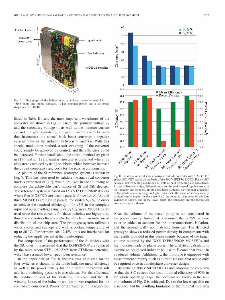
Fig. 7. Photograph of the bidirectional buck–boost converter with 150 . . .450-V input and output voltages, 12-kW nominal power, and a switchingfrequency of 100 kHz.
listed in Table III, and the most important waveforms of theconverter are shown in Fig. 6. There, the primary voltage v1
and the secondary voltage v2 as well as the inductor currentiL and the gate signals Sν are given, and it could be seenthat, in contrast to a normal buck–boost converter, a negativecurrent flows in the inductor between t3 and TP . With thisspecial modulation method, a soft switching of the convertercould simply be achieved by control, and the efficiency couldbe increased. Further details about the control method are givenin [17], and in [18], a similar structure is presented where thechip area is reduced by using snubbers, which however increasethe circuit complexity and costs for the passive components.
A picture of the Si reference prototype system is shown inFig. 7. This has been used to validate the analytical convertermodels presented in [19], which are used in the following tocompare the achievable performance of Si and SiC devices.The reference system is based on IXYS IXFB82N60P deviceswhere four MOSFETs are used in parallel for switch S1/S3 andthree MOSFETs are used in parallel for switch S2/S4, in orderto achieve the required efficiency of ≥ 95% in the completeinput and output voltage range. For S1/S3, more MOSFETs areused since the rms currents for these switches are higher and,thus, the converter efficiency also benefits from an unbalanceddistribution of the chip area. The prototype system utilizes awater cooler and can operate with a coolant temperature ofup to 80 ◦C. Furthermore, six 12-kW units are interleaved forreducing the ripple current at the input/output.
For comparison of the performance of the Si devices withthe SiC ones, it is assumed that the IXFB82N60P are replacedby the more recent STY112N65M5 from STMicroelectronics,which have a much lower specific on resistance.
In the upper half of Fig. 8, the resulting chip area for thefour switches is shown. In the lower half, the mean efficiencyas well as the power density for the different considered softand hard switching systems is also shown. For the efficiency,the conduction loss of the switches, the core, and the HFwinding losses of the inductor and the power required for thecontrol are considered. Power for the water pump is neglected.
Fig. 8. Calculation results for a nonisolated dc–dc converter with Si MOSFETand/or SiC JFET scaled on the basis of the 500-V JFET by SiCED. For the SiCdevices, soft-switching conditions as well as hard switching are considered.In case of hard switching, different limits for the peak-to-peak ripple current inthe inductor are assumed. In all considered systems, the minimal efficiencyin the whole operating range is higher than 95%; the mean efficiency usuallyis significantly higher. In the upper half, the required chip areas of the fourswitches is shown, and in the lower graph, the efficiency and the theoreticalpower density are shown.
Also, the volume of the water pump is not considered inthe power density. Instead, it is assumed that a 25% volumemust be added to account for the interconnections, isolation,and the geometrically not matching housings. The depictedprototype shows a reduced power density in comparison withthe results provided in this paper mainly because of the largervolume required by the IXYS IXFB82N60P MOSFETs andthe inductor made of planar cores. The analytical calculationsassume an optimized inductor built with E-cores that result ina reduced volume. Additionally, the prototype is equipped withmeasurement circuitry, such as current sensors, that would onlybe required once in a multiphase converter design.
By utilizing 500-V SiCED JFETs and adapting the chip areaso that the SiC system also has a minimal efficiency of 95% inthe whole operating range, the performance shown in the sec-ond column of Fig. 8 is achieved. Due to the lower specific onresistance and the resulting limitation of the minimal chip area

2878 IEEE TRANSACTIONS ON INDUSTRIAL ELECTRONICS, VOL. 58, NO. 7, JULY 2011
Fig. 9. Phase-shift dc–dc converter with current doubler output. (a) 5-kWprototype of the proposed 400 V/48 . . . 54 V dc–dc converter: Height:1 U, volume: 0.56 dm3, power density: 147 W/in3 (9 kW/dm3). (b) Circuitschematic of the phase-shift full-bridge converter with current-doubler rectifier.
by thermal constraints, the mean efficiency of the SiC system isslightly higher. Also, the power density increases slightly dueto the reduced volume required for the semiconductors.
In the third, fourth, and fifth column, the results for op-eration under hard-switching conditions with 500-V SiCEDJFETs are shown. Here, different limits for the peak-to-peakripple currents have been assumed, which results in a smallerinductance value if the ripple is larger. This also increases thepower density of the system. In case of a 95% ripple, i.e.,almost discontinuous operation, the power density becomesmaximal. Here, the value and the volume of the boost inductoris larger as in the case of the soft-switched systems, but thevolume reduction due to much smaller required chip area (i.e.,also smaller cooling system) outweighs this. A relatively lowdependence of the chip area on the ripple current in the case ofthe hard-switched system results since the rms current does notdepend so much on the current ripple but on the dc componentof the current. Furthermore, the efficiency is slightly higherthan the desired 95% since the chip area is limited by thermalconstraints so that the RDSon is smaller than necessary.
In the case of soft-switching conditions, with SiC, the chiparea could be reduced to approximately 60% of the Si chip area.
In the calculations performed for evaluating the performanceof the different devices, for the inductor, an E-core with airgap made of N87 material, a maximal flux density of Bmax =0.3 T, and a maximal temperature of TL = 100 ◦C has beenassumed. For the winding, litz wire is used, and the currentdensity is limited to 5 A/mm2. Further details on the inductoroptimization can be found in [19].
TABLE IVSPECIFICATIONS FOR THE PROPOSED IT DC–DC CONVERTER
Fig. 10. Waveforms of the primary current and voltage of the current-doublerrectifier at nominal power operating with phase-shift modulation.
2) Isolated DC–DC Converter: A large market for isolateddc–dc converter in the kilowatt range is the telecommunicationpower supply, where often, full-bridge converters with softswitching or some kind of resonant converters are applied.These converter types meet the demands for high-power densityand high efficiency—an issue which became more and moreimportant due to rising energy costs. However, since initialcosts are very important, usually relatively simple and robustdesigns are applied.
In Fig. 9, the circuit schematic and a photograph of afull-bridge converter with current doubler, which fulfills theserequirements, are shown, and in Table IV, the specificationsof the converter are given. The design of the converter isbased on an optimization algorithm, which also includes thethermal and the electromagnetic design of the converter besidesthe electrical model. Further details on the design and theoptimization procedure can be found in [20] and on the thermaldesign in [21]. The converter has been built for validating themodels and is based on 500-V MOSFETs APT50M72B2 fromMicrosemi.
In Fig. 10, the basic waveforms for the primary currentand the primary voltage are given. Due to the leakage induc-tance Lσ of the transformer and the phase-shift modulation,all four switches operate under zero-voltage-switching (ZVS)condition, resulting in negligible switching loss at a very low

BIELA et al.: SiC VERSUS Si—EVALUATION OF POTENTIALS FOR PERFORMANCE IMPROVEMENT 2879
Fig. 11. Efficiency and power density for the isolated dc–dc converter with Si MOSFETs (STY112N65M5) and/or the 500-V JFETs for the cases where the SiCchip area is scaled so that the converters have the same efficiency η or the same power density P/V and for the case where the chip area of the SiC devices is1/5 (ASiC = 1/5ASi). For the SiC devices, a 140 ◦C and a 165 ◦C limit for the junction temperature and separate heat sinks for the Si rectifier diodes and theswitches of the full-bridge have been assumed. Below the graph, the temperature THS,SW of the heat sink for the switch and THS,Dio for the heat sink of therectifier diodes are shown. The switching losses, which are relatively low, are evaluated based on measurements with the Si MOSFET and are assumed to be inthe same range for the SiC devices.
effort on the circuit and control side. Consequently, only theconduction loss and therewith the on resistance of the switchesis interesting. For achieving ZVS conditions and zero switchingloss, the switches require a minimum output capacitance, whichdepends on the switching speed. With a smaller capacitancevalue, the switching loss increase, but it can also help toincrease part of the load efficiency.
In spite of the negligible switching losses, the optimalswitching frequency of the converter which results in maximalpower density is just 200 kHz. Increasing the frequency willresult in a smaller power density and efficiency as explainedin [22]. There, it is also shown that for achieving a maximalefficiency of the considered converter systems, the switchingfrequency must be lower than the mentioned 200 kHz.
Based on the optimization procedure, the full-bridge con-verter has been optimized with the data of the 650-V MOSFETSTY112N65M5 from ST on the silicon side and of the 500-Vnormally on JFET from SiCED on the SiC side. Here, thefollowing assumptions have been made:
1) core material: N87 from EPCOS (Tmax ≤ 115 ◦C);2) windings: Foil windings (Tmax ≤ 125 ◦C);3) center-tapped secondary winding;4) rectifier diode: APT100S20 from Microsemi;5) CSPI: 23 (for transformer and semiconductor heat sink);6) maximum junction temperature Tj,max ≤ 140 ◦C for Si
MOSFET;7) maximum junction temperature Tj,max ≤ 140/165 ◦C for
SiC JFET.Fig. 11 shows the results for the cases where the chip area
is adapted so that the efficiency and/or the power density is thesame for the Si- and the SiC-based converters and for the casewhere the chip area of the SiC devices is fixed to a fifth of theSi MOSFET. In all cases, the results for a junction temperature
limit of the SiC JFET of 140 ◦C and 165 ◦C are shown, andit is assumed that the switches of the full-bridge converterare mounted on a different heat sink from that of the outputrectifier diodes. With a junction temperature limit of 165 ◦C,the heat-sink temperature reaches a peak temperature of160 ◦C, which requires a thermal isolation between the heatsink and the other components. In general, the heat-sink tem-perature is relatively close to the junction temperature in anoptimized design since the thermal resistance between thejunction and heat sink is relatively small. Consequently, with ajunction temperature limit of 165 ◦C, the heat-sink temperatureis also high.
The calculated peak-power density of 17.7 kW/dm3 also hasto be considered against the background of the high heat-sinktemperature because a thermal isolation is not included in thepower-density calculation so that in the real system, the powerdensity might be lower. Basically, it is important to note that inthe power density, only the net component volume is included,i.e., the power density decreases to roughly 2/3 (for systemswithout thermal isolation) in the final system due to the air inbetween the components required for insulation and due to thegeometrically not matching housings of the components.
For achieving the same efficiency with SiC devices as withthe Si MOSFET, approximately 43%–54% of the chip area isrequired for the SiC JFET. Due to the high heat-sink temper-ature, the size of the cooling system decreases, and therefore,the power density increases to 17.7 kW/dm3 for a junctiontemperature limit of 165 ◦C.
The same power density could be achieved if the SiC deviceshave 30%–40% of the Si MOSFET chip area. Here, with alower junction temperature, approximately the same efficiencycould be achieved with the SiC devices as the on resistanceincreases with junction temperature.

2880 IEEE TRANSACTIONS ON INDUSTRIAL ELECTRONICS, VOL. 58, NO. 7, JULY 2011
Fig. 12. Schematic of a Super Cascode consisting of six series-connectedSiC JFETs and a silicon low-voltage MOSFET. At 5 kV, 5 A, and 25 ◦C, theSuper Cascode has approximately 3.3-mJ turn-on losses, which decrease almostlinearly to 1.2 mJ for 0 A. Due to the phase-shift operation, the turn-off lossesare negligible [27].
B. High-Voltage Converter
The benefit of SiC devices in low-voltage applications isbasically limited to some efficiency and/or power densityincrease–depending on the topology/application to a greateror lesser extent. However, with SiC devices, no major newapplication area is enabled except for environments with highambient temperature. Moreover, the high costs of SiC devicesand the new processing technology required for SiC often willconstrict the application of the new devices to low-voltagesystems.
Considering medium-voltage levels where new applications,for example, in future energy distribution, are emerging [23],[24], SiC devices could offer a functionality and performancewhich are not achievable with Si devices. In [25], for example, a5-kV to 700-V isolated bidirectional dc–dc converter operatingat 50 kHz is presented, which shows outstanding efficiency andpower density enabled by the performance of SiC devices. Theconverter is based on the dual active bridge topology, whichhas soft-switching conditions, bidirectional power flow, and arelatively simple control [26].
On the 5-kV side, a cascode connection of normally on1.2-kV JFETs and a low-voltage (40 V) Si MOSFET, as shownin Fig. 12 (a Super Cascode), is used. With this configuration,a blocking voltage of 6 × 1.2 kV = 7.2 kV and very fasttransients, as presented in [27], can be achieved. The voltagebalancing of the JFETs is inherently achieved with avalanchediodes and additional small RC networks so that the wholeSuper Cascode could be controlled just via the gate of the Si-MOSFET and basically operates like a single switch.
The conduction losses in the dc–dc converter can simply bedecreased by increasing the chip size of the JFETs and theMOSFET, and efficiencies in the range of 99% are possiblewith the SiC JFETs. Due to the ZVS operation, the high-
Fig. 13. (a) Turn-on and (b) turn-off switching transients of 6.5-kV JFETsin cascode connection operating as half bridge with ohmic load. The switchesshow outstanding transient performance enabling new converter concepts in themedium-voltage range.
operating frequency is possible, resulting in a very compactand low weight design. This could be, for example, veryadvantageously used in wind generators where the weight ofthe power-electronic conversion system directly influences thecosts and size of the mechanical design of the tower/nacelle.
In the future, the operating voltage level of the Super Cascodewill increase further, for example, by applying 6.5-kV JFETs.In Fig. 13, measurement results of such JFETs operating ina half-bridge connection are shown. Based on these, a SuperCascode with operating voltages of more than 20 kV will bepossible, which will enable new converter concepts in thisvoltage range.
In addition to the semiconductors, other issues, e.g., thetransient voltage distribution in the magnetic components,the packaging, and the low inductive/capacitive design meet-ing the requirements for high insulation voltages must alsobe solved before fast, ultracompact, and efficient SiC-basedpower-electronic converter systems in the voltage range higherthan 10 kV will be available. However, with the functionalityof such systems, the energy distribution and integration offluctuating renewable energy sources will significantly changein the future.
IV. CONCLUSION
Considering low-voltage inverter drives limited to a fewkilohertz switching frequency, the SiC switching devices do

BIELA et al.: SiC VERSUS Si—EVALUATION OF POTENTIALS FOR PERFORMANCE IMPROVEMENT 2881
not offer a performance boost compared with Si IGBTs, as arelatively high SiC chip area is required in order to achieve thesame system performance as with Si. Just as with ultrahigh ef-ficient drive systems (> 99%) with SiC devices, a significantlysmaller chip area is required as the unipolar devices allow an ap-proximately linear conduction-loss reduction by increasing thechip area. This high efficiency could be advantageously usedin converter systems for renewable energy e.g., photovoltaic,where the high costs of SiC will pay back to reduced losses andlong operating time. In automotive industry, the higher possiblejunction temperature could be advantageous due to increasedambient temperatures if the converter is mounted close to acombustion engine. Furthermore, with SiC chips, a smallerfootprint of the modules is possible.
In the area of low-voltage dc–dc converter where, very often,soft-switching conditions can be achieved with very low effort,SiC devices mainly offer the possibility of reducing the chiparea for a desired efficiency. This could help to increase thepower density as has been shown using the example of thenonisolated bidirectional buck–boost converter, where the chiparea approximately could be reduced to 50% for achievingthe same performance with SiC devices. Also, for isolateddc–dc converter for which a phase-shift converter with current-doubler rectifier has been evaluated in this paper, the mainbenefit is an improvement of power density and/or efficiencyor the reduction of the chip area to approximately 35% at thesame performance. Here, however, the costs of the SiC devicesplay an important role since these benefits often can be realizedby significantly increasing the costs of the semiconductors. Thismight change in the future if the price of SiC devices drops.
In the future, the SiC devices could show a significantadvantage compared with unipolar Si devices if the outputcapacitance of the SiC switches could be reduced significantly,as shown in [28], for GaN devices. This would reduce theswitching losses in hard-switched applications resulting in abetter efficiency and/or a more compact design.
Considering higher power levels and voltages in the medium-voltage-level range, the picture changes substantially since inthis area, SiC devices offer a function and a performancewhich are not achievable with Si devices. In this paper, a 5-kVdc–dc converter operating at 50 kHz with an efficiency ofapproximately 99% is discussed. Such converters will play asignificant role in the future (renewable) energy distribution andwill allow a significant performance boost.
Also, in applications, e.g., accelerators or pulsed-power con-verters for medical systems, where a high output voltage isrequired, high-voltage SiC diodes offer a significant advantageas these enable a reduction of the total voltage drop across therectifier, resulting in lower losses.
In particular, in such a high-voltage system and also inthe considered low-voltage converters, passive components,isolation issues, and converter design must not be neglectedsince these often limit the system performance as much as theswitches do. A good example are motor drives, where the dv/dtoften must be reduced, even with the application of standardIGBTs, in order not to harm the isolation of the windings or tolimit capacitive charging currents.
The results for the different systems could be summarized asshown in Fig. 14, where a clear performance improvement with
Fig. 14. Nowadays, SiC devices offer only a small performance improvementwith respect to efficiency/power density in the lower operating-voltage rangecompared with current Si MOSFETs. With increasing operating voltages, theperformance improvement increases significantly, particularly as there are onlybipolar Si switching devices available which are relatively slow. The maximalpossible operating temperature of SiC devices is significantly higher than thatof the Si devices.
SiC devices is shown at higher operating-voltage levels and nounipolar Si devices are available. With current SiC devices,there is no significant performance improvement comparedwith unipolar Si devices, and, considering the costs, SiC deviceshave a clear disadvantage as the reduction of chip area isrelatively small compared with the cost ratio between Si andSiC. This is also confirmed by the results which are presented in[1] for a single-phase PFC converter where some of the JFETsby SiCED show a lower performance than the Si switches, andonly the JFETs by SemiSouth show a slight improvement from99.09% to 99.14% efficiency. Therefore, it is also importantto bear in mind that the SiC devices are relatively young anddefinitely will improve significantly in the future.
In addition to SiC, other wide bandgap materials, for ex-ample, GaN also shows interesting material properties andtheoretically enables a tremendous reduction of the specificon resistance, which has an even lower theoretical limit thanSiC. The GaN devices have a lower gate charge, and theoutput capacitance is also smaller [28], which reduces switch-ing losses mainly in hard-switched applications. Furthermore,the processing of the material is simpler and might allow afaster decrease of production costs than is possible with SiC[29], [30].
REFERENCES
[1] J. Biela, M. Schweizer, S. Waffler, B. Wrzecionko, and J. W. Kolar, “SiCvs. Si—Evaluation of potentials for performance improvement of powerelectronics converter systems by SiC power semiconductors,” in Proc. Int.Conf. Silicon Carbide Related Mater., 2009, pp. 1101–1106.
[2] D. Domes, W. Hofmann, and J. Lutz, “A first loss evaluation using avertical SiC-JFET and a conventional Si-IGBT in the bidirectional matrixconverter switch topology,” in Proc. Eur. Conf. Power Electron. Appl.,2005, pp. P.1–P.10.
[3] T. Friedli, S. D. Round, and J. W. Kolar, “A 100 kHz SiC sparsematrix converter,” in Proc. IEEE Power Electron. Spec. Conf., 2007,pp. 2148–2154.
[4] R. Lai, Y. Pei, F. Wang, R. Burgos, D. Boroyevich, T. A. Lipo,V. Immanuel, and K. Karimi, “A systematic evaluation of ac-fed convertertopologies for light weight motor drive applications using SiC semicon-ductor devices,” in Proc. IEEE IEMDC, 2007, vol. 2, pp. 1300–1305.
[5] H.-R. Chang, E. Hanna, and A. V. Radun, “Development and demonstra-tion of silicon carbide (SiC) motor drive inverter modules,” in Proc. IEEE34th Annu. Power Electron. Spec. Conf., 2003, vol. 1, pp. 211–216.
[6] A. M. Abou-Alfotouh, A. V. Radun, H.-R. Chang, and C. Winterhalter,“A 1-MHz hard-switched silicon carbide dc-dc converter,” IEEE Trans.Power Electron., vol. 21, no. 4, pp. 880–889, Jul. 2006.

2882 IEEE TRANSACTIONS ON INDUSTRIAL ELECTRONICS, VOL. 58, NO. 7, JULY 2011
[7] J. Wang, J. Li, X. Zhou, T. Zhao, A. Q. Huang, R. Callanan, F. Husna, andA. Agarwal, “10 kV SiC MOSFET based boost converter,” in Proc. IEEEInd. Appl. Soc. Annu. Meeting, 2008, pp. 1–6.
[8] L. Yang, T. Zhao, J. Wang, and A. Q. Huang, “Design and analysis of a270 kW five-level dc/dc converter for solid state transformer using 10 kVSiC power devices,” in Proc. IEEE Power Electron. Spec. Conf., 2007,pp. 245–251.
[9] J. A. Carr, D. Hotz, J. C. Balda, H. A. Mantooth, A. Ong, and A. Agarwal,“Assessing the impact of SiC MOSFETs on converter interfaces for dis-tributed energy resources,” IEEE Trans. Power Electron., vol. 24, no. 1,pp. 260–270, Jan. 2009.
[10] M. Schweizer, T. Friedli, and J. W. Kolar, “Comparison and implementa-tion of a 3-level NPC voltage link back-to-back converter with SiC and Sidiodes,” in Proc. 25th IEEE Appl. Power Electron. Conf., Palm Springs,CA, Feb. 2010, pp. 1527–1533.
[11] M. Bierhoff, H. Brandenburg, and F. W. Fuchs, “An analysis onswitching loss optimized PWM strategies for three phase PWM volt-age source converters,” in Proc. 33rd Annu. Conf. IEEE IECON, 2007,pp. 1512–1517.
[12] J. W. Kolar, H. Ertl, and F. C. Zach, “Calculation of the passive and activecomponent stress of three phase PWM converter,” in Proc. 3rd EPE Conf.,Aachen, Germany, 1989, vol. 3, pp. 1303–1311.
[13] T. Friedli and J. W. Kolar, “A semiconductor area based assessment ofac motor drive converter topologies,” in Proc. 24th IEEE Appl. PowerElectron. Conf., 2009, pp. 336–342.
[14] M. Nymand and M. A. E. Andersen, “High-efficiency isolated boost dc-dcconverter for high-power low-voltage fuel-cell applications,” IEEE Trans.Ind. Electron., vol. 57, no. 2, pp. 505–514, Feb. 2010.
[15] Z. Amjadi and S. S. Williamson, “Power-electronics-based solutions forplug-in hybrid electric vehicle energy storage and management systems,”IEEE Trans. Ind. Electron., vol. 57, no. 2, pp. 608–616, Feb. 2010.
[16] F. L. Mapelli, D. Tarsitano, and M. Mauri, “Plug-in hybrid electric vehicle:Modeling, prototype realization, and inverter losses reduction analysis,”IEEE Trans. Ind. Electron., vol. 57, no. 2, pp. 598–607, Feb. 2010.
[17] S. Waffler and J. W. Kolar, “A novel low-loss modulation strategy forhigh-power bidirectional buck + boost converters,” IEEE Trans. PowerElectron., vol. 24, no. 6, pp. 1589–1599, Jun. 2009.
[18] Y. Tsuruta, Y. Ito, and A. Kawamura, “Snubber-assisted zero-voltage andzero-current transition bilateral buck and boost chopper for ev drive appli-cation and test evaluation at 25 kw,” IEEE Trans. Ind. Electron., vol. 56,no. 1, pp. 4–11, Jan. 2009.
[19] S. Waffler, M. Preindl, and J. W. Kolar, “Multi-objective optimizationand comparative evaluation of Si soft-switched and SiC hard-switchedautomotive DC-DC converters,” in Proc. 35th IEEE IECON, Nov. 2009,pp. 3814–3821.
[20] U. Badstuebner, J. Biela, B. Faessler, D. Hoesli, and J. W. Kolar, “Anoptimized 5 kW, 147 W/in3 telecom phase-shift DC-DC converter withmagnetically integrated current doubler,” in Proc. 24th IEEE Appl. PowerElectron. Conf., 2009, pp. 21–27.
[21] J. Biela and J. W. Kolar, “Cooling concepts for high power density mag-netic devices,” in Proc. PCC, Nagoya, Japan, 2007, pp. 1–8.
[22] J. Biela, U. Badstuebner, and J. W. Kolar, “Impact of power density max-imization on efficiency of dc-dc converter systems,” IEEE Trans. PowerElectron., vol. 24, no. 1, pp. 288–300, Jan. 2009.
[23] J. Glotfelty, National Electric Delivery Technologies Roadmap, U.S.Dept. Energy Office Elect. Transm. Distrib., Washington, DC. [Online].Available: www.electricity.doe.gov
[24] G. Ortiz, J. Biela, D. Bortis, and J. W. Kolar, “1 MW, 20 kHz, isolated,bidirectional 12 kV to 1.2 kV DC-DC converter for renewable energyapplications,” in Proc. IPEC, Sapporo, Japan, Jun. 2010, pp. 3212–3219.
[25] D. Aggeler, J. Biela, and J. W. Kolar, “A compact, high voltage 25 kW,50 kHz DC-DC converter based on SiC JFETs,” in Proc. 23rd IEEEAPEC, 2008, pp. 801–807.
[26] M. N. Kheraluwala, R. W. Gascoigne, D. M. Divan, and E. D. Baumann,“Performance characterization of a high-power dual active bridge DC-to-DC converter,” IEEE Trans. Ind. Appl., vol. 28, no. 6, pp. 1294–1301,Nov./Dec. 1992.
[27] J. Biela, D. Aggeler, D. Bortis, and J. W. Kolar, “5 kV/100 ns pulsed powerswitch based on SiC-JFET super cascode,” in Proc. IEEE Int. PulsedPower Conf., Washington, DC, Jun. 2009, pp. 358–361.
[28] A. Lidow, “Is it the end of the road for silicon in power conversion?” inProc. 6th Int. Conf. Integr. Power Electron. Syst., Nuremberg, Germany,2010.
[29] M. A. Briere, “GaN based power conversion: A new era in power elec-tronics,” in Proc. PCIM Eur., Nuremberg, Germany, 2009.
[30] E. Soenmez, “State of the art GaN HV technology-beyond single deviceon-chip,” in Proc. 3rd ECPE SiC User Forum, Barcelona, Spain, 2009.
Juergen Biela (S’04–M’06) received the Diploma(with honors) from Friedrich-Alexander University(FAU) Erlangen, Nuremberg, Germany, in 1999 andthe Ph.D. degree from the Swiss Federal Instituteof Technology (ETH) Zurich, Zürich, Switzerland,in 2006. During his studies, he dealt in particularwith resonant dc-link inverters at Strathclyde Uni-versity, Glasgow, U.K., and the active control ofseries-connected IGCTs at the Technical Universityof Munich, München, Germany.
In 2000, he was with the Research Departmentof A&D Siemens, Germany, where he worked on inverters with very highswitching frequencies, SiC components, and EMC. In July 2002, he was withthe Power Electronic Systems Laboratory (PES), ETH Zurich, while workingtoward the Ph.D. degree, focusing on optimized electromagnetically integratedresonant converter. From 2006 to 2007, he was a Postdoctoral Fellow at withPES and has been a Guest Researcher at the Tokyo Institute of Technology,Tokyo, Japan. From 2007 to mid 2010, he was a Senior Research Associatewith PES. In August 2010, he was appointed Associate Professor and Head ofthe Laboratory for High Power Electronic systems at ETH Zurich. His currentresearch is focused on design, modeling, and optimization of PFC, dc–dc, andmultilevel converters with emphasis on SMART Grid and Traction applicationsas well as pulsed-power systems for medical and accelerator applications.
Mario Schweizer (S’08) was born in Münsterlingen,Switzerland, on February 20, 1983. He receivedthe M.Sc. degree in electrical engineering from theSwiss Federal Institute of Technology (ETH) Zurich,Zürich, Switzerland, in 2000. His Master thesis re-search involved implementation of a new controlhardware and different control strategies for an ultra-sparse matrix converter. He has been working towardthe Ph.D. degree in the Power Electronic SystemsLaboratory, ETH Zurich, since July 2008.
Stefan Waffler (S’08) received the Diploma in elec-trical engineering from Friedrich-Alexander Univer-sity, Erlangen, Germany, in 2006. He is currentlyworking toward the Ph.D. degree in the Power Elec-tronic Systems Laboratory, Swiss Federal Instituteof Technology (ETH) Zurich, Zurich, Switzerland.During his studies, he was engaged in simulationand realization of a three-phase ac–dc converter withpower-factor correction.
His current research interests include modeling,design, and optimization of highly compact bidirec-
tional multiphase dc–dc converters for automotive applications and coverssoft-switching concepts, magnetic integration, and work on high-temperatureelectronics.
Johann W. Kolar (M’89–SM’02) received the B.S.degree in industrial electronics and the Ph.D. degree(summa cum laude) from the Vienna University ofTechnology, Austria.
From 1984 to 2001, he was with the Univer-sity of Technology in Vienna, where he taught andworked in research in close collaboration with theindustry. He has proposed numerous novel con-verter topologies, e.g., the Vienna Rectifier and thethree-phase ac–ac Sparse Matrix Converter concept.Dr. Kolar has published over 300 scientific papers in
international journals and conference proceedings and is the holder of morethan 75 patents. He was appointed Professor and Head of the Power ElectronicsSystems Laboratory, Swiss Federal Institute of Technology (ETH) Zurichon February 1, 2001. The focus of his current research is on ultracompactintelligent ac–ac and dc–dc converter modules employing the latest power-semiconductor technology (SiC), novel concepts for cooling and active EMIfiltering, multidisciplinary simulation, bearingless motors, power MEMS, andwireless power transmission.