si5345/44/42 rev. d itu-t g.8262 compliance report · pdf filefully compliant with the synce...
TRANSCRIPT
1 silabs.com | Si5345/44/42 Rev. D ITU-T G.8262 Compliance Report
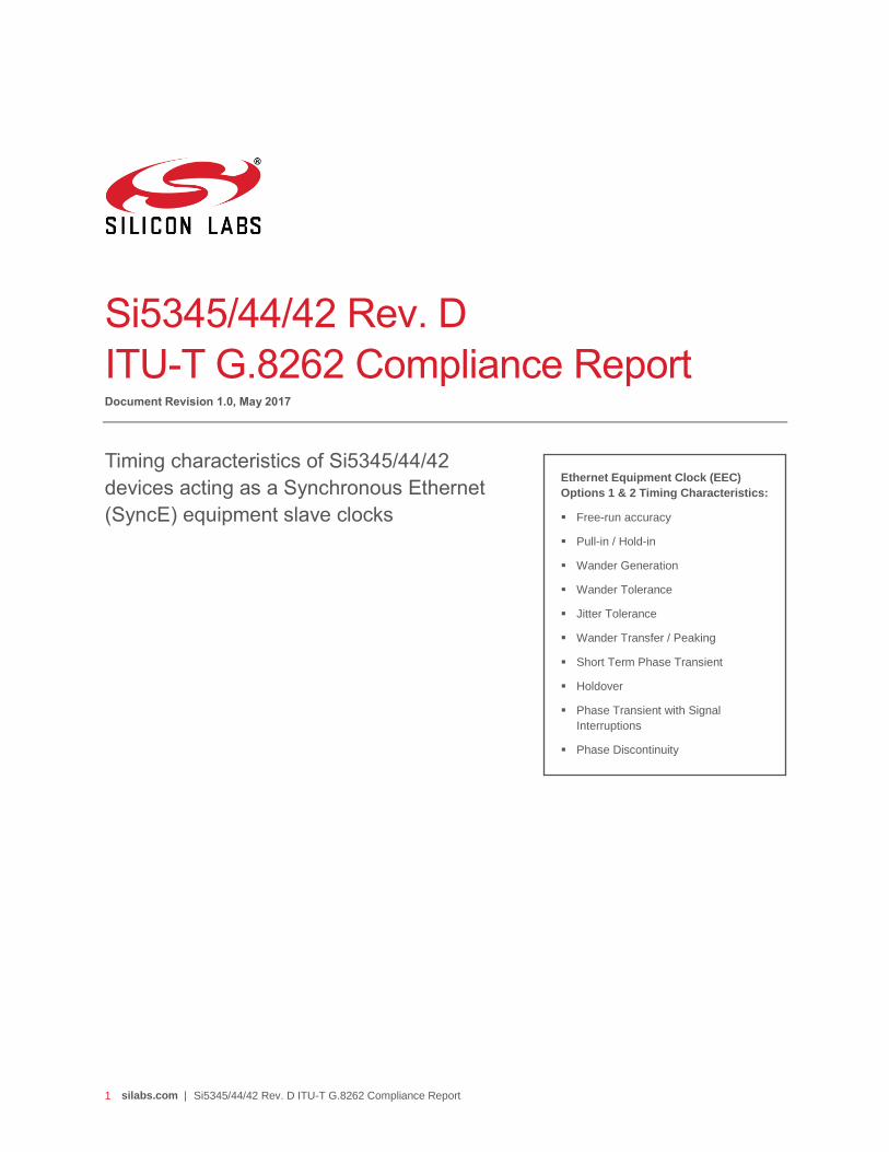
Si5345/44/42 Rev. D
ITU-T G.8262 Compliance Report Document Revision 1.0, May 2017
Timing characteristics of Si5345/44/42
devices acting as a Synchronous Ethernet
(SyncE) equipment slave clocks
Ethernet Equipment Clock (EEC)
Options 1 & 2 Timing Characteristics:
Free-run accuracy
Pull-in / Hold-in
Wander Generation
Wander Tolerance
Jitter Tolerance
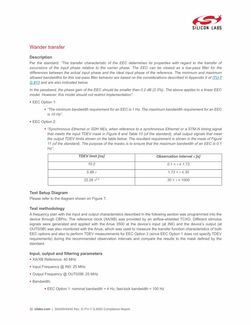
Wander Transfer / Peaking
Short Term Phase Transient
Holdover
Phase Transient with Signal
Interruptions
Phase Discontinuity

2 silabs.com | Si5345/44/42 Rev. D ITU-T G.8262 Compliance Report
Contents
Introduction .................................................................................................................................................................... 3
ITU-T G.8262 Standards Matrix – Compliance Results Summary ................................................................................. 4
Equipment & hardware used during testing ................................................................................................................... 5
Considerations on the use of TCXOs and OCXOs as reference clocks ......................................................................... 6
Measurement considerations ......................................................................................................................................... 6
Setup diagrams color coding .......................................................................................................................................... 6
ClockBuilder Pro frequency plan files ............................................................................................................................. 6
Timing Characteristics .................................................................................................................................................... 7
Free-run accuracy ......................................................................................................................................................................... 7 Pull-in / Hold-in ............................................................................................................................................................................ 10 Wander generation ...................................................................................................................................................................... 14 Wander tolerance ........................................................................................................................................................................ 18 Jitter tolerance ............................................................................................................................................................................. 24 Wander transfer ........................................................................................................................................................................... 32 Short term phase transient .......................................................................................................................................................... 36 Holdover ...................................................................................................................................................................................... 40 Phase transient with signal interruptions ...................................................................................................................................... 44 Phase Discontinuity ..................................................................................................................................................................... 47
Note on jitter generation ............................................................................................................................................... 51
3 silabs.com | Si5345/44/42 Rev. D ITU-T G.8262 Compliance Report
Introduction1
Historically, wide area networks (WANs) have been dominated by synchronous networks based on time division
multiplexing technology, such as SONET/SDH. In order for these networks to transmit and receive data reliably it is
necessary for each element in the network to operate from a local clock frequency that is synchronized to the same
frequency source. Applications such as circuit switched services and wireless backhauls, which operate on these
synchronized networks, depend on very precise timing sources for cases such a call-handoff between two cells.
Such clock sources have been classified according to their accuracy level in stratum levels. A network element (NE) in
a synchronous network has a Stratum 3 local clock with a +/-4.6 ppm free-run frequency accuracy which is synchronized
to a Stratum 2 clock with a +/- 0.016 ppm accuracy, typically referred to as the building integrated timing supply (BITS).
The BITS clock is in turn synchronized to a Stratum 1 clock with a +/- 0.00001 ppm accuracy, otherwise referred to as
an atomic clock. As it can be inferred, due to this synchronization chain, it is necessary for remote network elements to
have a BITS source, in turn traceable to an atomic clock.
Evidently, this is an expensive proposition, so a new model of timing distribution called line timing was adopted. Under
this model, a receiving NE that has recovered a clock from a transmitting NE synchronized to a Stratum 1 clock can re-
transmit the clock to the next NE, thus still ensuring Stratum 1 traceability downstream.
As Ethernet has vastly proliferated over the last few years it has become the preferred data transport mechanism, not
only because of its universal adoption but also because of the lower costs associated with it. However, one limitation
with Ethernet networks is that they are packet-based and as such operate asynchronously. Therefore, they cannot
interoperate with synchronous networks.
The International Telecommunication Union (ITU) has identified two possible solutions for this issue and allow for the
distribution of frequency synchronization through packet networks. One solution is Synchronous Ethernet (SyncE),
which relies on the concept of line timing described above; the second solution is based on Precision Time Protocol
(PTP) under IEEE 1588, which is outside the scope of this document. Under the SyncE model, the free-running local
clocks of the NEs can be replaced with phase-locked loops (PLLs), which are then used to receive and re-transmit a
Stratum 1 traceable clock down the network chain.
ITU’s standard ITU-T G.8262 [Timing characteristics of a synchronous Ethernet equipment slave clock] defines the
performance of PLLs to be used in two different types of Ethernet Equipment Clocks (EECs): EEC Option 1, which is
based on a 2048 kbps rate and is used in Europe and Asia, and EEC Option 2, which is based on a 1544 kbps and is
used in North America.
Silicon Labs’ Si5345/44/42 family of jitter attenuator clock synthesizers are SyncE compliant and as such represent an ideal solution for the implementation of SyncE NEs. They can accept TDM or Ethernet recovered clock frequencies and generate Ethernet clock frequencies that easily meet the jitter performance of 10/40 Gigabit Ethernet PHYs with significant margin. This document presents the results of testing criteria performed on Si5345/44/42 devices, and it shows that they are fully compliant with the SyncE timing characteristics defined by the G.8262 standard, hence qualifying them as EECs.
1 For a more detailed description of several of the concepts introduced in the preceding paragraphs, including graphical representations, please refer to Silicon Labs’ application note AN420 [SyncE and 1588: Sync distribution for a unified network].

4 silabs.com | Si5345/44/42 Rev. D ITU-T G.8262 Compliance Report
ITU-T G.8262 Standards Matrix – Compliance Results Summary
The following table summarizes the timing characteristics tested on SI5345/44/42 devices, along with the corresponding
references to each of the EEC Option standards and the results of each test.
Timing Characteristic EEC Standard Section Compliance Result
Free-run accuracy Option 1
Option 2
G.8262 - 6.1
G.8262 - 6.2
Passed
Passed
Pull-in / Hold-in Option 1
Option 2
G.8262 - 7.1.1
G.8262 - 7.1.2
Passed
Passed
Wander Generation Option 1
Option 2
G.8262 - 8.1.1
G.8262 - 8.1.2
Passed
Passed
Wander Tolerance Option 1
Option 2
G.8262 - 9.1.1
G.8262 - 9.1.2
Passed
Passed
Jitter Tolerance Options 1 & 2 G.8262 - 9.2.1 Passed
Wander Transfer - Peaking Option 1
Option 2
G.8262 - 10.1
G.8262 - 10.2
Passed
Passed
Wander Transfer Option 1
Option 2
Not Applicable
G.8262 - 10.2
Not Applicable
Passed
Shor Term Phase Transient Option 1
Option 2
G.8262 - 11.1.1
G.8262 - 11.1.2
Passed
Passed
Holdover Option 1
Option 2
G.8262 - 11.2.1
G.8262 - 11.2.2
Passed
Passed
Phase Transient with
Signal Interruptions
Option 1
Option 2
G.8262 - 11.3.1
Not Applicable
Passed
Not Applicable
Phase Discontinuity Option 1
Option 2
G.8262 - 11.4.1
G.8262 - 11.4.2
Passed
Passed
5 silabs.com | Si5345/44/42 Rev. D ITU-T G.8262 Compliance Report
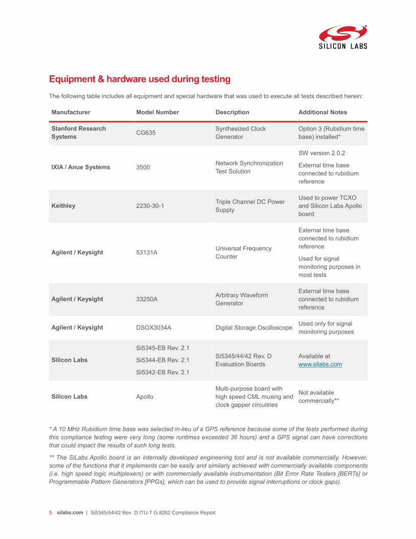
Equipment & hardware used during testing
The following table includes all equipment and special hardware that was used to execute all tests described herein:
Manufacturer Model Number Description Additional Notes
Stanford Research
Systems CG635
Synthesized Clock
Generator
Option 3 (Rubidium time
base) installed*
IXIA / Anue Systems 3500 Network Synchronization
Test Solution
SW version 2.0.2
External time base
connected to rubidium
reference
Keithley 2230-30-1 Triple Channel DC Power
Supply
Used to power TCXO
and Silicon Labs Apollo
board
Agilent / Keysight 53131A Universal Frequency
Counter
External time base
connected to rubidium
reference
Used for signal
monitoring purposes in
most tests
Agilent / Keysight 33250A Arbitrary Waveform
Generator
External time base
connected to rubidium
reference
Agilent / Keysight DSOX3034A Digital Storage Oscilloscope Used only for signal
monitoring purposes
Silicon Labs
Si5345-EB Rev. 2.1
Si5344-EB Rev. 2.1
Si5342-EB Rev. 2.1
Si5345/44/42 Rev. D
Evaluation Boards
Available at
www.silabs.com
Silicon Labs Apollo
Multi-purpose board with
high speed CML muxing and
clock gapper circuitries
Not available
commercially**
* A 10 MHz Rubidium time base was selected in-lieu of a GPS reference because some of the tests performed during
this compliance testing were very long (some runtimes exceeded 36 hours) and a GPS signal can have corrections
that could impact the results of such long tests.
** The SiLabs Apollo board is an internally developed engineering tool and is not available commercially. However,
some of the functions that it implements can be easily and similarly achieved with commercially available components
(i.e. high speed logic multiplexers) or with commercially available instrumentation (Bit Error Rate Testers [BERTs] or
Programmable Pattern Generators [PPGs], which can be used to provide signal interruptions or clock gaps).

6 silabs.com | Si5345/44/42 Rev. D ITU-T G.8262 Compliance Report
Considerations on the use of TCXOs and OCXOs as reference clocks
In order to achieve better wander performance and relative temperature change immunity during scenarios like holdover
it is necessary to use a more stable frequency reference source than just a regular quartz crystal. Temperature
compensated crystal oscillators (TCXOs) and oven compensated crystal oscillators (OCXOs) provide such improved
performance (at a higher price point).
The Si5345/44/42 family of devices can achieve industry leading low phase noise performance and improved
temperature stability when the oscillator used as the external reference has been properly optimized across parameters
such as frequency, Q factor, proper termination, etc.
Silicon Labs’ application note AN905 [Si534x External references; optimizing performance] provides a set of detailed
guidelines that should be followed in order to extract the best performance from any external reference being used.
Such guidelines were followed when performing the testing described herein. It is important to note that a 40 MHz
Rakon RTX Series 513872 TCXO was used as an external reference for all testing described herein.
Measurement considerations
The G.8262 standard specifies the following considerations when performing MTIE and TDEV measurements:
Filtering: use of a 10-Hz, first order, low-pass filter.
An exception should be applied when performing MTIE measurements for EEC Option 2 under transient
response and holdover performance, in which case the recommended cut-off frequency of the filter is 100
Hz.
Sampling time: a maximum rate of 1/30s.
TDEV minimum measurement period: twelve times the integration period.
All of these considerations were followed when performing the testing described herein.
Setup diagrams color coding
The following conventions of colors were used throughout this document to indicate connections on the different test
setups:
Grey wires indicate reference (REF) connections into XA/XB.
Red wires indicate 10 MHz Rubidium time-base distribution.
Green wires indicate connections to PC.
Orange wires indicate connections to the inputs of the device.
Purple wires indicate connections from the outputs of the device.
ClockBuilder Pro frequency plan files
All CBPro frequency plan configuration files used for the testing described herein can be obtained at www.silabs.com.
Note that CBPro version 2.13.2 was used during testing (newer versions of CBPro are constantly published; when
upgrading files to a newer version CBPro automatically reports any potential changes).

7 silabs.com | Si5345/44/42 Rev. D ITU-T G.8262 Compliance Report
Timing Characteristics
Free-run accuracy
Description
Per the standard:
EEC Option 1: “under free-running conditions, the EEC output frequency accuracy should not be greater than 4.6
ppm with regard to a reference traceable to a clock”.
EEC Option 2: “under prolonged holdover conditions, the output frequency accuracy of the different types of node
clocks should not exceed 4.6 ppm with regard to a reference traceable to a primary reference clock”.
Test Setup Diagram
Figure 1: test setup used for free-run measurements
Test methodology
A frequency plan with the input and output characteristics described in the following section was programmed into the
device through ClockBuilder Pro (CBPro). The reference clock (XA/XB) was provided by an airflow-shielded TCXO. No
input clock was provided to the device, hence forcing it to remain in free-run mode. Then the output frequency was
measured with the frequency counter (using a resolution of 1 Hz) every 4 seconds for a few hours and the ppm offset
relative to the reference clock was plotted.
Input, output and filtering parameters
XA/XB Reference: 40 MHz, traceable to Rubidium source
Input Frequency @ IN0: no signal to allow device to free-run
Output Frequency @ OUT0/0B: 40 MHz
Bandwidth:
EEC Option 1: nominal bandwidth = 4 Hz; fast-lock bandwidth = 100 Hz
EEC Option 2: nominal bandwidth = 0.1 Hz; fast-lock bandwidth = 10 Hz
Clock Builder Pro frequency plan files
Si5345-WanderGeneration_Option1.slabtimeproj
Si5345-WanderGeneration_Option2.slabtimeproj
Si534x-EB Rev 2.1
IN0 XB XA
IN1 . .
OUT0 OUT0B
IN2 IN3 53131A Counter
PC
25MHz
10MHz
Q Q* CMOS REFOUT
[BACK]
USB SR CG635
CH1 CH2
10MHz
Supply TCXO

8 silabs.com | Si5345/44/42 Rev. D ITU-T G.8262 Compliance Report
Si5344-WanderGeneration_Option1.slabtimeproj
Si5344-WanderGeneration_Option2.slabtimeproj
Si5342-WanderGeneration_Option1.slabtimeproj
Si5342-WanderGeneration_Option2.slabtimeproj
EEC Option 1 Result: Passed
As it can be seen from the plot shown below, the output frequency remained within +/- 4.6 ppm with respect to the
Rubidium reference for the entire duration of the test while the device was in free-run mode. The blue trace shows the
measured results, which remained between 4.1 and 4.125 ppm. It is important to note that the overall offset corresponds
to the offset of the TCXO relative to the Rubidium reference, and that the TCXO used for this test had been submitted
to accelerated aging. This was done to show that even under those conditions the output frequency remained within
the limits established by the standard.
Figure 2: EEC Option 1 free-run accuracy test result

9 silabs.com | Si5345/44/42 Rev. D ITU-T G.8262 Compliance Report
EEC Option 2 Result: Passed
As it can be seen from the plot shown below, the output frequency remained within +/- 4.6 ppm with respect to the
Rubidium reference for the entire duration of the test while the device was in free-run mode. The blue trace shows the
measured results, which remained between 4.1 and 4.125 ppm. It is important to note that the overall offset corresponds
to the offset of the TCXO relative to the Rubidium reference, and that the TCXO used for this test had been submitted
to accelerated aging. This was done to show that even under those conditions the output frequency remained within
the limits established by the standard.
Figure 3: EEC Option 2 free-run accuracy test result

10 silabs.com | Si5345/44/42 Rev. D ITU-T G.8262 Compliance Report
Pull-in / Hold-in
Description
Per the standard, for both EEC Options: “the minimum pull-in range should be +/- 4.6 ppm, whatever the internal
oscillator frequency offset may be”.
Test Setup Diagram
Figure 4: test setup used for pull-in measurements
Test methodology
A frequency plan with the input and output characteristics described in the following section was programmed into the
device through CBPro. The reference clock (XA/XB) was generated with the clock generator (traceable to the Rubidium
time base) whereas the input clock was generated with the AWG (also traceable to the Rubidium time base) and this
clock was multiplexed using SiLabs Apollo board. The output of the mux was connected to the device’s input (IN1) and
also to the oscilloscope for observation purposes. The device’s output (OUT0/0B) was monitored with the frequency
counter.
Through automation performed with VisualStudio and GPIB instrument control a loop was implemented where first the
reference clock was set to a +4.6 ppm offset and the input clock set to a -4.6 ppm offset from the ideal 40 MHz reference,
respectively. Initially the input clock was disabled (through the mux) so that the part would be free-running. The
frequency counter was triggered to start measuring and 2-3 seconds later the input clock was enabled (through the
mux), taking the device out of free-run state and pulling-in the frequency offset until lock was achieved. The procedure
was repeated with the opposite offsets (-4.6 and 4.6 ppm respectively for the reference and input clocks). The resulting
output frequency measurements were plotted.
Input, output and filtering parameters
XA/XB Reference: 40 MHz
Input Frequency @ IN1: 40 MHz
Output Frequency @ OUT0/0B: 40 MHz
Si534x-EB Rev 2.1
IN0 XB XA
IN1 . .
OUT0 OUT0B
IN2 IN3 53131A Counter
PC
25MHz
10MHz
Q Q* CMOS REFOUT
[BACK]
USB SR CG635
CH1 CH2
10MHz
33250A AWG
OUT
10MHz
40MHz +/- 4.6ppm
40MHz +/- 4.6ppm
Silicon Labs
Gapper Board
Mux IN1
Mux IN2
Mux OUT
CH1 CH2 CH3 CH4
Oscilloscope
BNC Ports: 1 – 10 MHz Reference
2 – Wander Generator
3 – Wander Measurer 1
4 – Wander Measurer 2

11 silabs.com | Si5345/44/42 Rev. D ITU-T G.8262 Compliance Report
Bandwidth:
EEC Option 1: nominal bandwidth = 4 Hz; fast-lock bandwidth disabled
EEC Option 2: nominal bandwidth = 0.1 Hz; fast-lock bandwidth = 1 Hz
Clock Builder Pro frequency plan files
Si5345-PullIn_Option1.slabtimeproj
Si5345-PullIn_Option2.slabtimeproj
Si5344-PullIn_Option1.slabtimeproj
Si5344-PullIn_Option2.slabtimeproj
Si5342-PullIn_Option1.slabtimeproj
Si5342-PullIn_Option2.slabtimeproj

12 silabs.com | Si5345/44/42 Rev. D ITU-T G.8262 Compliance Report
EEC Option 1 Result: Passed
The plot below shows the results of the two cases tested (i.e. opposite offsets at the reference and the input of +4.6
and -4.6 ppm or vice versa). The blue traces correspond to the measured frequency offset (Y axis) across readings in
time (X axis). Readings were performed as fast as the frequency counter was capable of measuring with a resolution
of 1 Hz (i.e. roughly 1 reading per second). The grey dotted traces show the status of the HOFRB alarm, which
corresponds to the Holdover/Freerun register. The purple dotted traces show the status of the LOLB alarm, which
serves as the lock indicator. These two variables are plotted against a secondary Y axis on the right. When HOFRB =
1 the part is in Holdover/Freerun state. It can be seen that as soon as HOFRB toggles to 0 the device starts the locking
process, pulling in the frequencies to achieve a total pull of 9.2 ppm in both cases until the device declares lock (LOLB
= 0).
It can be seen that, due to the 4 Hz of nominal bandwidth programmed on the device, a full pull of 9.2 ppm is achieved
in roughly 13 seconds after the device starts pulling in.
Figure 5: EEC Option 1 pull-in / hold-in test result

13 silabs.com | Si5345/44/42 Rev. D ITU-T G.8262 Compliance Report
EEC Option 2 Results: Passed
The plot below shows the results of the two cases tested (i.e. opposite offsets at the reference and the input of +4.6
and -4.6 ppm or vice versa). The blue traces correspond to the measured frequency offset (Y axis) across readings in
time (X axis). Readings were performed as fast as the frequency counter was capable of measuring with a resolution
of 1 Hz (i.e. roughly 1 reading per second). The grey dotted traces show the status of the HOFRB alarm, which
corresponds to the Holdover/Freerun register. The purple dotted traces show the status of the LOLB alarm, which
serves as the lock indicator. These two variables are plotted against a secondary Y axis on the right. When HOFRB =
1 the part is in Holdover/Freerun state. It can be seen that as soon as HOFRB toggles to 0 the device starts the locking
process, pulling in the frequencies to achieve a total pull of 9.2 ppm in both cases until the device declares lock (LOLB
= 0).
It can be seen that, due to the 0.1 Hz of nominal bandwidth (with a fast lock bandwidth of 1 Hz) programmed on the
device, a full pull of 9.2 ppm is achieved in roughly 38 seconds after the device starts pulling in.
Figure 6: EEC Option 2 pull-in / hold-in test result
14 silabs.com | Si5345/44/42 Rev. D ITU-T G.8262 Compliance Report
Wander generation
Description
Per the standard: “The noise generation of an EEC represents the amount of phase noise produced at the output when
there is an ideal input reference signal or the clock is in holdover state. A suitable reference, for practical testing
purposes, implies a performance level at least 10 times more stable than the output requirements. The ability of the
clock to limit this noise is described by its frequency stability. The measures maximum time interval error (MTIE) and
time deviation (TDEV) are useful for the characterization of noise generation performance”.
EEC Option 1:
MTIE: “When the EEC is in the locked mode of operation synchronized to a wander-free reference, the MTIE
measured using the synchronized clock configuration defined in Figure 1a of ITU-T G.810 should have the
limits shown on the table below, if the temperature is constant (within ±1 °K)”.
MTIE limit [ns] Observation interval [s]
40 0.1 < ≤ 1
40 0.1 1 < ≤ 100
25.25 0.2 100 < ≤ 1000
TDEV: “When the EEC is in the locked mode of operation, the TDEV measured using the synchronized clock
configuration defined in Figure 1a of ITU-T G.810 should have the limits shown on the table below, if the
temperature is constant (within ±1 °K)”.
TDEV limit [ns] Observation interval [s]
3.2 0.1 < ≤ 25
0.64 0.5 25 < ≤ 100
6.4 100 < ≤ 1000
EEC Option 2:
MTIE: “When the EEC is in the locked mode of operation synchronized to a wander-free reference, the MTIE
measured using the synchronized clock configuration defined in Figure 1a of ITU-T G.810 should have the
limits shown on the table below, if the temperature is constant (within ±1 °K)”.
MTIE limit [ns] Observation interval [s]
20 0.1 < ≤ 1
20 0.48 1 < ≤ 10
60 10 < ≤ 1000
TDEV: “When the EEC is in the locked mode of operation, the TDEV measured using the synchronized clock
configuration defined in Figure 1a of ITU-T G.810 should have the limits shown on the table below, if the
temperature is constant (within ±1 °K)”.

15 silabs.com | Si5345/44/42 Rev. D ITU-T G.8262 Compliance Report
TDEV limit [ns] Observation interval [s]
3.2 -0.5 0.1 < ≤ 25
2 2.5 < ≤ 40
0.32 0.5 40 < ≤ 1000
10 1000 < ≤ 10000
Test Setup Diagram
Figure 7: test setup used for wander generation / tolerance / transfer and holdover measurements
Test methodology
A frequency plan with the input and output characteristics described in the following section was programmed into the
device through CBPro. The reference clock (XA/XB) was provided by an airflow-shielded TCXO. A 25 MHz input was
generated with the Anue 3500 (at IN0) and the device’s output (at OUT0/0B) was also monitored with the Anue, which
was used to perform MTIE and TDEV measurements during the recommended observation intervals and compare the
results to the masks also defined by the standards.
Input, output and filtering parameters
XA/XB Reference: 40 MHz
Input Frequency @ IN0: 25 MHz
Output Frequency @ OUT0/0B: 25 MHz
Bandwidth:
EEC Option 1: nominal bandwidth = 4 Hz; fast-lock bandwidth = 100 Hz
EEC Option 2: nominal bandwidth = 0.1 Hz; fast-lock bandwidth = 10 Hz
TCXO
Si534x-EB Rev 2.1
IN0
ANUE 3500
25MHz
XB XA
2 4
1 3 S
S
BNC Connect
IN1 . .
OUT0 OUT0B
IN2 IN3 53131A Counter
Management
PC
100 MHz/4 = 25MHz
25MHz
10MHz
Q Q* CMOS REFOUT
[BACK]
USB
Supply
SR CG635
CH1 CH2
10MHz
BNC Ports: 1 – 10 MHz Reference
2 – Wander Generator
3 – Wander Measurer 1
4 – Wander Measurer 2

16 silabs.com | Si5345/44/42 Rev. D ITU-T G.8262 Compliance Report
Clock Builder Pro frequency plan files
Si5345-WanderGeneration_Option1.slabtimeproj
Si5345-WanderGeneration_Option2.slabtimeproj
Si5344-WanderGeneration_Option1.slabtimeproj
Si5344-WanderGeneration_Option2.slabtimeproj
Si5342-WanderGeneration_Option1.slabtimeproj
Si5342-WanderGeneration_Option2.slabtimeproj
EEC Option 1 Results: Passed
As it can be seen on the plot shown below, the measured MTIE (solid green line) and TDEV (solid blue line) results
were below the MTIE and TDEV masks (dashed green and blue lines, respectively) defined by the standards.
Figure 8: EEC Option 1 wander generation test result

17 silabs.com | Si5345/44/42 Rev. D ITU-T G.8262 Compliance Report
EEC Option 2 Results: Passed
As it can be seen on the plot shown below, the measured MTIE (solid green line) and TDEV (solid blue line) results
were below the MTIE and TDEV masks (dashed green and blue lines, respectively) defined by the standards.
Figure 9: EEC Option 2 wander generation test result

18 silabs.com | Si5345/44/42 Rev. D ITU-T G.8262 Compliance Report
Wander tolerance
Description
Per the standard:
“The noise tolerance of an EEC indicates the minimum phase noise level at the input of the clock that should be
accommodated whilst:
- maintaining the clock within prescribed performance limits. The exact performance limits are for further study;
- not causing any alarms;
- not causing the clock to switch reference;
- not causing the clock to go into holdover.”
Test Setup Diagram
Please refer to the diagram shown on Figure 7.
Test methodology
A frequency plan with the input and output characteristics described in the following section was programmed into the
device through CBPro. The reference clock (XA/XB) was provided by an airflow-shielded TCXO. Different stimulus
signals (as described below) were generated and applied with the Anue 3500 at the device’s input (at IN0). Using
CBPro’s Evaluation Board (EVB) GUI the device’s main alarms were monitored prior, during and after the stimulus to
verify the device’s wander tolerance capability.
Per the standard “The TDEV signal used for a conformance test should be generated by adding white, Gaussian noise
sources, of which each has been filtered to obtain the proper type of noise process with the proper amplitude”. As
illustrated on the next two images, the generated stimuli (shown in the dark blue line) follow closely the standard
recommendation (dashed blue line).
Figure 10: EEC Option 1 wander tolerance stimulus TDEV

19 silabs.com | Si5345/44/42 Rev. D ITU-T G.8262 Compliance Report
Figure 11: EEC Option 2 wander tolerance stimulus TDEV
Input, output and filtering parameters
XA/XB Reference: 40 MHz
Input Frequency @ IN0: 25 MHz
Output Frequency @ OUT0/0B: 25 MHz
Bandwidth:
EEC Option 1: nominal bandwidth = 4 Hz; fast-lock bandwidth = 100 Hz
EEC Option 2: nominal bandwidth = 0.1 Hz; fast-lock bandwidth = 10 Hz
Clock Builder Pro frequency plan files
The same CBPro files that were used for wander generation apply to this section as well.
EEC Option 1 Results: Passed
The images below show an overlay of the CBPro EVB GUI illustrating the status of the device’s alarms at the beginning
and end of the test (note that the “Sticky” alarms are the most important here since they show that alarms were never
set during the duration of the test). The side-inserts also illustrate the concurrent start and end of the stimulus application
from the Anue “TIE playback” feature. Timestamps of the alarm monitoring readings can also be corroborated on the
images (at the bottom).
Note that:
a) These tests had a long duration and as such some of the timestamps can roll into the next day.
b) When an alarm is “clear” the corresponding alarm indicator should have a “white” status. When an alarm is
“set” the corresponding alarm indicator should have a “red” status.
c) Registers and alarms not relevant to the test were greyed out on the images to avoid confusion.

20 silabs.com | Si5345/44/42 Rev. D ITU-T G.8262 Compliance Report
Figure 12: EEC Option 1 wander tolerance - device alarms prior to test

21 silabs.com | Si5345/44/42 Rev. D ITU-T G.8262 Compliance Report
Figure 13: EEC Option 1 wander tolerance - device alarms after test
22 silabs.com | Si5345/44/42 Rev. D ITU-T G.8262 Compliance Report
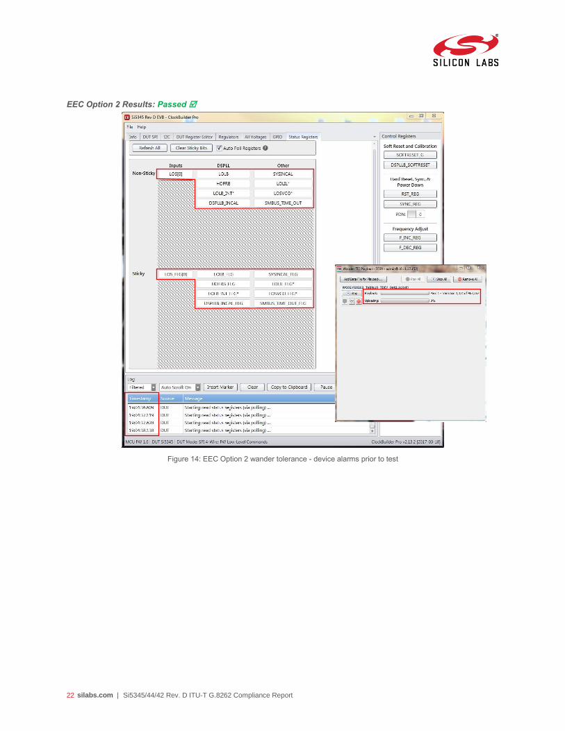
EEC Option 2 Results: Passed
Figure 14: EEC Option 2 wander tolerance - device alarms prior to test

23 silabs.com | Si5345/44/42 Rev. D ITU-T G.8262 Compliance Report
Figure 15: EEC Option 2 wander tolerance - device alarms after test
24 silabs.com | Si5345/44/42 Rev. D ITU-T G.8262 Compliance Report
Jitter tolerance
Description
Per the standard:
EEC Options 1 & 2:
1G: “The lower limit of maximum tolerable input jitter for 1G Ethernet interfaces is given by the table below”.
Peak-peak jitter amplitude (UI) Frequency f (Hz)
312.5 10 < f ≤ 12.1
3750 f-1 12.1 < f ≤ 2.5 k
1.5 2.5 k < f ≤ 50 k
10G: “The lower limit of maximum tolerable input jitter for 10G Ethernet interfaces is given by the table
below”.
Peak-peak jitter amplitude (UI) Frequency f (Hz)
2488 10 < f ≤ 12.1
30000 f-1 12.1 < f ≤ 20 k
1.5 20 k < f ≤ 40 k
Test Setup Diagram
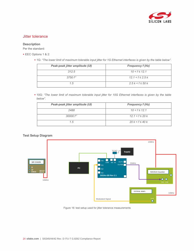
Figure 16: test setup used for jitter tolerance measurements
Si534x-EB Rev 2.1
IN0 XB XA
TCXO
IN1 . .
OUT0 OUT0B
IN2 IN3 53131A Counter
PC
25MHz
10MHz
Q Q* CMOS REFOUT
[BACK]
USB
Supply
SR CG635
CH1 CH2
10MHz
33250A AWG
OUT
10MHz
Modulated Signal

25 silabs.com | Si5345/44/42 Rev. D ITU-T G.8262 Compliance Report
Test methodology
A frequency plan with the input and output characteristics described in the following section was programmed into the
device through CBPro. The reference clock (XA/XB) was provided by an airflow-shielded TCXO. A 25 MHz frequency
modulated signal was generated with the AWG in order to provide an input clock at IN1.
For each of the modulation frequencies proposed by the standard a modulation deviation sweep was performed using
automation until either the physical capabilities of the AWG were reached or until one of the device’s alarms was set
(i.e. until a “breaking point” was found). The results were then plotted along the standard’s proposed masks.
Input, output and filtering parameters
XA/XB Reference: 40 MHz
Input Frequency @ IN1: 25 MHz
Output Frequency @ OUT0/0B: 25 MHz
Bandwidth:
EEC Option 1: nominal bandwidth = 4 Hz; fast-lock bandwidth = 100 Hz
EEC Option 2: nominal bandwidth = 0.1 Hz; fast-lock bandwidth = 10 Hz
Clock Builder Pro frequency plan files
Si5345_JitterTolerance_Option1.slabtimeproj
Si5345_JitterTolerance_Option2.slabtimeproj
Si5344_JitterTolerance_Option1.slabtimeproj
Si5344_JitterTolerance_Option2.slabtimeproj
Si5342_JitterTolerance_Option1.slabtimeproj
Si5342_JitterTolerance_Option2.slabtimeproj
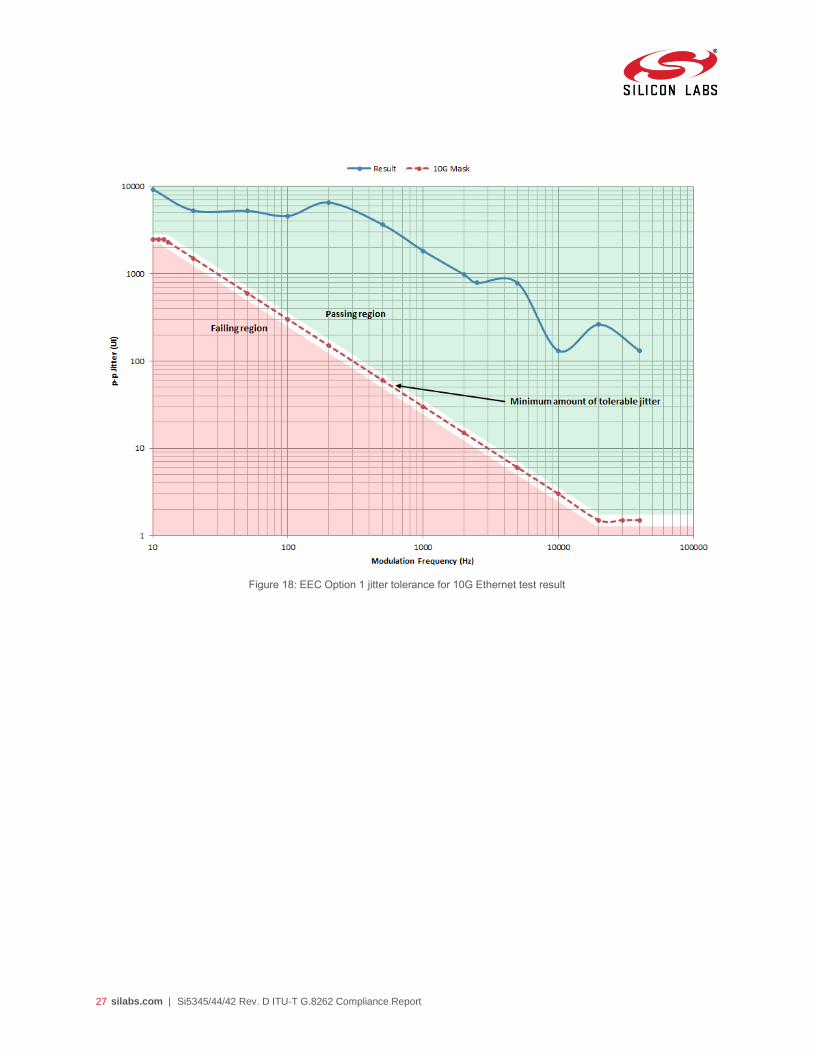
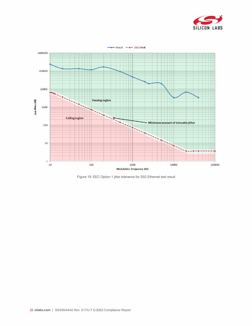
EEC Option 1 Results: Passed
The images below show the jitter tolerance of the device for 1G, 10G and 25G synchronous Ethernet. The mask defined
by the standard is shown on the red dashed line, whereas the result is shown on the blue solid line. Note that in this
case the results are expected to be above the mask (the mask defines a minimum amount of jitter to be tolerated), so
shaded red and green sections were added to the plot to facilitate the interpretation of the results.

26 silabs.com | Si5345/44/42 Rev. D ITU-T G.8262 Compliance Report
Figure 17: EEC Option 1 jitter tolerance for 1G Ethernet test result
27 silabs.com | Si5345/44/42 Rev. D ITU-T G.8262 Compliance Report
Figure 18: EEC Option 1 jitter tolerance for 10G Ethernet test result
28 silabs.com | Si5345/44/42 Rev. D ITU-T G.8262 Compliance Report
Figure 19: EEC Option 1 jitter tolerance for 25G Ethernet test result

29 silabs.com | Si5345/44/42 Rev. D ITU-T G.8262 Compliance Report
EEC Option 2 Results: Passed
The images below show the jitter tolerance of the device for 1G, 10G and 25G synchronous Ethernet. The mask defined
by the standard is shown on the red dashed line, whereas the result is shown on the blue solid line. Note that in this
case the results are expected to be above the mask (the mask defines a minimum amount of jitter to be tolerated), so
shaded red and green sections were added to the plot to facilitate the interpretation of the results.
Figure 20: EEC Option 2 jitter tolerance for 1G Ethernet test result

30 silabs.com | Si5345/44/42 Rev. D ITU-T G.8262 Compliance Report
Figure 21: EEC Option 2 jitter tolerance for 10G Ethernet test result

31 silabs.com | Si5345/44/42 Rev. D ITU-T G.8262 Compliance Report
Figure 22: EEC Option 2 jitter tolerance for 25G Ethernet test result
32 silabs.com | Si5345/44/42 Rev. D ITU-T G.8262 Compliance Report
Wander transfer
Description
Per the standard: “The transfer characteristic of the EEC determines its properties with regard to the transfer of
excursions of the input phase relative to the carrier phase. The EEC can be viewed as a low-pass filter for the
differences between the actual input phase and the ideal input phase of the reference. The minimum and maximum
allowed bandwidths for this low-pass filter behavior are based on the considerations described in Appendix II of ITU-T
G.813 and are also indicated below.
In the passband, the phase gain of the EEC should be smaller than 0.2 dB (2.3%). The above applies to a linear EEC
model. However, this model should not restrict implementation”.
EEC Option 1:
“The minimum bandwidth requirement for an EEC is 1 Hz. The maximum bandwidth requirement for an EEC
is 10 Hz”.
EEC Option 2:
“Synchronous Ethernet or SDH NEs, when reference to a synchronous Ethernet or a STM-N timing signal
that meets the input TDEV mask in Figure 8 and Table 10 (of the standard), shall output signals that meet
the output TDEV limits shown on the table below. The resultant requirement is shown in the mask of Figure
11 (of the standard). The purpose of the masks is to ensure that the maximum bandwidth of an EEC is 0.1
Hz”.
TDEV limit [ns] Observation interval [s]
10.2 0.1 < ≤ 1.73
5.88 1.73 < ≤ 30
32.26 0.5 30 < ≤ 1000
Test Setup Diagram
Please refer to the diagram shown on Figure 7.
Test methodology
A frequency plan with the input and output characteristics described in the following section was programmed into the
device through CBPro. The reference clock (XA/XB) was provided by an airflow-shielded TCXO. Different stimulus
signals were generated and applied with the Anue 3500 at the device’s input (at IN0) and the device’s output (at
OUT0/0B) was also monitored with the Anue, which was used to measure the transfer function characteristics of both
EEC options and also to perform TDEV measurements for EEC Option 2 (since EEC Option 1 does not specify TDEV
requirements) during the recommended observation intervals and compare the results to the mask defined by the
standard.
Input, output and filtering parameters
XA/XB Reference: 40 MHz
Input Frequency @ IN0: 25 MHz
Output Frequency @ OUT0/0B: 25 MHz
Bandwidth:
EEC Option 1: nominal bandwidth = 4 Hz; fast-lock bandwidth = 100 Hz

33 silabs.com | Si5345/44/42 Rev. D ITU-T G.8262 Compliance Report
EEC Option 2: nominal bandwidth = 0.1 Hz; fast-lock bandwidth = 10 Hz
Clock Builder Pro frequency plan files
The same CBPro files that were used for wander generation apply to this section as well.
EEC Option 1 Results: Passed
The image below shows the transfer function characteristics of the EEC clock. The device’s bandwidth was
programmed at 4 Hz, and as it can be observed, the resulting bandwidth was exactly 4 Hz (@ -3dB), with a maximum
peaking of 0.0383 dB, thus also satisfying the peaking limit of 0.2 dB.
Figure 23: EEC Option 1 wander transfer characteristic test result
-3dB point

34 silabs.com | Si5345/44/42 Rev. D ITU-T G.8262 Compliance Report
EEC Option 2 Results: Passed
The image below shows the transfer function characteristics of the EEC clock. The device’s bandwidth was
programmed at 0.1 Hz, and as it can be observed, the resulting bandwidth was 0.06 Hz (@ -3dB), with a maximum
peaking of 0.0527 dB, thus also satisfying the peaking limit of 0.2 dB.
Figure 24: EEC Option 2 wander transfer characteristic test result
-3dB point

35 silabs.com | Si5345/44/42 Rev. D ITU-T G.8262 Compliance Report
The image below shows the transfer TDEV characteristics of the EEC clock. As it can be observed, the result (solid
blue line) is below the mask defined by the standard (dashed blue line).
Figure 25: EEC Option 2 wander transfer TDEV test result
36 silabs.com | Si5345/44/42 Rev. D ITU-T G.8262 Compliance Report
Short term phase transient
Description
Per the standard: “This requirement reflects the performance of the clock in cases when the (selected) input reference
is lost due to a failure in the reference path and a second reference input signal, traceable to the same reference clock,
is available simultaneously, or shortly after the detection of the failure (e.g. in cases of autonomous restoration). In such
cases the reference is lost for at most 15 seconds. The output phase variation, relative to the input reference before it
was lost, is bounded by the following requirements”.
EEC Option 1:
“The phase error should not exceed t + 5 x 10⁻⁸ x S seconds over any period S up to 15 seconds. t
represents two phase jumps that may occur during the transition into and out of the holdover state which
both should not exceed 120 ns with a temporary frequency offset of no more than 7.5 ppm. In cases where
the input synchronization signal is lost for more than 15 seconds, the requirements for long-term phase
transient response (Holdover) should apply”.
EEC Option 2:
“During clock rearrangement operations (e.g. reference switching), the output of the clock should meet the
MTIE requirements shown below”.
MTIE limit [ns] Observation interval [s]
Not specified ≤ 0.014
7.6 + 885 0.014 < ≤ 0.5
300 + 300 0.5 < ≤ 2.33
1000 2.33 <
Test Setup Diagram
Figure 26: test setup used for short term phase transient measurements
Si534x-EB Rev 2.1
IN0
ANUE 3500
25MHz
XB XA
TCXO
2 4
1 3 S
S
BNC Connect
IN1 . .
OUT0 OUT0B
IN2 IN3 53131A Counter
Management
PC
100 MHz/4 = 25MHz
25MHz
10MHz
Q Q* CMOS REFOUT
[BACK]
USB
Supply
SR CG635
CH1 CH2
10MHz
Silicon Labs
Gapper Board
Mux IN1
Mux IN2
Mux OUT
CH1 CH2 CH3 CH4
Oscilloscope
25MHz
BNC Ports: 1 – 10 MHz Reference
2 – Wander Generator
3 – Wander Measurer 1
4 – Wander Measurer 2
37 silabs.com | Si5345/44/42 Rev. D ITU-T G.8262 Compliance Report
Test methodology
A frequency plan with the input and output characteristics described in the following section was programmed into the
device through CBPro. The reference clock (XA/XB) was provided by an airflow-shielded TCXO. A 25 MHz input was
generated with the Anue 3500 and this clock was multiplexed using SiLabs Apollo board. The output of the mux was
connected to the device’s input (IN0) and also to the oscilloscope for observation purposes. The device’s output (at
OUT0/0B) was monitored with the Anue, which was used to perform MTIE measurements during the recommended
observation intervals and compare the results to the masks also defined by the standards. During the execution of the
test the channel control signal of the mux was manually toggled twice during an interval of 15 seconds in order to
generate two signal interruptions at the device’s input (by selecting a second mux channel with no signal on it).
Input, output and filtering parameters
XA/XB Reference: 40 MHz
Input Frequency @ IN0: 25 MHz
Output Frequency @ OUT0/0B: 25 MHz
Bandwidth:
EEC Option 1: nominal bandwidth = 4 Hz; fast-lock bandwidth = 100 Hz
EEC Option 2: nominal bandwidth = 0.1 Hz; fast-lock bandwidth = 10 Hz
Clock Builder Pro frequency plan files
Si5345_PhaseTransient_ShortHO_Option1.slabtimeproj
Si5345_PhaseTransient_ShortHO_Option2.slabtimeproj
Si5344_PhaseTransient_ShortHO_Option1.slabtimeproj
Si5344_PhaseTransient_ShortHO_Option2.slabtimeproj
Si5342_PhaseTransient_ShortHO_Option1.slabtimeproj
Si5342_PhaseTransient_ShortHO_Option2.slabtimeproj
38 silabs.com | Si5345/44/42 Rev. D ITU-T G.8262 Compliance Report
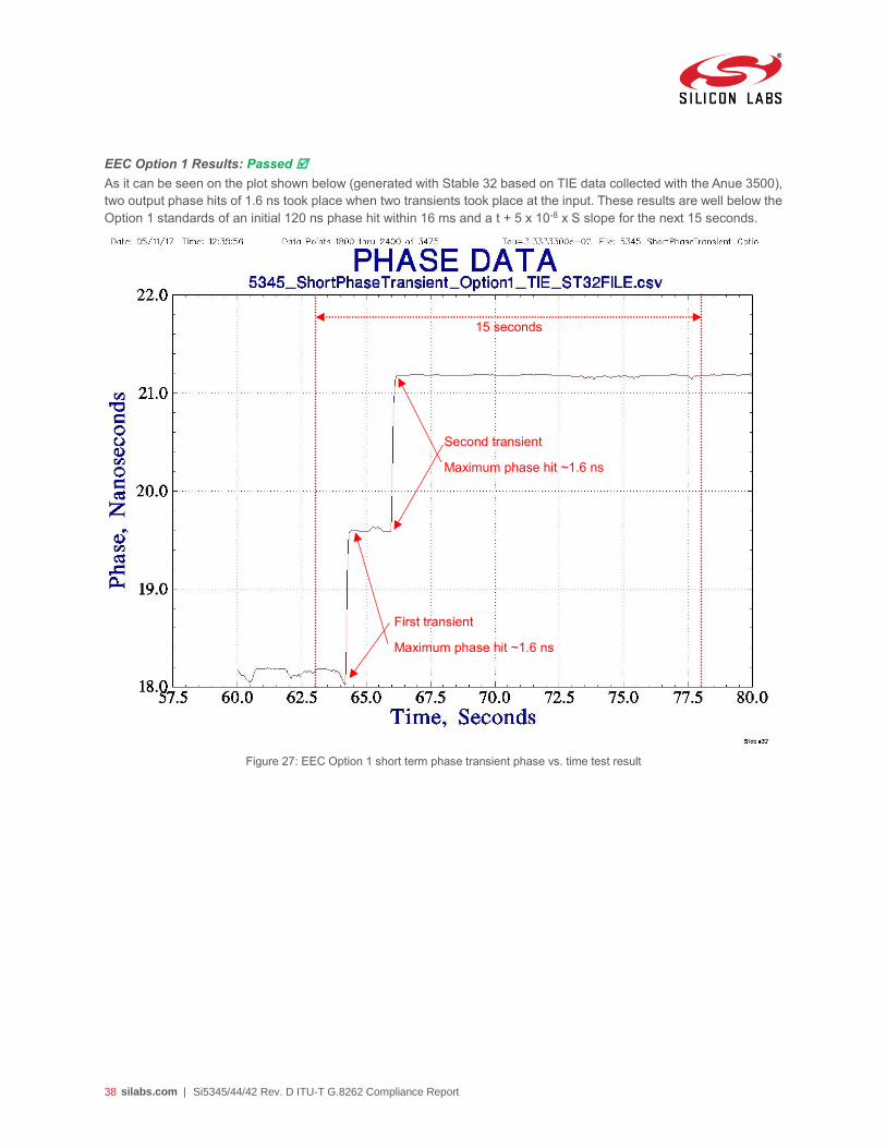
EEC Option 1 Results: Passed
As it can be seen on the plot shown below (generated with Stable 32 based on TIE data collected with the Anue 3500),
two output phase hits of 1.6 ns took place when two transients took place at the input. These results are well below the
Option 1 standards of an initial 120 ns phase hit within 16 ms and a t + 5 x 10⁻⁸ x S slope for the next 15 seconds.
Figure 27: EEC Option 1 short term phase transient phase vs. time test result
15 seconds
First transient
Maximum phase hit ~1.6 ns
Second transient
Maximum phase hit ~1.6 ns

39 silabs.com | Si5345/44/42 Rev. D ITU-T G.8262 Compliance Report
EEC Option 2 Results: Passed
As it can be seen on the plot shown below, the measured MTIE (solid green line) result was below the MTIE mask
(dashed green line) defined by the standard.
Figure 28: EEC Option 2 short term phase transient MTIE test result

40 silabs.com | Si5345/44/42 Rev. D ITU-T G.8262 Compliance Report
Holdover
Description
Per the standard: “This requirement bounds the maximum excursions in the output timing signal. Additionally, it restricts
the accumulation of the phase movement during input signal impairments or internal disturbances”.
EEC Option 1:
“When the EEC loses all its references, it is said to enter the holdover state. The phase error, T, at the
output of the EEC relative to the input at the moment of loss of reference should not, over any period of S >
15 s, exceed the following limit:
∆𝑇(𝑆) = {(𝑎1 + 𝑎2)𝑆 + 0.5𝑏𝑆2 + 𝑐} [𝑛𝑠]
Where:
o a1 = 50 ns/s
o a2 = 2000 ns/s
o b = 1.16 x 10⁻⁴ ns/s2
o c = 120 ns”
EEC Option 2:
“When an EEC clock loses all its references, it enters the holdover state. The phase error, T, at the output
of the slave clock from the moment of loss or reference, should, over any period of S seconds, meet the
following:
|∆𝑇(𝑆)| ≤ {(𝑎1 + 𝑎2)𝑆 + 0.5𝑏𝑆2 + 𝑐} [𝑛𝑠]
The derivative of T(S), the fractional frequency offset, should, over any period of S seconds, meet the
following:
|𝑑(∆𝑇(𝑆))
𝑑𝑆| ≤ {𝑎1 + 𝑎2 + 𝑏𝑆} [
𝑛𝑠
𝑠]
The second derivative of T(S), the fractional frequency drift, should, over any period of S seconds, meet
the following:
|𝑑2(∆𝑇(𝑆))
𝑑𝑆2 | ≤ 𝑑 [𝑛𝑠
𝑠2]
Where:
Applies for S > TBD
a1 [ns/s] 50
a2 [ns/s] 300
b [ns/s2] 4.63 x 10⁻⁴
c [ns] 1000
d [ns/s2] 4.63 x 10⁻⁴
41 silabs.com | Si5345/44/42 Rev. D ITU-T G.8262 Compliance Report
In applying the above requirements for the derivative of T(S) and the second derivative of T(S), the period
S must begin after any transient associated with entre into holdover is over”.
Test Setup Diagram
Please refer to the diagram shown on Figure 7.
Test methodology
A frequency plan with the input and output characteristics described in the following section was programmed into the
device through CBPro. The reference clock (XA/XB) was provided by an airflow-shielded TCXO. A 25 MHz input was
generated with the Anue 3500 (at IN0) and the device’s output (at OUT0/0B) was also monitored with the Anue, which
was used to perform MTIE measurements during the recommended observation intervals and compare the results to
the masks also defined by the standards. At the very beginning of the test the device was locked to the input provided
by the Anue; after a few seconds the device was forced through a register write to switch to another input (IN1), which
had no valid signal, hence forcing the device to go into holdover during the rest of the test.
Input, output and filtering parameters
XA/XB Reference: 40 MHz
Input Frequency @ IN0: 25 MHz
Output Frequency @ OUT0/0B: 25 MHz
Bandwidth:
EEC Option 1: nominal bandwidth = 4 Hz; fast-lock bandwidth = 100 Hz
EEC Option 2: nominal bandwidth = 0.1 Hz; fast-lock bandwidth = 10 Hz
Clock Builder Pro frequency plan files
Si5345_Holdover_Option1.slabtimeproj
Si5345_Holdover_Option2.slabtimeproj
Si5344_Holdover_Option1.slabtimeproj
Si5344_Holdover_Option2.slabtimeproj
Si5342_Holdover_Option1.slabtimeproj
Si5342_Holdover_Option2.slabtimeproj
42 silabs.com | Si5345/44/42 Rev. D ITU-T G.8262 Compliance Report
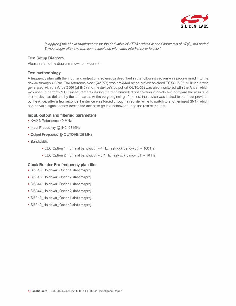
EEC Option 1 Results: Passed
As it can be seen on the plot shown below, the measured MTIE (solid green line) result was below the MTIE mask
(dashed green line) defined by the standard.
Figure 29: EEC Option 1 holdover MTIE test result

43 silabs.com | Si5345/44/42 Rev. D ITU-T G.8262 Compliance Report
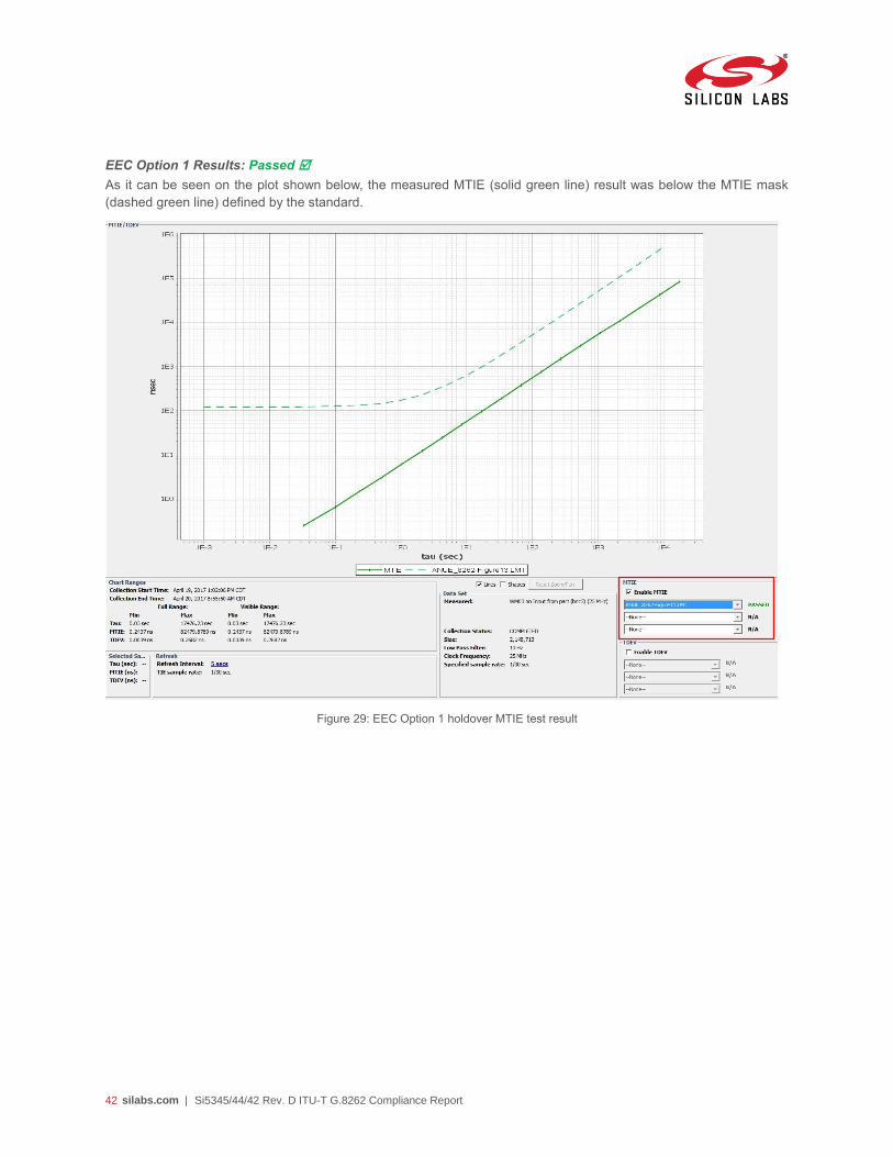
EEC Option 2 Results: Passed
As it can be seen on the plot shown below, the measured MTIE (solid green line) result was below the MTIE mask
(dashed green line) defined by the standard.
Figure 30: EEC Option 2 holdover MTIE test result
44 silabs.com | Si5345/44/42 Rev. D ITU-T G.8262 Compliance Report
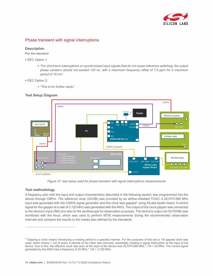
Phase transient with signal interruptions
Description
Per the standard:
EEC Option 1:
“For short-term interruptions on synchronized input signals that do not cause reference switching, the output
phase variation should not exceed 120 ns, with a maximum frequency offset of 7.5 ppm for a maximum
period of 16 ms”.
EEC Option 2:
“This is for further study”.
Test Setup Diagram
Figure 31: test setup used for phase transient with signal interruptions measurements
Test methodology
A frequency plan with the input and output characteristics described in the following section was programmed into the
device through CBPro. The reference clock (XA/XB) was provided by an airflow-shielded TCXO. A 28.5741286 MHz
input was generated with the CG635 signal generator and this clock was gapped2 using SiLabs Apollo board. A control
signal for the gapper at a rate of 3.125 MHz was generated with the AWG. The output of the clock gapper was connected
to the device’s input (IN0) and also to the oscilloscope for observation purposes. The device’s output (at OUT0/0B) was
monitored with the Anue, which was used to perform MTIE measurements during the recommended observation
intervals and compare the results to the masks also defined by the standards.
2 Gapping a clock means introducing a missing period in a graceful manner. For the purposes of this test a 1/8 gapped clock was
used, which means 1 out of every 8 periods of the clock was removed, essentially creating a signal interruption at the input of the device. Due to this, the effective clock rate seen at the input of the device was 28.5741286 MHz * 7/8 = 25 MHz. The control signal generated by the AWG had a frequency of 25 MHz * 1/8 = 3.125 MHz.
Si534x-EB Rev 2.1
IN0
ANUE 3500
25MHz
XB XA
TCXO
2 4
1 3 S
S
BNC Connect
IN1 . .
OUT0 OUT0B
IN2 IN3
53131A Counter
Management
PC
28.5741286MHz
25MHz
10MHz
Q Q* CMOS REFOUT
[BACK]
USB
Supply
SR CG635 CH1 CH2
10MHz
Silicon Labs
Gapper Board
CLK IN
CKLK OUT GAP CMD CLK OUT*
CH1 CH2 CH3 CH4
Oscilloscope
25MHz (Gapped)
33250A AWG
OUT
BNC Ports: 1 – 10 MHz Reference
2 – Wander Generator
3 – Wander Measurer 1
4 – Wander Measurer 2

45 silabs.com | Si5345/44/42 Rev. D ITU-T G.8262 Compliance Report
Input, output and filtering parameters
XA/XB Reference: 40 MHz
Input Frequency @ IN0: 25 MHz
Output Frequency @ OUT0/0B: 25 MHz
Bandwidth:
EEC Option 1: nominal bandwidth = 4 Hz; fast-lock bandwidth = 100 Hz
Clock Builder Pro frequency plan files
Si5345_PhaseTransient_ShortHO_INTERRUPT_Option1.slabtimeproj
Si5344_PhaseTransient_ShortHO_INTERRUPT_Option1.slabtimeproj
Si5342_PhaseTransient_ShortHO_INTERRUPT_Option1.slabtimeproj

46 silabs.com | Si5345/44/42 Rev. D ITU-T G.8262 Compliance Report
EEC Option 1 Results: Passed
As it can be seen on the plot shown below (generated with Stable 32 based on TIE data collected with the Anue 3500),
a phase hit of ~5 ns took place when a signal interruption occurred at the input. These results are well below the Option
1 standards of an initial 120 ns phase hit within 16 ms. Note that in this case the TIE data was collected with a sampling
constant () of 1 ms in order to easily comply with the 16 ms standard limit.
Figure 32: EEC Option 1 phase transient with signal interruptions phase vs. time test result
EEC Option 2 Results: not tested since there is no standard defined for EEC Option 2.
Maximum phase hit ~5 ns

47 silabs.com | Si5345/44/42 Rev. D ITU-T G.8262 Compliance Report
Phase Discontinuity
Description
Per the standard:
EEC Option 1:
“In cases of infrequent internal testing or other internal disturbances (but excluding major hardware failures,
e.g., those that would give rise to clock equipment protection switches) within the synchronous Ethernet
equipment clock, the following conditions should be met:
o The phase variation over any period S (ms) up to 16 ms should not exceed 7.5S ns;
o The phase variation over any period S (ms) from 16 ms up to 2.4 s should not exceed 120 ns;
o For periods greater than 2.4 s, the phase variation for each interval of 2.4 s should not exceed 120
ns with a temporary offset of no more than 7.5 ppm up to a total amount of 1 s”.
EEC Option 2:
“In cases of infrequent internal testing or rearrangement operations within the slave clock, the phase
transient at the output of EEC-Option 2 should meet the MTIE specifications defined on the table below”
MTIE limit [ns] Observation interval [s]
Not specified ≤ 0.014
7.6 + 885 0.014 < ≤ 0.5
300 + 300 0.5 < ≤ 2.33
1000 2.33 <
Test Setup Diagram
Figure 33: test setup used for phase discontinuity measurements
Si534x-EB Rev 2.1
IN0
ANUE 3500
25MHz
XB XA
TCXO
2 4
1 3 S
S
BNC Connect
IN1 . .
OUT0 OUT0B
IN2 IN3 53131A Counter
Management
PC
8kHz 25MHz
10MHz
Q Q* CMOS REFOUT
[BACK]
USB
Supply
SR CG635
CH1 CH2
10MHz
Phase matched cables
BNC Ports: 1 – 10 MHz Reference
2 – Wander Generator
3 – Wander Measurer 1
4 – Wander Measurer 2

48 silabs.com | Si5345/44/42 Rev. D ITU-T G.8262 Compliance Report
Test methodology
A frequency plan with the input and output characteristics described in the following section was programmed into the
device through CBPro. The reference clock (XA/XB) was provided by an airflow-shielded TCXO. An 8 kHz differential
input was generated with the CG635 signal generator and each complimentary leg of the differential pair was connected
to the IN0 and IN1 device inputs, respectively, essentially providing two single-ended 8 kHz input clocks with complete
phase discontinuity (180° apart). The device’s output (at OUT0/0B) was monitored with the Anue, which was used to
perform MTIE measurements during the recommended observation intervals and compare the results to the masks
also defined by the standards. During the execution of the test the device was initially locked to the IN0 clock; then after
a few seconds a manual switch was performed to switch to the IN1 clock (180° apart). After 60 seconds another manual
switch was performed to return to the IN0 clock.
Input, output and filtering parameters
XA/XB Reference: 40 MHz
Input Frequency @ IN0 & IN1: 8 kHz
Output Frequency @ OUT0/0B: 25 MHz
Bandwidth:
EEC Option 1: nominal bandwidth = 4 Hz; fast-lock bandwidth = 100 Hz
EEC Option 2: nominal bandwidth = 0.1 Hz; fast-lock bandwidth = 10 Hz
Clock Builder Pro frequency plan files
Si5345_PhaseDiscontinuity_Option1.slabtimeproj
Si5345_PhaseDiscontinuity_Option2.slabtimeproj
Si5344_PhaseDiscontinuity_Option1.slabtimeproj
Si5344_PhaseDiscontinuity_Option2.slabtimeproj
Si5342_PhaseDiscontinuity_Option1.slabtimeproj
Si5342_PhaseDiscontinuity_Option2.slabtimeproj

49 silabs.com | Si5345/44/42 Rev. D ITU-T G.8262 Compliance Report
EEC Option 1 Results: Passed
As it can be seen on the plot shown below (generated with Stable 32 based on TIE data collected with the Anue 3500),
two output phase hits of < 1 ns took place when two manual switches per performed at the input. These results are well
below the Option 1 standards of an initial 120 ns phase hit within 16 ms and 2.4 s.
Figure 34: EEC Option 1 phase discontinuity phase vs. time test result
Second input switch
Maximum phase hit < 1 ns
First input switch
Maximum phase hit < 1 ns
50 silabs.com | Si5345/44/42 Rev. D ITU-T G.8262 Compliance Report
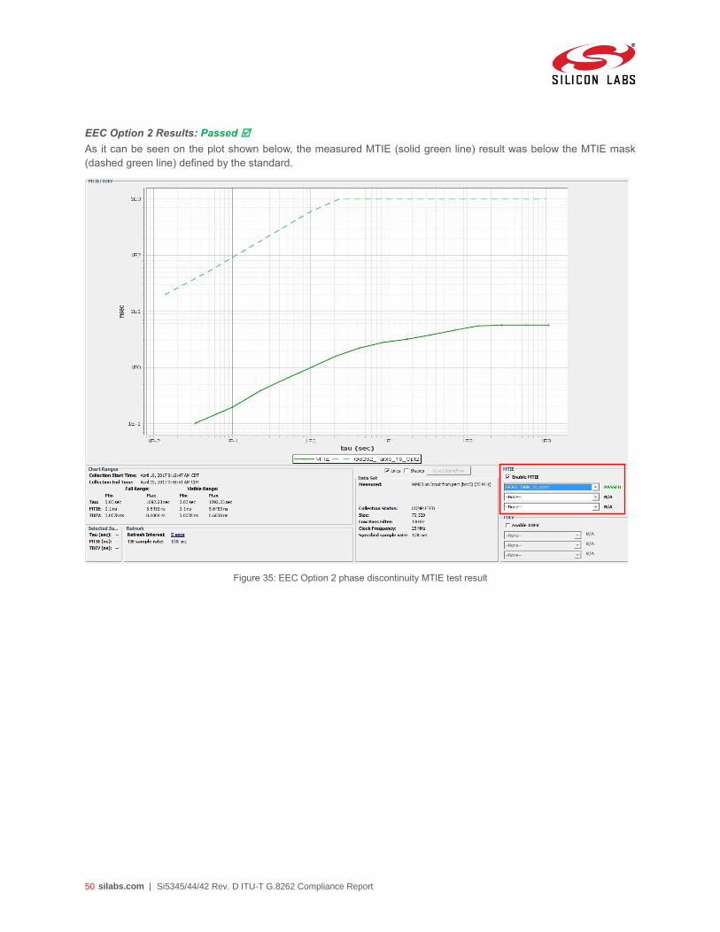
EEC Option 2 Results: Passed
As it can be seen on the plot shown below, the measured MTIE (solid green line) result was below the MTIE mask
(dashed green line) defined by the standard.
Figure 35: EEC Option 2 phase discontinuity MTIE test result
51 silabs.com | Si5345/44/42 Rev. D ITU-T G.8262 Compliance Report
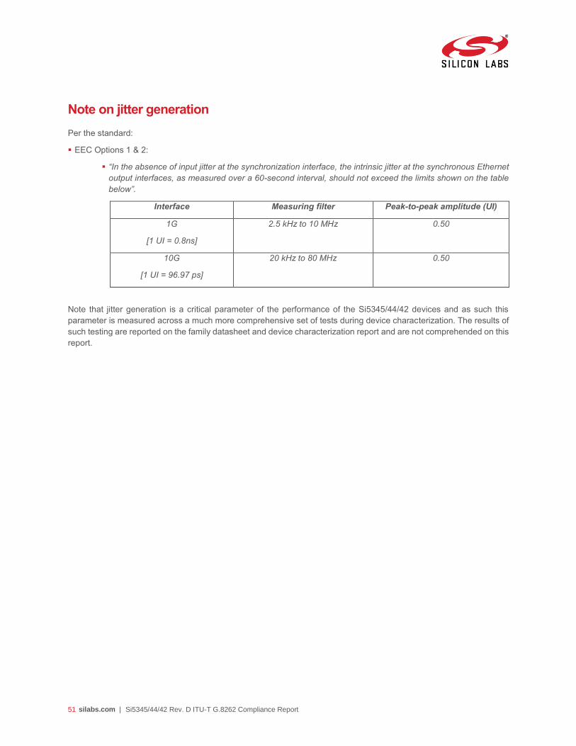
Note on jitter generation
Per the standard:
EEC Options 1 & 2:
“In the absence of input jitter at the synchronization interface, the intrinsic jitter at the synchronous Ethernet
output interfaces, as measured over a 60-second interval, should not exceed the limits shown on the table
below”.
Interface Measuring filter Peak-to-peak amplitude (UI)
1G
[1 UI = 0.8ns]
2.5 kHz to 10 MHz 0.50
10G
[1 UI = 96.97 ps]
20 kHz to 80 MHz 0.50
Note that jitter generation is a critical parameter of the performance of the Si5345/44/42 devices and as such this
parameter is measured across a much more comprehensive set of tests during device characterization. The results of
such testing are reported on the family datasheet and device characterization report and are not comprehended on this
report.