si4136/si4126 - silicon labs · table 5. rf and if synthesizer characteristics (vdd = 2.7 to 3.6 v,...
TRANSCRIPT

Rev. 1.42 Copyright © 2014 by Silicon Laboratories Si4136/Si4126This information applies to a product under development. Its characteristics and specifications are subject to change without notice.
Silicon Laboratories Confidential. Information contained herein is covered under non-disclosure agreement (NDA).
Si4136/Si4126
ISM RF SYNTHESIZER WITH INTEGRATED VCOS FOR WIRELESS COMMUNICATIONS
Features
Applications
Description
The Si4136 is a monolithic integrated circuit that performs both IF and RFsynthesis for wireless communications applications. The Si4136 includesthree VCOs, loop filters, reference and VCO dividers, and phase detectors.Divider and powerdown settings are programmable through a three-wireserial interface.
Functional Block Diagram
Dual-band RF synthesizersRF1: 2300 MHz to 2500 MHzRF2: 2025 MHz to 2300 MHz
IF synthesizer 62.5 MHz to 1000 MHz
Integrated VCOs, loop filters, varactors, and resonators
Minimal external components required
Low phase noise 5 µA standby current 25.7 mA typical supply current 2.7 V to 3.6 V operation Packages: 24-pin TSSOP,
28-lead QFNLead-free/RoHS-compliant options
available
ISM and MMDS band communications
Wireless LAN and WAN
Dual-band communications
IFOUT
IFLA
IFLB
RFOUT
XIN
PWDN
SDATA
SCLK
SEN
IF
RF2
RF1
AUXOUT
PhaseDetect
PhaseDetect
2
2
IFDIVPhaseDetect
TestMux
22-bitData
Register
SerialInterface
PowerDown
Control
ReferenceAmplifier RRF1
RRF2
RIF
NRF1
NRF2
NIF
÷1/÷2
Patents pending
Ordering Information:
See page 29.
Pin Assignments
Si4136-GT
Si4136-GM
SCLK
SDATA
GND
GND
NC
GND
NC
GND
GND
GND
RFOUT
VDDR
SEN
VDDI
IFOUT
GND
IFLB
IFLA
GND
VDDD
GND
XIN
PWDN
AUXOUT
1
2
3
4
5
6
7
8
9
10
11
12
24
23
22
21
20
19
18
17
16
15
14
13
SC
LK
SD
AT
A
GN
D
GND
NC
NC
GND
GND
RF
OU
T
VD
DR
SE
N
VD
DI
IFO
UT
GND
IFLB
IFLA
GN
D
VDDD
GND
XIN
PW
DN
AU
XO
UT
21
20
19
18
17
16
15
8 9 10 11 12 13 14
28 27 26 25 24 23 22
1
2
3
4
5
6
7
GN
D
GND
GND GND
GN
D
GN
D
GND

Si4136/Si4126
2 Rev. 1.42

Si4136/Si4126
Rev. 1.42 3
TABLE OF CONTENTS
Section Page
1. Electrical Specifications . . . . . . . . . . . . . . . . . . . . . . . . . . . . . . . . . . . . . . . . . . . . . . . . . . .42. Functional Description . . . . . . . . . . . . . . . . . . . . . . . . . . . . . . . . . . . . . . . . . . . . . . . . . . .16
2.1. Serial Interface . . . . . . . . . . . . . . . . . . . . . . . . . . . . . . . . . . . . . . . . . . . . . . . . . . . . .162.2. Setting the IF VCO Center Frequencies . . . . . . . . . . . . . . . . . . . . . . . . . . . . . . . . . .162.3. Self-Tuning Algorithm . . . . . . . . . . . . . . . . . . . . . . . . . . . . . . . . . . . . . . . . . . . . . . . .172.4. Output Frequencies . . . . . . . . . . . . . . . . . . . . . . . . . . . . . . . . . . . . . . . . . . . . . . . . . .172.5. PLL Loop Dynamics . . . . . . . . . . . . . . . . . . . . . . . . . . . . . . . . . . . . . . . . . . . . . . . . .182.6. RF and IF Outputs (RFOUT and IFOUT) . . . . . . . . . . . . . . . . . . . . . . . . . . . . . . . . .182.7. Reference Frequency Amplifier . . . . . . . . . . . . . . . . . . . . . . . . . . . . . . . . . . . . . . . . .192.8. Powerdown Modes . . . . . . . . . . . . . . . . . . . . . . . . . . . . . . . . . . . . . . . . . . . . . . . . . .192.9. Auxiliary Output (AUXOUT) . . . . . . . . . . . . . . . . . . . . . . . . . . . . . . . . . . . . . . . . . . .19
3. Control Registers . . . . . . . . . . . . . . . . . . . . . . . . . . . . . . . . . . . . . . . . . . . . . . . . . . . . . . . .214. Pin Descriptions: Si4136-GT . . . . . . . . . . . . . . . . . . . . . . . . . . . . . . . . . . . . . . . . . . . . . . .275. Pin Descriptions: Si4136-GM . . . . . . . . . . . . . . . . . . . . . . . . . . . . . . . . . . . . . . . . . . . . . .286. Ordering Guide . . . . . . . . . . . . . . . . . . . . . . . . . . . . . . . . . . . . . . . . . . . . . . . . . . . . . . . . . .297. Si4136 Derivative Devices . . . . . . . . . . . . . . . . . . . . . . . . . . . . . . . . . . . . . . . . . . . . . . . . .298. Package Outline: Si4136-GT . . . . . . . . . . . . . . . . . . . . . . . . . . . . . . . . . . . . . . . . . . . . . . .309. Package Outline: Si4136-GM . . . . . . . . . . . . . . . . . . . . . . . . . . . . . . . . . . . . . . . . . . . . . . .31Document Change List . . . . . . . . . . . . . . . . . . . . . . . . . . . . . . . . . . . . . . . . . . . . . . . . . . . . .32Contact Information . . . . . . . . . . . . . . . . . . . . . . . . . . . . . . . . . . . . . . . . . . . . . . . . . . . . . . . .34
Si4136/Si4126
4 Rev. 1.42
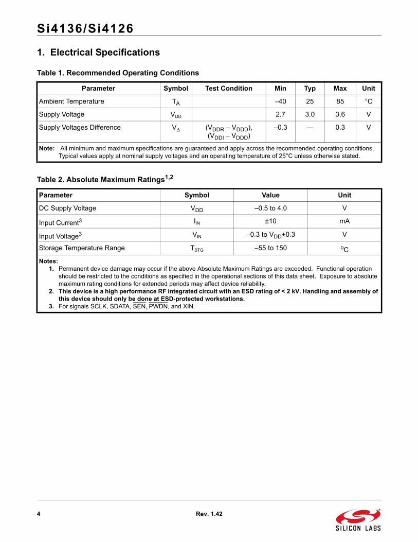
1. Electrical Specifications
Table 1. Recommended Operating Conditions
Parameter Symbol Test Condition Min Typ Max Unit
Ambient Temperature TA –40 25 85 °C
Supply Voltage VDD 2.7 3.0 3.6 V
Supply Voltages Difference V (VDDR – VDDD), (VDDI – VDDD)
–0.3 — 0.3 V
Note: All minimum and maximum specifications are guaranteed and apply across the recommended operating conditions. Typical values apply at nominal supply voltages and an operating temperature of 25°C unless otherwise stated.
Table 2. Absolute Maximum Ratings1,2
Parameter Symbol Value Unit
DC Supply Voltage VDD –0.5 to 4.0 V
Input Current3 IIN ±10 mA
Input Voltage3 VIN –0.3 to VDD+0.3 V
Storage Temperature Range TSTG –55 to 150 oC
Notes:1. Permanent device damage may occur if the above Absolute Maximum Ratings are exceeded. Functional operation
should be restricted to the conditions as specified in the operational sections of this data sheet. Exposure to absolute maximum rating conditions for extended periods may affect device reliability.
2. This device is a high performance RF integrated circuit with an ESD rating of < 2 kV. Handling and assembly of this device should only be done at ESD-protected workstations.
3. For signals SCLK, SDATA, SEN, PWDN, and XIN.

Si4136/Si4126
Rev. 1.42 5
Table 3. DC Characteristics (VDD = 2.7 to 3.6 V, TA = –40 to 85 °C)
Parameter Symbol Test Condition Min Typ Max Unit
Total Supply Current1 RF1 and IF operating — 25.7 31 mA
RF1 Mode Supply Current1 — 15.7 19 mA
RF2 Mode Supply Current1 — 15 18 mA
IF Mode Supply Current1 — 10 12 mA
Standby Current PWDN = 0 — 1 — µA
High Level Input Voltage2 VIH 0.7 VDD — — V
Low Level Input Voltage2 VIL — — 0.3 VDD V
High Level Input Current2 IIH VIH = 3.6 V,VDD = 3.6 V
–10 — 10 µA
Low Level Input Current2 IIL VIL = 0 V, VDD = 3.6 V
–10 — 10 µA
High Level Output Voltage3 VOH IOH = –500 µA VDD–0.4 — — V
Low Level Output Voltage3 VOL IOH = 500 µA — — 0.4 V
Notes:1. RF1 = 2.4 GHz, RF2 = 2.1 GHz, IFOUT = 800 MHz, LPWR = 0.2. For signals SCLK, SDATA, SEN, and PWDN.3. For signal AUXOUT.
Si4136/Si4126
6 Rev. 1.42
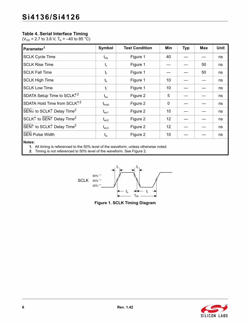
Figure 1. SCLK Timing Diagram
Table 4. Serial Interface Timing(VDD = 2.7 to 3.6 V, TA = –40 to 85 °C)
Parameter1 Symbol Test Condition Min Typ Max Unit
SCLK Cycle Time tclk Figure 1 40 — — ns
SCLK Rise Time tr Figure 1 — — 50 ns
SCLK Fall Time tf Figure 1 — — 50 ns
SCLK High Time th Figure 1 10 — — ns
SCLK Low Time tl Figure 1 10 — — ns
SDATA Setup Time to SCLK2 tsu Figure 2 5 — — ns
SDATA Hold Time from SCLK2 thold Figure 2 0 — — ns
SEN to SCLKDelay Time2 ten1 Figure 2 10 — — ns
SCLK to SENDelay Time2 ten2 Figure 2 12 — — ns
SEN to SCLKDelay Time2 ten3 Figure 2 12 — — ns
SEN Pulse Width tw Figure 2 10 — — ns
Notes:1. All timing is referenced to the 50% level of the waveform, unless otherwise noted.2. Timing is not referenced to 50% level of the waveform. See Figure 2.
SCLK80%
50%
20%
tr tf
th tltclk
Si4136/Si4126
Rev. 1.42 7
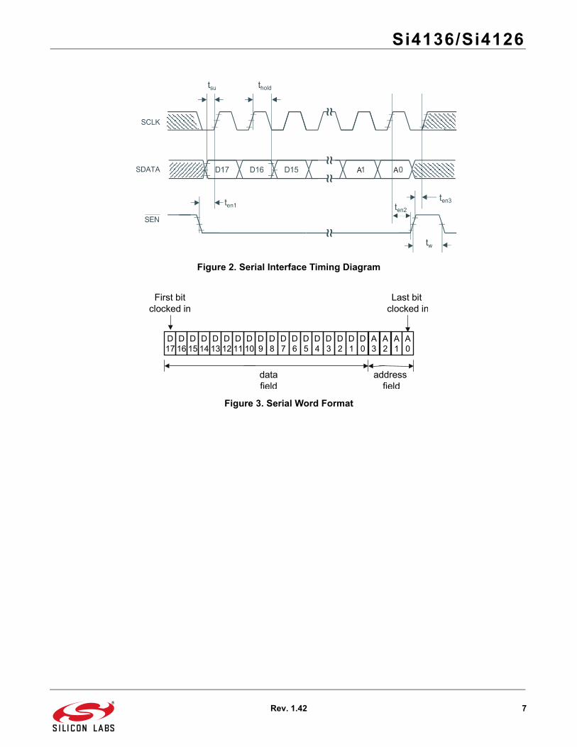
Figure 2. Serial Interface Timing Diagram
Figure 3. Serial Word Format
A A
D17
D16
D15
D14
D13
D12
D11
D10
D9
D8
D7
D6
D5
D4
D3
D2
D1
D0
A3
A2
A1
First bitclocked in
Last bit clocked in
address field
A0
datafield
Si4136/Si4126
8 Rev. 1.42
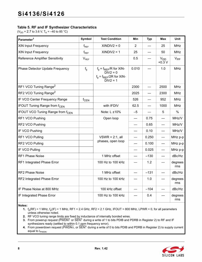
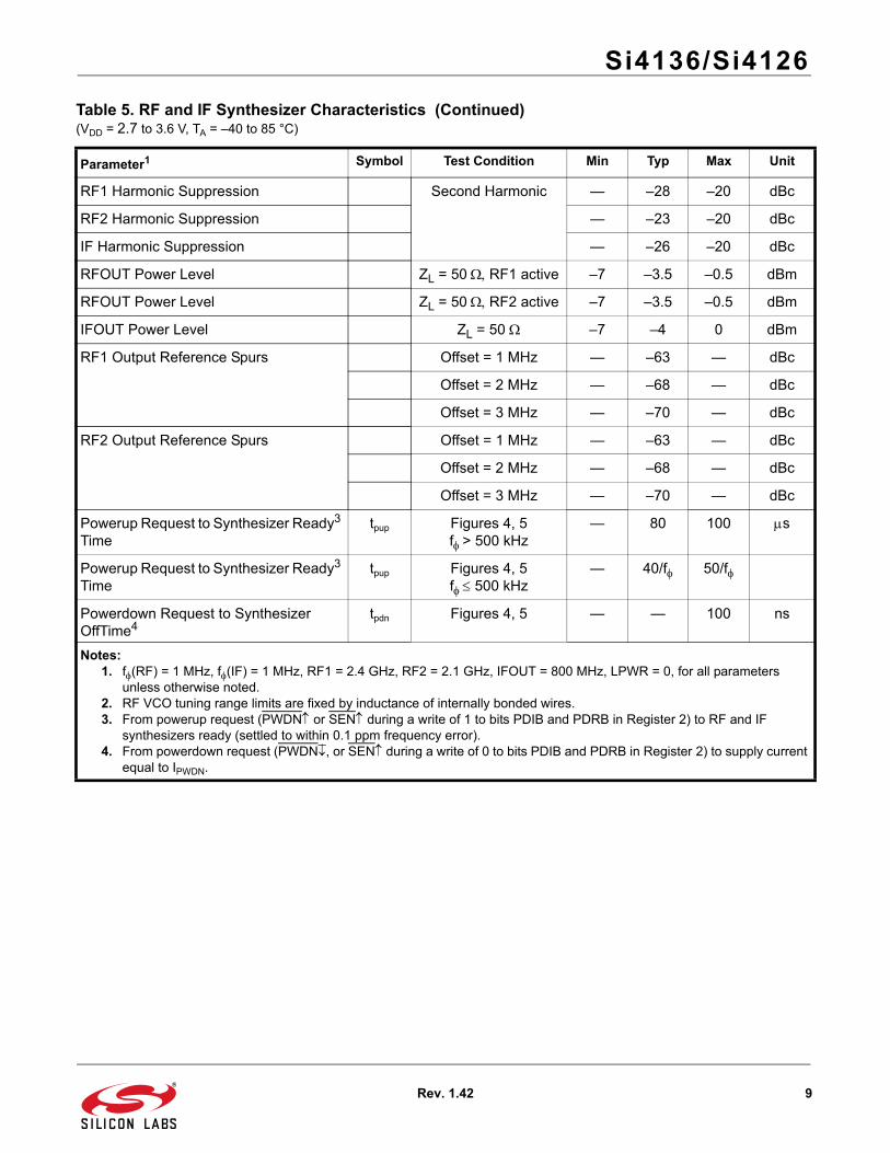
Table 5. RF and IF Synthesizer Characteristics (VDD = 2.7 to 3.6 V, TA = –40 to 85 °C)
Parameter1 Symbol Test Condition Min Typ Max Unit
XIN Input Frequency fREF XINDIV2 = 0 2 — 25 MHz
XIN Input Frequency fREF XINDIV2 = 1 25 — 50 MHz
Reference Amplifier Sensitivity VREF 0.5 — VDD +0.3 V
VPP
Phase Detector Update Frequency f f= fREF/R for XIN-DIV2 = 0
f= fREF/2R for XIN-DIV2 = 1
0.010 — 1.0 MHz
RF1 VCO Tuning Range2 2300 — 2500 MHz
RF2 VCO Tuning Range2 2025 — 2300 MHz
IF VCO Center Frequency Range fCEN 526 — 952 MHz
IFOUT Tuning Range from fCEN with IFDIV 62.5 — 1000 MHz
IFOUT VCO Tuning Range from fCEN Note: L ±10% –5 — 5 %
RF1 VCO Pushing Open loop — 0.75 — MHz/V
RF2 VCO Pushing — 0.65 — MHz/V
IF VCO Pushing — 0.10 — MHz/V
RF1 VCO Pulling VSWR = 2:1, all phases, open loop
— 0.250 — MHz p-p
RF2 VCO Pulling — 0.100 — MHz p-p
IF VCO Pulling — 0.025 — MHz p-p
RF1 Phase Noise 1 MHz offset — –130 — dBc/Hz
RF1 Integrated Phase Error 100 Hz to 100 kHz — 1.2 — degrees rms
RF2 Phase Noise 1 MHz offset — –131 — dBc/Hz
RF2 Integrated Phase Error 100 Hz to 100 kHz — 1.0 — degrees rms
IF Phase Noise at 800 MHz 100 kHz offset — –104 — dBc/Hz
IF Integrated Phase Error 100 Hz to 100 kHz — 0.4 — degrees rms
Notes:1. f(RF) = 1 MHz, f(IF) = 1 MHz, RF1 = 2.4 GHz, RF2 = 2.1 GHz, IFOUT = 800 MHz, LPWR = 0, for all parameters
unless otherwise noted.2. RF VCO tuning range limits are fixed by inductance of internally bonded wires.3. From powerup request (PWDN or SEN during a write of 1 to bits PDIB and PDRB in Register 2) to RF and IF
synthesizers ready (settled to within 0.1 ppm frequency error).4. From powerdown request (PWDN, or SENduring a write of 0 to bits PDIB and PDRB in Register 2) to supply current
equal to IPWDN.
Si4136/Si4126
Rev. 1.42 9
RF1 Harmonic Suppression Second Harmonic — –28 –20 dBc
RF2 Harmonic Suppression — –23 –20 dBc
IF Harmonic Suppression — –26 –20 dBc
RFOUT Power Level ZL = 50 RF1 active –7 –3.5 –0.5 dBm
RFOUT Power Level ZL = 50 RF2 active –7 –3.5 –0.5 dBm
IFOUT Power Level ZL = 50 –7 –4 0 dBm
RF1 Output Reference Spurs Offset = 1 MHz — –63 — dBc
Offset = 2 MHz — –68 — dBc
Offset = 3 MHz — –70 — dBc
RF2 Output Reference Spurs Offset = 1 MHz — –63 — dBc
Offset = 2 MHz — –68 — dBc
Offset = 3 MHz — –70 — dBc
Powerup Request to Synthesizer Ready3 Time
tpup Figures 4, 5f> 500 kHz
— 80 100 s
Powerup Request to Synthesizer Ready3 Time
tpup Figures 4, 5f 500 kHz
— 40/f 50/f
Powerdown Request to Synthesizer OffTime4
tpdn Figures 4, 5 — — 100 ns
Table 5. RF and IF Synthesizer Characteristics (Continued)(VDD = 2.7 to 3.6 V, TA = –40 to 85 °C)
Parameter1 Symbol Test Condition Min Typ Max Unit
Notes:1. f(RF) = 1 MHz, f(IF) = 1 MHz, RF1 = 2.4 GHz, RF2 = 2.1 GHz, IFOUT = 800 MHz, LPWR = 0, for all parameters
unless otherwise noted.2. RF VCO tuning range limits are fixed by inductance of internally bonded wires.3. From powerup request (PWDN or SEN during a write of 1 to bits PDIB and PDRB in Register 2) to RF and IF
synthesizers ready (settled to within 0.1 ppm frequency error).4. From powerdown request (PWDN, or SENduring a write of 0 to bits PDIB and PDRB in Register 2) to supply current
equal to IPWDN.

Si4136/Si4126
10 Rev. 1.42
Figure 4. Software Power Management Timing Diagram
Figure 5. Hardware Power Management Timing Diagram
PDIB = 0PDRB = 0
PDIB = 1PDRB = 1
tpup tpdnIT
IPWDN
SEN
SDATA
RF synthesizers settled to within0.1 ppm frequency error.
tpup tpdnIT
IPWDN
PWDN
RF synthesizers settled to within0.1 ppm frequency error.

Si4136/Si4126
Rev. 1.42 11
Figure 6. Typical Transient Response RF1 at 2.4 GHzwith 1 MHz Phase Detector Update Frequency

Si4136/Si4126
12 Rev. 1.42
Figure 7. Typical RF1 Phase Noise at 2.4 GHzwith 1 MHz Phase Detector Update Frequency
Figure 8. Typical RF1 Spurious Response at 2.4 GHzwith 1 MHz Phase Detector Update Frequency
Typical RF1 Phase Noise at 2.4 GHz
-140
-130
-120
-110
-100
-90
-80
-70
-60
1.E+02 1.E+03 1.E+04 1.E+05 1.E+06
Offset Frequency (Hz)
Pha
se N
oise
(dB
c/H
z)
Si4136/Si4126
Rev. 1.42 13
s
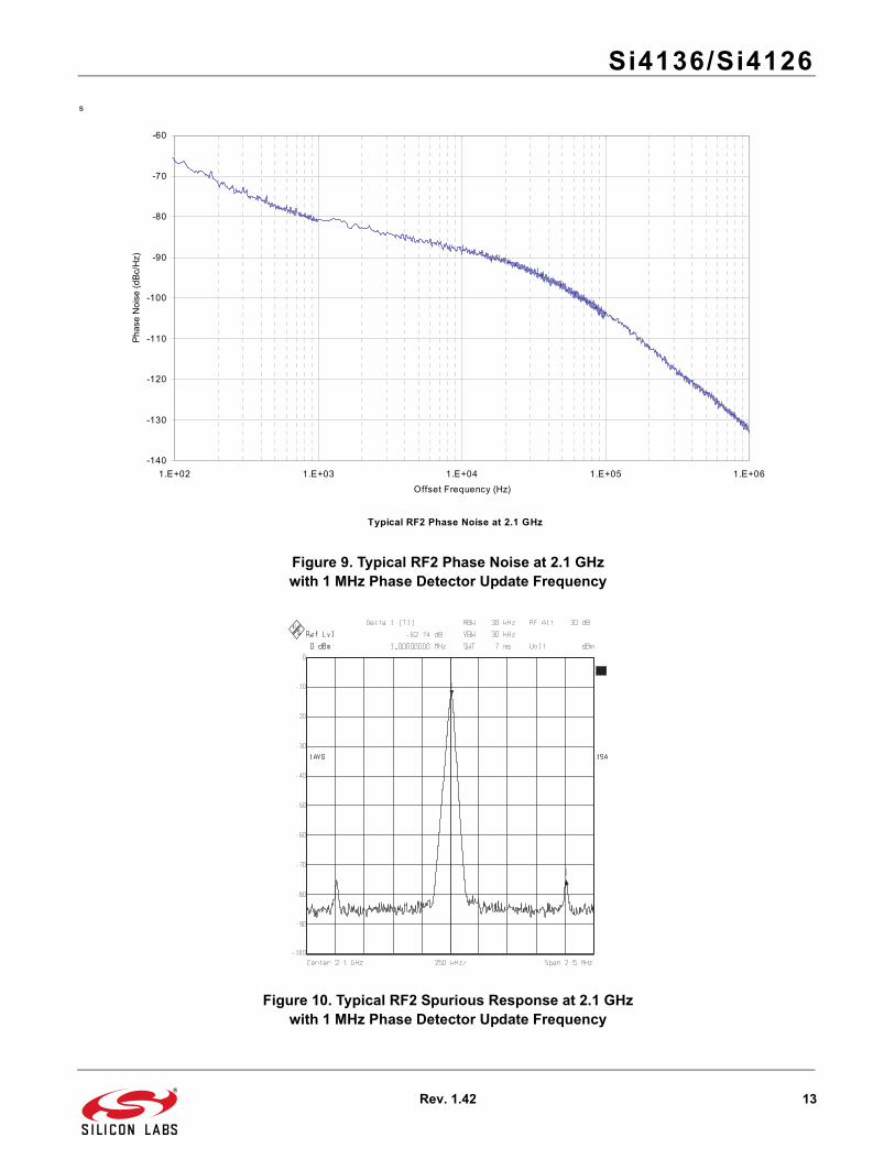
Figure 9. Typical RF2 Phase Noise at 2.1 GHzwith 1 MHz Phase Detector Update Frequency
Figure 10. Typical RF2 Spurious Response at 2.1 GHzwith 1 MHz Phase Detector Update Frequency
Typical RF2 Phase Noise at 2.1 GHz
-140
-130
-120
-110
-100
-90
-80
-70
-60
1.E+02 1.E+03 1.E+04 1.E+05 1.E+06
Offset Frequency (Hz)
Pha
se N
oise
(dB
c/H
z)

Si4136/Si4126
14 Rev. 1.42
Figure 11. Typical IF Phase Noise at 800 MHzwith 1 MHz Phase Detector Update Frequency
Figure 12. IF Spurious Response at 800 MHzwith 1 MHz Phase Detector Update Frequency
Typical IF Phase Noise at 800 MHz
-140
-130
-120
-110
-100
-90
-80
-70
-60
1.E+02 1.E+03 1.E+04 1.E+05 1.E+06
Offset Frequency (Hz)
Pha
se N
oise
(dB
c/H
z)
Si4136/Si4126
Rev. 1.42 15
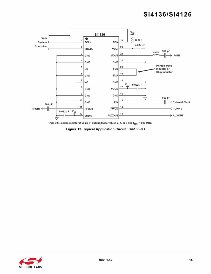
Figure 13. Typical Application Circuit: Si4136-GT
SCLK
SDATA
GND
GND
NC
GND
NC
GND
GND
GND
RFOUT
VDDR
SEN
VDDI
IFOUT
GND
IFLB
IFLA
GND
VDDD
GND
XIN
PWDN
AUXOUT
1
2
3
4
5
6
7
8
9
10
11
12
24
23
22
21
20
19
18
17
16
15
14
13
Si4136
RFOUT
560 pF
Printed TraceInductor orChip Inductor
IFOUT
560 pFLMATCH
AUXOUT
External Clock
560 pF
From
System
Controller0.022 F
VDD
0.022 F
0.022 FPDWNB
VDD
VDD
30
*Add 30 series resistor if using IF output divide values 2, 4, or 8 and fCEN < 600 MHz.
Si4136/Si4126
16 Rev. 1.42
2. Functional Description
The Si4136 is a monolithic integrated circuit thatperforms IF and dual-band RF synthesis for manywireless communications applications. This integratedcircuit (IC), along with a minimum number of externalcomponents, is all that is necessary to implement thefrequency synthesis function in applications like W-LANusing the IEEE 802.11 standard.
The Si4136 has three complete phase-locked loops(PLLs), with integrated voltage-controlled oscillators(VCOs). The low phase noise of the VCOs makes theSi4136 suitable for use in demanding wirelesscommunications applications. Also integrated are phasedetectors, loop filters, and reference and outputfrequency dividers. The IC is programmed through athree-wire serial interface.
Two PLLs are provided for RF synthesis. These RFPLLs are multiplexed so that only one PLL is active at agiven time (as determined by the setting of an internalregister). The active PLL is the last one written. Thecenter frequency of the VCO in each PLL is set by theinternal bond wire inductance within the package.Inaccuracies in these inductances are compensated forby the self-tuning algorithm. The algorithm is runfollowing power-up or following a change in theprogrammed output frequency.
The RF PLLs contain a divide-by-2 circuit before the N-divider. As a result, the phase detector frequency (f) isequal to half the desired channel spacing. For example,for a 200 kHz channel spacing, f would equal 100 kHz.The IF PLL does not contain the divide-by-2 circuitbefore the N-divider. In this case, f is equal to thedesired channel spacing. Each RF VCO is optimized fora particular frequency range. The RF1 VCO is optimizedto operate from 2.3 GHz to 2.5 GHz, while the RF2 VCOis optimized to operate between 2.025 GHz and2.3 GHz.
One PLL is provided for IF synthesis. The centerfrequency of this circuit’s VCO is set by an externalinductance. The PLL can adjust the IF output frequencyby ±5% of the VCO center frequency. Inaccuracies inthe value of the external inductance are compensatedfor by the Si4136’s proprietary self-tuning algorithm.This algorithm is initiated each time the PLL is powered-up (by either the PWDN pin or by software) and/or eachtime a new output frequency is programmed. The IFVCO can have its center frequency set as low as526 MHz and as high as 952 MHz. An IF output divideris provided to divide down the IF output frequencies, ifneeded. The divider is programmable, capable ofdividing by 1, 2, 4, or 8.
In order to accommodate designs running at XIN
frequencies greater than 25 MHz, the Si4136 includes aprogrammable divide-by-2 option (XINDIV2 inRegister 0, D6) on the XIN input. By enabling thisoption, the Si4136 can accept a range of TCXOfrequencies from 25 MHz to 50 MHz. This featuremakes the Si4136 ideal for W-LAN radio designsoperating at an XIN of 44 MHz.
The unique PLL architecture used in the Si4136produces settling (lock) times that are comparable inspeed to fractional-N architectures without suffering thehigh phase noise or spurious modulation effects oftenassociated with those designs.
2.1. Serial InterfaceA timing diagram for the serial interface is shown inFigure 2 on page 7. Figure 3 on page 7 shows theformat of the serial word.
The Si4136 is programmed serially with 22-bit wordscomprised of 18-bit data fields and 4-bit address fields.When the serial interface is enabled (i.e., when SEN islow) data and address bits on the SDATA pin areclocked into an internal shift register on the rising edgeof SCLK. Data in the shift register is then transferred onthe rising edge of SEN into the internal data registeraddressed in the address field. The serial interface isdisabled when SEN is high.
Table 11 on page 21 summarizes the data registerfunctions and addresses. It is not necessary (although itis permissible) to clock into the internal shift register anyleading bits that are “don’t cares.”
2.2. Setting the IF VCO Center FrequenciesThe IF PLL can adjust its output frequency ±5% fromthe center frequency as established by the value of anexternal inductance connected to the VCO. The RF1and RF2 PLLs have fixed operating ranges due to theinductance set by the internal bond wires. Each centerfrequency is established by the value of the totalinductance (internal and/or external) connected to therespective VCO. Manufacturing tolerance of ±10% forthe external inductor is acceptable for the IF VCO. TheSi4136 will compensate for inaccuracies by executing aself-tuning algorithm following PLL power-up orfollowing a change in the programmed outputfrequency.
Because the total tank inductance is in the low nHrange, the inductance of the package needs to beconsidered in determining the correct externalinductance. The total inductance (LTOT) presented tothe IF VCO is the sum of the external inductance (LEXT)and the package inductance (LPKG). The IF VCO has anominal capacitance (CNOM) in parallel with the totalinductance, and the center frequency is as follows:

Si4136/Si4126
Rev. 1.42 17
Table 6 summarizes the characteristics of the IF VCO.
Figure 14. Example of IF External Inductor
As a design example, suppose synthesizingfrequencies in a 30 MHz band between 735 MHz and765 MHz is desired. The center frequency should bedefined as midway between the two extremes, or750 MHz. The PLL will be able to adjust the VCO outputfrequency ±5% of the center frequency, or ±37.5 MHz of750 MHz (i.e., from approximately 713 MHz to788 MHz). The IF VCO has a CNOM of 6.5 pF, and a6.9 nH inductance (correct to two digits) in parallel withthis capacitance will yield the desired center frequency.An external inductance of 4.8 nH should be connectedbetween IFLA and IFLB, as shown in Figure 14. This, inaddition to 2.1 nH of package inductance, will presentthe correct total inductance to the VCO. Inmanufacturing, the external inductance can vary ±10%of its nominal value and the Si4136 will correct for thevariation with the self-tuning algorithm.
For more information on designing the external traceinductor, please refer to Application Note 31.
2.3. Self-Tuning AlgorithmThe self-tuning algorithm is initiated immediatelyfollowing power-up of a PLL or, if the PLL is alreadypowered, following a change in its programmed outputfrequency. This algorithm attempts to tune the VCO sothat its free-running frequency is near the desired outputfrequency. In so doing, the algorithm will compensatefor manufacturing tolerance errors in the value of theexternal inductance connected to the IF VCO. It will alsoreduce the frequency error for which the PLL mustcorrect to get the precise desired output frequency. Theself-tuning algorithm will leave the VCO oscillating at afrequency in error by somewhat less than 1% of thedesired output frequency.
After self-tuning, the PLL controls the VCO oscillationfrequency. The PLL will complete frequency locking,eliminating any remaining frequency error. Thereafter, itwill maintain frequency-lock, compensating for effectscaused by temperature and supply voltage variations.
The Si4136’s self-tuning algorithm will compensate forcomponent value errors at any temperature within thespecified temperature range. However, the ability of thePLL to compensate for drift in component values thatoccur after self-tuning is limited. For externalinductances with temperature coefficients around ±150ppm/°C, the PLL will be able to maintain lock forchanges in temperature of approximately ±30°C.
Applications where the PLL is regularly powered-downor the frequency is periodically reprogrammed minimizeor eliminate the potential effects of temperature driftbecause the VCO is re-tuned in either case. Inapplications where the ambient temperature can driftsubstantially after self-tuning, it may be necessary tomonitor the lock-detect bar (LDETB) signal on theAUXOUT pin to determine whether a PLL is about torun out of locking capability. (See “2.9. Auxiliary Output(AUXOUT)” for how to select LDETB.) The LDETBsignal will be low after self-tuning has completed but willrise when either the IF or RF PLL nears the limit of itscompensation range. (LDETB will also be high wheneither PLL is executing the self-tuning algorithm.) Theoutput frequency will still be locked when LDETB goeshigh, but the PLL will eventually lose lock if thetemperature continues to drift in the same direction.Therefore, if LDETB goes high both the IF and RF PLLsshould promptly be re-tuned by initiating the self-tuningalgorithm.
2.4. Output FrequenciesThe IF and RF output frequencies are set byprogramming the R- and N-Divider registers. Each PLLhas its own R and N registers so that each can be
Table 6. Si4136-GT VCO Characteristics
VCO Fcen Range (MHz)
Cnom (pF)
Lpkg (nH)
Lext Range (nH)
Min Max Min Max
IF 526 952 6.5 2.1 2.2 12.0
fCEN1
2 LTOT CNOM--------------------------------------------- 1
2 LPKG LEXT+ CNOM----------------------------------------------------------------------= =
Si4136
LPKG
2
LPKG
2
LEXT
IFLB
IFLA
Si4136/Si4126
18 Rev. 1.42
programmed independently. Programming either the R-or N-Divider register for RF1 or RF2 automaticallyselects the associated output.
When XINDIV2 = 0, the reference frequency on the XINpin is divided by R and this signal is the input to thePLL’s phase detector. The other input to the phasedetector is the PLL’s VCO output frequency divided by2N for the RF PLLs or N for the IF PLL. After an initialtransient
Equation 1. fOUT = (2N/R) fREF (for the RF PLLs)
Equation 2. fOUT = (N/R) fREF (for the IF PLL).
The integers R are set by programming the RF1 R-Divider register (Register 6), the RF2 R-Divider register(Register 7) and the IF R-Divider register (Register 8).
The integers N are set by programming the RF1 N-Divider register (register 3), the RF2 N-Divider register(Register 4), and the IF N-Divider register (Register 5).
If the optional divide-by-2 circuit on the XIN pin isenabled (XINDIV2 = 1) then after an initial transient
fOUT = (N/R) fREF (for the RF PLLs)
fOUT = (N/2R) fREF (for the IF PLL).
Each N-Divider is implemented as a conventional highspeed divider. That is, it consists of a dual-modulusprescaler, a swallow counter, and a lower speedsynchronous counter. However, the control of thesesub-circuits is handled automatically. Only theappropriate N value should be programmed.
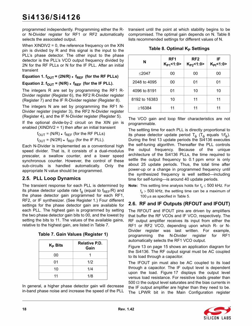
2.5. PLL Loop DynamicsThe transient response for each PLL is determined byits phase detector update rate f (equal to fREF/R) andthe phase detector gain programmed for each RF1,RF2, or IF synthesizer. (See Register 1.) Four differentsettings for the phase detector gain are available foreach PLL. The highest gain is programmed by settingthe two phase detector gain bits to 00, and the lowest bysetting the bits to 11. The values of the available gains,relative to the highest gain, are listed in Table 7.
In general, a higher phase detector gain will decreasein-band phase noise and increase the speed of the PLL
transient until the point at which stability begins to becompromised. The optimal gain depends on N. Table 8lists recommended settings for different values of N.
The VCO gain and loop filter characteristics are notprogrammable.
The settling time for each PLL is directly proportional toits phase detector update period T (T equals 1/f).During the first 13 update periods the Si4136 executesthe self-tuning algorithm. Thereafter the PLL controlsthe output frequency. Because of the uniquearchitecture of the Si4136 PLLs, the time required tosettle the output frequency to 0.1 ppm error is onlyabout 25 update periods. Thus, the total time afterpower-up or a change in programmed frequency untilthe synthesized frequency is well settled—includingtime for self-tuning—is around 40 update periods.
Note: This settling time analysis holds for f 500 kHz. For
f 500 kHz, the settling time can be a maximum of
100 s as specified in Table 5.
2.6. RF and IF Outputs (RFOUT and IFOUT)The RFOUT and IFOUT pins are driven by amplifiersthat buffer the RF VCOs and IF VCO, respectively. TheRF output amplifier receives its input from either theRF1 or RF2 VCO, depending upon which R- or N-Divider register was last written. For example,programming the N-Divider register for RF1automatically selects the RF1 VCO output.
Figure 13 on page 15 shows an application diagram forthe Si4136. The RF output signal must be AC coupledto its load through a capacitor.
The IFOUT pin must also be AC coupled to its loadthrough a capacitor. The IF output level is dependentupon the load. Figure 17 displays the output levelversus load resistance. For resistive loads greater than500 the output level saturates and the bias currents inthe IF output amplifier are higher than they need to be.The LPWR bit in the Main Configuration register
Table 7. Gain Values (Register 1)
KP Bits Relative P.D. Gain
00 1
01 1/2
10 1/4
11 1/8
Table 8. Optimal KP Settings
NRF1
KP1<1:0>RF2
KP2<1:0>IF
KPI<1:0>
2047 00 00 00
2048 to 4095 00 01 01
4096 to 8191 01 10 10
8192 to 16383 10 11 11
16384 11 11 11
Si4136/Si4126
Rev. 1.42 19
(Register 0) can be set to 1 to reduce the bias currentsand therefore reduce the power dissipated by the IFamplifier. For loads less than 500 LPWR should beset to 0 to maximize the output level.
For IF frequencies greater than 500 MHz, a matchingnetwork is required in order to drive a 50 load. SeeFigure 15 below. The value of LMATCH can bedetermined by Table 9.
Typical values range between 8 nH and 40 nH.
Figure 15. IF Frequencies > 500 MHz
For frequencies less than 500 MHz, the IF output buffercan directly drive a 200 resistive load or higher. Forresistive loads greater than 500 (f < 500 MHz) theLPWR bit can be set to reduce the power consumed bythe IF output buffer. See Figure 16 below.
Figure 16. IF Frequencies < 500 MHz
Figure 17. Typical IF Output Voltage vs.Load Resistance at 550 MHz
2.7. Reference Frequency AmplifierThe Si4136 provides a reference frequency amplifier. Ifthe driving signal has CMOS levels, it can be connecteddirectly to the XIN pin. Otherwise, the referencefrequency signal should be AC coupled to the XIN pinthrough a 560 pF capacitor.
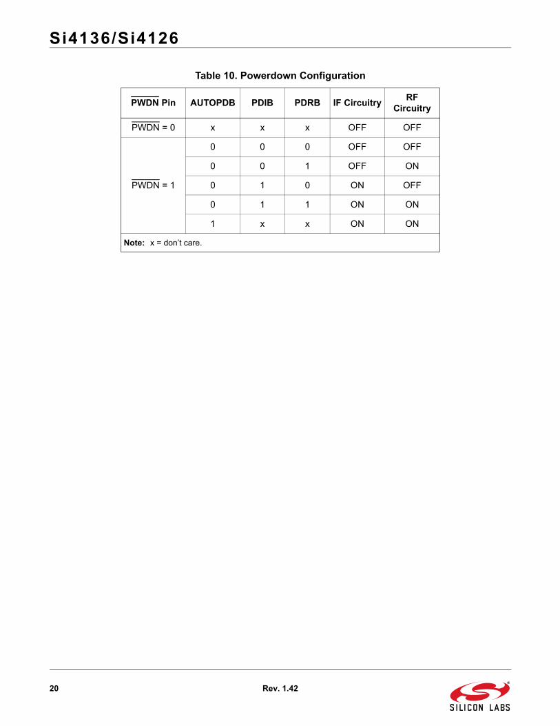
2.8. Powerdown ModesTable 10 summarizes the powerdown functionality. TheSi4136 can be powered down by taking the PWDN pinlow or by setting bits in the Powerdown register(Register 2). When the PWDN pin is low, the Si4136 willbe powered down regardless of the Powerdown registersettings. When the PWDN pin is high, powermanagement is under control of the Powerdown registerbits.
The IF and RF sections of the Si4136 circuitry can beindividually powered down by setting the Powerdownregister bits PDIB and PDRB low. The referencefrequency amplifier will also be powered up if either thePDRB and PDIB bits are high. Also, setting theAUTOPDB bit to 1 in the Main Configuration register(Register 0) is equivalent to setting both bits in thePowerdown register to 1.
The serial interface remains available and can bewritten in all power-down modes.
2.9. Auxiliary Output (AUXOUT)The signal appearing on AUXOUT is selected by settingthe AUXSEL bits in the Main Configuration register(Register 0).
The LDETB signal can be selected by setting theAUXSEL bits to 011. This signal can be used to indicatethat the IF or RF PLL is about to lose lock due toexcessive ambient temperature drift and should be re-tuned.
Table 9. LMATCH Values
Frequency LMATCH
500–600 MHz 40 nH
600–800 MHz 27 nH
800–1 GHz 18 nH
IFOUT
LMATCH
>500 pF
50
IFOUT>500 pF
>200
0
50
100
150
200
250
300
350
400
450
0 200 400 600 800 1000 1200
Load Resistance ()
Ou
tpu
t V
olt
ag
e (
mV
rms
)
LPWR=0
LPWR=1
Si4136/Si4126
20 Rev. 1.42
Table 10. Powerdown Configuration
PWDN Pin AUTOPDB PDIB PDRB IF CircuitryRF
Circuitry
PWDN = 0 x x x OFF OFF
PWDN = 1
0 0 0 OFF OFF
0 0 1 OFF ON
0 1 0 ON OFF
0 1 1 ON ON
1 x x ON ON
Note: x = don’t care.
Si4136/Si4126
Rev. 1.42 21
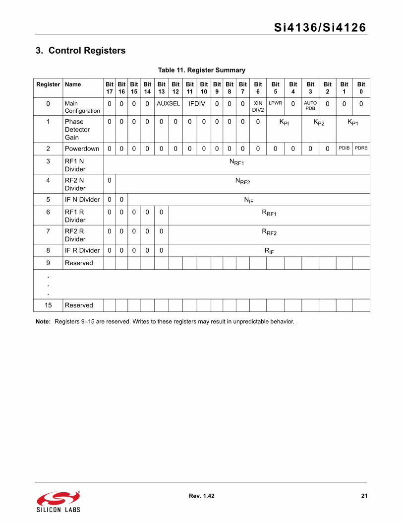
3. Control Registers
Note: Registers 9–15 are reserved. Writes to these registers may result in unpredictable behavior.
Table 11. Register Summary
Register Name Bit 17
Bit 16
Bit 15
Bit 14
Bit 13
Bit 12
Bit 11
Bit 10
Bit 9
Bit 8
Bit 7
Bit 6
Bit 5
Bit 4
Bit3
Bit 2
Bit 1
Bit 0
0 Main Configuration
0 0 0 0 AUXSEL IFDIV 0 0 0 XINDIV2
LPWR 0 AUTOPDB
0 0 0
1 Phase Detector Gain
0 0 0 0 0 0 0 0 0 0 0 0 KPI KP2 KP1
2 Powerdown 0 0 0 0 0 0 0 0 0 0 0 0 0 0 0 0 PDIB PDRB
3 RF1 N Divider
NRF1
4 RF2 N Divider
0 NRF2
5 IF N Divider 0 0 NIF
6 RF1 R Divider
0 0 0 0 0 RRF1
7 RF2 R Divider
0 0 0 0 0 RRF2
8 IF R Divider 0 0 0 0 0 RIF
9 Reserved
.
.
.
15 Reserved
Si4136/Si4126
22 Rev. 1.42
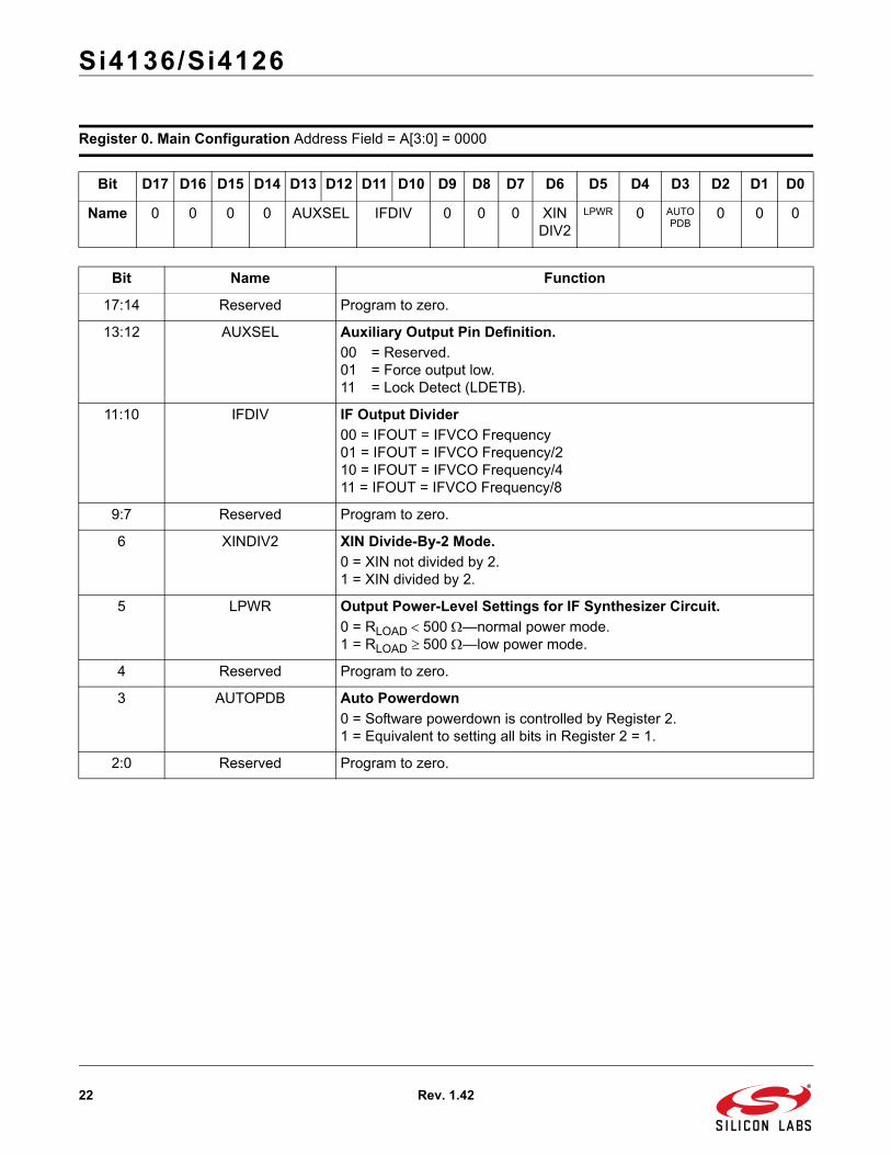
Register 0. Main Configuration Address Field = A[3:0] = 0000
Bit D17 D16 D15 D14 D13 D12 D11 D10 D9 D8 D7 D6 D5 D4 D3 D2 D1 D0
Name 0 0 0 0 AUXSEL IFDIV 0 0 0 XINDIV2
LPWR 0 AUTOPDB
0 0 0
Bit Name Function
17:14 Reserved Program to zero.
13:12 AUXSEL Auxiliary Output Pin Definition.
00 = Reserved.01 = Force output low.11 = Lock Detect (LDETB).
11:10 IFDIV IF Output Divider
00 = IFOUT = IFVCO Frequency01 = IFOUT = IFVCO Frequency/210 = IFOUT = IFVCO Frequency/411 = IFOUT = IFVCO Frequency/8
9:7 Reserved Program to zero.
6 XINDIV2 XIN Divide-By-2 Mode.
0 = XIN not divided by 2.1 = XIN divided by 2.
5 LPWR Output Power-Level Settings for IF Synthesizer Circuit.
0 = RLOAD 500 —normal power mode.1 = RLOAD 500 —low power mode.
4 Reserved Program to zero.
3 AUTOPDB Auto Powerdown
0 = Software powerdown is controlled by Register 2.1 = Equivalent to setting all bits in Register 2 = 1.
2:0 Reserved Program to zero.
Si4136/Si4126
Rev. 1.42 23
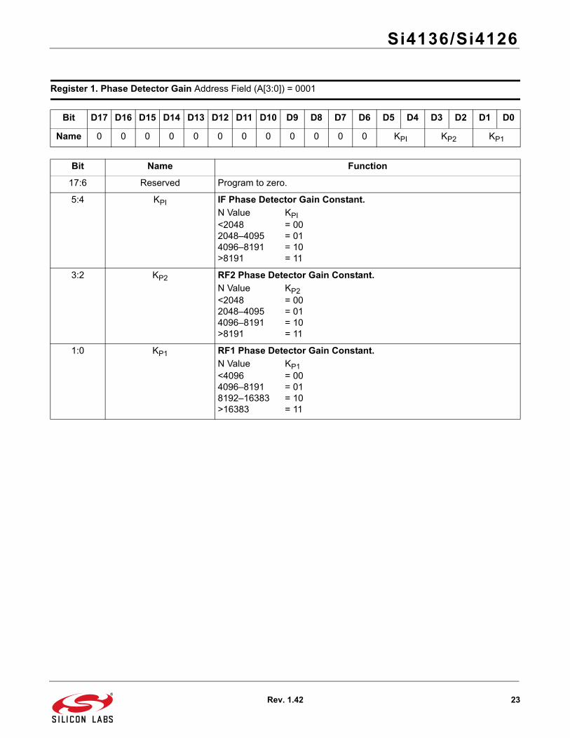
Register 1. Phase Detector Gain Address Field (A[3:0]) = 0001
Bit D17 D16 D15 D14 D13 D12 D11 D10 D9 D8 D7 D6 D5 D4 D3 D2 D1 D0
Name 0 0 0 0 0 0 0 0 0 0 0 0 KPI KP2 KP1
Bit Name Function
17:6 Reserved Program to zero.
5:4 KPI IF Phase Detector Gain Constant.
N Value KPI<2048 = 002048–4095 = 014096–8191 = 10>8191 = 11
3:2 KP2 RF2 Phase Detector Gain Constant.
N Value KP2<2048 = 002048–4095 = 014096–8191 = 10>8191 = 11
1:0 KP1 RF1 Phase Detector Gain Constant.
N Value KP1<4096 = 004096–8191 = 018192–16383 = 10>16383 = 11
Si4136/Si4126
24 Rev. 1.42
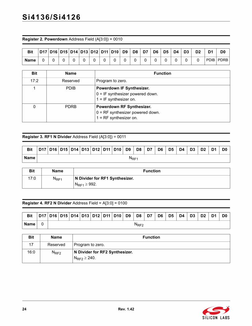
Register 2. Powerdown Address Field (A[3:0]) = 0010
Bit D17 D16 D15 D14 D13 D12 D11 D10 D9 D8 D7 D6 D5 D4 D3 D2 D1 D0
Name 0 0 0 0 0 0 0 0 0 0 0 0 0 0 0 0 PDIB PDRB
Bit Name Function
17:2 Reserved Program to zero.
1 PDIB Powerdown IF Synthesizer.
0 = IF synthesizer powered down.1 = IF synthesizer on.
0 PDRB Powerdown RF Synthesizer.
0 = RF synthesizer powered down.1 = RF synthesizer on.
Register 3. RF1 N Divider Address Field (A[3:0]) = 0011
Bit D17 D16 D15 D14 D13 D12 D11 D10 D9 D8 D7 D6 D5 D4 D3 D2 D1 D0
Name NRF1
Bit Name Function
17:0 NRF1 N Divider for RF1 Synthesizer.
NRF1 992.
Register 4. RF2 N Divider Address Field = A[3:0] = 0100
Bit D17 D16 D15 D14 D13 D12 D11 D10 D9 D8 D7 D6 D5 D4 D3 D2 D1 D0
Name 0 NRF2
Bit Name Function
17 Reserved Program to zero.
16:0 NRF2 N Divider for RF2 Synthesizer.
NRF2 240.

Si4136/Si4126
Rev. 1.42 25
Register 5. IF N Divider Address Field (A[3:0]) = 0101
Bit D17 D16 D15 D14 D13 D12 D11 D10 D9 D8 D7 D6 D5 D4 D3 D2 D1 D0
Name 0 0 NIF
Bit Name Function
17:16 Reserved Program to zero.
15:0 NIF N Divider for IF Synthesizer.
NIF 56.
Register 6. RF1 R Divider Address Field (A[3:0]) = 0110
Bit D17 D16 D15 D14 D13 D12 D11 D10 D9 D8 D7 D6 D5 D4 D3 D2 D1 D0
Name 0 0 0 0 0 RRF1
Name Function
17:13 Reserved Program to zero.
12:0 RRF1 R Divider for RF1 Synthesizer.
RRF1 can be any value from 7 to 8189 if KP1 = 008 to 8189 if KP1 = 0110 to 8189 if KP1 = 1014 to 8189 if KP1 = 11
Register 7. RF2 R Divider Address Field (A[3:0]) = 0111
Bit D17 D16 D15 D14 D13 D12 D11 D10 D9 D8 D7 D6 D5 D4 D3 D2 D1 D0
Name 0 0 0 0 0 RRF2
Bit Name Function
17:13 Reserved Program to zero.
12:0 RRF2 R Divider for RF2 Synthesizer.
RRF2 can be any value from 7 to 8189 if KP2 = 008 to 8189 if KP2 = 01 10 to 8189 if KP2 = 10 14 to 8189 if KP2 = 11
Si4136/Si4126
26 Rev. 1.42
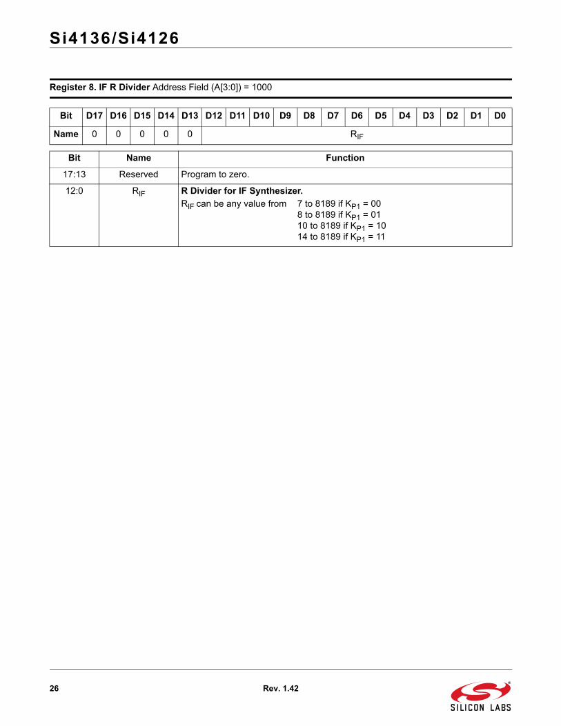
Register 8. IF R Divider Address Field (A[3:0]) = 1000
Bit D17 D16 D15 D14 D13 D12 D11 D10 D9 D8 D7 D6 D5 D4 D3 D2 D1 D0
Name 0 0 0 0 0 RIF
Bit Name Function
17:13 Reserved Program to zero.
12:0 RIF R Divider for IF Synthesizer.
RIF can be any value from 7 to 8189 if KP1 = 008 to 8189 if KP1 = 0110 to 8189 if KP1 = 1014 to 8189 if KP1 = 11

Si4136/Si4126
Rev. 1.42 27
4. Pin Descriptions: Si4136-GT
Pin Number(s) Name Description
1 SCLK Serial clock input
2 SDATA Serial data input
3, 4, 6, 8–10, 16, 18, 21
GND Common ground
5, 7 NC No connect
11 RFOUT Radio frequency (RF) output of the selected RF VCO
12 VDDR Supply voltage for the RF analog circuitry
13 AUXOUT Auxiliary output
14 PWDN Powerdown input pin
15 XIN Reference frequency amplifier input
17 VDDD Supply voltage for digital circuitry
19, 20 IFLA, IFLB Pins for inductor connection to IF VCO
22 IFOUT Intermediate frequency (IF) output of the IF VCO
23 VDDI Supply voltage for IF analog circuitry
24 SEN Enable serial port input
SCLK
SDATA
GND
GND
NC
GND
NC
GND
GND
GND
RFOUT
VDDR
SEN
VDDI
IFOUT
GND
IFLB
IFLA
GND
VDDD
GND
XIN
PWDN
AUXOUT
1
2
3
4
5
6
7
8
9
10
11
12
24
23
22
21
20
19
18
17
16
15
14
13

Si4136/Si4126
28 Rev. 1.42
5. Pin Descriptions: Si4136-GM
Pin Number(s) Name Description
1, 2, 4, 6, 7–9, 14, 16, 18, 21, 22, 28
GND Common ground
3, 5 NC No connect
10 RFOUT Radio frequency (RF) output of the selected RF VCO
11 VDDR Supply voltage for the RF analog circuitry
12 AUXOUT Auxiliary output
13 PWDN Powerdown input pin
15 XIN Reference frequency amplifier input
17 VDDD Supply voltage for digital circuitry
19, 20 IFLA, IFLB Pins for inductor connection to IF VCO
23 IFOUT Intermediate frequency (IF) output of the IF VCO
24 VDDI Supply voltage for IF analog circuitry
25 SEN Enable serial port input
26 SCLK Serial clock input
27 SDATA Serial data input
SC
LK
SD
AT
A
GN
D
GND
NC
NC
GND
GND
RF
OU
T
VD
DR
SE
N
VD
DI
IFO
UT
GND
IFLB
IFLA
GN
D
VDDD
GND
XIN
PW
DN
AU
XO
UT
21
20
19
18
17
16
15
8 9 10 11 12 13 14
28 27 26 25 24 23 22
1
2
3
4
5
6
7
GN
D
GND
GND GND
GN
D
GN
D
GND

Si4136/Si4126
Rev. 1.42 29
6. Ordering Guide
7. Si4136 Derivative Devices
The Si4136 performs both IF and dual-band RF frequency synthesis. The Si4126 is a derivative of this device. TheSi4126 features two synthesizers, RF2 and IF; it does not include RF1. The pinouts for the Si4126 and the Si4136are the same. Unused registers related to RF1 should be programmed to zero.
Ordering Part Number
Description Lead-Free/RoHS Compliant
Temperature
Si4136-F-GT 2.5 GHz/2.3 GHz/IF OUT/Lead Free –40 to 85 oC
Si4136-F-GM 2.5 GHz/2.3 GHz/IF OUT/Lead Free –40 to 85 oC
Si4126-F-GM 2.3 GHz/IF OUT/Lead Free –40 to 85 oC
Si4136/Si4126
30 Rev. 1.42
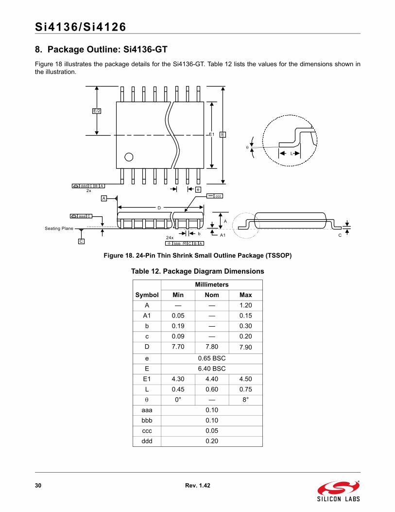
8. Package Outline: Si4136-GT
Figure 18 illustrates the package details for the Si4136-GT. Table 12 lists the values for the dimensions shown inthe illustration.
Figure 18. 24-Pin Thin Shrink Small Outline Package (TSSOP)
Table 12. Package Diagram Dimensions
Symbol
Millimeters
Min Nom Max
A — — 1.20
A1 0.05 — 0.15
b 0.19 — 0.30
c 0.09 — 0.20
D 7.70 7.80 7.90
e 0.65 BSC
E 6.40 BSC
E1 4.30 4.40 4.50
L 0.45 0.60 0.75
0° — 8°
aaa 0.10
bbb 0.10
ccc 0.05
ddd 0.20
E1 E
e
D
L
C
A
A1b
E/2
bbb C B AM
2xddd C B A
Accc
24x
aaa C
Seating Plane
C
Si4136/Si4126
Rev. 1.42 31
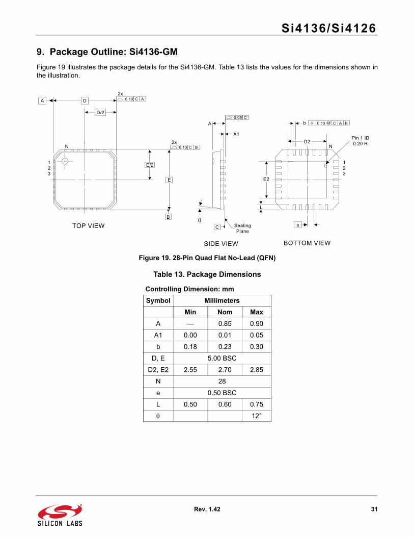
9. Package Outline: Si4136-GM
Figure 19 illustrates the package details for the Si4136-GM. Table 13 lists the values for the dimensions shown inthe illustration.
Figure 19. 28-Pin Quad Flat No-Lead (QFN)
Table 13. Package Dimensions
Controlling Dimension: mm
Symbol Millimeters
Min Nom Max
A — 0.85 0.90
A1 0.00 0.01 0.05
b 0.18 0.23 0.30
D, E 5.00 BSC
D2, E2 2.55 2.70 2.85
N 28
e 0.50 BSC
L 0.50 0.60 0.75
12°
E/2
E
A
N
D/2
D
A1
A b
N
e
L
BOTTOM VIEW
TOP VIEW
123
123
Pin 1 ID0.20 RD2
E2
B
0.10 C A2x
0.10 C B2x
C
0.05 C
Seating Plane
0.10 C A BM
SIDE VIEW

Si4136/Si4126
32 Rev. 1.42
DOCUMENT CHANGE LIST
Revision 1.3 to Revision 1.4 Si4136-BT change to Si4136-BT/GT
Si4136-BM change to Si4136-BM/GM
Revision 1.4 to Revision 1.41 Updated contact information.
Revision 1.41 to Revision 1.42 Si4136-F-BT removed from document.
Si4136-F-BM removed from document.
Si4126-F-BM removed from document.

Si4136/Si4126
Rev. 1.42 33
NOTES:

DisclaimerSilicon Laboratories intends to provide customers with the latest, accurate, and in-depth documentation of all peripherals and modules available for system and software implementers using or intending to use the Silicon Laboratories products. Characterization data, available modules and peripherals, memory sizes and memory addresses refer to each specific device, and "Typical" parameters provided can and do vary in different applications. Application examples described herein are for illustrative purposes only. Silicon Laboratories reserves the right to make changes without further notice and limitation to product information, specifications, and descriptions herein, and does not give warranties as to the accuracy or completeness of the included information. Silicon Laboratories shall have no liability for the consequences of use of the information supplied herein. This document does not imply or express copyright licenses granted hereunder to design or fabricate any integrated circuits. The products must not be used within any Life Support System without the specific written consent of Silicon Laboratories. A "Life Support System" is any product or system intended to support or sustain life and/or health, which, if it fails, can be reasonably expected to result in significant personal injury or death. Silicon Laboratories products are generally not intended for military applications. Silicon Laboratories products shall under no circumstances be used in weapons of mass destruction including (but not limited to) nuclear, biological or chemical weapons, or missiles capable of delivering such weapons.
Trademark InformationSilicon Laboratories Inc., Silicon Laboratories, Silicon Labs, SiLabs and the Silicon Labs logo, CMEMS®, EFM, EFM32, EFR, Energy Micro, Energy Micro logo and combinations thereof, "the world’s most energy friendly microcontrollers", Ember®, EZLink®, EZMac®, EZRadio®, EZRadioPRO®, DSPLL®, ISOmodem ®, Precision32®, ProSLIC®, SiPHY®, USBXpress® and others are trademarks or registered trademarks of Silicon Laboratories Inc. ARM, CORTEX, Cortex-M3 and THUMB are trademarks or registered trademarks of ARM Holdings. Keil is a registered trademark of ARM Limited. All other products or brand names mentioned herein are trademarks of their respective holders.
http://www.silabs.com
Silicon Laboratories Inc.400 West Cesar ChavezAustin, TX 78701USA
Simplicity StudioOne-click access to MCU tools, documentation, software, source code libraries & more. Available for Windows, Mac and Linux!
www.silabs.com/simplicity
MCU Portfoliowww.silabs.com/mcu
SW/HWwww.silabs.com/simplicity
Qualitywww.silabs.com/quality
Support and Communitycommunity.silabs.com