si3406x family data sheet - silicon labs · si3406x family data sheet fully-integrated ieee...
TRANSCRIPT

Si3406x Family Data Sheet
Fully-Integrated IEEE 802.3-Compliant POE+ PD Interface andHigh-Efficiency Switching Regulators with Transistor Bypass,Sleep, Wake, and LED DriveThe Si3406x family integrates all power management and control functions required ina Power-over-Ethernet Plus (PoE+) powered device (PD) application. These devicesconvert the high voltage supplied over the 10/100/1000BASE-T Ethernet connection toa regulated, low-voltage output supply. The optimized architecture of this device familyminimizes the solution footprint and external BOM cost and enables the use of low-costexternal components while maintaining high performance. The Si3406x family integra-tes the required diode bridges and transient surge suppressor, thus enabling directconnection of the IC to the Ethernet RJ-45 connector. The switching power FET and allassociated functions are also integrated. The integrated, current mode controlledswitching regulator supports isolated or non-isolated flyback and buck converter topolo-gies. The switching frequency for the regulator is tunable with a simple external resistorvalue to help avoid unwanted harmonics for better emissions control. A synchronousdriver is provided to optionally drive a secondary side FET to improve efficiency of pow-er conversion. Connection to the PSE switch is maintained during sleep by an optionalautomated maintain-power-signature (MPS) signal.
These devices fully support the IEEE 802.3at specification for the cases of single ortwo event classification. Standard external resistors provide the proper IEEE 802.3 sig-natures for the detection function and programming of the classification mode, and in-ternal startup circuits ensure well-controlled soft-start initial operation of both the hots-wap switch and the voltage regulator.
The Si34061 and Si34062 add main transformer bias winding support for ultra-high-effi-ciency operation.
The Si34061 includes support for external augmentation or full bypass of the internalhotswap and/or switching FET for best power handling and thermal management at thehigh end of Class 4, plus offers a further boost in power conversion efficiency whenneeded.
The Si34062 includes support for sleep modes with wake function, as well as LED drivecapability. These features can be utilized to minimize standby current, control sleepand wake states, and provide application status information using a solid or blinkingLED.
The Si3406 is available in a low-profile, 20-pin, 5 x 5 mm QFN package, and theSi34061 and Si34062 are available in low-profile, 24-pin, 5 x 5 mm QFN packages.
KEY FEATURES
• Type 1 (PoE) or Type 2 (PoE+) power• Full IEEE 802.3at compliance• Synchronous secondary FET driver• Current mode dc-dc converter• Tunable switching frequency• Auxiliary transformer winding support• Auxiliary adapter support• Internal hotswap and switching FET bypass
support• Automated maintain-power-signature (MPS)
support• Sleep mode augmented with wake pin,
mode control, and LED driver• 120 V Absolute Max voltage performance• Extended –40 to +85 °C temperature• Compact ROHS-compliant 5 mm x 5 mm
QFN Package
APPLICATIONS
• Voice over IP telephones• Wireless access points• Security and surveillance IP cameras• Lighting luminaires• Point-of-sale terminals• Internet appliances• Network devices
silabs.com | Building a more connected world. Preliminary Rev. 0.5 This information applies to a product under development. Its characteristics and specifications are subject to change without notice.

1. Ordering Guide
Table 1.1. Si3406x Ordering Guide
Ordering Part Number Package Temperature Range (Ambient) Applications
Si3406-A-GM5 x 5 mm 20-QFN
Pb-free, RoHS-compliant–40 to 85 °C Extended All Purposes
Si34061-A-GM5 x 5 mm 24-QFN
Pb-free, RoHS-compliant–40 to 85 °C Extended
Any high-power, high-efficiencyuses, such as Wireless Access
Points and IP Cameras
Si34062-A-GM5 x 5 mm 24-QFN
Pb-free, RoHS-compliant–40 to 85 °C Extended IP Phones or other uses with
Sleep/Green mode
Si3406x Family Data SheetOrdering Guide
silabs.com | Building a more connected world. Preliminary Rev. 0.5 | 2

Table of Contents1. Ordering Guide . . . . . . . . . . . . . . . . . . . . . . . . . . . . . . 2
2. System Overview . . . . . . . . . . . . . . . . . . . . . . . . . . . . . . 42.1 Block Diagrams . . . . . . . . . . . . . . . . . . . . . . . . . . . . . 4
2.2 Power over Ethernet (PoE) Line-Side Interface. . . . . . . . . . . . . . . . . . . 52.2.1 Surge Protection . . . . . . . . . . . . . . . . . . . . . . . . . . . 52.2.2 Telephony Protection . . . . . . . . . . . . . . . . . . . . . . . . . 52.2.3 Detection and Classification . . . . . . . . . . . . . . . . . . . . . . . 6
2.3 Hotswap Switch . . . . . . . . . . . . . . . . . . . . . . . . . . . . . 6
2.4 HSSW State Machine . . . . . . . . . . . . . . . . . . . . . . . . . . . 72.4.1 External HSSW FET Driver . . . . . . . . . . . . . . . . . . . . . . . 7
2.5 DC to DC Converter . . . . . . . . . . . . . . . . . . . . . . . . . . . . 82.5.1 Average Current Sensing, Overcurrent, and Low-Current Detection . . . . . . . . . . 92.5.2 Sync FET Driver . . . . . . . . . . . . . . . . . . . . . . . . . . . 9
2.6 External HSSW FET Driver . . . . . . . . . . . . . . . . . . . . . . . . . 9
2.7 Tunable Oscillator . . . . . . . . . . . . . . . . . . . . . . . . . . . . 9
2.8 Regulators . . . . . . . . . . . . . . . . . . . . . . . . . . . . . . .10
2.9 Sleep Mode . . . . . . . . . . . . . . . . . . . . . . . . . . . . . .10
2.10 Extended Sleep Mode. . . . . . . . . . . . . . . . . . . . . . . . . . .10
2.11 External Wall Support . . . . . . . . . . . . . . . . . . . . . . . . . . .11
3. Application Examples . . . . . . . . . . . . . . . . . . . . . . . . . . . 12
4. Electrical Specifications . . . . . . . . . . . . . . . . . . . . . . . . . . 14
5. Pin Descriptions . . . . . . . . . . . . . . . . . . . . . . . . . . . . . 195.1 Detailed Pin Descriptions . . . . . . . . . . . . . . . . . . . . . . . . . .21
6. Packaging . . . . . . . . . . . . . . . . . . . . . . . . . . . . . . . 266.1 Package Outline: Si3406 . . . . . . . . . . . . . . . . . . . . . . . . . .26
6.2 Land Pattern: Si3406 . . . . . . . . . . . . . . . . . . . . . . . . . . .28
6.3 Package Outline: Si34061/62. . . . . . . . . . . . . . . . . . . . . . . . .29
6.4 Land Pattern: Si34061/62 . . . . . . . . . . . . . . . . . . . . . . . . . .31
7. Top Markings . . . . . . . . . . . . . . . . . . . . . . . . . . . . . . 327.1 Si3406 Top Marking . . . . . . . . . . . . . . . . . . . . . . . . . . . .32
7.2 Si34061 Top Marking . . . . . . . . . . . . . . . . . . . . . . . . . . .33
7.3 Si34062 Top Marking . . . . . . . . . . . . . . . . . . . . . . . . . . .34
8. Revision History . . . . . . . . . . . . . . . . . . . . . . . . . . . . . 35
silabs.com | Building a more connected world. Preliminary Rev. 0.5 | 3

2. System Overview
The following Block Diagrams will give the designer a sense for the internal arrangement of functional blocks, plus their relationships toexternal pins. The Block Diagrams are followed by a description of the features of these integrated circuits.
2.1 Block Diagrams
CT1
CT2
SP1
SP2
VPOS
VNEG
DETECTION
RDET
OSCsfixed: 250kHz
adjustable: 100...500kHz
CLASS&
MPS
PoECONTROLLER
V11
HOT-SWAPCONTROLLER
THERMALPROTECTION
HSO
11VREGULATOR
5VREGULATOR
RFREQ VDD
RCL
CURRENTMODEPWM
CONTROLLER
THERMALPROTECTION
VSS
SWO
EROUT
FBL
FBH
V11
SYNCLDRV
nSLEEPnT2P
TVS100V
HSSW
250kHz
250kHz
VPOS-1.32V
VSS+1.32V
IBIAS
Start
ISNSIAVG
DC/DCSW
Figure 2.1. Si3406 Block Diagram
CT1
CT2
SP1
SP2
VPOS
VNEG
DETECTION
RDET
OSCsfixed: 250kHz
adjustable: 100...500kHz
CLASS&
MPS
PoECONTROLLER
V11
HOT-SWAPCONTROLLER
THERMALPROTECTION
HSO
11VREGULATOR
5VREGULATOR
RFREQ VDD
RCL
CURRENTMODEPWM
CONTROLLER
THERMALPROTECTION
VSS
SWO
EROUT
FBL
V11
SYNCLDRV
nSLEEPnT2P
TVS100V
HSSW
250kHz
250kHz
VSS+1.32V
IBIAS
Start
ISNSIAVG
DC/DCSW
VT15
AUXWINDINGSUPPORT
VE
HS
SW
DR
V
EXTHSW
V11
EXTGDDRV
SWISNSIPK
ASUP
Figure 2.2. Si34061 Block Diagram
Si3406x Family Data SheetSystem Overview
silabs.com | Building a more connected world. Preliminary Rev. 0.5 | 4
CT1
CT2
SP1
SP2
VPOS
VNEG
DETECTION
RDET
OSCsfixed: 250kHz
adjustable: 100...500kHz
CLASS&
MPS
PoECONTROLLER
V11
HOT-SWAPCONTROLLER
THERMALPROTECTION
HSO
11VREGULATOR
5VREGULATOR
RFREQ VDD
RCL
CURRENTMODEPWM
CONTROLLER
THERMALPROTECTION
VSS
SWO
EROUT
FBL
FBH
V11
SYNCLDRV
nSLEEPnT2P
TVS100V
HSSW
250kHz
250kHz
VPOS-1.32V
VSS+1.32V
IBIAS
Start
ISNSIAVG
DC/DCSW
LEDMODEWAKE
VT15
AUXWINDINGSUPPORT
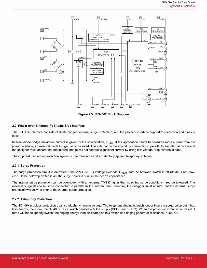
Figure 2.3. Si34062 Block Diagram
2.2 Power over Ethernet (PoE) Line-Side Interface
The PoE line interface consists of diode bridges, internal surge protection, and the protocol interface support for detection and classifi-cation.
Internal diode bridge maximum current is given by the specification, IRECT. If the application needs to consume more current from thepower interface, an external diode bridge has to be used. The external bridge should be connected in parallel to the internal bridge andthe designer must ensure that the internal bridge will not conduct significant current by using low-voltage-drop external diodes.
The chip features active protection against surge transients and accidentally applied telephony voltages.
2.2.1 Surge Protection
The surge protection circuit is activated if the VPOS-VNEG voltage exceeds TPROT and the hotswap switch is off (dc-dc is not pow-ered). If the hotswap switch is on, the surge power is sunk in the dcdc’s capacitance.
The internal surge protection can be overridden with an external TVS if higher than specified surge conditions need be tolerated. Theexternal surge device must be connected in parallel to the internal one; therefore, the designer must ensure that the external surgeprotection will activate prior to the internal surge protection.
2.2.2 Telephony Protection
The Si3406x provides protection against telephony ringing voltage. The telephony ringing is much longer than the surge pulse but it hasless energy, therefore, the Si3406x has a switch parallel with the supply (VPOS and VNEG). When the protection circuit is activated, itturns ON the telephony switch; the ringing energy then dissipates on this switch and ringing generator resistance (> 400 Ω).
Si3406x Family Data SheetSystem Overview
silabs.com | Building a more connected world. Preliminary Rev. 0.5 | 5

2.2.3 Detection and Classification
When si3406x is connected to the Ethernet cable it has to provide a characteristic resistance (~25 kΩ) to the PSE in a given voltagerange (2.7–10.1 V). This is called detection. After thePSE detects the PD, the PSE increases the voltage above the classificationthreshold 14.5 V. Then, the PD provides the classification current to inform the PSE about its required power class (Class 1, 2, 3, or 4).Type 1 PSEs cannot provide enough power for a Class4 PD. Type 2 PSEs have additional voltage steps before switching on the PD.After an initial classification voltage pulse, the Type 2 PSE reduces the voltage below the mark threshold level (10 V) then raises it upagain to the Class event range. Last, before switching ON the DCDC it reduces the voltage again. This sequence is recognized by thesi3406x and its pull down its nT2P pin to inform the application about the higher available power; otherwise, the application will need tooperate in a reduced power consumption state (Type 1) if the PSE is incapable of delivering Class 4 power.
Figure 2.4. Powered Device Voltages
2.3 Hotswap Switch
The internal hotswap switch (HSSW) is turned on (conducting) when the PoE interface voltage goes above VUVLO_R. It provides limitedinrush current until the dcdc side capacitor is charged. The hotswap switch turns off (open) if voltage on the HSSW switch (HSO-VNEG)is greater than VHSSW_OFF.
In overload, the hotswap switch goes into current-limiting mode with a current limit of IOVL. It will turn back ON after TWAITHSSW elap-ses and the dc-dc input capacitor is recharged, meaning the HSO-VNEG voltage is less than VHSSW_ON.
The hotswap switch (if it is in the on state and conducting) can detect if the current is lower than IMPSth. In this case, the chip turns onMPS pulse generation, which ensures that the PSE will not disconnect.
With the Si34061, an external hotswap switch can be used to improve efficiency and reduce thermal stress in high current applications.For Class 3 applications, using an external hotswap switch is recommended; for Class 4, it is mandatory because the internal hotswapswitch otherwise generates significant heat. When an external hotswap switch is used, intelligent switch control ensures that inrush cur-rent limiting and automatic MPS request of the internal switch are still supported.
Si3406x Family Data SheetSystem Overview
silabs.com | Building a more connected world. Preliminary Rev. 0.5 | 6

2.4 HSSW State Machine
The HSSW operates as simple 4-state state machine:
Figure 2.5. Hotswap Switch 4-State Machine
Note: Internal signal names are shown in this Figure, not to be confused with external pin names. For the below discussion, ILOAD isthe switch current, and VHSSW is the voltage drop of the switch. In other words, VHSSW = HSO – VNEG. All the voltage, current andtime limits of the above diagram are typical values.
OFF State
HSSW turn-on is controlled by UVLO, the undervoltage lockout feature. When UVLO is engaged, the HSSW is OFF. In this state, theHSSW is in idle mode, VNEG and HSO pins are disconnected. In normal operation, a complete detect/classification procedure pre-cedes the HSSW turn-on, and the control of this sequence is implemented in the state machine logic of the chip.
INRUSH State
After the controller enables the HSSW, the block starts operation in the INRUSH state. In this state the switch itself is not directly turnedon, but operating in a closed-loop current limit mode to avoid high current peaks during the charging of the primary bypass cap of the dcto dc converter.
If the VHSSW voltage drops below 380 mV (meaning the bypass cap is 99% charged), the HSSW will change state to ON either inType1 classification immediately, or in Type2 classification if the HSSW has been in the INRUSH state for at least 80 ms.
ON State
In ON state, the HSSW switch is directly turned on. The HSSW circuit continuously monitors VHSSW. HSSW will change to OVERLOADstate if VHSSW voltage increases over 3.6 V for at least 140 µs.
OVERLOAD State
In OVERLOAD state the HSSW operates in closed-loop low current limit mode. If the VHSSW voltage drops below 360 mV again, andthe HSSW has been in the OVERLOAD state for at least 80 ms, the HSSW will change back to the ON state.
2.4.1 External HSSW FET Driver
An external HSSW FET may be used to improve thermal operation of an Si34061 at very high power loading levels (the top end ofClass 4).
With the Si34061, the chip automatically detects if the EXTHSW pin is connected to VNEG or to a FET gate at startup. If the externalhotswap FET driver will not be used, the EXTHSW pin must be tied to VNEG.
For further information on using an external HSSW FET, please refer to "AN1130: Using the Si3406/Si34061/Si34062 PoE+ and Si3404PoE PD Controller In Isolated and Non-Isolated Designs".
Si3406x Family Data SheetSystem Overview
silabs.com | Building a more connected world. Preliminary Rev. 0.5 | 7
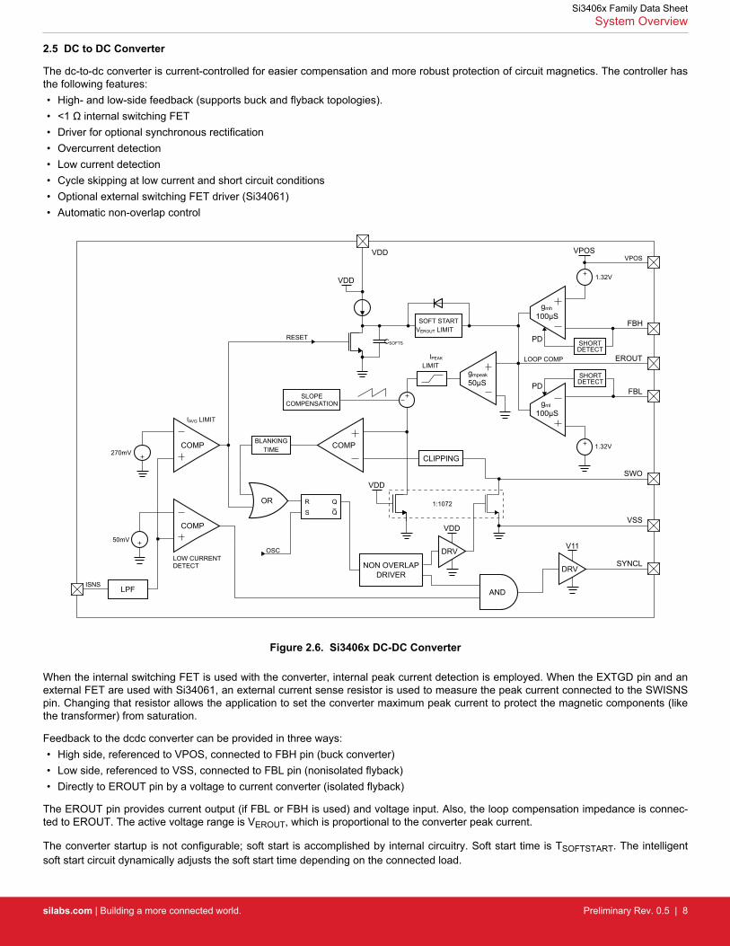
2.5 DC to DC Converter
The dc-to-dc converter is current-controlled for easier compensation and more robust protection of circuit magnetics. The controller hasthe following features:• High- and low-side feedback (supports buck and flyback topologies).• <1 Ω internal switching FET• Driver for optional synchronous rectification• Overcurrent detection• Low current detection• Cycle skipping at low current and short circuit conditions• Optional external switching FET driver (Si34061)• Automatic non-overlap control
SWO
EROUT
FBL
FBH
V11
SYNCLDRV
1.32V
gmh
100µS
gml
100µS
gmpeak
50µS
1.32V
IPEAK
LIMIT
VDD
DRV
NON OVERLAPDRIVER
1:1072
COMP
CLIPPING
BLANKINGTIME
VDD
R QQ
COMP270mV
50mV
COMP
LPFISNS
OSC
CSOFTS
SOFT STARTVEROUT LIMIT
RESET
LOOP COMP
VPOS
IAVG LIMIT
LOW CURRENTDETECT
PD
VDD
OR
AND
SLOPECOMPENSATION
S
SHORTDETECT
PD SHORTDETECT
VSS
VPOS
VDD
Figure 2.6. Si3406x DC-DC Converter
When the internal switching FET is used with the converter, internal peak current detection is employed. When the EXTGD pin and anexternal FET are used with Si34061, an external current sense resistor is used to measure the peak current connected to the SWISNSpin. Changing that resistor allows the application to set the converter maximum peak current to protect the magnetic components (likethe transformer) from saturation.
Feedback to the dcdc converter can be provided in three ways:• High side, referenced to VPOS, connected to FBH pin (buck converter)• Low side, referenced to VSS, connected to FBL pin (nonisolated flyback)• Directly to EROUT pin by a voltage to current converter (isolated flyback)
The EROUT pin provides current output (if FBL or FBH is used) and voltage input. Also, the loop compensation impedance is connec-ted to EROUT. The active voltage range is VEROUT, which is proportional to the converter peak current.
The converter startup is not configurable; soft start is accomplished by internal circuitry. Soft start time is TSOFTSTART. The intelligentsoft start circuit dynamically adjusts the soft start time depending on the connected load.
Si3406x Family Data SheetSystem Overview
silabs.com | Building a more connected world. Preliminary Rev. 0.5 | 8

2.5.1 Average Current Sensing, Overcurrent, and Low-Current Detection
The application average current is sensed by an external resistor (RSENSE) connected between VSS and ISNS. Overcurrent is detectedand triggered when the voltage on the sense resistor exceeds VISNS_OVC. Sizing the resistor allows the designer to set the overcurrentlimit according to application needs. When overcurrent is triggered, the dcdc controller goes into reset until the overcurrent resolves.When the overcurrent is no longer present, the controller starts up again with softstart.
This external sense resistor is also used to detect a low current situation. When the voltage on the sense resistor goes below VISNS_LC,the dcdc controller disables the sync FET and the external hotswap switch, allowing very low current consumption—the internal hots-wap switch then measures the chip current internally. If the average current is lower than the PoE maintain power signature (MPS) limit,and if automatic sleep mode is enabled, the chip turns on the MPS generation. See the sleep mode section for further detail.
2.5.2 Sync FET Driver
With the Si3406x family, an optional synchronous rectifying FET may be used in place of an output rectifier diode for improved powerconversion efficiency.
A gate driver is provided for this purpose. The synchronous rectifying FET driver is enabled by default in Si3406x configurations, but, ifa synchronous FET is not used in the design, the SYNCL pin must not be connected (do not connect SYNCL to any power or groundrail). The synchronous rectifying FET driver is disabled only when the dcdc converter measures low average current (meaning lowerthan VISNS_LC on ISNS). This ensures low sleep mode current consumption.
2.6 External HSSW FET Driver
An external HSSW FET may be used to improve thermal operation of an Si34061 at very high power loading levels (the top end ofClass 4).
With the Si34061, the chip automatically detects if the EXTHSW pin is connected to VNEG or to a FET gate at startup. If the externalhotswap FET driver will not be used, the EXTHSW pin must be tied to VNEG.
For further information on using an external HSSW FET, please refer to "AN1130: Using the Si3406/Si34061/Si34062 PoE+ and Si3404PoE PD Controller In Isolated and Non-Isolated Designs".
2.7 Tunable Oscillator
The dcdc frequency can be fixed to 250 kHz or tunable by an external resistor.
The tuning resistor must be connected between the RFREQ pin and VPOS. If RFREQ is shorted to VPOS, the fixed frequency oscillatorwill provide the clock, FOSCINT, to the dcdc converter; otherwise, the resistor will determine the frequency as shown in the curve below.
Figure 2.7. RFREQ Frequency Selector Diagram
Si3406x Family Data SheetSystem Overview
silabs.com | Building a more connected world. Preliminary Rev. 0.5 | 9

2.8 Regulators
The chip provides a 5 V output to power LEDs or optocouplers. This is a closed-loop regulator, which ensures accurate output voltage.The 5 V regulator is supplied by an internal 11 V open loop regulator, which also provides power for the external FET gate drivers. The11 V regulator is supplied by a coarse regulator, which is also open-loop. With the Si34061 and Si34062, the VT15 pin can be used tosupply this regulator from an optional auxiliary transformer winding. The advantage of doing so is additional power saving since theexternal FET drivers’ current is not generated from the PoE 50 V but, rather, from a transformer-provided 12–16 V. The applicationmust be designed to ensure that the absolute maximum rating voltage for the VT15 pin is not exceeded.
2.9 Sleep Mode
The Si3406, Si34061, and Si34062 have automatic (consumption-based) and non-automatic sleep modes. When SLEEPb is tied toground, the automatic sleep mode is enabled, meaning that if the current consumption is lower than IMPSth, the chip will automaticallygenerate MPS pulses to the PSE. If SLEEPb is tied to VDD, then it will not generate MPS pulses, and the PSE will disconnect if totalapplication current consumption drops below 5–10 mA.
For non-automatic sleep mode, tie SLEEPb high at initial startup (right after the hotswap switch turns on). The chip turns OFF automaticmode, but pulling SLEEPb low will force MPS generation as long as the pin is held low. Using this mode, the designer can control MPSgeneration.
2.10 Extended Sleep Mode
In the Si34062, an extended sleep mode is available which includes LED, WAKE, and MODE pin support. The LED pin drives a lightemitting diode to (for example) illuminate a button on the primary side of the application. The WAKE pin triggers wakeup, and theMODE button controls if MPS generation is enabled in sleep. In the Si34062 case, nSLEEP is used to initiate sleep.
The sleep mode is initiated by a negative transition on nSLEEP. It is latched at that negative transition event together with MODE, sotheir status is kept until wakeup even if the input changes on these pins due to the secondary side losing power. MPS generation isenabled if MODE = 0 at the nSLEEP transition. The following figure shows the Si34062 sleep mode behavior.
Chip Sleep, DCDC Off
Mode?
Chip Awake,DCDC Runs
WAK
E Po
s. E
dge NSLEEP Neg.Edge
Low
High
Turn MPS Generation ON
Figure 2.8. Si34062 Extended Sleep Mode Behavior
Refer to Figure 3.3 Si34062 ISO Flyback Application Diagram on page 13, which shows shows the connectivity for the Si34062 withthe extended sleep mode.
Si3406x Family Data SheetSystem Overview
silabs.com | Building a more connected world. Preliminary Rev. 0.5 | 10

2.11 External Wall Support
The Si3406x supports using a wide voltage range of external wall adapters as a primary or secondary supply. For details on optionsand supported modes of adapter connection, please refer to "AN1130: Using the Si3406/Si34061/Si34062 PoE+ and Si3404 PoE PDController In Isolated and Non-Isolated Designs".
ASUP VPOS
SWO
C
RISNS
VSS
ISNS
HSO
RASUPVAUX
100k
Si34061
VNEGVNEG
VPOS
HSO
HSO
From PSE
12V-57V
Figure 2.9. Example Auxiliary Wall Adapter Connection
Si3406x Family Data SheetSystem Overview
silabs.com | Building a more connected world. Preliminary Rev. 0.5 | 11

3. Application Examples
The following diagrams demonstrate the ease of use and straightforward BOM of the Si3406x Powered Device ICs. Detailed referencedesigns are available in Evaluation KIT User Guides. Also refer to "AN1130: Using the Si3406/Si34061/Si34062 PoE+ and Si3404 PoEPD Controller In Isolated and Non-Isolated Designs".
RFREQ
RFREQVPOS VSS
CIN
VPOS
RDETRDET
CT1
CT2
SP1
SP2
RCLASSRCLASS
EROUT
FBL
SYNCL
SWO
VDDVNEG
Si3406
VNEG
CDET
VSS VSS VSS
VSS
RCOMP
CCOMP
COUT
R1
R2
syncFET
VOUT
C
RSENSE
ISNSHSO
VSS
ct1
ct2
sp1
sp2
Figure 3.1. Si3406 Non-ISO Flyback Application Diagram
RFREQ
RFREQVPOS VSS
CIN
VPOS
RDETRDET
CT1
CT2
SP1
SP2
RCLASSRCLASS
EROUT
VDD
SYNCL
SWO
VDD
VNEG
Si34061
VNEG
CDET
VSS
VSS
RCOMP1
CCOMP1
COUTsyncFET
VOUT
C
VIN
VINEXTHSW HSO ISNS
RSENSE
VSS
VT15
VSS GNDI
GNDI
EXTHSW
VSS
RCOMP2 CCOMP2
TLV431R2
R1
GNDI
GNDI
BIAS
VSS
*GNDI = ISOLATED GROUND
Figure 3.2. Si34061 ISO Flyback Application Diagram
Si3406x Family Data SheetApplication Examples
silabs.com | Building a more connected world. Preliminary Rev. 0.5 | 12
RFREQ
RFREQVPOS VSS
CIN
VPOS
RDETRDET
CT1CT2SP1SP2
RCLASSRCLASS
EROUT
VDD
SYNCL
SWO
VNEG
Si34062
VNEG
CDET
VSS
VSS
RCOMP1
CCOMP1
COUTsyncFET
VOUT
C
HSO ISNS
RSENSE
VSS
VT15
VSS GNDI
GNDIVSS
RCOMP2 CCOMP2
TLV431R2
R1
GNDI
GNDI
VSS GNDI
VSS GNDI
VSS GNDI
VDD
VDD
nsleep
VDD
'wake'
wake
mode
VOUT
SLEEP
GNDI
VOUT
VOUT
WAKEMODENSLEEP
LED
BIAS
nsleep
wakemode
VSS
VDD
*GNDI = ISOLATED GROUND
ct1
ct2
sp1
sp2
LED
Figure 3.3. Si34062 ISO Flyback Application Diagram
Si3406x Family Data SheetApplication Examples
silabs.com | Building a more connected world. Preliminary Rev. 0.5 | 13
4. Electrical Specifications
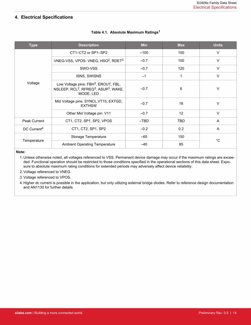
Table 4.1. Absolute Maximum Ratings1
Type Description Min Max Units
Voltage
CT1–CT2 or SP1–SP2 –100 100 V
VNEG-VSS, VPOS- VNEG, HSO2, RDET3 –0.7 100 V
SWO-VSS –0.7 120 V
ISNS, SWISNS –1 1 V
Low Voltage pins: FBH3, EROUT, FBL,NSLEEP, RCL2, RFREQ3, ASUP3, WAKE,
MODE, LED–0.7 6 V
Mid Voltage pins: SYNCL,VT15, EXTGD,EXTHSW –0.7 18 V
Other Mid Voltage pin: V11 –0.7 12 V
Peak Current CT1, CT2, SP1, SP2, VPOS –TBD TBD A
DC Current4 CT1, CT2, SP1, SP2 –0.2 0.2 A
TemperatureStorage Temperature –65 150
°CAmbient Operating Temperature –40 85
Note:1. Unless otherwise noted, all voltages referenced to VSS. Permanent device damage may occur if the maximum ratings are excee-
ded. Functional operation should be restricted to those conditions specified in the operational sections of this data sheet. Expo-sure to absolute maximum rating conditions for extended periods may adversely affect device reliability.
2. Voltage referenced to VNEG.3. Voltage referenced to VPOS.4. Higher dc current is possible in the application, but only utilizing external bridge diodes. Refer to reference design documentation
and AN1130 for further details.
Si3406x Family Data SheetElectrical Specifications
silabs.com | Building a more connected world. Preliminary Rev. 0.5 | 14

Table 4.2. Recommended Operating Conditions
Symbol Parameter (Condition) Min Typ Max Unit
VPORT |CT1 – CT2| or |SP1 – SP2| 2.7 — 57 V
VHV_OPVNEG-VSS, VNEG-HSO, VPOS-
VSS 2.7 — 57 V
VLV_OPVPOS referred low voltage pins:
RFREQ, RDET, FBH –5.5 — 0 V
VLV_OP
VSS referred low voltage pins: VDD,FBL, EROUT, ASUP, nSLEEP,
nT2P, ASUP, WAKE, MODE, LED0 — 5.5 V
VOH_DIG VOH of ASUP and nT2P relative toVSS.
3 — — V
VISNS_OPVSS referred current sensing pins:
ISNS, SWISNS –0.5 — 0.5 V
VLV_OPVNEG referred low voltage pins:
RCL 0 — 5.5 V
VMV_OPVSS referred medium voltage pins
SYNCL, EXTGD, EXTHSW 0 — 13 V
VMV_VT15VSS referred medium voltage pin
VT151 12 14.5 16.5 V
IRECTOn chip rectifier current on CT1,CT2, SP1, SP2—steady state2 — — 176 mA
VRECTOn chip rectifier voltage @ 200 mA,
2 diodes — 1.8 — V
IRECT_PKPeak rectifier current Max 75 ms 5%
Duty Cycle3 — — 231 mA
IAVGAllowable continuous current on
SWO, VSS, HSO, VNEG — — 600 mA
IPEAKPeak current on SWO, VSS, HSO,VNEG Max 75 ms 5% Duty Cycle — — 683 mA
Note:1. VMV_VT15 is relevant for Si34061 and Si34062 only when an external auxiliary winding from the primary side of the transformer is
being used to improve power conversion efficiency. This can be left undriven, in which case an internal regulator will be used.2. For Class 3 and above operation, use external diode bridge rectifiers to bypass the internal input diode bridge rectifiers.3. The IEEE 802.3at specification allows for higher peak current for transients.
Si3406x Family Data SheetElectrical Specifications
silabs.com | Building a more connected world. Preliminary Rev. 0.5 | 15

Table 4.3. Electrical Characteristics
Symbol Parameter (Condition) Min Typ Max Unit
PoE PROTOCOL
Detection
VDET Detection Voltage (at VPORT) 2.7 — 10.1 V
Classification
VRESET Classification Reset (at VPORT) 0 — 2.81 V
VCLASS Classification Voltage (at VPORT) 14.5 — 20.5 V
IPortCLASS
Class 0 (RCLASS > 681 Ω) 0 — 4 mA
Class 1 (RCLASS = 140 Ω @ 1%) 9 — 12 mA
Class 2 (RCLASS = 75 Ω @ 1%) 17 — 20 mA
Class 3 (RCLASS = 48.7 Ω @ 1%) 26 — 30 mA
Class 4 (RCLASS = 33.2 Ω @ 1 %) 36 — 44 mA
Type 2 Classification
VMARK Mark event voltage (at VPORT) 6.9 — 10.1 V
IMARK Mark event current 0.25 TBD 4 mA
Power On and UVLO
VUVLO_R Hotswap closed and converter on — 37 — V
VUVLO_F Hotswap open and converter off — 32 — V
Thermal Characteristics
Tshd Thermal shutdown — 160 — °C
THYST Thermal shutdown hysteresis — 20 — °C
On-Chip Transient Voltage Suppression/Protection
TPROTTVS protection activation voltage
(VPOS-VNEG) 100 — — V
Hotswap Switch
Iinrush Inrush current 100 170 200 mA
IMAXHSSWMaximum continuous operating cur-
rent — — 600 mA
VHSSW_ON Switch ON voltage — 380 — mV
VHSSW_OFFSwitch OFF voltage, HSSW goes to
overload cycle — 3.5 — V
IOVLSwitch current limit in OVERLOAD
State 8.7 10.5 12.4 mA
IMPSthMPS signal request current level
threshold 14 20 26 mA
IEXT_DRVExternal hotswap driver peak current
on EXTHSW pin — — 10 mA
Si3406x Family Data SheetElectrical Specifications
silabs.com | Building a more connected world. Preliminary Rev. 0.5 | 16

Symbol Parameter (Condition) Min Typ Max Unit
VEXT_DRVExternal hotswap driver voltage on
EXTHSW pin 9 11 — V
TWAITHSSWWait time in OVERLOAD and type 2
inrush 80 96 116 ms
RONHSSW Internal hotswap drain-source resist-ance while ON
0.65 1.5 2.9 Ω
DC-DC
ISWOPEAKPeak current limit of internal FET
(SWO pin) 2.1 — 2.7 A
VEXTGDExternal FET driver voltage (EXTGD
pin) 9 11 13 V
IEXTGDExternal FET driver peak current
(EXTGD pin) — — 500 mA
FOSCINT Using internal Oscillator — 250 — kHz
FOSCEXTUsing external Oscillator, tunable on
pin RFREQ 100 — 500 kHz
DUC Output duty cycle of PWM — TBD 75 %
VDCDCUVLODCDC UVLO level (Minimum adapt-
er voltage) 10.2 10.7 11.3 V
VFBREF
FBH (referenced to VPOS) and FBL(referenced to VSS) reference volt-
age— 1.32 — V
VEROUTOperating voltage range of error in-
put 1 — 4 V
VISNS_OVCOvercurrent limit voltage on ISNS
(ref. to VSS) — –270 — mV
VISNS_LCLow current limit voltage on ISNS
(ref. to VSS) — –30 — mV
VSWISNSMAX External FET current sense — 240 — mV
TSOFTSTART Startup time — 4 — ms
RONDCDC Internal DCDC switching FET drain-source resistance while ON
— 0.9 1.2 Ω
Regulators
VT15 Override internal regulator withtransformer winding 13 — 16.5 V
VDD High accuracy 5 V 4.85 5.1 5.46 V
VDDILIM DC current limit of VDD 9.7 11.2 12.9 mA
CREG Filter capacitor on VDD and V11 — 100 — nF
IMAXLEDLED pin max current, reduces
VDDILIM— 5 — mA
IMAXDODigital output max current (NT2P),
reduces VDDILIM2 2.5 — mA
Power Dissipation
Si3406x Family Data SheetElectrical Specifications
silabs.com | Building a more connected world. Preliminary Rev. 0.5 | 17
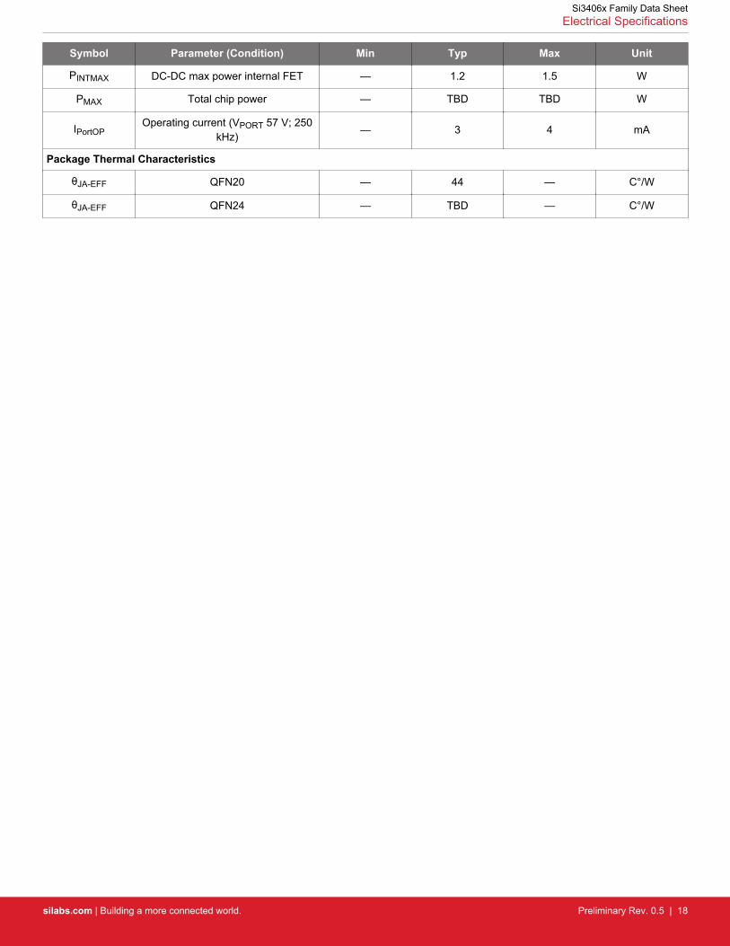
Symbol Parameter (Condition) Min Typ Max Unit
PINTMAX DC-DC max power internal FET — 1.2 1.5 W
PMAX Total chip power — TBD TBD W
IPortOPOperating current (VPORT 57 V; 250
kHz)— 3 4 mA
Package Thermal Characteristics
θJA-EFF QFN20 — 44 — C°/W
θJA-EFF QFN24 — TBD — C°/W
Si3406x Family Data SheetElectrical Specifications
silabs.com | Building a more connected world. Preliminary Rev. 0.5 | 18

5. Pin Descriptions
Si3406 Pinout(Top View)
Si34061 Pinout(Top View)
Si34062 Pinout(Top View)
FBH
EROUT
FBL
VDD
nSLE
EP
RD
ET
SP
2
RC
L
RFR
EQ
SP1
HS
O
VPOS
CT2
CT1
VNEG(ePad)
ISN
S
VS
S
SY
NC
L
nT2P
V11
SW
O
5 6 7 8 9 10
16 1517181920
1
2
3
4 11
12
13
14
ISNS
EROUT
FBL
VDD
nSLE
EP
RD
ET
SP
2
RC
L
RFR
EQ
SP1
HS
O
VPOS
CT2
CT1VNEG(ePad)
SW
ISN
S
VS
S
SY
NC
L
V11
SW
O
7 8 9 10
20 1921222324
2
3
4
5
13
14
15
16
11 12
1
6
EXTHSW
ASUP
17
18
nT2P
VT15
EX
TGD
FBH
EROUT
FBL
VDD
nSLE
EP
RD
ET
SP
2
RC
L
RFR
EQ
SP1
HS
O
VPOS
CT2
CT1VNEG(ePad)
ISN
S
VS
S
SY
NC
L
V11
SW
O
7 8 9 10
20 1921222324
2
3
4
5
13
14
15
16
11 12
1
6
LED
WAKE
17
18
nT2P
VT15
MO
DE
Table 5.1. Pin Descriptions
'06Pins
'061Pins
'062Pins
Name Ref Dir. Vrange Description
24 24 SWISNS VSS I 0–0.5 External FET peak current sense resistor voltage input
20 1 ISNS VSS I -0.5–0 Chip average current sense resistor input
1 1 FBH VPOS I 0–5 High side (VPOS referred) dcdc feedback (buck converter)
2 2 2 EROUT VSS IO 0–5 Error amplifier current output, compensation impedance input
3 3 3 FBL VSS I 0–5 Low side (ground referenced) dcdc feedback (flyback convert-er)
4 4 4 VDD VSS O 0–5 5V regulator output
5 LED VSS O 0–5 Output to drive sleep LED
5 EXTHSW VNEG O 0–11 External hotswap switch drive
6 WAKE VSS I 0–5 Wakeup from sleep mode
6 ASUP VSS I 0–5 AUX auxiliary adapter present
5 7 7 nSLEEP VSS I 0–5 Sleep, with pull-up, driven by open drain
6 8 8 RDET VPOS IO 0–100 Detection resistor
7 9 9 HSO VNEG IO 0–100 Hotswap switch output
8 10 10 RCL VNEG IO 0–5 Classification resistor
9 11 11 RFREQ VPOS IO 0–5 Oscillator frequency tuning resistor, tie to VPOS to select de-fault freq
10 12 12 SP2 SP1 I 0 - 100 High-voltage supply input from spare pair; polarity-insensitive
11 13 13 SP1 SP2 I 0–100 High-voltage supply input from spare pair; polarity-insensitive
12 14 14 VPOS — IO 0–100 Rectified high-voltage supply positive rail
13 15 15 CT2 CT1 I 0–100 High-voltage supply input from main pair; polarity-insensitive
14 16 16 CT1 CT2 I 0 - 100 High-voltage supply input from main pair; polarity-insensitive
Si3406x Family Data SheetPin Descriptions
silabs.com | Building a more connected world. Preliminary Rev. 0.5 | 19

'06Pins
'061Pins
'062Pins
Name Ref Dir. Vrange Description
15 17 17 nT2P VSS O 0–5 Type II classification was successful
18 18 VT15 VSS I 0–16.5 Dcdc transformer bias winding input
16 19 19 SYNCL VSS O 0–11 Gate driver for synchronous rectification FET
17 20 20 V11 VSS IO 0–11 11 V regulator output for filter cap.
21 EXTGD VSS O 0–11 External FET gate drive.When internal switching FET is in use, tie to VSS.
21 MODE VSS I 0–5 Controls MPS and LED switch behavior
18 22 22 SWO VSS O 0–120 Internal dcdc switch output (NMOS drain)
19 23 23 VSS — IO 0 Dcdc converter primary ground
ePad ePad ePad VNEG — IO 0 Rectified high voltage supply ground
Si3406x Family Data SheetPin Descriptions
silabs.com | Building a more connected world. Preliminary Rev. 0.5 | 20

5.1 Detailed Pin Descriptions
Table 5.2. Circuit Equivalent and Description of Die Pads
Pin Name Detailed Description Circuit Detail
SWISNSExternal dcdc switching FET peak current sense resistor input. The maxi-mum current of the switching FET should correspond to voltage VSWISN-
SMAX.
ISNSAverage current sense resistor input. The resistor value will set the maxi-mum allowed average current for the application. The overcurrent thresholdvoltage VISNS_OVC. Note that this pin voltage goes below VSS.
FBH High side dcdc feedback input. Need to be tied to VPOS when not used.See VFBREF.
EROUT
dcdc converter error output; current out, voltage sense. Loop compensatingimpedance should be connected here.
IEROUT = (VFBH – VFBREF) x 50 μA or
IEROUT = (VFBL – VFBREF) x 50 μA
FBLLow side dcdc feedback input. Need to be tied to VSS when not used. SeeVFBREF
Si3406x Family Data SheetPin Descriptions
silabs.com | Building a more connected world. Preliminary Rev. 0.5 | 21
Pin Name Detailed Description Circuit Detail
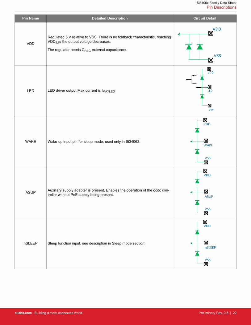
VDD
Regulated 5 V relative to VSS. There is no foldback characteristic, reachingVDDILIM the output voltage decreases.
The regulator needs CREG external capacitance.
LED LED driver output Max current is IMAXLED
WAKE Wake-up input pin for sleep mode, used only in Si34062.
ASUP Auxiliary supply adapter is present. Enables the operation of the dcdc con-troller without PoE supply being present.
nSLEEP Sleep function input, see description in Sleep mode section.
Si3406x Family Data SheetPin Descriptions
silabs.com | Building a more connected world. Preliminary Rev. 0.5 | 22
Pin Name Detailed Description Circuit Detail
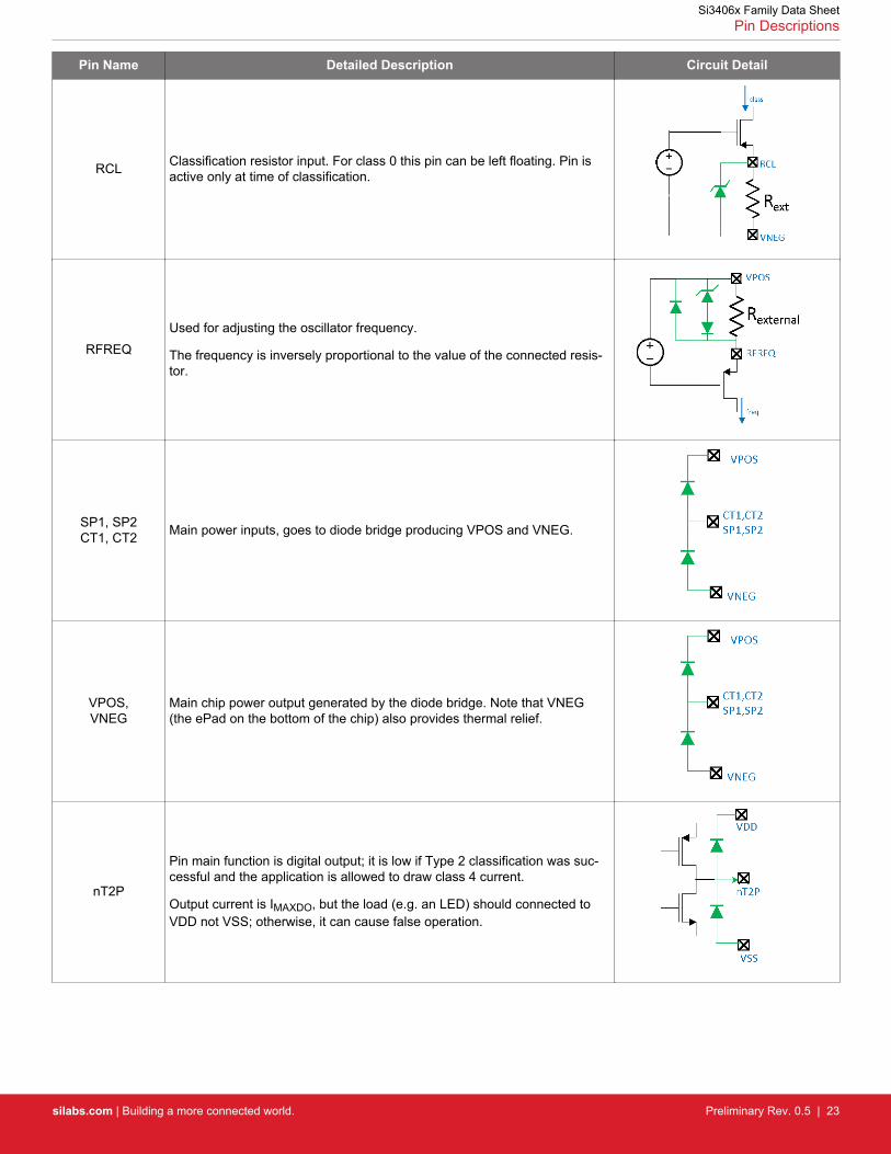
RCL Classification resistor input. For class 0 this pin can be left floating. Pin isactive only at time of classification.
RFREQUsed for adjusting the oscillator frequency.
The frequency is inversely proportional to the value of the connected resis-tor.
SP1, SP2CT1, CT2 Main power inputs, goes to diode bridge producing VPOS and VNEG.
VPOS,VNEG
Main chip power output generated by the diode bridge. Note that VNEG(the ePad on the bottom of the chip) also provides thermal relief.
nT2P
Pin main function is digital output; it is low if Type 2 classification was suc-cessful and the application is allowed to draw class 4 current.
Output current is IMAXDO, but the load (e.g. an LED) should connected toVDD not VSS; otherwise, it can cause false operation.
Si3406x Family Data SheetPin Descriptions
silabs.com | Building a more connected world. Preliminary Rev. 0.5 | 23
Pin Name Detailed Description Circuit Detail
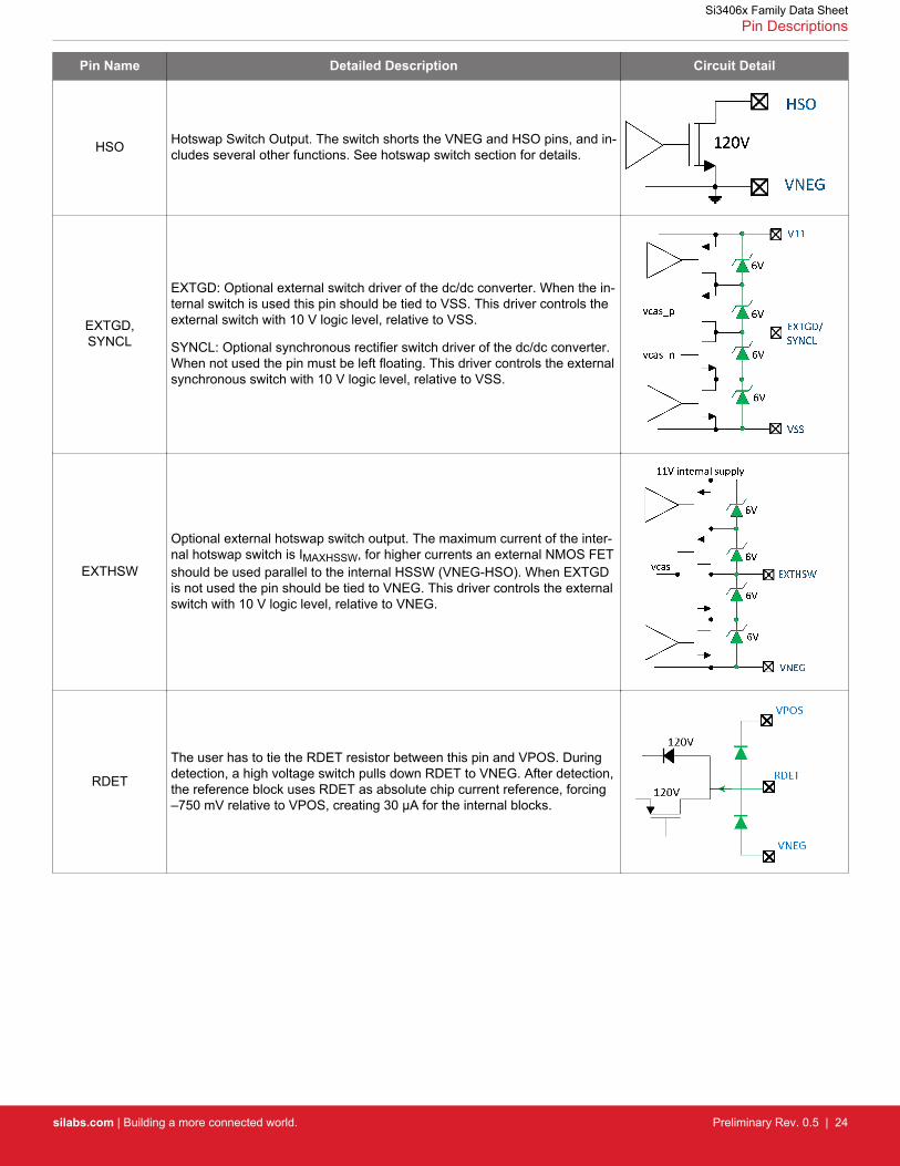
HSO Hotswap Switch Output. The switch shorts the VNEG and HSO pins, and in-cludes several other functions. See hotswap switch section for details.
EXTGD,SYNCL
EXTGD: Optional external switch driver of the dc/dc converter. When the in-ternal switch is used this pin should be tied to VSS. This driver controls theexternal switch with 10 V logic level, relative to VSS.
SYNCL: Optional synchronous rectifier switch driver of the dc/dc converter.When not used the pin must be left floating. This driver controls the externalsynchronous switch with 10 V logic level, relative to VSS.
EXTHSW
Optional external hotswap switch output. The maximum current of the inter-nal hotswap switch is IMAXHSSW, for higher currents an external NMOS FETshould be used parallel to the internal HSSW (VNEG-HSO). When EXTGDis not used the pin should be tied to VNEG. This driver controls the externalswitch with 10 V logic level, relative to VNEG.
RDET
The user has to tie the RDET resistor between this pin and VPOS. Duringdetection, a high voltage switch pulls down RDET to VNEG. After detection,the reference block uses RDET as absolute chip current reference, forcing–750 mV relative to VPOS, creating 30 µA for the internal blocks.
Si3406x Family Data SheetPin Descriptions
silabs.com | Building a more connected world. Preliminary Rev. 0.5 | 24

Pin Name Detailed Description Circuit Detail
VT15,V11
VT15 is input for an optional 15 V supply generated by an auxiliary trans-former bias winding. If the bias winding voltage is lower than VT15, the in-ternal 15 V coarse regulator will provide the current for the 11 V regulator.
The V11 pin is for filtering capacitor for the 11 V regulator. A capacitor ofvalue CREG is required.
MODE MPS mode control, used in Si34062.
SWO Dcdc converter switching transistor drain output, Vmax = 120 V.
VSS DC-DC converter ground.
Si3406x Family Data SheetPin Descriptions
silabs.com | Building a more connected world. Preliminary Rev. 0.5 | 25

6. Packaging
6.1 Package Outline: Si3406
The figure below illustrates the package details for the Si3406. The table lists the values for the dimensions shown in the illustration.
Figure 6.1. 20-Pin, QFN Package
Table 6.1. Package Diagram Dimensions
Dimension Min Nom Max
A 0.80 0.85 0.90
A1 0.00 0.02 0.05
b 0.25 0.30 0.35
D 5.00 BSC.
D2 2.60 2.70 2.80
e 0.80 BSC.
E 5.00 BSC.
E2 2.60 2.70 2.80
L 0.50 0.55 0.60
L1 0.00 — 0.10
aaa — — 0.10
bbb — — 0.10
ccc — — 0.08
ddd — — 0.10
Si3406x Family Data SheetPackaging
silabs.com | Building a more connected world. Preliminary Rev. 0.5 | 26

Dimension Min Nom Max
Note:1. All dimensions shown are in millimeters (mm) unless otherwise noted.2. Dimensioning and Tolerancing per ANSI Y14.5M-1994.3. This drawing conforms to the JEDEC Solid State Outline MO-220, Variation VHHB-1.
Si3406x Family Data SheetPackaging
silabs.com | Building a more connected world. Preliminary Rev. 0.5 | 27
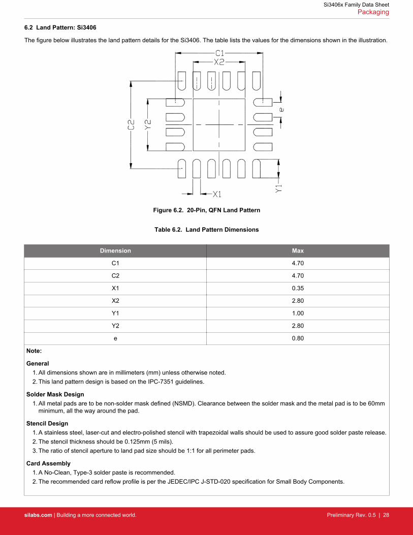
6.2 Land Pattern: Si3406
The figure below illustrates the land pattern details for the Si3406. The table lists the values for the dimensions shown in the illustration.
Figure 6.2. 20-Pin, QFN Land Pattern
Table 6.2. Land Pattern Dimensions
Dimension Max
C1 4.70
C2 4.70
X1 0.35
X2 2.80
Y1 1.00
Y2 2.80
e 0.80
Note:
General1. All dimensions shown are in millimeters (mm) unless otherwise noted.2. This land pattern design is based on the IPC-7351 guidelines.
Solder Mask Design1. All metal pads are to be non-solder mask defined (NSMD). Clearance between the solder mask and the metal pad is to be 60mm
minimum, all the way around the pad.
Stencil Design1. A stainless steel, laser-cut and electro-polished stencil with trapezoidal walls should be used to assure good solder paste release.2. The stencil thickness should be 0.125mm (5 mils).3. The ratio of stencil aperture to land pad size should be 1:1 for all perimeter pads.
Card Assembly1. A No-Clean, Type-3 solder paste is recommended.2. The recommended card reflow profile is per the JEDEC/IPC J-STD-020 specification for Small Body Components.
Si3406x Family Data SheetPackaging
silabs.com | Building a more connected world. Preliminary Rev. 0.5 | 28
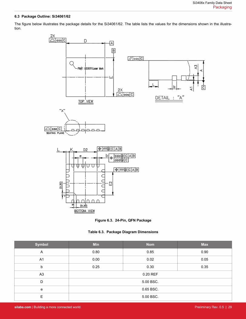
6.3 Package Outline: Si34061/62
The figure below illustrates the package details for the Si34061/62. The table lists the values for the dimensions shown in the illustra-tion.
Figure 6.3. 24-Pin, QFN Package
Table 6.3. Package Diagram Dimensions
Symbol Min Nom Max
A 0.80 0.85 0.90
A1 0.00 0.02 0.05
b 0.25 0.30 0.35
A3 0.20 REF
D 5.00 BSC.
e 0.65 BSC.
E 5.00 BSC.
Si3406x Family Data SheetPackaging
silabs.com | Building a more connected world. Preliminary Rev. 0.5 | 29

Symbol Min Nom Max
D2 2.90 3.00 3.10
E2 2.90 3.00 3.10
L 0.35 0.40 0.45
K 0.20 — —
aaa 0.15
bbb 0.10
ccc 0.10
ddd 0.05
eee 0.08
fff 0.10
Note:1. All dimensions shown are in millimeters (mm) unless otherwise noted.2. Dimensioning and Tolerancing per ANSI Y14.5M-1994.3. Recommended card reflow profile is per the JEDEC/IPC J-STD-020 specification for Small Body Components.
Si3406x Family Data SheetPackaging
silabs.com | Building a more connected world. Preliminary Rev. 0.5 | 30

6.4 Land Pattern: Si34061/62
The figure below illustrates the land pattern details for the Si34061/62. The table lists the values for the dimensions shown in the illus-tration.
Figure 6.4. 24-Pin, QFN Land Pattern
Table 6.4. Land Pattern Dimensions
Dimension mm
C1 4.90
C2 4.90
X1 0.35
X2 3.10
Y1 0.85
Y2 3.10
e 0.65
Note:
General1. All dimensions shown are in millimeters (mm) unless otherwise noted2. This land pattern design is based on the IPC-7351 guidelines
Solder Mask Design1. All metal pads are to be non-solder mask defined (NSMD). Clearance between the solder mask and the metal pad is to be 60 mm
minimum, all the way around the pad.
Stencil Design1. A stainless steel, laser-cut and electro-polished stencil with trapezoidal walls should be used to assure good solder paste release2. The stencil thickness should be 0.125 mm (5 mils)3. The ratio of stencil aperture to land pad size should be 1:1 for all perimeter pads.
Card Assembly1. A No-Clean, Type-3 solder paste is recommended.2. The recommended card reflow profile is per the JEDEC/IPC J-STD-020 specification for Small Body Components.
Si3406x Family Data SheetPackaging
silabs.com | Building a more connected world. Preliminary Rev. 0.5 | 31

7. Top Markings
7.1 Si3406 Top Marking
Figure 7.1. Si3406 Top Marking
Table 7.1. Si3406 Top Marking Explanation
Mark Method: Laser
Pin 1 Mark: Circle = 0.50 mm Diameter (Lower-Left Corner)
Font Size: 2.0 Point (28 mils)
Line 1 Mark Format: Device Part Number Si3406
Line 2 Mark Format: Device Type A = Device Revision A
G = Extended temperature range
M = QFN package
Line 3 Mark Format: TTTTTT Manufacturing Trace Code (assigned at assembly)
Line 4 Mark Format: YY = Year
WW = Work Week
Assembly Year
Assembly Week
Si3406x Family Data SheetTop Markings
silabs.com | Building a more connected world. Preliminary Rev. 0.5 | 32

7.2 Si34061 Top Marking
Figure 7.2. Si34061 Top Marking
Table 7.2. Si34061 Top Marking Explanation
Mark Method: Laser
Pin 1 Mark: Circle = 0.50 mm Diameter (Lower-Left Corner)
Font Size: 2.0 Point (28 mils)
Line 1 Mark Format: Device Part Number Si34061
Line 2 Mark Format: Device Type A = Device Revision A
G = Extended temperature range
M = QFN package
Line 3 Mark Format: TTTTTT Manufacturing Trace Code (assigned at assembly)
Line 4 Mark Format: YY = Year
WW = Work Week
Assembly Year
Assembly Week
Si3406x Family Data SheetTop Markings
silabs.com | Building a more connected world. Preliminary Rev. 0.5 | 33

7.3 Si34062 Top Marking
Figure 7.3. Si34062 Top Marking
Table 7.3. Si34062 Top Marking Explanation
Mark Method: Laser
Pin 1 Mark: Circle = 0.50 mm Diameter (Lower-Left Corner)
Font Size: 2.0 Point (28 mils)
Line 1 Mark Format: Device Part Number Si34062
Line 2 Mark Format: Device Type A = Device Revision A
G = Extended temperature range
M = QFN package
Line 3 Mark Format: TTTTTT Manufacturing Trace Code (assigned at assembly)
Line 4 Mark Format: YY = Year
WW = Work Week
Assembly Year
Assembly Week
Si3406x Family Data SheetTop Markings
silabs.com | Building a more connected world. Preliminary Rev. 0.5 | 34

8. Revision History
Revision 0.5
February, 2018
• Updated 2. System Overview and 3. Application Examples.• Added theory of operation and application content.
• Updated Table 4.1 Absolute Maximum Ratings1 on page 14, Table 4.2 Recommended Operating Conditions on page 15, and Table4.3 Electrical Characteristics on page 16.• Clarified multiple parameters.
• Added 5.1 Detailed Pin Descriptions.• Added 6. Packaging including outline and land pattern.
Revision 0.1
August, 2016
• Initial release.
Si3406x Family Data SheetRevision History
silabs.com | Building a more connected world. Preliminary Rev. 0.5 | 35

http://www.silabs.com
Silicon Laboratories Inc.400 West Cesar ChavezAustin, TX 78701USA
Smart. Connected. Energy-Friendly.
Productswww.silabs.com/products
Qualitywww.silabs.com/quality
Support and Communitycommunity.silabs.com
DisclaimerSilicon Labs intends to provide customers with the latest, accurate, and in-depth documentation of all peripherals and modules available for system and software implementers using or intending to use the Silicon Labs products. Characterization data, available modules and peripherals, memory sizes and memory addresses refer to each specific device, and "Typical" parameters provided can and do vary in different applications. Application examples described herein are for illustrative purposes only. Silicon Labs reserves the right to make changes without further notice and limitation to product information, specifications, and descriptions herein, and does not give warranties as to the accuracy or completeness of the included information. Silicon Labs shall have no liability for the consequences of use of the information supplied herein. This document does not imply or express copyright licenses granted hereunder to design or fabricate any integrated circuits. The products are not designed or authorized to be used within any Life Support System without the specific written consent of Silicon Labs. A "Life Support System" is any product or system intended to support or sustain life and/or health, which, if it fails, can be reasonably expected to result in significant personal injury or death. Silicon Labs products are not designed or authorized for military applications. Silicon Labs products shall under no circumstances be used in weapons of mass destruction including (but not limited to) nuclear, biological or chemical weapons, or missiles capable of delivering such weapons.
Trademark InformationSilicon Laboratories Inc.® , Silicon Laboratories®, Silicon Labs®, SiLabs® and the Silicon Labs logo®, Bluegiga®, Bluegiga Logo®, Clockbuilder®, CMEMS®, DSPLL®, EFM®, EFM32®, EFR, Ember®, Energy Micro, Energy Micro logo and combinations thereof, "the world’s most energy friendly microcontrollers", Ember®, EZLink®, EZRadio®, EZRadioPRO®, Gecko®, ISOmodem®, Micrium, Precision32®, ProSLIC®, Simplicity Studio®, SiPHY®, Telegesis, the Telegesis Logo®, USBXpress®, Zentri and others are trademarks or registered trademarks of Silicon Labs. ARM, CORTEX, Cortex-M3 and THUMB are trademarks or registered trademarks of ARM Holdings. Keil is a registered trademark of ARM Limited. All other products or brand names mentioned herein are trademarks of their respective holders.