shyamkumar thoziyoor, naveen muralimanohar, and norman p ... · shyamkumar thoziyoor, naveen...
TRANSCRIPT

CACTI 5.0
Shyamkumar Thoziyoor, Naveen Muralimanohar, and Norman P. Jouppi Advanced Architecture Laboratory HP Laboratories HPL-2007-167 October 19, 2007* cache, memory, area, power, access time
CACTI 5.0 is the latest major revision of the CACTI tool for modeling thedynamic power, access time, area, and leakage power of caches and other memories. CACTI 5.0 includes a number of major improvements over CACTI 4.0. First, as fabrication technologies enter the deep-submicron era, device andprocess parameter scaling has become non-linear. To better model this, the base technology modeling in CACTI 5.0 has been changed from simple linear scaling of the original CACTI 0.8 micron technology to models based on the ITRS roadmap. Second, embedded DRAM technology has become available fromsome vendors, and there is interest in 3D stacking of commodity DRAM withmodern chip multiprocessors. As another major enhancement, CACTI 5.0 adds modeling support of DRAM memories. Third, to support the significant technology modeling changes above and to enable fair comparisons of SRAMand DRAM technology, the CACTI code base has been extensively rewritten tobecome more modular. At the same time, various circuit assumptions have beenupdated to be more relevant to modern design practice. Finally, numerous bug fixes and small feature additions have been made. For example, the cache organization assumed by CACTI is now output graphically to assist users in understanding the output generated by CACTI.
* Internal Accession Date Only Approved for External Publication © Copyright 2007 Hewlett-Packard Development Company, L.P.

CACTI 5.0
Shyamkumar Thoziyoor, Naveen Muralimanohar, and Norman P. Jouppi
[email protected], [email protected], [email protected]
October 19, 2007
Abstract
CACTI 5.0 is the latest major revision of the CACTI tool for modeling the dynamic power, access
time, area, and leakage power of caches and other memories. CACTI 5.0 includes a number of major im-
provements over CACTI 4.0. First, as fabrication technologies enter the deep-submicron era, device and
process parameter scaling has become non-linear. To better model this, the base technology modeling in
CACTI 5.0 has been changed from simple linear scaling of the original CACTI 0.8 micron technology to
models based on the ITRS roadmap. Second, embedded DRAM technology has become available from
some vendors, and there is interest in 3D stacking of commodity DRAM with modern chip multiproces-
sors. As another major enhancement, CACTI 5.0 adds modeling support of DRAM memories. Third,
to support the significant technology modeling changes above and to enable fair comparisons of SRAM
and DRAM technology, the CACTI code base has been extensively rewritten to become more modular.
At the same time, various circuit assumptions have been updated to be more relevant to modern design
practice. Finally, numerous bug fixes and small feature additions have been made. For example, the
cache organization assumed by CACTI is now output graphically to assist users in understanding the
output generated by CACTI.
1

Contents
1 Introduction 4
2 Changes and Enhancements in Version 5.0 4
2.1 Organizational Changes . . . . . . . . . . . . . . . . . . . . . . . . . . . . . . . . . . . . . . . 42.2 Circuit and Sizing Changes . . . . . . . . . . . . . . . . . . . . . . . . . . . . . . . . . . . . . 42.3 Technology Changes . . . . . . . . . . . . . . . . . . . . . . . . . . . . . . . . . . . . . . . . . 52.4 DRAM Modeling . . . . . . . . . . . . . . . . . . . . . . . . . . . . . . . . . . . . . . . . . . . 62.5 Miscellaneous Changes . . . . . . . . . . . . . . . . . . . . . . . . . . . . . . . . . . . . . . . . 7
2.5.1 Optimization Function Change . . . . . . . . . . . . . . . . . . . . . . . . . . . . . . . 72.5.2 New Gate Area Model . . . . . . . . . . . . . . . . . . . . . . . . . . . . . . . . . . . . 72.5.3 Wire Model . . . . . . . . . . . . . . . . . . . . . . . . . . . . . . . . . . . . . . . . . . 72.5.4 ECC and Redundancy . . . . . . . . . . . . . . . . . . . . . . . . . . . . . . . . . . . . 72.5.5 Display Changes . . . . . . . . . . . . . . . . . . . . . . . . . . . . . . . . . . . . . . . 8
3 Data Array Organization 8
3.1 Mat Organization . . . . . . . . . . . . . . . . . . . . . . . . . . . . . . . . . . . . . . . . . . . 83.2 Routing to Mats . . . . . . . . . . . . . . . . . . . . . . . . . . . . . . . . . . . . . . . . . . . 113.3 Organizational Parameters of a Data Array . . . . . . . . . . . . . . . . . . . . . . . . . . . . 133.4 Comments about Organization of Data Array . . . . . . . . . . . . . . . . . . . . . . . . . . . 14
4 Circuit Models and Sizing 14
4.1 Wire Modeling . . . . . . . . . . . . . . . . . . . . . . . . . . . . . . . . . . . . . . . . . . . . 154.2 Sizing Philosophy . . . . . . . . . . . . . . . . . . . . . . . . . . . . . . . . . . . . . . . . . . . 164.3 Sizing of Mat Circuits . . . . . . . . . . . . . . . . . . . . . . . . . . . . . . . . . . . . . . . . 16
4.3.1 Predecoder and Decoder . . . . . . . . . . . . . . . . . . . . . . . . . . . . . . . . . . . 164.3.2 Bitline Peripheral Circuitry . . . . . . . . . . . . . . . . . . . . . . . . . . . . . . . . . 18
4.4 Sense Amplifier Circuit Model . . . . . . . . . . . . . . . . . . . . . . . . . . . . . . . . . . . . 214.5 Routing Networks . . . . . . . . . . . . . . . . . . . . . . . . . . . . . . . . . . . . . . . . . . 23
4.5.1 Array Edge to Bank Edge H-tree . . . . . . . . . . . . . . . . . . . . . . . . . . . . . . 234.5.2 Bank Edge to Mat H-tree . . . . . . . . . . . . . . . . . . . . . . . . . . . . . . . . . . 23
5 Area Modeling 24
5.1 Gate Area Model . . . . . . . . . . . . . . . . . . . . . . . . . . . . . . . . . . . . . . . . . . . 255.2 Area Model Equations . . . . . . . . . . . . . . . . . . . . . . . . . . . . . . . . . . . . . . . . 26
6 Delay Modeling 30
6.1 Access Time Equations . . . . . . . . . . . . . . . . . . . . . . . . . . . . . . . . . . . . . . . . 306.2 Random Cycle Time Equations . . . . . . . . . . . . . . . . . . . . . . . . . . . . . . . . . . . 31
7 Power Modeling 32
7.1 Calculation of Dynamic Energy . . . . . . . . . . . . . . . . . . . . . . . . . . . . . . . . . . . 327.1.1 Dynamic Energy Calculation Example for a CMOS Gate Stage . . . . . . . . . . . . . 327.1.2 Dynamic Energy Equations . . . . . . . . . . . . . . . . . . . . . . . . . . . . . . . . . 33
7.2 Calculation of Leakage Power . . . . . . . . . . . . . . . . . . . . . . . . . . . . . . . . . . . . 347.2.1 Leakage Power Calculation for CMOS gates . . . . . . . . . . . . . . . . . . . . . . . . 347.2.2 Leakage Power Equations . . . . . . . . . . . . . . . . . . . . . . . . . . . . . . . . . . 35
8 Technology Modeling 37
8.1 Devices . . . . . . . . . . . . . . . . . . . . . . . . . . . . . . . . . . . . . . . . . . . . . . . . 378.2 Wires . . . . . . . . . . . . . . . . . . . . . . . . . . . . . . . . . . . . . . . . . . . . . . . . . 398.3 Technology Exploration . . . . . . . . . . . . . . . . . . . . . . . . . . . . . . . . . . . . . . . 39
2

9 Embedded DRAM Modeling 40
9.1 Embedded DRAM Modeling Philosophy . . . . . . . . . . . . . . . . . . . . . . . . . . . . . . 409.1.1 Cell . . . . . . . . . . . . . . . . . . . . . . . . . . . . . . . . . . . . . . . . . . . . . . 409.1.2 Destructive Readout and Writeback . . . . . . . . . . . . . . . . . . . . . . . . . . . . 409.1.3 Sense amplifier Input Signal . . . . . . . . . . . . . . . . . . . . . . . . . . . . . . . . . 409.1.4 Refresh . . . . . . . . . . . . . . . . . . . . . . . . . . . . . . . . . . . . . . . . . . . . 419.1.5 Wordline Boosting . . . . . . . . . . . . . . . . . . . . . . . . . . . . . . . . . . . . . . 41
9.2 DRAM Array Organization and Layout . . . . . . . . . . . . . . . . . . . . . . . . . . . . . . 419.2.1 Bitline Multiplexing . . . . . . . . . . . . . . . . . . . . . . . . . . . . . . . . . . . . . 429.2.2 Reference Cells for VDD Precharge . . . . . . . . . . . . . . . . . . . . . . . . . . . . . 42
9.3 DRAM Timing Model . . . . . . . . . . . . . . . . . . . . . . . . . . . . . . . . . . . . . . . . 429.3.1 Bitline Model . . . . . . . . . . . . . . . . . . . . . . . . . . . . . . . . . . . . . . . . . 429.3.2 Multisubbank Interleave Cycle Time . . . . . . . . . . . . . . . . . . . . . . . . . . . . 439.3.3 Retention Time and Refresh Period . . . . . . . . . . . . . . . . . . . . . . . . . . . . 44
9.4 DRAM Power Model . . . . . . . . . . . . . . . . . . . . . . . . . . . . . . . . . . . . . . . . . 449.4.1 Refresh Power . . . . . . . . . . . . . . . . . . . . . . . . . . . . . . . . . . . . . . . . 45
9.5 DRAM Area Model . . . . . . . . . . . . . . . . . . . . . . . . . . . . . . . . . . . . . . . . . . 459.5.1 Area of Reference Cells . . . . . . . . . . . . . . . . . . . . . . . . . . . . . . . . . . . 459.5.2 Area of Refresh Circuitry . . . . . . . . . . . . . . . . . . . . . . . . . . . . . . . . . . 45
9.6 DRAM Technology Modeling . . . . . . . . . . . . . . . . . . . . . . . . . . . . . . . . . . . . 459.6.1 Cell Characteristics . . . . . . . . . . . . . . . . . . . . . . . . . . . . . . . . . . . . . 45
10 Cache Modeling 47
10.1 Organization . . . . . . . . . . . . . . . . . . . . . . . . . . . . . . . . . . . . . . . . . . . . . 4710.2 Delay Model . . . . . . . . . . . . . . . . . . . . . . . . . . . . . . . . . . . . . . . . . . . . . 4810.3 Area Model . . . . . . . . . . . . . . . . . . . . . . . . . . . . . . . . . . . . . . . . . . . . . . 4910.4 Power Model . . . . . . . . . . . . . . . . . . . . . . . . . . . . . . . . . . . . . . . . . . . . . 49
11 Quantitative Evaluation 49
11.1 Evaluation of New CACTI 5.0 Features . . . . . . . . . . . . . . . . . . . . . . . . . . . . . . 4911.1.1 Impact of New CACTI Solution Optimization . . . . . . . . . . . . . . . . . . . . . . . 4911.1.2 Impact of Device Technology . . . . . . . . . . . . . . . . . . . . . . . . . . . . . . . . 5011.1.3 Impact of Interconnect Technology . . . . . . . . . . . . . . . . . . . . . . . . . . . . . 5111.1.4 Impact of RAM Cell Technology . . . . . . . . . . . . . . . . . . . . . . . . . . . . . . 51
11.2 Version 4.2 vs Version 5.0 Comparisons . . . . . . . . . . . . . . . . . . . . . . . . . . . . . . 52
12 Validation 64
12.1 Sun SPARC 90 nm L2 cache . . . . . . . . . . . . . . . . . . . . . . . . . . . . . . . . . . . . 6412.2 Intel Xeon 65 nm L3 cache . . . . . . . . . . . . . . . . . . . . . . . . . . . . . . . . . . . . . 64
13 Future Work 71
14 Conclusions 71
A Additional CACTI Validation Results for 90 nm SPARC L2 72
B Additional CACTI Validation Results for 65 nm Xeon L3 77
3

1 Introduction
CACTI 5.0 is the latest major revision of the CACTI tool [1][2][3][4] for modeling the dynamic power, accesstime, area, and leakage power of caches and other memories. CACTI has become widely used by computerarchitects, both directly and indirectly through other tools such as Wattch.
CACTI 5.0 includes a number of major improvements over CACTI 4.0. First, as fabrication technogiesenter the deep-submicron era, device and process parameter scaling has become non-linear. To bettermodel this, the base technology modeling in CACTI 5.0 has been changed from simple linear scaling ofthe original 0.8 micron technology to models based on the ITRS roadmap. Second, embedded DRAMtechnology has become available from some vendors, and there is interest in 3D stacking of commodityDRAM with modern chip multiprocessors. As another major enhancement, CACTI 5.0 adds modelingsupport of DRAM memories. Third, to support the significant technology modeling changes above andto enable fair comparisons of SRAM and DRAM technology, the CACTI code base has been extensivelyrewritten to become more modular. At the same time, various circuit assumptions have been updated tobe more relevant to modern design practice. Finally, numerous bug fixes and small feature improvementshave been made. For example, the cache organization assumed by CACTI is now output graphically by theweb-based server, to assist users in understanding the output generated by CACTI.
The following section gives an overview of these changes, after which they are discussed in detail insubsequent sections.
2 Changes and Enhancements in Version 5.0
2.1 Organizational Changes
Earlier versions of CACTI (up to version 3.2) made use of a single row predecoder at the center of a memorybank with the row predecoded signals being driven to the subarrays for decoding. In version 4.0, thiscentralized decoding logic was implicitly replaced with distributed decoding logic. Using H-tree distribution,the address bits were transmitted to the distributed sinks where the decoding took place. However, becauseof some inconsistencies in the modeling, it was not clear at what granularity the distributed decoding tookplace - whether there was one sink per subarray or 2 or 4 subarrays. There were some other problems withthe CACTI code such as the following:
• The area model was not updated after version 3.2, so the impact on area of moving from centralizedto distributed decoding was not captured. Also, the leakage model did not account for the multi-ple distributed sinks. The impact of cache access type (normal/serial/fast) [4] on area was also notcaptured;
• Number of address bits routed to the subarrays was being computed incorrectly;
• Gate load seen by NAND gate in the 3-8 decode block was being computed incorrectly; and
• There were problems with the logic computing the degree of muxing at the tristate subarray outputdrivers.
In version 5.0, we resolve these issues, redefine and clarify what the organizational assumptions of memoryare and remove ambiguity from the modeling. Details about the organization of memory can be found inSection 3.
2.2 Circuit and Sizing Changes
Earlier versions of CACTI made use of row decoding logic with two stages - the first stage was composed of3-8 predecode blocks (composed of NAND3 gates) followed by a NOR decode gate and wordline driver. Thenumber of gates in the row decoding path was kept fixed and the gates were then sized using the methodof logical effort for an effective fanout of 3 per stage. In version 5.0, in addition to the row decoding logic,we also model the bitline mux decoding logic and the sense-amplifier mux decoding logic. We use the samecircuit structures to model all decoding logic and we base the modeling on the effort described in [5]. We
4
use the sizing heuristic described in [5] that has been shown to be good from an energy-delay perspective.With the new circuit structures and modeling that we use, the limit on maximum number of signals thatcan be decoded is increased from 4096 (in version 4.2) to 262144 (in version 5.0). While we do not expectthe number of signals that are decoded to be very high, extending the limit from 4096 helps with exploringarea/delay/power tradeoffs in a more thorough manner for large memories, especially for large DRAMs.Details of the modeling of decoding logic are described in Section 4.
There are certain problems with the modeling of the H-tree distribution network in version 4.2. Aninverter-driver is placed at branches of the address, datain and dataout H-tree. However, the dataout H-tree does not model tristate drivers. The output data bits may come from a few subarrays and so theaddress needs to be distributed to a few subarrays, however, dynamic power spent in transmitting addressis computed as if all the data comes from a single subarray. The leakage in the drivers of the datain H-treeis not modeled.
In verson 5.0, we model the H-tree distribution network more rigorously. For the dataout H-tree wemodel tristate buffers at each branch. For the address and datain H-trees, instead of assuming inverters atthe branches of the H-tree we assume the use of buffers that may be gated to allow or disallow the passage ofsignals and thereby control the dynamic power. We size these drivers based on the methodology describedin [5] which takes the resistance and capacitance of intermediate wires into account during sizing. We alsomodel the use of repeaters in the H-tree distribution network which are sized according to equations from[6].
2.3 Technology Changes
Earlier versions of CACTI relied on a complicated way of obtaining device data for the input technology-node. Computation of access/cycle time and dynamic power were based off device data of a 0.8-micronprocess that was scaled to the given technology-node using simple linear scaling principles. Leakage powercalculation, however, made use of Ioff (subthreshold leakage current) values that were based off device dataobtained through BSIM3 parameter extractions. In version 4.2, BSIM3 extraction was carried out for a fewselect technology nodes (130/100/70 nm); as a result leakage power estimation was available only for theseselect technology nodes.
There are several problems with the above approach of obtaining device data. Using two sets of parame-ters, one for computation of access/cycle time/dynamic power and another for leakage power, is a convolutedapproach and is hard to maintain. Also, the approach of basing device parameter values off a 0.8-micronprocess is not a good one because of several reasons. Device scaling has become quite non-linear in thedeep-submicron era. Device performance targets can no longer be achieved through simple linear scalingof device parameters. Moreover, it is well-known that physical gate-lengths (according to the ITRS, phys-ical gate-length is the final, as-etched length of the bottom of the gate electrode) have scaled much moreaggressively [7][8] than what would be projected by simple linear scaling from the 0.8 micron process.
In version 5.0, we adopt a simpler, more evolvable approach of obtaining device data. We use devicedata that the ITRS [7] uses to make its projections. The ITRS makes use of the MASTAR software tool(Model for Assessment of CMOS Technologies and Roadmaps) [9] for computation of device characteristicsof current and future technology nodes. Using MASTAR, device parameters may be obtained for differenttechnologies such as planar bulk, double gate and Silicon-On-Insulator. MASTAR includes device profileand result files of each year/technology-node for which the ITRS makes projections and we incorporate thedata from these files into CACTI. These device profiles are based off published industry process data andindustry-consensus targets set by historical trends and system drivers. While it is not necessary that thesedevice numbers match or would match process numbers of various vendors in an exact manner, they docome within the same ball-park as can be seen by looking at the Ion-Ioff cloud graphic within the MASTARsoftware which shows a scatter plot of various published vendor Ion-Ioff numbers and corresponding ITRSprojections. With this approach of using device data from the ITRS, it also becomes possible to incorporatedevice data corresponding to different device types that the ITRS defines such as high performance (HP),LSTP (Low Standby Power) and Low Operating Power (LOP). More details about the device data used inCACTI can be found in Section 8.
There are some problems with interconnect modeling of version 4.2 also. Version 4.2 utilizes 2 types ofwires in the delay model, ‘local’ and ‘global’. The local type is used for wordlines and bitlines, while the
5

global type is used for all other wires. The resistance per unit length and capacitance per unit length forthese two wire types are also calculated in a convoluted manner. For a given technology, the resistance perunit length of the local wire is calculated by assuming ideal scaling in all dimensions and using base data ofa 0.8-micron process. The base resistance per unit length for the 0.8-micron process is itself calculated byassuming copper wires in the base 0.8-micron process and readjusting the sheet resistance value of version3.2 which assumed aluminium wires. As the resistivity of copper is about 2/3rd that of aluminium, thesheet resistance of copper was computed to be 2/3rd that of aluminium. However, this implies that thethickness of metal assumed in versions 3.2 and 4.2 are the same which turns out to be not true. When wecompute sheet resistance for the 0.8-micron process with the thickness of local wire assumed in version 4.2and assuming a resistivity of 2.2 µohm-cm for copper, the value comes out to be a factor of 3.4 smaller thanthat used in version 3.2. In version 4.2, resistance per unit length for the global wire type is calculated tobe smaller than that of local wire type by a factor of 2.04. This factor of 2.04 is calculated based on RCdelays and wire sizes of different wire types in the 2004 ITRS but the underlying assumptions are not known.Another problem is that even though the delay model makes use of two types of wires, local and global, thearea model makes use of just the local wire type and the pitch calculation of all wires (local type and globaltype) are based off the assumed width and spacing for the local wire type; this results in an underestimationof pitch (and area) occupied by the global wires
Capacitance per unit length calculation of version 4.2 also suffers from certain problems. The capacitanceper unit length values for local and global wire types are assumed to remain constant across technology nodes.The capacitance per unit length value for local wire type was calculated for a 65 nm process as (2.9/3.6)*230= 185 fF/m where 230 is the published capacitance per unit length value for an Intel 130 nm process [10], 3.6is the dielectric constant of the 130 nm process and 2.9 is the dielectric constant of an Intel 65 nm process[8]. Computing the value of capacitance per unit length in this manner for a 65 nm process ignores thefact that the fringing component of capacitance remains almost constant across technology-nodes and scalesvery slowly [6][11]. Also, assuming that the dielectric constant remains fixed at 2.9 for future technologynodes ignores the possibility of use of lower-k dielectrics. Capacitance per unit length of the global typewire of version 4.2 is calculated to be smaller than that of local type wires by a factor of 1.4. This factor of1.4 is again calculated based on RC delays and wire sizes of different wire types in the 2004 ITRS but theunderlying assumptions again are not known.
In version 5.0, we remove the ambiguity from the interconnect modeling. We use the interconnectprojections made in [6][12] which are based off well-documented simple models of resistance and capacitance.Because of the difficulty in projecting the values of interconnect properties in an exact manner at futuretechnology nodes the approach employed in [6][12] was to come up with two sets of projections basedon aggressive and conservative assumptions. The aggressive projections assume aggressive use of low-kdielectrics, insignificant resistance degradation due to dishing and scattering, and tall wire aspect ratios.The conservative projections assume limited use of low-k dielectrics, significant resistance degradation dueto dishing and scattering, and smaller wire aspect ratios. We incorporate both sets of projections intoCACTI. We also model 2 types of wires inside CACTI - semi-global and global with properties identical tothat described in [6][12]. More details of the interconnect modeling are described in Section 8.2. Comparisonof area, delay and power of caches obtained using versions 4.2 and 5.0 are presented in Section 11.2.
2.4 DRAM Modeling
One of the major enhancements of version 5.0 is the incorporation of embedded DRAM models for a logic-based embedded DRAM fabrication process [13][14][15]. In the last few years, embedded DRAM has madeits way into various applications. The IBM POWER4 made use of embedded DRAM in its L3 cache [16].The main compute chip inside the Blue Gene/L supercomputer also makes use of embedded DRAM [17].Embedded DRAM has also been used in the CPU used within Sony’s Playstation 2 [18].
In our modeling of embedded DRAM, we leverage the similarity that exists in the global and peripheralcircuitry of embedded SRAM and DRAM and model only their essential differences. We use the same arrayorganization for embedded DRAM that we used for SRAM. By having a common framework that, in general,places embedded SRAM and DRAM on an equal footing and emphasizes only their essential differences, weare able to compare relative tradeoffs between embedded SRAM and DRAM. We describe the modeling ofembedded DRAM in Section 9.
6
2.5 Miscellaneous Changes
2.5.1 Optimization Function Change
In version 5.0, we follow a different approach in finding the optimal solution with CACTI. Our new approachallows users to exercise more control on area, delay and power of the final solution. The optimization iscarried out in the following steps: first, we find all solutions with area that is within a certain percentage(user-supplied value) of the area of the solution with best area efficiency. We refer to this area constraintas ‘maxareaconstraint’. Next, from this reduced set of solutions that satisfy the maxareaconstraint, we findall solutions with access time that is within a certain percentage of the best access time solution (in thereduced set). We refer to this access time constraint as ‘maxacctimeconstraint’. To the subset of solutionsthat results after the application of maxacctimeconstraint, we apply the following optimization function:
optimization-func =dynamic-energy
min-dynamic-energyflag-opt-for-dynamic-energy +
dynamic-power
min-dynamic-powerflag-opt-for-dynamic-power +
leak-power
min-leak-powerflag-opt-for-leak-power+
rand-cycle-time
min-rand-cycle-timeflag-opt-for-rand-cycle-time
where dynamic-energy, dynamic-power, leak-power and rand-cycle-time are the dynamic energy, dy-namic power, leakage power and random cycle time of a solution respectively and min-dynamic-energy,min-dynamic-power, min-leak-power and min-rand-cycle-time are their minimum (best) values in the subsetof solutions being considered. flag-opt-for-dynamic-energy, flag-opt-for-dynamic-power, flag-opt-for-leak-power and flag-opt-for-rand-cycle-time are user-specified boolean variables. The new optimization processallows exploration of the solution space in a controlled manner to arrive at a solution with user-desiredcharacteristics.
2.5.2 New Gate Area Model
In version 5.0, we introduce a new analytical gate area model from [19]. With the new gate area modelit becomes possible to make the areas of gates sensitive to transistor sizing so that when transistor sizingchanges, the areas also change. With the new gate area model, transistors may get folded when theyare subject to pitch-matching constraints and the area is calculated accordingly. This feature is useful incapturing differences in area caused due to different pitch-matching constraints that may have to be satisfied,particularly between SRAM and DRAM.
2.5.3 Wire Model
Version 4.2 models wires using the equivalent circuit model shown in Figure 1. The Elmore delay of thismodel is RC/2, however this model underestimates the wire-to-gate component (RwireCgate) of delay. Inversion 5.0, we replace this model with the Pi RC model, shown in Figure 2, which has been used in morerecent SRAM modeling efforts [20].
2.5.4 ECC and Redundancy
In order to be able to check and correct soft errors, most memories of today have support for ECC (ErrorCorrection Code). In version 5.0, we capture the impact of ECC by incorporating a model that capturesthe ECC overhead in memory cell and data bus (datain and dataout) area. We incorporate a variable thatspecifies the number of data bits per ECC bit. By default, we fix the value of this variable to 8.
In order to improve yield, many memories of today incorporate redundant entities even at the subarraylevel. For example, the data array of the 16 MB Intel Xeon L3 cache [21] which has 256 subarrays alsoincorporates 32 redundant subarrays. In version 5.0, we incorporate a variable that specifies the number ofmats per redundant mat. By default, we fix the value of this variable to 8.
7

Figure 1: L-model of wire used in version 4.2.
Figure 2: Pi RC model of wire used in version 5.0.
2.5.5 Display Changes
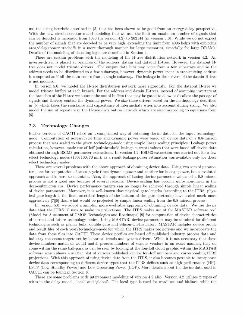
To facilitate better understanding of cache organization, version 5.0 can output data/tag array organizationgraphically. Figure 3 shows an example of the graphical display generated by version 5.0. The top part ofthe figure shows a generic mat organization assumed by CACTI. It is followed by the data and tag arrayorganization plotted based on array dimensions calculated by CACTI.
3 Data Array Organization
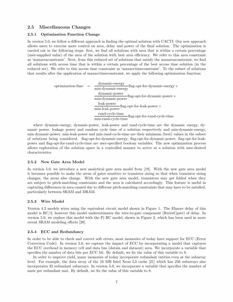
At the highest level, a data array is composed of multiple identical banks (Nbanks). Each bank can beconcurrently accessed and has its own address and data bus. Each bank is composed of multiple identicalsubbanks (Nsubbanks) with one subbank being activated per access. Each subbank is composed of multipleidentical mats (Nmats-in-subbank). All mats in a subbank are activated during an access with each mat holdingpart of the accessed word in the bank. Each mat itself is a self-contained memory structure composed of4 identical subarrays and associated predecoding logic. Each subarray is a 2D matrix of memory cells andassociated peripheral circuitry. Figure 4 shows the layout of an array with 4 banks. In this example eachbank is shown to have 4 subbanks and each subbbank is shown to have 4 mats. Not shown in Figure 4,address and data are assumed to be distributed to the mats on H-tree distribution networks.
The rest of this section further describes details of the array organization assumed in CACTI. Section3.1 describes the organization of a mat. Section 3.2 describes the organization of the H-tree distributionnetworks. Section 3.3 presents the different organizational parameters associated with a data array.
3.1 Mat Organization
Figure 5 shows the high-level composition of all mats. A mat is always composed of 4 subarrays andassociated predecoding/decoding logic which is located at the center of the mat. The predecoding/decodinglogic is shared by all 4 subarrays. The bottom subarrays are mirror images of the top subarrays and theleft hand side subarrays are mirror images of the right hand side ones. Not shown in this figure, by default,address/datain/dataout signals are assumed to enter the mat in the middle through its sides; alternatively,under user-control, it may also be specified to assume that they traverse over the memory cells.
Figure 6 shows the high-level composition of a subarray. The subarray consists of a 2D matrix ofthe memory cells and associated peripheral circuitry. Figure 7 shows the peripheral circuitry associatedwith bitlines of a subarray. After a wordline gets activated, memory cell data gets transferred to bitlines.
8
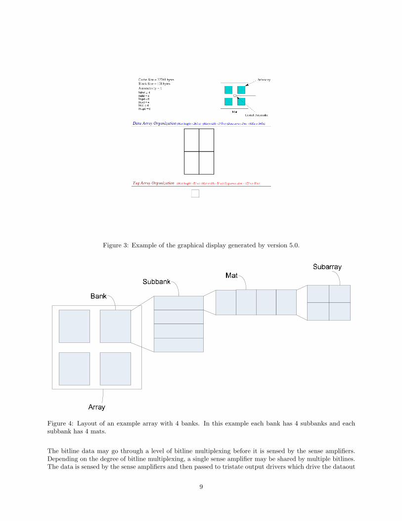
Figure 3: Example of the graphical display generated by version 5.0.
Figure 4: Layout of an example array with 4 banks. In this example each bank has 4 subbanks and eachsubbank has 4 mats.
The bitline data may go through a level of bitline multiplexing before it is sensed by the sense amplifiers.Depending on the degree of bitline multiplexing, a single sense amplifier may be shared by multiple bitlines.The data is sensed by the sense amplifiers and then passed to tristate output drivers which drive the dataout
9

Figure 5: High-level composition of a mat.
vertical H-tree (described later in this section). An additional level of multiplexing may be required at theoutputs of the sense amplifiers in organizations in which the bitline multiplexing is not sufficient to cullout the output data or in set-associative caches in which the output word from the correct way needs tobe selected. The select signals that control the multiplexing of the bitline mux and the sense amp mux aregenerated by the bitline mux select signals decoder and the sense amp mux select signals decoder respectively.When the degree of multiplexing after the outputs of the sense amplifiers is simply equal to the associativityof the cache, the sense amp mux select signal decoder does not have to decode any address bits and insteadsimply buffers the input way-select signals that arrive from the tag array.
Figure 6: High-level composition of a subarray.
10
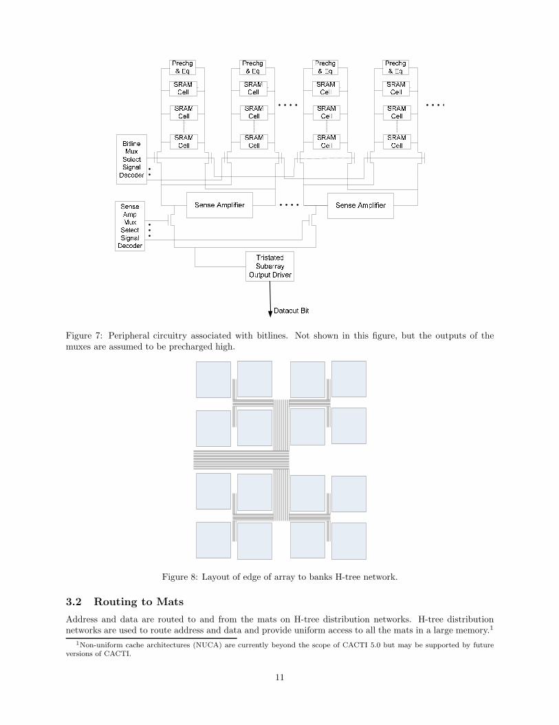
Figure 7: Peripheral circuitry associated with bitlines. Not shown in this figure, but the outputs of themuxes are assumed to be precharged high.
Figure 8: Layout of edge of array to banks H-tree network.
3.2 Routing to Mats
Address and data are routed to and from the mats on H-tree distribution networks. H-tree distributionnetworks are used to route address and data and provide uniform access to all the mats in a large memory.1
1Non-uniform cache architectures (NUCA) are currently beyond the scope of CACTI 5.0 but may be supported by futureversions of CACTI.
11
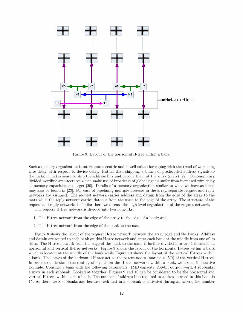
Figure 9: Layout of the horizontal H-tree within a bank.
Such a memory organization is interconnect-centric and is well-suited for coping with the trend of worseningwire delay with respect to device delay. Rather than shipping a bunch of predecoded address signals tothe mats, it makes sense to ship the address bits and decode them at the sinks (mats) [22]. Contemporarydivided wordline architectures which make use of broadcast of global signals suffer from increased wire delayas memory capacities get larger [20]. Details of a memory organization similar to what we have assumedmay also be found in [23]. For ease of pipelining multiple accesses in the array, separate request and replynetworks are assumed. The request network carries address and datain from the edge of the array to themats while the reply network carries dataout from the mats to the edge of the array. The structure of therequest and reply networks is similar; here we discuss the high-level organization of the request network.
The request H-tree network is divided into two networks:
1. The H-tree network from the edge of the array to the edge of a bank; and,
2. The H-tree network from the edge of the bank to the mats.
Figure 8 shows the layout of the request H-tree network between the array edge and the banks. Addressand datain are routed to each bank on this H-tree network and enter each bank at the middle from one of itssides. The H-tree network from the edge of the bank to the mats is further divided into two 1-dimensionalhorizontal and vertical H-tree networks. Figure 9 shows the layout of the horizontal H-tree within a bankwhich is located at the middle of the bank while Figure 10 shows the layout of the vertical H-trees withina bank. The leaves of the horizontal H-tree act as the parent nodes (marked as V0) of the vertical H-trees.In order to understand the routing of signals on the H-tree networks within a bank, we use an illustrativeexample. Consider a bank with the following parameters: 1MB capacity, 256-bit output word, 4 subbanks,4 mats in each subbank. Looked at together, Figures 9 and 10 can be considered to be the horizontal andvertical H-trees within such a bank. The number of address bits required to address a word in this bank is15. As there are 8 subbanks and because each mat in a subbank is activated during an access, the number
12

Figure 10: Layout of the vertical H-trees within a bank.
of address bits that need to be distributed to each mat is 12. Because each mat in a subbank produces 64out of the 256 output bits, the number of datain signals that need to be distributed to each mat is 64. Thus15 bits of address and 256 bits of datain enter the bank from the left side driven by the H0 node. At the H1node, the 15 address signals are redriven such that each of the two nodes H1 receive the 15 address signals.The datain signals split at node H1 and 32 datain signals go to the left H2 node and the other 32 go to theright H2 node. At each H2 node, the address signals are again redriven such that all of the 4 V0 nodes endup receiving the 15 address bits. The datain signals again split at each H2 node so that each V0 node endsup receiving 64 datain bits. These 15 address bits and 64 datain bits then traverse to each mat along the4 vertical H-trees. In the vertical H-trees, address and datain may either be assumed to be broadcast to allmats or alternatively, it may be assumed that these signals are appropriately gated so that they are routedto just the correct subbank that contains the data; by default, we assume the latter scenario.
The reply network H-trees are similar in principle to the request network H-trees. In case of the replynetwork vertical H-trees, dataout bits from each mat of a subbank travel on the vertical H-trees to the middleof the bank where they sink into the reply network horizontal H-tree, and are carried to the edge of thebank.
3.3 Organizational Parameters of a Data Array
In order to calculate the optimal organization based on a given objective function, like earlier versions ofCACTI [1][2][3][4], each bank is associated with partitioning parameters Ndwl, Ndbl and Nspd, where Ndwl =Number of segments in a bank wordline, Ndbl = Number of segments in a bank bitline, and Nspd = Numberof sets mapped to each bank wordline.
Unlike earlier versions of CACTI, in CACTI 5.0 Nspd can take on fractional values less than one. This isuseful for small highly-associative caches with large line sizes. Without values of Nspd less than one, memorymats with huge aspect ratios with only a few word lines but hundreds of bits per word line would be created.For a pure scratchpad memory (not a cache), Nspd is used to vary the aspect ratio of the memory bank.
13

Nsubbanks and Nmats-in-subbank are related to Ndwl and Ndbl as follows:
Nsubbanks =Ndbl
2(1)
Nmats-in-subbank =Ndwl
2(2)
Figure 11 shows different partitions of the same bank. The partitioning parameters are labeled alongside.Table 1 lists various organizational parameters associated with a data array.
Figure 11: Different partitions of a bank.
3.4 Comments about Organization of Data Array
The cache organization chosen in the CACTI model is a compromise between many possible different cacheorganizations. For example, in some organizations all the data bits could be read out of a single mat. Thiscould reduce dynamic power but increase routing requirements. On the other hand, organizations exist whereall mats are activated on a request and each produces part of the bits required. This obviously burns a lotof dynamic power, but has the smallest routing requirements. CACTI chooses a middle ground, where allthe bits for a read come from a single subbank, but multiple mats. Other more complicated organizations,in which predecoders are shared by two subarrays instead of four, or in which sense amplifiers are sharedbetween top and bottom subarrays, are also possible, however we try to model a simple common case inCACTI.
4 Circuit Models and Sizing
In Section 3, the high-level organization of an array was described. In this section, we delve deeper intologic and circuit design of the different entities. We also present the techniques adopted for sizing different
14
Parameter Name Meaning Parameter Type
Nbanks Number of banks User inputNdwl Number of divisions in a bank wordline Degree of freedomNdbl Number of divisions in a bank bitline Degree of freedomNspd Number of sets mapped to a bank wordline Degree of freedomDbitline-mux Degree of muxing at bitlines Degree of freedomNsubbanks Number of subbanks CalculatedNmats-in-subbank Number of mats in a subbank CalculatedNsubarr-rows Number of rows in a subarray CalculatedNsubarr-cols Number of columns in a subarray CalculatedDout-driv-mux Degree of bitline multiplexing Degree of freedomDout-driv-mux Degree of sense amp multiplexing CalculatedNsubarr-sense-amps Number of sense amplifiers in a subarray CalculatedNsubarr-out-drivers Number of output drivers in a subarray CalculatedNbank-addr-bits Number of address bits to a bank CalculatedNbank-datain-bits Number of datain bits to a mat CalculatedNbank-dataout-bits Number of dataout bits from a mat CalculatedNmat-addr-bits Number of address bits to a mat CalculatedNmat-datain-bits Number of datain bits to a mat CalculatedNmat-dataout-bits Number of dataout bits from a mat CalculatedNmat-way-select Number of way-select bits to a mat (for data array of cache) Calculated
Table 1: Organizational parameters of a data array.
circuits. The rest of this section is organized as follows: First, in Section 4.1, we describe the circuit modelthat we have assumed for wires. Next in Section 4.2, we describe the general philosophy that we haveadopted for sizing circuits. Next in Section 4.3, we describe the circuit models and sizing techniques for thedifferent circuits within a mat, and in Section 4.5, we describe them for the circuits used in the differentH-tree networks.
4.1 Wire Modeling
Wires are considered to belong to one of two types: ideal or non-ideal. Ideal wires are assumed to have zeroresistance and capacitance. Non-ideal wires are assumed to have finite resistance and capacitance and aremodeled using a one-section Pi RC model shown in Figure 12. In this figure, Rwire and Cwire for a wire oflength Lwire are given by the following equations:
Rwire = LwireRunit-length-wire (3)
Cwire = LwireCunit-length-wire (4)
Figure 12: One-section Pi RC model that we have assumed for non-ideal wires.
For computation of Runit-length-wire and Cunit-length-wire wires, we use the equations presented in [6][12]which are reproduced below. Figure 13 shows the accompanying picture for the capacitance model from [6].
15
Runit-length-wire = αscatter
ρ
(thickness − barrier − dishing)(width − 2 ∗ barrier)(5)
Cunit-length-wire = ǫ0(2Mǫhoriz
thickness
spacing+ 2ǫvert
width
ILDthick
) + fringe(ǫhoriz, ǫvert) (6)
Figure 13: Capacitance model from [6].
4.2 Sizing Philosophy
In general the sizing of circuits depends on various optimization goals: circuits may be sized for minimumdelay, minimum energy-delay product, etc. CACTI’s goal is to model simple representative circuit sizingapplicable to a broad range of common applications. As in earlier SRAM modeling efforts [5][20][24], wehave made extensive use of the method of logical effort in sizing different circuit blocks. Explanation of themethod of logical effort may be found in [25].
4.3 Sizing of Mat Circuits
As described earlier in Section 3.1, a mat is composed of entities such as the predecoding/decoding logic,memory cell array and bitline peripheral circuitry. We present circuits, models and sizing techniques forthese entities.
4.3.1 Predecoder and Decoder
As discussed in Section 2, new circuit structures have been adopted for the decoding logic. The same decodinglogic circuit structures are utilized for producing the row-decode signals and the select signals of the bitlineand sense amplifier muxes. In the discussion here, we focus on the row-decoding logic. In order to describethe circuit structures assumed within the different entities of the row-decoding logic, we use an illustrativeexample. Figure 14 shows the structure of the row-decoding logic for a subarray with 1024 rows. Therow-decoding logic is composed of two row-predecode blocks and the row-decode gates and drivers. The row-predecode blocks are responsible for predecoding the address bits and generating predecoded signals. Therow-decode gates and drivers are responsible for decoding the predecoded outputs and driving the wordlineload. Each row-predecode block can predecode a maximum of 9 bits and has a 2-level logic structure. With1024 rows, the number of address bits required for row-decoding is 10. Figure 15 shows the structure of eachrow predecode block for a subarray with 1024 rows. Each row predecode block is responsible for predecoding5 address bits and each of them generates 32 predecoded output bits. Each predecode block has two levels.
16

The first level is composed of one 2-4 decode unit and one 3-8 decode unit. At the second level, the 4 outputsfrom the 2-4 decode unit and the 8 outputs from the 3-8 decode unit are combined together using 32 NAND2gates in order to produce the 32 predecoded outputs. The 32 predecoded outputs from each predecode blockare combined together using the 1024 NAND2 gates to generate the row decode signals.
Figure 14: Structure of the row decoding logic for a subarray with 1024 rows.
Figure 17 shows the circuit paths in the decoding logic for the subarray with 1024 rows. One of the pathscontains the NAND2 of the 2-4 decode unit and the other contains the NAND3 gate of the 3-8 decode unit.Each path has 3 stages in its path. The branching efforts at the outputs of the first two stages are alsoshown in the figure. The predecode output wire is treated as a non-ideal wire with its Rpredec-out-wire andCpredec-out-wire computed using the following equations:
Rpredec-output-wire = Lpredec-output-wireRunit-length-wire (7)
Cpredec-output-wire = Lpredec-output-wireCunit-length-wire (8)
where Lpredec-output-wire is the maximum length amongst lengths of predecode output wires.The sizing of gates in each circuit path is calculated using the method of logical effort. In each of the 3
stages of each circuit path, minimum-size transistors are assumed at the input of the stage and each stageis sized independent of each other using the method of logical effort. While this is not optimal from a delaypoint of view, it is simpler to model and has been found to be a good sizing heuristic from an energy-delaypoint of view [5].
In this example that we considered for decoding logic of a subarray with 1024 rows, there were twodifferent circuit paths, one involving the NAND2 gate and another involving the NAND3 gate. In thegeneral case, when each predecode block decodes different number of address bits, a maximum of four circuitpaths may exist. When the degree of decoding is low, some of the circuit blocks shown in Figure 14 may notbe required. For example, Figure 16 shows the decoding logic for a subarray with 8 rows. In this case, thedecoding logic simply involves a 3-8 decode unit as shown.
17

Figure 15: Structure of the row predecode block for a subarray with 1024 rows.
As mentioned before, the same circuit structures used within the row-decoding logic are also used forgenerating the select signals of the bitline and sense amplifier muxes. However, unlike the row-decodinglogic in which the NAND2 decode gates and drivers are assumed to be placed on the side of subarray, theNAND2 decode gates and drivers are assumed to be placed at the center of the mat near their correspondingpredecode blocks. Also, the resistance/capacitance of the wires between the predecode blocks and the decodegates are not modeled and are assumed to be zero.
4.3.2 Bitline Peripheral Circuitry
Memory Cell Figure 18 shows the circuit assumed for a 1-ported SRAM cell. The transistors of theSRAM cell are sized based on the widths specified in [17] and are presented in Section 8.
18

Figure 16: Structure of the row-decoding logic for a subarray with 8 rows. The row-decoding logic is simplycomposed of 8 decode gates and drivers.
Figure 17: Row decoding logic circuit paths for a subarray with 1024 rows. One of the circuit paths containsthe NAND2 gate of the 2-4 decode unit while the other contains the NAND3 gate of the 3-8 decode unit.
Sense Amplifier Figure 19 shows the circuit assumed for a sense amplifier - it’s a clocked latch-basedsense amplifier. When the ENABLE signal is not active, there is no flow of current through the transistorsof the latch. The small-signal circuit model and analysis of this latch-based sense amplifier is presented inSection 4.4.
Bitline and Sense Amplifier Muxes Figure 20 shows the circuit assumed for the bitline and senseamplifier muxes. We assume that the mux is implemented using NMOS pass transistors. The use of NMOS
19

Figure 18: 1-ported 6T SRAM cell
!"#$%&$'$ !"#$%&$'$
Figure 19: Clocked latch-based sense amplifier
transistors implies that the output of the mux needs to be precharged high in order to avoid degraded ones.We do not attempt to size the transistors in the muxes and instead assume (as in [20]) fixed widths for theNMOS transistors across all partitions of the array.
Precharge and Equalization Circuitry Figure 21 shows the circuit assumed for precharging and equal-izing the bitlines. The bitlines are assumed to be precharged to VDD through the PMOS transistors. Just likethe transistors in the bitline and sense amp muxes, we do not attempt to size the precharge and equalizationtransistors and instead assume fixed-width transistors across different partitions of the array.
20

Figure 20: NMOS-based mux. The output is assumed to be precharged high.
Figure 21: Bitlines precharge and equalization circuitry.
Bitlines Read Path Circuit Model Figure 22 shows the circuit model for the bitline read path betweenthe memory cell and the sense amplifier mux.
4.4 Sense Amplifier Circuit Model
Figure 19 showed the clocked latch-based sense amplifier that we have assumed. [26] presents analysis of thiscircuit and equations for sensing delay under different assumptions. Figure 23 shows one of the small-signalmodels presented in [26]. Use of this small-signal model is based on two assumptions:
1. Current has been flowing in the circuit for a sufficiently long time; and
2. The equilibriating device can be modeled as an ideal switch.
For the small-signal model of Figure 23, it has been shown that the delay of the sensing operation isgiven by the following equation:
Tsense =Csense
Gm
ln(VDD
Vsense
) (9)
Use of this equation for calculation of sense amplifier delay requires that the value of Gmn and Gmp
for the circuit be known. We assume that the transistors in the sense amplifier latch exhibit short-channeleffects. For a transistor that exhibits short-channel effect, we use the following typical current equation [27]for computation of saturation current:
Idsat =µeff
2Cox
W
L(VGS − VTH)Vdsat (10)
21
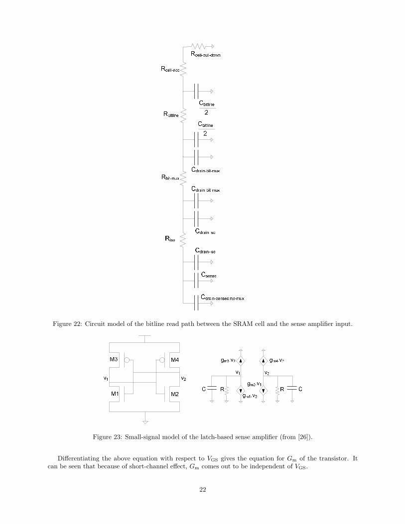
Figure 22: Circuit model of the bitline read path between the SRAM cell and the sense amplifier input.
Figure 23: Small-signal model of the latch-based sense amplifier (from [26]).
Differentiating the above equation with respect to VGS gives the equation for Gm of the transistor. Itcan be seen that because of short-channel effect, Gm comes out to be independent of VGS.
22

Gm =µeff
2Cox
W
LVdsat (11)
4.5 Routing Networks
As described earlier in Section 3.2, address and data are routed to and from the mats on H-tree distributionnetworks. First address/data are routed on an H-tree from array edge to bank edge and then on anotherH-tree from bank edge to the mats.
4.5.1 Array Edge to Bank Edge H-tree
Figure 8 showed the layout of H-tree distribution of address and data between the array edge and the banks.This H-tree network is assumed to be composed of inverter-based repeaters. The sizing of the repeaters andthe separation distance between them is determined based on the formulae given in [6]. In order to allow forenergy-delay tradeoffs in the repeater design, we introduce an user-controlled variable “maximum percentageof delay away from best repeater solution” or ‘maxrepeaterdelayconstraint’ in short. A maxrepeaterdelaycon-straint of zero results in the best delay repeater solution. For a maxrepeaterdelayconstraint of 10%, the delayof the path is allowed to get worse by a maximum of 10% with respect to the best delay repeater solutionby reducing the sizing and increasing the separation distance. Thus, with the maxrepeaterdelayconstraint,limited energy savings are possible at the expense of delay.
4.5.2 Bank Edge to Mat H-tree
Figures 9 and 10 showed layout examples of horizontal and vertical H-trees within a bank, each with 3 nodes.We assume that drivers are placed at each of the nodes of these H-trees. Figure 24 shows the circuit path anddriver circuit structure of the address/datain H-trees, and Figure 25 shows the circuit path and driver circuitstructure of the vertical dataout H-tree. In order to allow for signal-gating in the address/datain H-trees weconsider multi-stage buffers with a 2-input NAND gate as the input stage. The sizing and number of gatesat each node of the H-trees is computed using the methodology described in [5] which takes into account theresistance and capacitance of the intermediate wires in the H-tree.
Figure 24: Circuit path of address/datain H-trees within a bank.
One problem with the circuit paths of Figures 24 and 25 is that they start experiencing increased wiredelays as the wire lengths between the drivers start to get long. This also limits the maximum random cycletime that can be achieved for the array. So, as an alternative to modeling drivers only at H-tree branchingnodes, we also consider an alternative model in which the H-tree circuit paths within a bank are composed ofbuffers at regular intervals (i.e. repeaters). With repeaters, the delay through the H-tree paths within a bankcan be reduced at the expense of increased power consumption. Figure 26 shows the different types of buffercircuits that have been modeled in the H-tree path. At the branches of the H-tree, we again assume bufferswith a NAND gate in the input stage in order to allow for signal-gating whereas in the H-tree segmentsbetween two nodes, we model inverter-based buffers. We again size these buffers according to the buffersizing formulae given in [6]. The maxrepeaterdelayconstraint that was described in Section 4.5.1 is also usedhere to decide the sizing of the buffers and their separation distance so that delay in these H-trees also maybe traded off for potential energy savings.
23
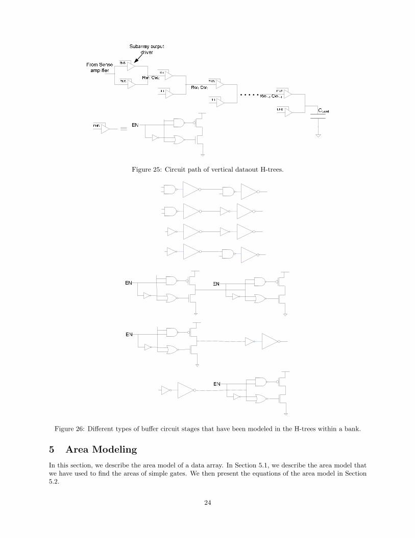
Figure 25: Circuit path of vertical dataout H-trees.
Figure 26: Different types of buffer circuit stages that have been modeled in the H-trees within a bank.
5 Area Modeling
In this section, we describe the area model of a data array. In Section 5.1, we describe the area model thatwe have used to find the areas of simple gates. We then present the equations of the area model in Section5.2.
24

5.1 Gate Area Model
A new area model has been used to estimate the areas of transistors and gates such as inverter, NANDand NOR gates. This area model is based off a layout model from [19] which describes a fast technique toestimate standard cell characteristics before the cells are actually laid out. Figure 27 illustrates the layoutmodel that has been used in [19]. Table 2 shows the process/technology input parameters required by thisgate area model. For a thorough description of the technique, please refer to [19]. Gates with stackedtransistors are assumed to have a layout similar to that described in [1]. When a transistor width exceedsa certain maximum value (Hn-diff for NMOS and Hp-diff for PMOS in Table 2), the transistor is assumedto be folded. This maximum value can either be process-specific or context-specific. An example of when acontext-specific width would be used is in case of memory sense amplifiers which typically have to be laidout at a certain pitch.
()**+,)-./0123)/24
560.,),4-663/)-.23)/24
Figure 27: Layout model assumed for gates (from [19]).
Parameter name Meaning
Hn-diff Maximum height of n diffusion of a transistorHp-diff Maximum height of p diffusion for a transistorHgap-bet-same-diffs Minimum gap between diffusions of the same typeHgap-bet-opp-diffs Minimum gap between n and p diffusionsHpower-rail Height of VDD (GND) power railWp Minimum width of poly (poly half-pitch or process feature size)Sp-p Minimum poly-to-poly spacingWc Contact widthSp-c Minimum poly-to-contact spacing
Table 2: Process/technology input parameters required by the gate area model.
Given the width of an NMOS transistor, Wbefore-folding, the number of folded transistors may be calculatedas follows:
Nfolded-transistors = ⌈Wbefore-folding
Hn-diff
⌉ (12)
The equation for total diffusion width of Nstacked transistors when they are not folded is given by thefollowing equation:
25
total-diff-width = 2(Wc + 2Sp-c) + NstackedWp + (Nstacked − 1)Sp-p (13)
The equation for total diffusion width of Nstacked transistors when they are folded is given by the followingequation:
total-diff-width = 2Nfolded-transistors(Wc + 2Sp-c) + Nfolded-transistorsNstackedWp +
Nfolded-transistors(Nstacked − 1)Sp-p (14)
Note that Equation 14 is a generalized form of the equations used for calculating diffusion width (forcomputation of drain capacitance) in the original CACTI report [1]. Earlier versions of CACTI assumed atmost two folded transistors; in version 5.0, we allow the degree of folding to be greater than 2 and makethe associated layout and area models more general. Note that drain capacitance calculation in version 5.0makes use of equations similar to 13 and 14 for computation of diffusion width.
The height of a gate is calculated using the following equation:
Hgate = Hn-diff + Hp-diff + Hgap-bet-opp-diffs + 2Hpower-rail (15)
5.2 Area Model Equations
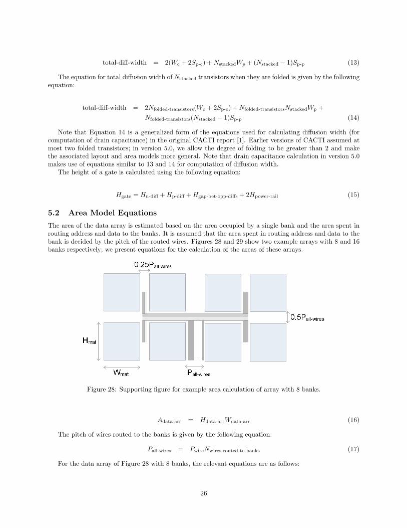
The area of the data array is estimated based on the area occupied by a single bank and the area spent inrouting address and data to the banks. It is assumed that the area spent in routing address and data to thebank is decided by the pitch of the routed wires. Figures 28 and 29 show two example arrays with 8 and 16banks respectively; we present equations for the calculation of the areas of these arrays.
Figure 28: Supporting figure for example area calculation of array with 8 banks.
Adata-arr = Hdata-arrWdata-arr (16)
The pitch of wires routed to the banks is given by the following equation:
Pall-wires = PwireNwires-routed-to-banks (17)
For the data array of Figure 28 with 8 banks, the relevant equations are as follows:
26

Figure 29: Supporting figure for example area calculation of array with 16 banks.
Wdata-arr = 4Wbank + Pall-wires + 2Pall-wires
4(18)
Hdata-arr = 2Hbank +Pall-wires
2(19)
Nwires-routed-to-banks = 8(Nbank-addr-bits + Nbank-datain-bits + Nbank-dataout-bits +
Nway-select-signals) (20)
For the data array of Figure 29 with 16 banks, the relevant equations are as follows:
Hdata-arr = 4Hbank + Pall-wires + 2Pall-wires
4(21)
Wdata-arr = 4Wbank +Pall-wires
2+ 2
Pall-wires
8(22)
Nwires-routed-to-banks = 16(Nbank-addr-bits + Nbank-datain-bits + Nbank-dataout-bits +
Nway-select-signals) (23)
The banks in a data array are assumed to be placed in such a way that the number of banks in thehorizontal direction is always either equal to or twice the number of banks in the vertical direction. Theheight and width of a bank is calculated by computing the area occupied by the mats and the area occupied
27
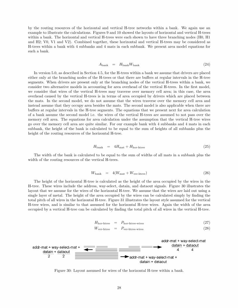
by the routing resources of the horizontal and vertical H-tree networks within a bank. We again use anexample to illustrate the calculations. Figures 9 and 10 showed the layouts of horizontal and vertical H-treeswithin a bank. The horizontal and vertical H-trees were each shown to have three branching nodes (H0, H1and H2; V0, V1 and V2). Combined together, these horizontal and vertical H-trees may be considered asH-trees within a bank with 4 subbanks and 4 mats in each subbank. We present area model equations forsuch a bank.
Abank = HbankWbank (24)
In version 5.0, as described in Section 4.5, for the H-trees within a bank we assume that drivers are placedeither only at the branching nodes of the H-trees or that there are buffers at regular intervals in the H-treesegments. When drivers are present only at the branching nodes of the vertical H-trees within a bank, weconsider two alternative models in accounting for area overhead of the vertical H-trees. In the first model,we consider that wires of the vertical H-trees may traverse over memory cell area; in this case, the areaoverhead caused by the vertical H-trees is in terms of area occupied by drivers which are placed betweenthe mats. In the second model, we do not assume that the wires traverse over the memory cell area andinstead assume that they occupy area besides the mats. The second model is also applicable when there arebuffers at regular intervals in the H-tree segments. The equations that we present next for area calculationof a bank assume the second model i.e. the wires of the vertical H-trees are assumed to not pass over thememory cell area. The equations for area calculation under the assumption that the vertical H-tree wiresgo over the memory cell area are quite similar. For our example bank with 4 subbanks and 4 mats in eachsubbank, the height of the bank is calculated to be equal to the sum of heights of all subbanks plus theheight of the routing resources of the horizontal H-tree.
Hbank = 4Hmat + Hhor-htree (25)
The width of the bank is calculated to be equal to the sum of widths of all mats in a subbank plus thewidth of the routing resources of the vertical H-trees.
Wbank = 4(Wmat + Wver-htree) (26)
The height of the horizontal H-tree is calculated as the height of the area occupied by the wires in theH-tree. These wires include the address, way-select, datain, and dataout signals. Figure 30 illustrates thelayout that we assume for the wires of the horizontal H-tree. We assume that the wires are laid out using asingle layer of metal. The height of the area occupied by the wires can be calculated simply by finding thetotal pitch of all wires in the horizontal H-tree. Figure 31 illustrates the layout style assumed for the verticalH-tree wires, and is similar to that assumed for the horizontal H-tree wires. Again the width of the areaoccupied by a vertical H-tree can be calculated by finding the total pitch of all wires in the vertical H-tree.
Hhor-htree = Phor-htree-wires (27)
Wver-htree = Pver-htree-wires (28)
Figure 30: Layout assumed for wires of the horizontal H-tree within a bank.
28

Figure 31: Layout assumed for wires of the vertical H-tree within a bank.
The height and width of a mat are estimated using the following equations. Figure 32 shows the layout ofa mat and illustrates the assumptions made in the following equations. We assume that half of the address,way-select, datain and dataout signals enter the mat from its left and the other half enter from the right.
Wmat =HmatWmat-initial + Amat-center-circuitry
Winitial-mat
(29)
Hmat = 2Hsubarr-mem-cell-area + Hmat-non-cell-area (30)
Winitial-mat = 2Wsubarr-mem-cell-area + Wmat-non-cell-area (31)
Amat-center-circuitry = Arow-predec-block-1 + Arow-predec-block-2
+Abit-mux-predec-block-1 + Abit-mux-predec-block-2
+Asenseamp-mux-predec-block-1 + Asenseamp-mux-predec-block-2 +
Abit-mux-dec-drivers + Asenseamp-mux-dec-drivers (32)
Hsubarr−mem−cell−area = Nsubarr-rowsHmem-cell (33)
Wsubarr−mem−cell−area = Nsubarr-colsWmem-cell + ⌊Nsubarr-cols
Nmem-cells-per-wordline-stitch
⌋Wwordline-stitch +
⌈Nsubarr-cols
Nbits-per-ecc-bit
⌉Wmem-cell (34)
Hmat-non-cell-area = 2Hsubarr-bitline-peri-circ + Hhor-wires-within-mat (35)
Hhor-wires-within-mat = Hbit-mux-sel-wires + Hsenseamp-mux-sel-wires + Hwrite-mux-sel-wires +
Hnumber-mat-addr-bits
2+
Hnumber-way-select-signals
2+
Hnumber-mat-datain-bits
2+
Hnumber-mat-dataout-bits
2(36)
Wmat-non-cell-area = max(2Wsubarr-row-decoder, Wrow-predec-out-wires) (37)
Hsubarr-bitline-peri-cir = Hbit-mux + Hsenseamp-mux + Hbitline-pre-eq + Hwrite-driver + Hwrite-mux (38)
Note that the width of the mat is computed as in Equation 30 because we optimistically assume that the
29

Figure 32: Layout of a mat.
circuitry laid out at the center of the mat does not lead to white space in the mat. The areas of lower-levelcircuit blocks such as the bitline and sense amplifier muxes and write drivers are calculated using the areamodel that was described in Section 5.1 while taking into account pitch-matching constraints.
When redundancy in mats is also considered, the following area contribution due to redundant mats isadded to the area of the data array computed in Equation 16.
Aredundant-mats = Nredundant-matsAmat (39)
Nredundant-mats = ⌊Nbanks
Nmats
Nmats-per-redundant-mat⌋ (40)
where Nmats-per-redundant-mat is the number of mats per redundant mat that and is set to 8 by default.The final height of the data array is readjusted under the optimistic assumption that the redundant matsdo not cause any white space in the data array.
Hdata-arr =Adata-arr
Wdata-arr
(41)
6 Delay Modeling
In this section we present equations used in CACTI to calculate access time and random cycle time of amemory array.
6.1 Access Time Equations
Taccess = Trequest-network + Tmat + Treply-network (42)
Trequest-network = Tarr-edge-to-bank-edge-htree + Tbank-addr-din-hor-htree + Tbank-addr-din-ver-htree (43)
Tmat = max(Trow-decoder-path, Tbit-mux-decoder-path, Tsense-amp-decoder-path) (44)
Treply-network = Tbank-dout-ver-htree + Tbank-dout-hor-htree + Tbank-edge-to-arr-edge (45)
The critical path in the mat usually involves the wordline and bitline access. However, Equation 44 alsomust include a max with the delays of the bitline mux decoder and sense amp mux decoder paths as these
30
circuits operate in parallel with the row decoding logic, and in general may act as the critical path for certainpartitions of the data array. Usually when that happens, the number of rows in the subarray would be toofew and the partitions would not get selected.
Trow-decoder-path = Trow-predec + Trow-dec-driver + Tbitline + Tsense-amp (46)
Tbit-mux-decoder-path = Tbit-mux-predec + Tbit-mux-dec-driver + Tsense-amp (47)
Tsenseamp-mux-decoder-path = Tsenseamp-mux-predec + Tsenseamp-mux-dec-driver (48)
Trow-predec = max(Trow-predec-blk-1-nand2-path, Trow-predec-blk-1-nand3-path,
Trow-predec-blk-2-nand2-path, Trow-predec-blk-2-nand3-path) (49)
Tbit-mux-sel-predec = max(Tbit-mux-sel-predec-blk-1-nand2-path, Tbit-mux-sel-predec-blk-1-nand3-path,
Tbit-mux-sel-predec-blk-2-nand2-path, Tbit-mux-sel-predec-blk-2-nand3-path) (50)
Tsenseamp-mux-sel-predec = max(Tsenseamp-mux-sel-predec-blk-1-nand2-path, Tsenseamp-mux-sel-predec-blk-1-nand3-path,
Tsenseamp-mux-sel-predec-blk-2-nand2-path, Tsenseamp-mux-sel-predec-blk-2-nand3-path) (51)
The calculation for bitline delay is based on the model described in [28]. The model considers the effectof the wordline rise time.
Tbitline =
√
2TstepVDD−VTH
mif Tstep <= 0.5V DD−VTH
m
Tstep + VDD−VTH
2mif Tstep > 0.5V DD−VTH
m
(52)
Tstep = (Rcell-pull-down + Rcell-acc)(Cbitline + 2Cdrain-bit-mux + Ciso + Csense + Cdrain-senseamp-mux) +
Rbitline(Cbitline
2+ 2Cdrain-bit-mux + Ciso + Csense + Cdrain-senseamp-mux) +
Rbit-mux(Cdrain-bit-mux + Ciso + Csense + Cdrain-senseamp-mux) + Riso(Ciso + Csense +
Cdrain-senseamp-mux) (53)
m =VDD − VTH
2Tstep
(54)
The calculation of sense amplifier delay makes use of the model described in [26].
Tsense = τln(VDD
Vsense
) (55)
τ =Csense
Gm
(56)
6.2 Random Cycle Time Equations
Typically, the random cycle time of an SRAM would be limited by wordline and bitline delays. In order tocome up with an equation for lower bound on random cycle time, we consider that the SRAM is potentiallypipelineable with placement of latches at appropriate locations.
Trandom-cycle = max(Trow-dec-driver + Tbitline + Tsense-amp + Twordline-reset +
max(Tbitline-precharge, Tbit-mux-out-precharge, Tsenseamp-mux-out-precharge),
Tbetween-buffers-bank-hor-htree, Tbetween-buffers-bank-ver-dataout-htree, Trow-predec-blk,
Tbit-mux-predec-blk + Tbit-mux-dec-driver,
Tsenseamp-mux-predec-blk + Tsenseamp-mux-dec-driver) (57)
31

We come up with an estimate for the wordline reset delay by assuming that the wordline dischargesthrough the NMOS transistor of the final inverter in the wordline driver.
Twordline-reset = ln(VDD − 0.1VDD
VDD)(Rfinal-inv-wordline-driverCwordline +
Rfinal-inv-wordline-driverCwordline
2)
Tbitline-precharge = ln(VDD − 0.1Vbitline-swing
VDD − Vbitline-swing
)(Rbit-preCbitline +RbitlineCbitline
2) (58)
Tbit-mux-out-precharge = ln(VDD − 0.1Vbitline-swing
VDD − Vbitline-swing
)(Rbit-mux-preCbit-mux-out +
Rbit-mux-outCbit-mux-out
2) (59)
Tsenseamp-mux-out-precharge = ln(VDD − 0.1Vbitline-swing
VDD − Vbitline-swing
)(Rsenseamp-mux-preCsenseamp-mux-out +
Rsenseamp-mux-outCsenseamp-mux-out
2) (60)
7 Power Modeling
In this section, we present the equations used in CACTI to calculate dynamic power and leakage power of adata array. Here we present equations for dynamic read power; the equations for dynamic write power aresimilar.
Pread =Edyn-read
Trandom-cycle
+ Pleak (61)
where Edyn-read is the dynamic read energy per access of the array, Trandom-cycle is the random cycle timeof the array and Pleak is the leakage power in the array.
7.1 Calculation of Dynamic Energy
7.1.1 Dynamic Energy Calculation Example for a CMOS Gate Stage
We present a representative example to illustrate how we calculate the dynamic energy for a CMOS gatestage. Figure 33 shows a CMOS gate stage composed of a NAND2 gate followed by an inverter which drivesthe load. The energy consumption of this circuit is given by:
Edyn = Edyn-nand2 + Edyn-inv (62)
Edyn-nand2 = 0.5(Cintrinsic-nand2 + Cgate-inv)VDD2 (63)
Edyn-inv = 0.5(Cintrinsic-inv + Cgate-load-next-stage + Cwire-load)VDD2 (64)
Cinstrinsic-nand2 = draincap(nand2, Wnand-pmos, Wnand-nmos) (65)
Cgate-inv = gatecap(inv, Winv-pmos, Winv-nmos) (66)
Cdrain-inv = draincap(inv, Winv-pmos, Winv-nmos) (67)
The multiplicative factor of 0.5 in the equations of Edyn-nand2 and Edyn-inv assumes consecutive chargingand discharging cycles for each gate. Energy is consumed only during the charging cycle of a gate when itsoutput goes from low to high.
32
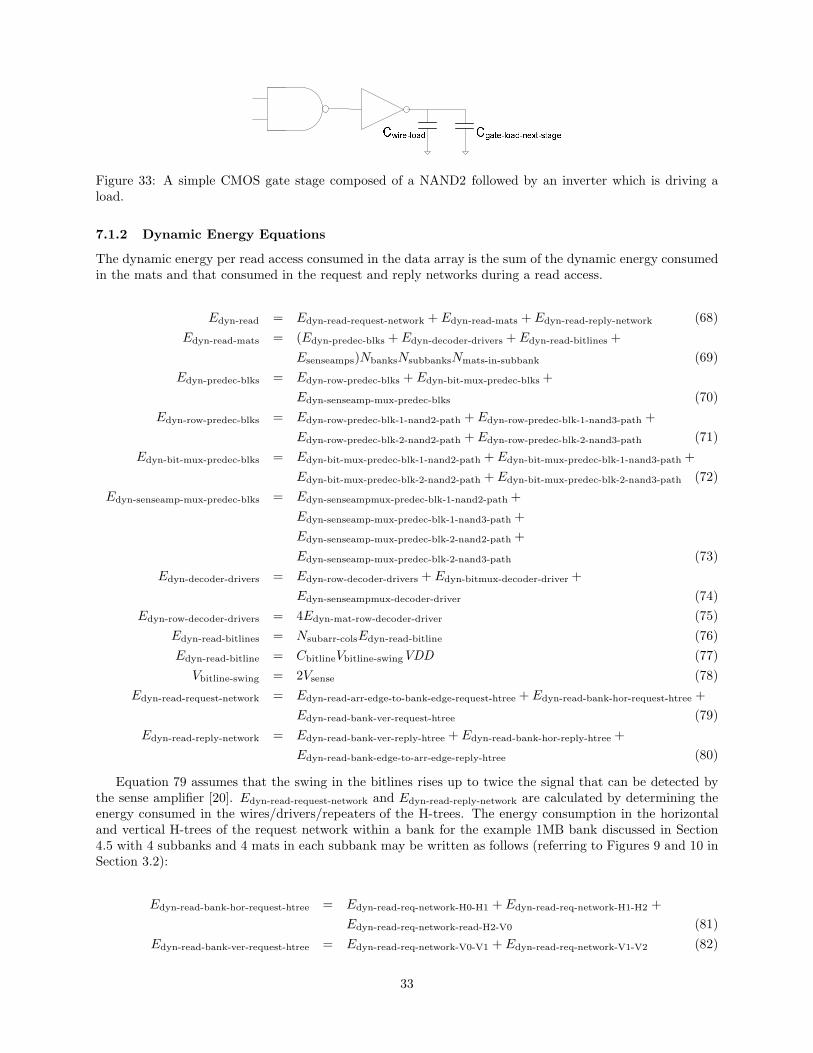
Figure 33: A simple CMOS gate stage composed of a NAND2 followed by an inverter which is driving aload.
7.1.2 Dynamic Energy Equations
The dynamic energy per read access consumed in the data array is the sum of the dynamic energy consumedin the mats and that consumed in the request and reply networks during a read access.
Edyn-read = Edyn-read-request-network + Edyn-read-mats + Edyn-read-reply-network (68)
Edyn-read-mats = (Edyn-predec-blks + Edyn-decoder-drivers + Edyn-read-bitlines +
Esenseamps)NbanksNsubbanksNmats-in-subbank (69)
Edyn-predec-blks = Edyn-row-predec-blks + Edyn-bit-mux-predec-blks +
Edyn-senseamp-mux-predec-blks (70)
Edyn-row-predec-blks = Edyn-row-predec-blk-1-nand2-path + Edyn-row-predec-blk-1-nand3-path +
Edyn-row-predec-blk-2-nand2-path + Edyn-row-predec-blk-2-nand3-path (71)
Edyn-bit-mux-predec-blks = Edyn-bit-mux-predec-blk-1-nand2-path + Edyn-bit-mux-predec-blk-1-nand3-path +
Edyn-bit-mux-predec-blk-2-nand2-path + Edyn-bit-mux-predec-blk-2-nand3-path (72)
Edyn-senseamp-mux-predec-blks = Edyn-senseampmux-predec-blk-1-nand2-path +
Edyn-senseamp-mux-predec-blk-1-nand3-path +
Edyn-senseamp-mux-predec-blk-2-nand2-path +
Edyn-senseamp-mux-predec-blk-2-nand3-path (73)
Edyn-decoder-drivers = Edyn-row-decoder-drivers + Edyn-bitmux-decoder-driver +
Edyn-senseampmux-decoder-driver (74)
Edyn-row-decoder-drivers = 4Edyn-mat-row-decoder-driver (75)
Edyn-read-bitlines = Nsubarr-colsEdyn-read-bitline (76)
Edyn-read-bitline = CbitlineVbitline-swingVDD (77)
Vbitline-swing = 2Vsense (78)
Edyn-read-request-network = Edyn-read-arr-edge-to-bank-edge-request-htree + Edyn-read-bank-hor-request-htree +
Edyn-read-bank-ver-request-htree (79)
Edyn-read-reply-network = Edyn-read-bank-ver-reply-htree + Edyn-read-bank-hor-reply-htree +
Edyn-read-bank-edge-to-arr-edge-reply-htree (80)
Equation 79 assumes that the swing in the bitlines rises up to twice the signal that can be detected bythe sense amplifier [20]. Edyn-read-request-network and Edyn-read-reply-network are calculated by determining theenergy consumed in the wires/drivers/repeaters of the H-trees. The energy consumption in the horizontaland vertical H-trees of the request network within a bank for the example 1MB bank discussed in Section4.5 with 4 subbanks and 4 mats in each subbank may be written as follows (referring to Figures 9 and 10 inSection 3.2):
Edyn-read-bank-hor-request-htree = Edyn-read-req-network-H0-H1 + Edyn-read-req-network-H1-H2 +
Edyn-read-req-network-read-H2-V0 (81)
Edyn-read-bank-ver-request-htree = Edyn-read-req-network-V0-V1 + Edyn-read-req-network-V1-V2 (82)
33

The energy consumed in the H-tree segments depends on the location of the segment in the H-treeand the number of signals that are transmitted in each segment. In the request network, during a readaccess, between nodes H0 and H1, a total of 15 (address) signals are transmitted; between node H1 andboth H2 nodes, a total of 30 (address) signals are transmitted; between all H2 and V0 nodes, a total of 60(address) signals are transmitted. In the vertical H-tree, we assume signal-gating so that the address bits aretransmitted to the mats of a single subbank only; thus, between all V0 and V1 nodes, a total of 56 (address)signals are transmitted; between all V1 and V2 nodes, a total of 52 (address) signals are transmitted.
Edyn-read-req-network-H0-H1 = (15)EH0-H1-1-bit (83)
Edyn-read-req-network-H1-H2 = (30)EH1-H2-1-bit (84)
Edyn-read-req-network-H2-V0 = (60)EH2-V0-1-bit (85)
Edyn-read-req-network-V0-V1 = (56)EV0-V1-1-bit (86)
Edyn-read-req-network-V1-V2 = (52)EV1-V2-1-bit (87)
The equations for energy consumed in the H-trees of the reply network are similar in form to the aboveequations. Also, the equations for dynamic energy per write access are similar to the ones that have beenpresented here for read access. In case of write access, the datain bits are written into the memory cells atfull swing of the bitlines.
7.2 Calculation of Leakage Power
We estimate the standby leakage power consumed in the array. Our leakage power estimation does notconsider the use of any leakage control mechanism in the array. We make use of the methodology presentedin [29][24] to simply provide an estimate of the drain-to-source subthreshold leakage current for all transistorsthat are off with VDD applied across their drain and source.
7.2.1 Leakage Power Calculation for CMOS gates
We illustrate our methodology of calculation of leakage power for the CMOS gates that are used in ourmodeling. Figure 34 illustrates the leakage power calculation for an inverter. When the input is low andthe output is high, there is subthreshold leakage through the NMOS transistor whereas when the input ishigh and the output is low, there is subthreshold leakage current through the PMOS transistor. In order tosimplify our modeling, we come up with a single average leakage power number for each gate. Thus for theinverter, we calculate leakage as follows:
Pleak-inv =Winv-pmosIoff-pmos + Winv-nmosIoff-nmos
2(88)
where Ioff-pmos is the subthreshold current per unit width for the PMOS transistor and Ioff-nmos is thesubthreshold current per unit width for the NMOS transistor.
Figure 35 illustrates the leakage power calculation for a NAND2 gate. When both inputs are high, theoutput is low and for this condition there is leakage through the PMOS transistors as shown. When eitherof the inputs is low, the output is high and there is leakage through the NMOS transistors. Because of thestacked NMOS transistors [29][24], this leakage depends on which input(s) is low. The leakage is least whenboth inputs are low. Under standby operating conditions, for NAND2 and NAND3 gates in the decodinglogic within the mats, we assume that the output of each NAND is high (deactivated) with both of its inputslow. Thus we attribute a leakage number to the NAND gate based on the leakage through its stacked NMOStransistors when both inputs are low. We consider the reduction in leakage due to the effect of stackedtransistors and calculate leakage for the NAND2 gate as follows:
Pleak-nand2 = Winv-nmosIoff-nmosSFnand2 (89)
where SFnand2 is the stacking fraction for reduction in leakage due to stacking.
34

Figure 34: Leakage in an inverter.
Figure 35: Leakage in a NAND2 gate.
7.2.2 Leakage Power Equations
Most of the leakage power equations are similar to the dynamic energy equations in form.
Pleak = Pleak-request-network + Pleak-mats + Pleak-reply-network (90)
Pleak-mats = (Pleak-mem-cells + Pleak-predec-blks + Pleak-decoder-drivers +
Pleak-senseamps)NbanksNsubbanksNmats-in-subbank (91)
Pleak-mem-cells = Nsubarr-rowsNsubarr-colsPmem-cell (92)
Pleak-decoder-drivers = Pleak-row-decoder-drivers + Pleak-bitmux-decoder-driver +
Pleak-senseampmux-decoder-driver (93)
Pleak-row-decoder-drivers = 4Nsubarr-rowsPleak-row-decoder-driver (94)
Pleak-request-network = Pleak-arr-edge-to-bank-edge-request-htree + Pleak-bank-hor-request-htree +
Pleak-bank-ver-request-htree (95)
Pleak-reply-network = Pdyn-ver-reply-htree + Pdyn-hor-reply-htree + Pdyn-bank-edge-to-arr-edge-reply-htree (96)
Figure 36 shows the subthreshold leakage paths in an SRAM cell when it is in idle/standby state [29][24].The leakage power contributed by a single memory cell may be given by:
Pmem-cell = VDDImem-cell (97)
Imem-cell = Ip1 + In2 + In3 (98)
Ip1 = Wp1Ioff-pmos (99)
In2 = Wn2Ioff-nmos (100)
In3 = Wn2Ioff-nmos (101)
35

78 79:8 :9:; :<= 8 >?@ABCDE>?@ABCFGHI J =
>?@ABCDKLMN LMNL
Figure 36: Leakage paths in a memory cell in idle state. BIT and BITB are precharged to VDD.
OPQOPRPQ S T UVWXYZ[\]^R_`
UOaRPQ` S T bcde bcdebbcdf bcdfb
]^R_g]^Rh` ]^RhgUOaRPQT S T
]^Rhi
j]kRljm` j]kRljm`lj]kRljmT j]kRljmTl`` `
Figure 37: Leakage paths in a sense amplifier in idle state.
Figure 37 shows the subthreshold leakage paths in a sense amplifier during an idle/standby cycle [29][24].
36

8 Technology Modeling
Version 5.0 makes use of technology projections from the ITRS [7] for device data and projections from [6][12]for wire data. Currently we look at four ITRS technology nodes (we use MPU/ASIC metal 1 half-pitch todefine the technology node) – 90, 65, 45 and 32 nm – which cover years 2004 to 2013 in the ITRS. Section8.1 gives more details about the device data and modeling and Section 8.2 gives more details about the wiredata and modeling.
8.1 Devices
Table 3 shows the characteristics of transistors modeled by the ITRS that are incorporated within CACTI.We include data for the three device types that the ITRS defines - High Performance (HP), Low StandbyPower (LSTP) and Low Operating Power (LOP). The HP transistors are state-of-the-art fast transistorswith short gate lengths, thin gate oxides, low Vth and low VDD whose CV/I is targeted to improve by17% every year. As a consequence of their high on-currents, these transistors tend to be very leaky. TheLSTP transistors on the other hand are transistors with longer gate lengths, thicker gate oxides, higher Vth
and higher VDD. The gate-lengths of the LSTP transistors lag the HP transistors by 4 years. The LSTPtransistors trade off high on-currents for maintenance of an almost constant low leakage of 10 pA across thetechnology nodes. The LOP transistors have performance that lie in between the HP and LSTP transistors.They use the lowest VDD to control the operating power and their gate-lengths lag those of HP transistorsby 2 years. The CV/I of the LSTP and LOP transistors improves by about 14% every year.
Parameter Meaning Units
VDD Voltage applied between drain and source, gate and source VLgate physical length of the gate micronVth Saturation threshold voltage VMeff Effective mobility cm2/V sVdsat Drain saturation voltage VCox-elec Capacitance of gate-oxide in inversion F/µ2
Cgd-overlap Gate to drain overlap capacitance F/µCgd-fringe Gate to drain fringing capacitance F/µCj-bottom Bottom Junction capacitance F/µ2
Cj-sidewall Sidewall junction capacitance F/µ2
Ion On-current (saturation) A/µIoff Channel leakage current (for Vgate = 0 and Vdrain = VDD) A/µ
Table 3: Technology characteristics of transistors used in the model.
Technology-node 90 nm 65 nm 45 nm 32 nm
Lgate (nm) 37/75/53 25/45/32 18/28/22 13/20/16EOT (Equivalent oxide thickness) (nm) 1.2/2.2/1.5 1.1/1.9/1.2 0.65/1.4/0/9 0.5/1.1/0.8VDD (V) 1.2/1.2/0.9 1.1/1.2/0.8 1/1.1/0.7 0.9/1/0.7Vth (mV) 237/525/318 195/554/315 181/532/256 137/513/242Ion (µA/µ) 1077/465/550 1197/519/573 2047/666/749 2496/684/890Ioff (nA/µ) 32.4/8E-3/2.0 196/9E-3/4.9 280/10E-3/4.0 1390/21E-3/65Cox-elec (fF/µ2 ) 17.9/12.2/16.0 18.8/13.6/18.7 37.7/20.1/28.2 45.8/22.9/31.2τ (Intrinsic switching delay) (ps) 1.01/2.98/1.78 0.64/1.97/1.17 0.4/1.33/0.79 0.25/0.9/0.53FO1 delay (ps) 7.3/25.1/19.9 4.8/18.1/10.0 2.75/11.5/6.2 1.63/7.13/3.51
Table 4: Values of key technology metrics of HP, LSTP and LOP NMOS transistors for four technology-nodesfrom the 2005 ITRS[7].
Table 4 shows values of key technology metrics of the HP, LSTP and LOP NMOS transistors for four
37

technology nodes. The data is obtained from MASTAR [9] files. According to the 2003 ITRS2, the years2004, 2007, 2010 and 2013 correspond to 90, 65, 45 and 32 nm technology-nodes. Because the 2005 ITRSdoes not include device data for the 90 nm technology-node (year 2004), we obtain this data using MASTARand targeting the appropriate CV/I. Note that all values shown are for planar bulk devices. The ITRSactually makes the assumption that planar high-performance bulk devices reach their limits of practicalscaling in 2012 and therefore includes multiple parallel paths of scaling for SOI and multiple-gate MOStransistors such as FinFETs starting from the year 2008 which run in parallel with conventional bulk CMOSscaling. We however use MASTAR to meet the target CV/I of the 32 nm node with planar bulk devices. Forall technology nodes, the overlap capacitance value has been assumed to be 20% of ideal (no overlap) gatecapacitance. The bottom junction capacitance value for the planar bulk CMOS transistors has been assumedto be 1fF/µ2, which is the value that MASTAR assumes. As MASTAR does not model sidewall capacitance,we compute values for sidewall capacitance in the following manner: we use process data provided at theMOSIS website [30] for TSMC and IBM 130/180/250 nm processes and compute average of the ratios ofsidewall-to-bottom junction capacitances for these processes. We observe that average error in using thisaverage value for projecting sidewall capacitance given bottom junction capacitance is less than 10%. Weuse this average value in projecting sidewall capacitances for the ITRS processes.
We calculate the drive resistance of a transistor during switching as follows:
Ron =VDD
Ieff
(102)
The effective drive current is calculated using the following formula described in [31][32]:
Ieff =IH + IL
2(103)
where IH = IDS (VGS = VDD, VDS = VDD2
) and IL = IDS (VGS = VDD2
, VDS = VDD).For PMOS transistors, we find the width of the transistor that produces the same Ioff as a unit-width
NMOS transistor. Using this width, we compute the PMOS effective drive current (Ieff-pmos) and the PMOS-to-NMOS sizing ratio that is used during the application of the method of logical effort:
Spmos-to-nmos-logical-effort =Ieff-nmos
Ieff-pmos
(104)
Table 5 shows technology data that we have assumed for an SRAM cell.
Parameter Value Reference
Asram-cell (Area of an SRAM cell) (µ2) 146F 2 [17]Wsram-cell-acc (Width of SRAM cell access transistor) (µ) 1.31F [17]Wsram-cell-pd (Width of SRAM cell pull-down transistor) (µ) 1.23F [17]Wsram-cell-pu (Width of SRAM cell pull-up transistor) (µ) 2.08 [17]ARsram-cell (Aspect ratio of the cell) 1.46 [17]
Table 5: Technology data assumed for an SRAM cell.
It may be useful to know that while currently we provide device data for just the three ITRS device types,it is not difficult to incorporate device data from other sources into CACTI. Thus, published data of variousindustrial fabrication processes or data from sources such as [33] may also be utilized. Also, by making useof MASTAR, it is possible to obtain device data for scaling models and assumptions that are different fromthose of the ITRS. As an example, while the ITRS device data for its High Performance device type is basedon an improvement in device CV/I of 17 % every year, one may obtain alternative device data by targetinga different CV/I improvement and/or Ioff. Another example is to start off with the ITRS High Performancedevice type and use MASTAR to come up with higher Vt or longer channel variations of the base device.
2Because of ambiguity associated with the “technology-node” term, the 2005 ITRS has discontinued the practice of usingthe term, however, for the sake of convenience, we continue to use it in CACTI.
38

8.2 Wires
Wire characteristics in CACTI are based on the projections made in [6][12]. The approach followed in [6][12]is to consider both aggressive (optimistic) and conservative (pessimistic) assumptions regarding interconnecttechnology. The aggressive projections assume aggressive use of low-k dielectrics, insignificant resistancedegradation due to dishing and scattering, and tall wire aspect ratios. The conservative projections assumelimited use of low-k dielectrics, significant resistance degradation due to dishing and scattering, and smallerwire aspect ratios. For these assumptions, [6][12] looks at two types of wires, semi-global and global. Wiresof semi-global type have a pitch of 4F (F = Feature size) whereas wires of global type have a pitch of 8F. Weincorporate the properties of both these wire types into CACTI. The values of the semi-global and globalwire characteristics under aggressive and conservative assumptions are presented in Table 6 for 90/65/45/32technology nodes. The resistance per unit length and capacitance per unit length values are calculated basedoff Equations 5 and 6 respectively. For the capacitance per unit micron calculation, we assume a Miller factorof 1.5 as a “realistic worst-case” value [11]. For material strength, we assume that low-k dielectrics are notutilized between wire layers as suggested in [11].
Technology-node 90 nm 65 nm 45 nm 32 nm
Common wire characteristics (aggressive/conservative)ρ(mΩ.µ) 0.022/0.022 0.018/0.022 0.018/0.022 0.018/0.022ǫrforCc 2.709/3.038 2.303/2.734 1.958/2.46 1.664/2.214
Semi-global wire properties (aggressive/conservative)Pitch(nm) 360 280 180 128Aspect ratio 2.4/2.0 2.7/2.0 3.0/2.0 3.0/2.0Thickness (nm) 432/400 351/280 270/200 192/140ILD (nm) 480/480 405/405 315/315 210/210Miller factor 1.5/1.5 1.5/1.5 1.5/1.5 1.5/1.5Barrier (nm) 10/8 0/6 0/4 0/3Dishing (%) 0/0 0/0 0/0 0/0αscatter 1/1 1/1 1/1 1/1Resistance per unit length (Ω/µ) 0.33/0.38 0.34/0.73 0.74/1.52 1.46/3.03Capacitance per unit length (fF/µ) 0.314/0.302 0.302/0.282 0.291/0.265 0.269/0.254
Global wire properties (aggressive/conservative)Pitch(nm) 800 560 400 280Aspect ratio 2.7/2.2 2.8/2.2 3.0/2.2 3.0/2.2Thickness (nm) 1080/880 784/616 600/440 420/308ILD (nm) 960/1100 810/770 630/550 420/385Miller factor 1.5 1.5 1.5 1.5Barrier (nm) 10/8 0/6 0/4 0/3Dishing (%) 0/10 0/10 0/10 0/10αscatter 1/1 1/1 1/1 1/1Resistance per unit length (Ω/µ) 0.067/0.09 0.095/0.17 0.19/0.36 0.37/0.72Capacitance per unit length (fF/µ) 0.335/0.315 0.308/0.298 0.291/0.281 0.269/0.267
Table 6: Aggressive and conservation wire projections from [6].
8.3 Technology Exploration
As an additional feature in version 5.0, we allow the user to map different device and wire types to differentparts of the array. We divide the devices in the array into two parts: one, devices used in the memory cellsand wordline drivers, and two, the rest of the peripheral and global circuitry. Different device types such asthe ITRS HP, LSTP, LOP or other user-added device types may be mapped to the devices in the two parts
39

of the array. 3 We divide the wires in the array also into two parts, wires inside mats and wires outsidemats. Different wire types such as the semi-global or global wire types or other user-defined wire types maybe mapped to the wires inside and outside mats.
9 Embedded DRAM Modeling
In this section, we describe our modeling of embedded DRAM.
9.1 Embedded DRAM Modeling Philosophy
We model embedded DRAM and assume a logic-based embedded DRAM fabrication process [13][14][15]. Alogic-based embedded DRAM process typically means that DRAM has been embedded into the logic processwithout affecting the characteristics of the original process much [37]. In our modeling of embedded DRAM,we leverage the similarity that exists in the global and peripheral circuitry of embedded SRAM and DRAMand model only their essential differences. We also use the same array organization for embedded DRAMthat we used for SRAM. By having a common framework that, in general, places embedded SRAM andDRAM on an equal footing and emphasizes only their essential differences, we would be able to comparerelative tradeoffs involving embedded SRAM and DRAM.
We capture the following essential differences between embedded DRAM and SRAM in our area, delayand power models:
9.1.1 Cell
The most essential difference between SRAM and DRAM is in their storage cell. While SRAM typicallymakes use of a 6T cell and the principle of positive feedback to store data, DRAM typically makes use ofa 1T-1C cell and relies on the charge-storing capability of a capacitor. Because it makes use of only onetransistor, a DRAM cell is usually laid out in a much smaller area compared to an SRAM cell. For instancethe embedded DRAM cells presented in [38] for four different technology nodes – 180/130/90/65 nm haveareas in the range of 19–26F 2 where F is the feature size of the process. In contrast, a typical SRAM cellwould have an area of about 120–150F 2.
9.1.2 Destructive Readout and Writeback
When data is read out from a DRAM cell, the charge stored in the cell gets destroyed because of chargeredistribution between the cell and its capacitive bitline. Because of the destructive readout, there is a needfor data to be written back into the cell after every read access. This writeback takes time and increases therandom cycle time of a DRAM array. In an SRAM there is no need for writeback because the data is notdestroyed during a read.
9.1.3 Sense amplifier Input Signal
In a DRAM, the maximum differential signal that is developed on the bitlines is limited by the amount ofcharge transferred between the DRAM cell and the bitline which in turn depends on the capacitance of theDRAM cell and the bitline. The lower the differential signal, the greater the sense amplifier delay. In anSRAM, there is no charge-based limit on the differential signal developed on the bitlines. In any case, inmodern technologies the sense amplifiers of SRAMs or DRAMs are operating at signal level inputs of moreor less the same amplitude [37], so the delay of the sense amplifier in either SRAM or DRAM can come outto have similar values.
3It is important to note that in reality, SRAM cell functionality and design does depend on device type [34][35][36], however,we do not model different SRAM cell designs for the different device types.
40

9.1.4 Refresh
In a DRAM cell, charge cannot be stored for an infinite time in the capacitor and the charge leaks outbecause of various leakage components. If charge from a DRAM cell is allowed to leak out for a sufficientperiod of time, the differential voltage developed on the bitline pair becomes so small that the data storedin the cell can no longer be detected by the sense amplifier. Thus there is an upper bound on the timefor which data may be retained in a DRAM cell without it being refreshed, and this time is known as theretention time. Because of a finite retention time, the DRAM cell needs to be refreshed periodically.
9.1.5 Wordline Boosting
In a DRAM cell, because the access takes place through an NMOS pass transistor, there is a VTH dropduring the write/writeback of a 1 into the cell. In order to prevent this VTH drop, DRAM wordlines areusually boosted to a voltage, VPP = VDD + Vth. In commodity DRAMs, Vth is relatively high in order tomaintain the high refresh period (64 ms) that requires extremely low leakage. This means that VPP is alsohigh and forces the use of high voltage (thicker gate-oxide) slower transistors in the wordline driver. For theembedded DRAMs that we have modeled, however, VTH is not very high, consequently VPP is also not veryhigh.
9.2 DRAM Array Organization and Layout
For DRAM, we assume a folded array architecture [39] in the subarray, shown in Figure 38. In the foldedarray architecture, the bitline that is being read (true bitline) and its complement are laid out next to eachother, similar to the dual bitlines of an SRAM cell. The difference here is that the true and complementbitlines connect to alternate rows of the array and not to the same row as in SRAM. This has an impact onbitline capacitance calculation. Assuming drain contacts are shared, the bitline capacitance for DRAM maybe given by the following equation:
Cbitline =Nsubarr-rows
2Cdrain-cap-acc-transistor + Nsubarr-rowsCbit-metal (105)nopnoqnornostuvwu xyz| | ~ ~
Figure 38: Folded array architecture from [39].
41

9.2.1 Bitline Multiplexing
In DRAM, the read access is destructive. This means that during a read access after data is read from aDRAM cell, it needs to be written back into the cell. This writeback is typically accomplished by using thesense amplifier which detects the data stored in the cell during a read. During a read access, because eachcell that is connected to a wordline is read out through its associated bitline, this means that there needsto be a sense-amplifier associated with each cell that is connected to a wordline. Hence bitline multiplexing,which is common is SRAMs to connect multiple bitlines to a single sense amplifier, is not feasible in DRAMs.Thus in DRAMs, there needs to be a sense amplifier associated with every bitline that can carry out thewriteback. With respect to the bitline peripheral circuitry shown in Figure 7 this means that DRAM arraysdo not have a bitline mux between the bitlines and sense amplifiers.
9.2.2 Reference Cells for VDD Precharge
We assume that the bitlines are precharged to VDD (GND) just like the DRAM described in [40][15]. As in[40], we assume the use of reference cells that store VDD/2 and connect to the complement bitline during aread. Figure 39 shows the bitline peripheral circuitry with the reference cells. For each subarray, we assumean extra two rows of reference cells that store VDD/2. One of the rows with reference cells is activated duringread of even-numbered rows in the subarray and the other row is activated during read of odd-numberedrows in the subarray.
Figure 39: DRAM bitline circuitry showing reference cells for VDD precharge.
9.3 DRAM Timing Model
9.3.1 Bitline Model
In DRAM the differential voltage swing developed on a bitline pair that acts as input to the sense amplifieris limited by the ratio of charge transferred between the bitline and DRAM cell, and given by the following
42

equation:
Vsense-max =VDD
2
Cdram
Cdram + Cbitline
(106)
The delay for the above differential signal to develop may be given by the following equation [41] (ignoringthe effect of wordline rise time):
Tstep = 2.3Rdev
CdramCbitline
Cdram + Cbitline
(107)
where Rdev is the resistance in series with the storage capacitor of the DRAM cell and may be given bythe following equation:
Rdev =VDD
Icell-on
(108)
It is important to note that use of Equations 107 and 108 assumes that the impact of bitline resistance onsignal development time is negligible. This approximation works well for contemporary logic-based embeddedDRAM processes. When bitline resistance becomes significant, as in the case of commodity DRAM processesthat do not make use of copper bitlines, more sophisticated models need to be used.
Equation 107 assumes that 90% of the data stored in the cell is read out and corresponds to the devel-opment of approximately Vsense-max (given by Equation 106) on the bitline pair. In order to improve therandom cycle time of a DRAM macro further, nowadays less than 90% of the data stored in a cell is read out[42], just enough to generate the required input signal of the sense amplifier (Vsenseamp-input). To accomodatethis case, Equation 107 may be generalized as follows:
Tstep-generalized = 2.3Rdev
CdramCbitline
Cdram + Cbitline
Vsenseamp-input
Vsense-max
(109)
When Vsenseamp-input is equal to Vsense-max, Equation 109 reduces to Equation 107. In CACTI, we assumea certain value for Vsenseamp-input (such as 80 mV) and use Equation 109 to compute the signal developmentdelay.
When rise time of the wordline is also considered, the bitline delay (Tbitline) of DRAM may be calculatedusing the same methodology that was used for SRAM (Equation 52 in Section 6).
The time taken to write data back into a DRAM cell after a read depends on the time taken for thecharge transfer to take place between the bitline and the DRAM and thus may be given by the followingequation:
Twriteback = Tstep (110)
9.3.2 Multisubbank Interleave Cycle Time
For a DRAM array, we consider three timing characteristics: random access time, random cycle time andmultibank interleave cycle time.
Calculation of random access time makes use of the same equations that were used for calculation ofrandom access time of an SRAM array (in Section 6).
For a DRAM array, typically there are two kinds of cycle time: random cycle time and multibankinterleave cycle time. Random cycle time has the same meaning as the random cycle time of an SRAM viz.it is the time interval between two successive random accesses. This time interval is typically limited by thetime it takes to activate a wordline, sense the data, write back the data and then precharge the bitlines.Random cycle time can thus be calculated using the following equation:
43

Trandom-cycle = Trow-dec-driver + Tbitline + Tsense-amp + Twriteback + Twordline-reset + (111)
max(Tbitline-precharge, Tbit-mux-out-precharge, Tsenseamp-mux-out-precharge)
In order to improve the rate at which a DRAM array is accessed so that it is not limited by the randomcycle time of the array, DRAM arrays usually employ the concept of multibank interleaving. Multibankinterleaving takes advantage of the fact that while random access to a particular bank is limited by therandom cycle time, accesses to other banks need not be. With multibank interleaving, accesses to multipleDRAM banks that are on the same address/data bus are interleaved at a rate defined by the multibank
interleave cycle time. In our terminology, each bank in an array has its own address and data bus andmay be concurrently accessed. For our array organization, the concept of multibank interleaved mode isrelevant to subbank access and not bank access, so in the rest of this discussion we use the terminology ofmultisubbank interleave mode and multisubbank interleave cycle. Thus, the multisubbank interleave cycletime is the rate at which accesses may be interleaved between different subbanks of a bank. The multisubbankinterleave cycle time depends on the degree of pipelining employed in the request and reply networks of asubbank, and is limited by the pipelining overhead. We assume minimum pipeline overhead and use thefollowing simple equation to calculate multisubbank-interleave cycle time:
Tmultisubbank-interleave = max(Trequest-network + Trow-predec, Treply-network) (112)
9.3.3 Retention Time and Refresh Period
An equation for the retention time of a DRAM array may be written as follows [43]:
Tretention =Cdram-cell∆Vcell-worst
Iworst-leak
(113)
where ∆Vcell-worst is the worst-case change in the voltage stored in a DRAM cell which leads to a readfailure, and Icell-worst-leak is the worst-case leakage in a DRAM cell.
We assume that ∆Vcell-worst is limited by Vmin-sense, the minimum input signal that may be detected bythe bitline sense amplifier. Thus, for a given array organization, ∆Vcell-worst may be calculated by solvingthe following equation for ∆Vcell-worst:
Vmin-sense =Cdram-cell
Cdram-cell + Cbitline
(VDD
2− ∆Vcell-worst) (114)
If we assume that the differential voltage detected by the sense amplifier is independent of array organi-zation, then this means that different array partitions would have different retention times depending on thecharge transfer ratio between the DRAM cell and the bitlines. For each array organization, it’s thus possibleto calculate the value for ∆Vcell-worst using Equation 114, which may then be plugged into Equation 113 tofind the retention time for that array organization.
The upper bound on the refresh period of a DRAM cell would be equal to its retention time. We assumethat a safety margin of 10% with respect to the retention time is built into the refresh period and thuscalculate the refresh period using the following equation:
Trefresh = 0.9Tretention (115)
9.4 DRAM Power Model
During the read of a 0 from a DRAM cell, the true bitline is pulled down to GND during the writeback.Energy is then consumed in restoring the bitline to VDD during the precharge operation. During the read ofa 1 from a DRAM cell, because of our assumption of VDD-precharge, the voltage of the true bitline does not
44
change but the voltage of the complementary bitline gets pulled down to GND and needs to be restored toVDD. So for DRAM, the power consumed in a bitline during a read may be approximated by the followingequation:
Edyn-read-bitline = CbitlineVDD2 (116)
9.4.1 Refresh Power
Refreshing the data in each cell of the array consumes power. In order to carry out refresh, every cell in thearray needs to be accessed, its data read out, and then written back.
Prefresh =Erefresh
Trefresh
(117)
Erefresh = Erefresh-predec-blks + Erefresh-row-dec-drivers + Erefresh-bitlines (118)
Erefresh-predec-blks = NbanksNsubbanksNmats-in-subbankEdyn-mat-predec-blks (119)
Erefresh-row-dec-drivers = 4NbanksNsubbanksNmats-in-subbankEdyn-mat-row-dec-drivers (120)
Erefresh-bitlines = 4NbanksNsubbanksNmats-in-subbankNsubarr-colsEdyn-read-bitline (121)
9.5 DRAM Area Model
9.5.1 Area of Reference Cells
As mentioned earlier in Section 9.2.2, the use of VDD-precharge leads to the use of reference cells in thearray [40]. For our array organization, this means that there are two additional wordlines per subarray.
9.5.2 Area of Refresh Circuitry
In order to enable continued scaling of a logic-based embedded DRAM cell in terms of performance andcell area, [38] describes a new scalable embedded DRAM cell that makes use of an access transistor with anintermediate gate-oxide of moderate thickness (2.2 nm for 90/65 nm). This transistor is a standard offeringin the logic process which incorporates the embedded DRAM. Conventional cells [17] in earlier technologiesmade use of access transistors with much thicker gate-oxides. An effect of the scalable embedded DRAM celldescribed in [38] is that it results in the cell having a lower retention time and a lower refresh period (becauseof higher worst-case leakage - 10s of pAs compared to 1 fA for commodity DRAM). The macro discussed in[44] that makes use of the cell described in [38] has a refresh period of 64 µs compared to conventional macroswhich have refresh period of 64 ms. This low refresh period required innovation at the circuit level throughthe development of a concurrent refresh scheme described in [44] in order to guarantee high availability of theDRAM macro. This concurrent refresh scheme adds an extra bank select port to each bank (subbank in ourterminology) thereby allowing for concurrent memory access and bank refresh operations in different banks.Each bank is equipped with a row address counter that contains the address of the row to be refreshed. Aconcurrent refresh scheduler composed of an up-shift-register and a down-shift-register is required in orderto generate the bank select signals.
Because we loosely base the parameters of our logic-based embedded DRAM technology on informationpresented in [38][40][44], we model the overhead of the concurrent refresh scheme on area. For our organiza-tion in which each subbank has multiple mats, we assume that each mat incurs overhead of a row addresscounter placed at the center of the mat. Because of the requirements of the design of the concurrent refreshscheme, for our organization, we assume Nsubbanks-in-mat number of concurrent refresh schedulers per bank.
9.6 DRAM Technology Modeling
9.6.1 Cell Characteristics
Similar to the SRAM technology assumptions, we assume two types of transistors in the DRAM array. Onetransistor type is used in the DRAM cell and wordline driver, while the other is used in the rest of the
45

peripheral and global circuitry. Table 3 showed a list of transistor characteristics that are used in CACTI.Table 7 shows characteristics of the DRAM cell and wordline driver that we consider in our model.
Parameter Meaning Unit
Cdram Storage capacitance of a DRAM cell FAdram-cell Area occupied by the DRAM cell mm2
ARdram-cell Aspect ratio of the DRAM cellVDDdram-cell Voltage representing a 1 in a DRAM cell VVth-dram-acc-transistor Threshold voltage of DRAM cell access transistor mVLdram-acc-transistor Length of DRAM cell access/wordline transistor nmWdram-acc-transistor Width of DRAM cell access transistor nmEOTdram-acc-transistor Equivalent oxide thickness of DRAM access transistors nmIon-dram-cell DRAM cell on-current under nominal conditions µAIoff-dram-cell DRAM cell off-current under nominal conditions pAIworst-off-dram-cell DRAM cell off-current under worst-case conditions A/µVPP Boosted wordline voltage applied to gate of access transistor VIon-dram-wordline-transistor On-current of wordline transistor µA/µ
Table 7: Characteristics of the DRAM cell and wordline driver.
Parameter 90 nm 65 nm
Cdram (F) 20 20Adram-cell (F - Feature size) 20.7F 2 25.6F 2
VDDdram-cell 1.2 1.2Vth-dram-acc-transistor 350 350Ldram-acc-transistor (nm) 120 120Wdram-acc-transistor 140 90Ion-dram-cell (µA) 45 36Ioff-dram-cell (pA) 2 2VPP 1.5 1.5
Table 8: DRAM technology data for 90 nm and 65 nm from [38][44].
We obtain embedded DRAM technology data for four technology nodes – 90, 65, 45 and 32 nm – byusing an approach that makes use of published data, transistor characterization using MASTAR and ourown scaling projections. For 90 nm and 65 nm, we use technology data from [38][44]; Table 8 shows thisdata. We obtain the transistor data by using MASTAR with input data from Table 8. In order to obtaintechnology data for the 45 nm and 32 nm technology nodes, we make the following scaling assumptions:
1. Capacitance of the DRAM cell is assumed to remain fixed at 20 fF;
2. The nominal off-current is assumed to remain fixed at 2 pA for the cell;
3. Gate oxide thickness is scaled slowly in order to keep gate leakage low and subthreshold current as thedominant leakage current. It has a value of 2.1 nm for 45 nm and 2 nm for 32 nm;
4. VDDdram-cell is scaled such that the electric field in the dielectric of the DRAM (VPP/EOTdram-acc-transistor)access transistor remains almost constant;
5. There is excellent correlation in the 180–130 nm (for conventional thick-oxide device) and 90–65 nm (forthe intermediate-oxide device) scaling-factors for width and length of the DRAM cell access transistor.We assume that there would be good correlation in the 130–90 nm and 65–45 nm scaling-factors aswell. For 32 nm, we assume that the width and length are scaled in the same proportion as featuresize;
46

6. We calculate area of the DRAM cell using the equation Adram-cell = 10Wdram-acc-transistorLdram-acc-transistor.This equation has good correlation with the actual cell area of the 90 and 65 nm cells that made useof the intermediate-oxide based devices; and
7. We simply assume that nominal on-current of the cell can be maintained at the 65 nm value. Thiswould require aggressive scaling of the series parasitic resistance of the transistor.
The transistor data that is obtained with these scaling assumptions is input to MASTAR and transistordata is obtained It is assumed that the resulting channel doping concentrations that are calculated byMASTAR would be feasible. Table 9 shows the characteristics of the transistor used in the DRAM cell andwordline driver that we have used for the four technology nodes.
Parameter 90 nm 65 nm 45 nm 32 nm
Cdram (F) 20 20 20 20Adram-cell (F - Feature size) 20.7F 2 25.6F 2 30.4F 2 30.6F 2
VDDdram-cell (V) 1.2 1.2 1.1 1.1Vth-dram-acc-transistor (mV) 455 438 446 445Ldram-acc-transistor (nm) 120 120 78 56Wdram-acc-transistor (nm) 140 90 79 56Ion-dram-cell (µA) 45 36 36 36Ioff-dram-cell (pA) 2 2 2 2Iworst-off-dram-cell (pA) 21.1 19.6 19.5 18.9VPP (V) 1.6 1.6 1.5 1.5Ion-dram-wordline-transistor (µA/µ) 45 36 36 36
Table 9: Values of DRAM cell and wordline driver characteristics for the four technology nodes.
10 Cache Modeling
In this section we describe how a cache has been modeled in version 5.0. The modeling methodology isalmost identical to earlier versions of CACTI with a few changes that simplify the code.
10.1 Organization
As described in [1], a cache has a tag array in addition to a data array. In earlier versions of CACTI thedata and tag arrays were modeled separately with separate code functions even though the data and tagarrays are structurally very similar. The essential difference between the tag array and the data array is thatthe tag array includes comparators that compare the input tag bits with the stored tags and produce thetag match output bits. Apart from the comparators, the rest of the peripheral/global circuitry and memorycells are identical for data and tag arrays. In version 5.0, we leverage this similarity between the data andtag arrays and use the same set of functions for their modeling. For the tag array, we reuse the comparatorarea, delay and power models.
Figure 40 illustrates the organization of a set-associative tag array. Each mat includes comparators atthe outputs of the sense amplifiers. These comparators compare the stored tag bits with the input tag bitsand produce the tag match output bits. These tag match output signals are the way-select signals that serveas inputs to the data array. The way-select signals traverse over the vertical and horizontal H-trees of thetag array to get to the edge of the tag array from where they are shipped to the data array. For a cacheof normal access type, these way-select signals then enter the data array where, like the address and datainsignals, they travel along the horizontal and vertical H-tree networks to get to mats in the accessed subbank.At the mats, these way-select signals are ‘anded’ with sense amplifier mux decode signals (if any) and theresultant signals serve as select signals for the sense amplifier mux which generates the output word fromthe mat.
47

Figure 40: Organization of a set-associative tag array.
10.2 Delay Model
We present equations for access and cycle times of a cache. The access time of a cache depends on the typeof cache access (normal, sequential or fast [4]).
The equation for access time of a normal cache which is set-associative is as follows:
Taccess-normal-set-associative = max(Ttag-arr-access + Tdata-arr-request-network + Tdata-arr-sense-amp-mux-decode,
Tdata-arr-request-network + Tdata-arr-mat) + Tdata-arr-reply-network (122)
Ttag-arr-access = Ttag-arr-request-network + Ttag-arr-mat + Ttag-arr-reply-network (123)
In the above equation, Ttag-arr-access, the access time of the tag array, is calculated using the followingequation.
Ttag-arr-access = Ttag-arr-request-network + Ttag-arr-mat + Ttag-arr-reply-network + Tcomparators (124)
The equation for access time of a normal cache which is direct-mapped is as follows:
Taccess-normal-direct-mapped = max(Ttag-arr-access, Tdata-arr-access) (125)
The equation for access time of a sequentially accessed (tag array is accessed first before data array accessbegins) cache is as follows:
Taccess-sequential = Ttag-arr-access + Tdata-arr-access (126)
48

The equation for access time of a ‘fast’ cache (late way-select multiplexing) cache is as follows:
Taccess-fast = max(Ttag-arr-access, Tdata-arr-access) + Tway-select-mux (127)
where Tway-select-mux is the delay through the way-select mux. The way-select mux is assumed to beplaced at the edge of the data array and selects the appropriate output word corresponding to the correctway (which is selected based on the way-select signals from the tag array).
10.3 Area Model
Total area of the cache is calculated by simply adding the areas occupied by the tag and data arrays.
Acache = Adata-array + Atag-array (128)
Atag-array is calculated using the equations presented in Section 5 with the area of the comparators alsoadded.
10.4 Power Model
The dynamic energy consumed in the cache and its standby leakage power are calculated by simply addingtheir values for the data and tags arrays. For the tag array, the leakage in the comparators is also considered.
Edyn-energy-cache = Edyn-energy-data-array + Edyn-energy-tag-array (129)
Pleak-cache = Pleak-data-array + Pleak-tag-array (130)
11 Quantitative Evaluation
In this section we evaluate the impact of new CACTI 5.0 features. We also compare results from CACTI5.0 with version 4.2 in order to give users an idea of what to expect when upgrading to CACTI 5.0.
11.1 Evaluation of New CACTI 5.0 Features
Table 10 shows the default parameters that we have used while carrying out the evaluation of new CACTI5.0 features. For this evaluation we use plain RAMs instead of caches. In the next section on validationof CACTI, we show results for caches. For each study, we present charts that show the following metrics:access time, random cycle time, area, dynamic energy per read access and standby leakage power.
11.1.1 Impact of New CACTI Solution Optimization
Figure 41 shows the impact of varying maxareaconstraint (that was described in Section 2.5.1) for a 16MBSRAM. As maxareaconstraint is increased, the number of subarrays in the SRAM is allowed to grow, and sothe area grows steadily. As the number of subarrays increases, the components of delay within a mat decreasesand the access time falls up to a point after which it starts to increase again. The random cycle time keepsdecreasing as the number of subarrays increases because the wordline and bitline delays keep getting smaller.The trend for dynamic read energy per access shows some up-and-down variation. For our assumed CACTIcache organization, an increase in Ndwl typically increases the dynamic energy consumption because morewordlines are activated per read access, while an increase in Ndbl typically decreases the dynamic energyconsumption because of reduction in bitline power. The standby leakage power keeps growing as the area ofthe RAM increases.
Figure 42 shows the impact of varying ‘maxacctimeconstraint’. For the assumed set of SRAM parameters,it can be seen that the solution with best access time (corresponding to maxacctimeconstraint of 0) also has
49
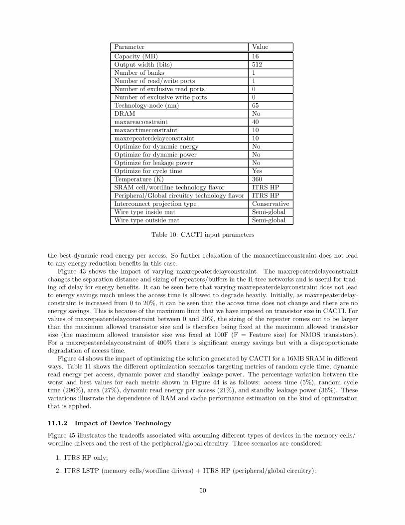
Parameter Value
Capacity (MB) 16Output width (bits) 512Number of banks 1Number of read/write ports 1Number of exclusive read ports 0Number of exclusive write ports 0Technology-node (nm) 65DRAM Nomaxareaconstraint 40maxacctimeconstraint 10maxrepeaterdelayconstraint 10Optimize for dynamic energy NoOptimize for dynamic power NoOptimize for leakage power NoOptimize for cycle time YesTemperature (K) 360SRAM cell/wordline technology flavor ITRS HPPeripheral/Global circuitry technology flavor ITRS HPInterconnect projection type ConservativeWire type inside mat Semi-globalWire type outside mat Semi-global
Table 10: CACTI input parameters
the best dynamic read energy per access. So further relaxation of the maxacctimeconstraint does not leadto any energy reduction benefits in this case.
Figure 43 shows the impact of varying maxrepeaterdelayconstraint. The maxrepeaterdelayconstraintchanges the separation distance and sizing of repeaters/buffers in the H-tree networks and is useful for trad-ing off delay for energy benefits. It can be seen here that varying maxrepeaterdelayconstraint does not leadto energy savings much unless the access time is allowed to degrade heavily. Initially, as maxrepeaterdelay-constraint is increased from 0 to 20%, it can be seen that the access time does not change and there are noenergy savings. This is because of the maximum limit that we have imposed on transistor size in CACTI. Forvalues of maxrepeaterdelayconstraint between 0 and 20%, the sizing of the repeater comes out to be largerthan the maximum allowed transistor size and is therefore being fixed at the maximum allowed transistorsize (the maximum allowed transistor size was fixed at 100F (F = Feature size) for NMOS transistors).For a maxrepeaterdelayconstraint of 400% there is significant energy savings but with a disproportionatedegradation of access time.
Figure 44 shows the impact of optimizing the solution generated by CACTI for a 16MB SRAM in differentways. Table 11 shows the different optimization scenarios targeting metrics of random cycle time, dynamicread energy per access, dynamic power and standby leakage power. The percentage variation between theworst and best values for each metric shown in Figure 44 is as follows: access time (5%), random cycletime (296%), area (27%), dynamic read energy per access (21%), and standby leakage power (36%). Thesevariations illustrate the dependence of RAM and cache performance estimation on the kind of optimizationthat is applied.
11.1.2 Impact of Device Technology
Figure 45 illustrates the tradeoffs associated with assuming different types of devices in the memory cells/-wordline drivers and the rest of the peripheral/global circuitry. Three scenarios are considered:
1. ITRS HP only;
2. ITRS LSTP (memory cells/wordline drivers) + ITRS HP (peripheral/global circuitry);
50
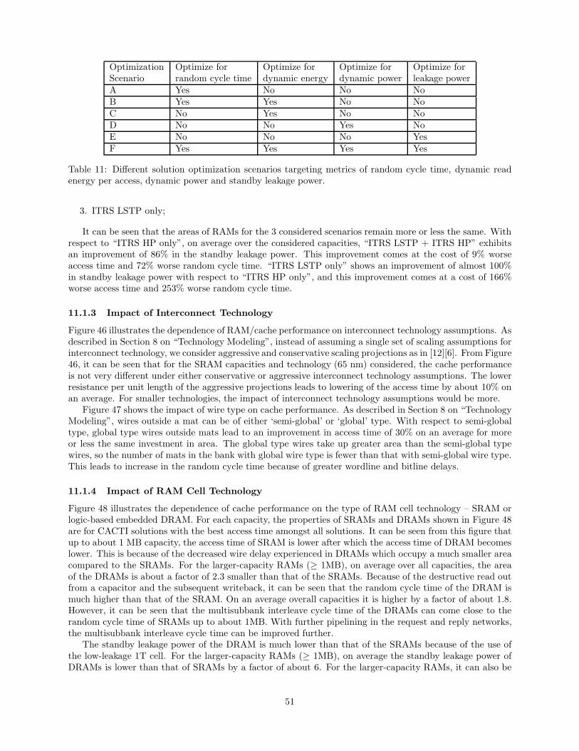
Optimization Optimize for Optimize for Optimize for Optimize forScenario random cycle time dynamic energy dynamic power leakage powerA Yes No No NoB Yes Yes No NoC No Yes No NoD No No Yes NoE No No No YesF Yes Yes Yes Yes
Table 11: Different solution optimization scenarios targeting metrics of random cycle time, dynamic readenergy per access, dynamic power and standby leakage power.
3. ITRS LSTP only;
It can be seen that the areas of RAMs for the 3 considered scenarios remain more or less the same. Withrespect to “ITRS HP only”, on average over the considered capacities, “ITRS LSTP + ITRS HP” exhibitsan improvement of 86% in the standby leakage power. This improvement comes at the cost of 9% worseaccess time and 72% worse random cycle time. “ITRS LSTP only” shows an improvement of almost 100%in standby leakage power with respect to “ITRS HP only”, and this improvement comes at a cost of 166%worse access time and 253% worse random cycle time.
11.1.3 Impact of Interconnect Technology
Figure 46 illustrates the dependence of RAM/cache performance on interconnect technology assumptions. Asdescribed in Section 8 on “Technology Modeling”, instead of assuming a single set of scaling assumptions forinterconnect technology, we consider aggressive and conservative scaling projections as in [12][6]. From Figure46, it can be seen that for the SRAM capacities and technology (65 nm) considered, the cache performanceis not very different under either conservative or aggressive interconnect technology assumptions. The lowerresistance per unit length of the aggressive projections leads to lowering of the access time by about 10% onan average. For smaller technologies, the impact of interconnect technology assumptions would be more.
Figure 47 shows the impact of wire type on cache performance. As described in Section 8 on “TechnologyModeling”, wires outside a mat can be of either ‘semi-global’ or ‘global’ type. With respect to semi-globaltype, global type wires outside mats lead to an improvement in access time of 30% on an average for moreor less the same investment in area. The global type wires take up greater area than the semi-global typewires, so the number of mats in the bank with global wire type is fewer than that with semi-global wire type.This leads to increase in the random cycle time because of greater wordline and bitline delays.
11.1.4 Impact of RAM Cell Technology
Figure 48 illustrates the dependence of cache performance on the type of RAM cell technology – SRAM orlogic-based embedded DRAM. For each capacity, the properties of SRAMs and DRAMs shown in Figure 48are for CACTI solutions with the best access time amongst all solutions. It can be seen from this figure thatup to about 1 MB capacity, the access time of SRAM is lower after which the access time of DRAM becomeslower. This is because of the decreased wire delay experienced in DRAMs which occupy a much smaller areacompared to the SRAMs. For the larger-capacity RAMs (≥ 1MB), on average over all capacities, the areaof the DRAMs is about a factor of 2.3 smaller than that of the SRAMs. Because of the destructive read outfrom a capacitor and the subsequent writeback, it can be seen that the random cycle time of the DRAM ismuch higher than that of the SRAM. On an average overall capacities it is higher by a factor of about 1.8.However, it can be seen that the multisubbank interleave cycle time of the DRAMs can come close to therandom cycle time of SRAMs up to about 1MB. With further pipelining in the request and reply networks,the multisubbank interleave cycle time can be improved further.
The standby leakage power of the DRAM is much lower than that of the SRAMs because of the use ofthe low-leakage 1T cell. For the larger-capacity RAMs (≥ 1MB), on average the standby leakage power ofDRAMs is lower than that of SRAMs by a factor of about 6. For the larger-capacity RAMs, it can also be
51

seen that the dynamic read energy per access of the DRAMs is more or less the same as that of the SRAMs.It is important to note that the comparisons presented here were for SRAMs and DRAMs with the bestaccess time amongst all solutions.
11.2 Version 4.2 vs Version 5.0 Comparisons
We first present the differences in the technology metrics of versions 4.2 and 5.0. Figure 49 shows FO4delays for versions 4.2 and 5.0. For version 5.0, the FO4 delay has been shown for the ITRS HP device type.It can be seen that, surprisingly, there is good agreement between the FO4 delays of versions 4.2 and 5.0,particularly at the 65 nm node.
Figures 50, 51 and 52 shows the trends for resistance per unit micron, capacitance per unit micron andunbuffered delay for a wire of length 1-micron for versions 4.2 and 5.0. For version 4.2, trends are shownfor both ‘local’ and ‘global’ wire types which were discussed in Section 2.3. For version 5.0, trends areshown for both ‘semi-global’ and ‘global’ wire types and for both aggressive and conservative assumptionsof interconnect technology as discussed in Section 8.2. It can be seen that the unbuffered wire delay of thelocal wire type of version 4.2 is greater than that of the semi-global wire type of version 5.0 by a factor ofabout 3.5.
Figure 53 compares results generated by CACTI version 4.2 and version 5.0. For version 5.0, we showthree solutions – solutions with best access time, best area and best dynamic read energy per access. We alsoshow results from a modified version of version 4.2. In the modified version, we increase the limits definedfor Ndwl, Ndbl, Nspd, number of subarrays and number of segments allowed in the H-trees. Increasing theseset limits allows a richer exploration of the search space of array partitions, particularly for large SRAMs.We call this version, version 4.2-limits-removed.
Because of significant modeling differences between versions 4.2 and 5.0, it is not easy to compare andanalyze the behavior of the two versions, but we make general observations and present high-level plausiblereasons for the trends. Firstly, regarding area, we observe that the areas of solutions produced by version5.0 are much greater than that of the version 4.2 solution. Version 5.0 has made a major update to the areamodel and has introduced new features such as inclusion of ECC and redundancy overheads which increasearea overhead. Also version 5.0 makes use of a bigger SRAM cell at 146F 2 compared to the 120F 2 cell usedin version 4.2. For the 32 MB SRAM, the solution generated by version 4.2-limits-removed has an area of343 mm2 which is greater than the areas of all version 5.0 solutions.
Regarding access time, it can be seen that the access times for the best access time and best dynamicenergy solutions of version 5.0 are much lower and scale in a much better way compared to the version 4.2solution. The access time of the 32 MB SRAM gets better with version 4.2-limits-removed, however, it’sstill much worse than the access time of the version 5.0 best access time and best dynamic energy solutions.The main reason for the larger access times of version 4.2 is because of the high resistance per unit lengthof the local wires in version 4.2.
Regarding dynamic energy, it can be seen that the dynamic energy per read access of the version 5.0best access time and best dynamic energy solutions are greater than that of version 4.2 by a factor of about5 on an average. This is mainly because of the organization that has been assumed in version 5.0 in whichwordlines and bitlines in multiple mats are activated per access. Also, as described in Section 2.2, bugs inversion 4.2 with respect to dynamic energy of routing in the H-trees causes the dynamic energy per readaccess to be underestimated.
Leakage power is heavily dependent on the underlying technology data. The standby leakage of version4.2 is greater than that of the best access time and best dynamic energy solutions of version 5.0 by a factorof about 3 on an average.
52

0
5
10
15
20
25
30
0 5 10 15 20 25 30 35 40 45 50
Max area percentage away from best area solution
Acc
ess
tim
e (n
s)
0
5
10
15
20
25
0 5 10 15 20 25 30 35 40 45 50
Max area percentage away from best area solution
Ran
do
m c
ycle
tim
e (n
s)
0
50
100
150
200
250
0 5 10 15 20 25 30 35 40 45 50
Max area percentage away from best area solution
Are
a (m
m2)
0
2
4
6
8
10
12
0 5 10 15 20 25 30 35 40 45 50
Max area percentage away from best area solution
Dyn
amic
rea
d e
ner
gy
per
acc
ess
(nJ)
0
5000
10000
15000
20000
25000
30000
0 5 10 15 20 25 30 35 40 45 50
Max area percentage away from best area solution
Sta
nd
by
leak
age
po
wer
per
ban
k (m
W)
0
20
40
60
80
100
120
140
0 5 10 15 20 25 30 35 40 45 50
Max area percentage away from best area solution
Nd
wl,
Nd
bl a
nd
Nsp
d
Ndwl
Ndbl
Nspd
Figure 41: Access time, random cycle time, area, dynamic energy and leakage power of a 16MB SRAM asmaxareaconstraint is varied.
53

0
1
2
3
4
5
6
7
8
9
0 5 10 15 20 25 30 35 40 45 50
Max delay percentage away from best delay solution
Acc
ess
tim
e (n
s)
0
0.2
0.4
0.6
0.8
1
1.2
0 5 10 15 20 25 30 35 40 45 50
Max delay percentage away from best delay solution
Ran
do
m c
ycle
tim
e (n
s)
0
20
40
60
80
100
120
140
160
180
200
0 5 10 15 20 25 30 35 40 45 50
Max delay percentage away from best delay solution
Are
a (m
m2)
0
0.5
1
1.5
2
2.5
3
3.5
4
4.5
5
0 5 10 15 20 25 30 35 40 45 50
Max delay percentage away from best delay solution
Dyn
amic
rea
d e
ner
gy
per
acc
ess
(nJ)
0
5000
10000
15000
20000
25000
30000
0 5 10 15 20 25 30 35 40 45 50
Max delay percentage away from best delay solution
Sta
nd
by
leak
age
po
wer
per
ban
k (m
W)
Figure 42: Access time, random cycle time, area, dynamic energy and leakage power of a 16MB SRAM asmaxacctimeconstraint is varied.
54

0
5
10
15
20
25
0 10 20 30 40 50 60 70 80 90 100 200 400 800
Max percentage difference from best delay repeater
Acc
ess
tim
e (n
s)
0
0.5
1
1.5
2
2.5
3
3.5
0 10 20 30 40 50 60 70 80 90 100 200 400 800
Max percentage difference from best delay repeater
Ran
do
m c
ycle
tim
e (n
s)
0
20
40
60
80
100
120
140
160
180
0 10 20 30 40 50 60 70 80 90 100 200 400 800
Max percentage difference from best delay repeater
Are
a (m
m2)
0
0.5
1
1.5
2
2.5
3
3.5
4
0 10 20 30 40 50 60 70 80 90 100 200 400 800
Max percentage difference from best delay repeater
Dyn
amic
rea
d e
ner
gy
per
acc
ess
(nJ)
0
5000
10000
15000
20000
25000
30000
0 10 20 30 40 50 60 70 80 90 100 200 400 800
Max percentage difference from best delay repeater
Sta
nd
by
leak
age
po
wer
per
ban
k (m
W)
Figure 43: Access time, random cycle time, area, dynamic energy and leakage power of a 16MB SRAM asmaxrepeaterdelayconstraint is varied.
55

0
1
2
3
4
5
6
7
8
A B C D E F
Optimization scenarios
Acc
ess
tim
e (n
s)
0
0.5
1
1.5
2
2.5
A B C D E F
Optimization scenarios
Ran
do
m c
ycle
tim
e (n
s)
0
20
40
60
80
100
120
140
160
180
A B C D E F
Optimization scenarios
Are
a (m
m2)
0
0.5
1
1.5
2
2.5
3
3.5
A B C D E F
Optimization scenarios
Dyn
amic
rea
d e
ner
gy
per
acc
ess
(nJ)
0
5000
10000
15000
20000
25000
30000
A B C D E F
Optimization scenarios
Sta
nd
by
leak
age
po
wer
per
ban
k (m
W)
Figure 44: Access time, random cycle time, area, dynamic energy and leakage power of a 16MB SRAMunder different optimization function scenarios.
56

0
5
10
15
20
25
30
1 2 4 8 16 32
Capacity (MB)
Acc
ess
tim
e (n
s)
ITRS HP in mem cell and periph-global
ITRS LSTP in mem cell, ITRS HP in periph-global
ITRS LSTP in mem cell and periph-global
0
0.5
1
1.5
2
2.5
1 2 4 8 16 32
Capacity (MB)
Ran
do
m c
ycle
tim
e (n
s)
ITRS HP in mem cell and periph-global
ITRS LSTP in mem cell, ITRS HP in periph-global
ITRS LSTP in mem cell and periph-global
0
50
100
150
200
250
300
350
400
1 2 4 8 16 32
Capacity (MB)
Are
a (m
m2)
ITRS HP in mem cell and periph-global
ITRS LSTP in mem cell, ITRS HP in periph-global
ITRS LSTP in mem cell and periph-global
0
1
2
3
4
5
6
7
8
1 2 4 8 16 32
Capacity (MB)
Dyn
amic
rea
d e
ner
gy
per
acc
ess
(nJ)
ITRS HP in mem cell and periph-global
ITRS LSTP in mem cell, ITRS HP in periph-global
ITRS LSTP in mem cell and periph-global
1 2 4 8 16 32
0 5000
10000
15000
20000
25000
30000
35000
40000
45000
50000
Sta
nd
by
leak
age
po
wer
per
ban
k
(mW
)
Capacity (MB)
ITRS HP in mem cell and periph-global
ITRS LSTP in mem cell, ITRS HP in periph-global
ITRS LSTP in mem cell and periph-global
Figure 45: Access time, random cycle time, area, dynamic energy and leakage power of SRAMs for different65 nm device technology assumptions.
57

0
2
4
6
8
10
12
1 2 4 8 16 32
Capacity (MB)
Acc
ess
tim
e (n
s)
Conservative interconnect projections
Aggressive interconnect projections
0
0.1
0.2
0.3
0.4
0.5
0.6
0.7
0.8
0.9
1
1 2 4 8 16 32
Capacity (MB)
Ran
do
m c
ycle
tim
e (n
s)
Conservative interconnect projections
Aggressive interconnect projections
0
50
100
150
200
250
300
350
400
1 2 4 8 16 32
Capacity (MB)
Are
a (m
m2)
Conservative interconnect projections
Aggressive interconnect projections
0
0.5
1
1.5
2
2.5
3
3.5
4
4.5
5
1 2 4 8 16 32
Capacity (MB)
Dyn
amic
rea
d e
ner
gy
per
acc
ess
(nJ)
Conservative interconnect projections
Aggressive interconnect projections
0
10000
20000
30000
40000
50000
60000
1 2 4 8 16 32
Capacity (MB)
Sta
nd
by
leak
age
po
wer
(m
W)
Conservative interconnect projections
Aggressive interconnect projections
Figure 46: Access time, random cycle time, area, dynamic energy and leakage power of SRAMs underaggressive and conservative interconnect technology assumptions.
58

0
2
4
6
8
10
12
1 2 4 8 16 32
Capacity (MB)
Acc
ess
tim
e (n
s)
Semi-global type wires outside mat
Global type wires outside mat
0
0.1
0.2
0.3
0.4
0.5
0.6
0.7
0.8
1 2 4 8 16 32
Capacity (MB)
Ran
do
m c
ycle
tim
e (n
s)
Semi-global type wires outside mat
Global type wires outside mat
0
50
100
150
200
250
300
350
400
1 2 4 8 16 32
Capacity (MB)
Are
a (m
m2)
Semi-global type wires outside mat
Global type wires outside mat
0
0.5
1
1.5
2
2.5
3
3.5
4
4.5
5
1 2 4 8 16 32
Capacity (MB)
Dyn
amic
rea
d e
ner
gy
per
acc
ess
(nJ)
Semi-global type wires outside mat
Global type wires outside mat
0
10000
20000
30000
40000
50000
60000
1 2 4 8 16 32
Capacity (MB)
Sta
nd
by
leak
age
po
wer
(m
W)
Semi-global type wires outside mat
Global type wires outside mat
Figure 47: Access time, random cycle time, area, dynamic energy and leakage power of SRAMs with “global”interconnect type used for wires outside the mat.
59

0
1
2
3
4
5
6
7
8
9
10
8K
16K
32K
64K
128K
256K
512K
1M
2M
4M
8M
16
M
32M
Capacity (bytes)
Acc
ess
tim
e (n
s)
SRAM
DRAM
0
0.5
1
1.5
2
2.5
3
8K
16K
32K
64K
128K
256K
512K
1M
2M
4M
8M
16M
32M
Capacity (bytes)
Cyc
le t
ime
(ns)
SRAM random
DRAM random
DRAM multisubbank interleave
0
0.5
1
1.5
2
2.5
3
3.5
4
8K 16K 32K 64K 128K 256K 512K
Capacity (bytes)
Are
a (m
m2)
SRAM
DRAM
0
50
100
150
200
250
300
1M 2M 4M 8M 16M 32M
Capacity (bytes)
Are
a (m
m2)
SRAM
DRAM
0
0.05
0.1
0.15
0.2
0.25
8K 16K 32K 64K 128K 256K 512K
Capacity (bytes)
Dyn
rea
d e
ner
gy
per
rea
d a
cces
s
(nJ)
SRAM
DRAM
0
1
2
3
4
5
6
1M 2M 4M 8M 16M 32M
Capacity (bytes)
Dyn
rea
d e
ner
gy
per
rea
d a
cces
s
(nJ)
SRAM
DRAM
0
100
200
300
400
500
600
700
800
8K 16K 32K 64K 128K 256K 512K
Capacity (bytes)
Sta
nd
by
leak
age
po
wer
(m
W) SRAM
DRAM
0
5000
10000
15000
20000
25000
30000
35000
40000
45000
50000
1M 2M 4M 8M 16M 32M
Capacity (bytes)
Sta
nd
by
leak
age
po
wer
(m
W) SRAM
DRAM
Figure 48: Access time, cycle time, area, dynamic read energy per access and standby leakage power ofSRAM and logic-based embedded DRAM for 65 nm technology. The area, dynamic read energy per accessand standby leakage power trends are split up into two charts based on capacities.
60

0
2
4
6
8
10
12
14
16
18
20
90 65 45 32
Technology node (nm)
FO
4 d
elay
(p
s)
v4.2
v5.0
Figure 49: FO4 delays for various technology nodes in versions 4.2 and 5.0. The version 5.0 FO4 delays arefor ITRS high-performance device type.
0
2
4
6
8
10
12
14
16
18
90 65 45 32
Technology node (nm)
Res
ista
nce
per
un
it m
icro
n
(oh
m/m
icro
n)
v4.2 local
v4.2 global
v5.0 semi-global cons
v5.0 semi-global aggr
v5.0 global cons
v5.0 global aggr
Figure 50: Resistance per unit micron of wire at various technology nodes for versions 4.2 and 5.0.
61

0
0.05
0.1
0.15
0.2
0.25
0.3
0.35
0.4
90 65 45 32
Technology node (nm)
Cap
acit
ance
per
un
it m
icro
n
(fF
/mic
ron
)
v4.2 local
v4.2 global
v5.0 semi-global cons
v5.0 semi-global aggr
v5.0 global cons
v5.0 global aggr
Figure 51: Capacitance per unit micron of wire at various technology nodes for versions 4.2 and 5.0.
0
0.0002
0.0004
0.0006
0.0008
0.001
0.0012
0.0014
0.0016
90 65 45 32
Technology node (nm)
Un
bu
ffer
ed w
ire
del
ay f
or
1-m
icro
n
len
gth
wir
e (p
s)
v4.2 local
v4.2 global
v5.0 semi-global cons
v5.0 semi-global aggr
v5.0 global cons
v5.0 global aggr
Figure 52: Unbuffered delays through a wire of length 1-micron for various technology nodes in versions 4.2and 5.0. The wire delays for version 5.0 are for both aggressive and conservative projections.
62

0
5
10
15
20
25
30
35
40
45
50
1 2 4 8 16 32
Capacity (MB)
Acc
ess
tim
e (n
s)
v4.2
v4.2-limits-removed
v5.0-best-acc-time
v5.0-best-area
v5.0-best-dyn-energy
0
10
20
30
40
50
60
1 2 4 8 16 32
Capacity (MB)
Ran
do
m c
ycle
tim
e (n
s)
v4.2
v4.2-limits-removed
v5.0-best-acc-time
v5.0-best-area
v5.0-best-dyn-energy
0
50
100
150
200
250
300
350
400
1 2 4 8 16 32
Capacity (MB)
Are
a (m
m2)
v4.2
v4.2-limits removed
v5.0-best-acc-time
v5.0-best-area
v5.0-best-dyn-energy
0
5
10
15
20
25
1 2 4 8 16 32
Capacity (MB)
Dyn
amic
rea
d e
ner
gy
per
acc
ess
(nJ)
v4.2
v4.2-limits-removed
v5.0-best-acc-time
v5.0-best-area
v5.0-best-dyn-energy
0
20000
40000
60000
80000
100000
120000
1 2 4 8 16 32
Capacity (MB)
Sta
nd
by
leak
age
po
wer
(m
W)
v4.2
v4.2-limits-removed
v5.0-best-acc-time
v5.0-best-area
v5.0-best-dyn-energy
Figure 53: Access time, random cycle time, area, dynamic energy and leakage power obtained from versions4.2 and 5.0 for SRAMs in 70 nm technology.
63
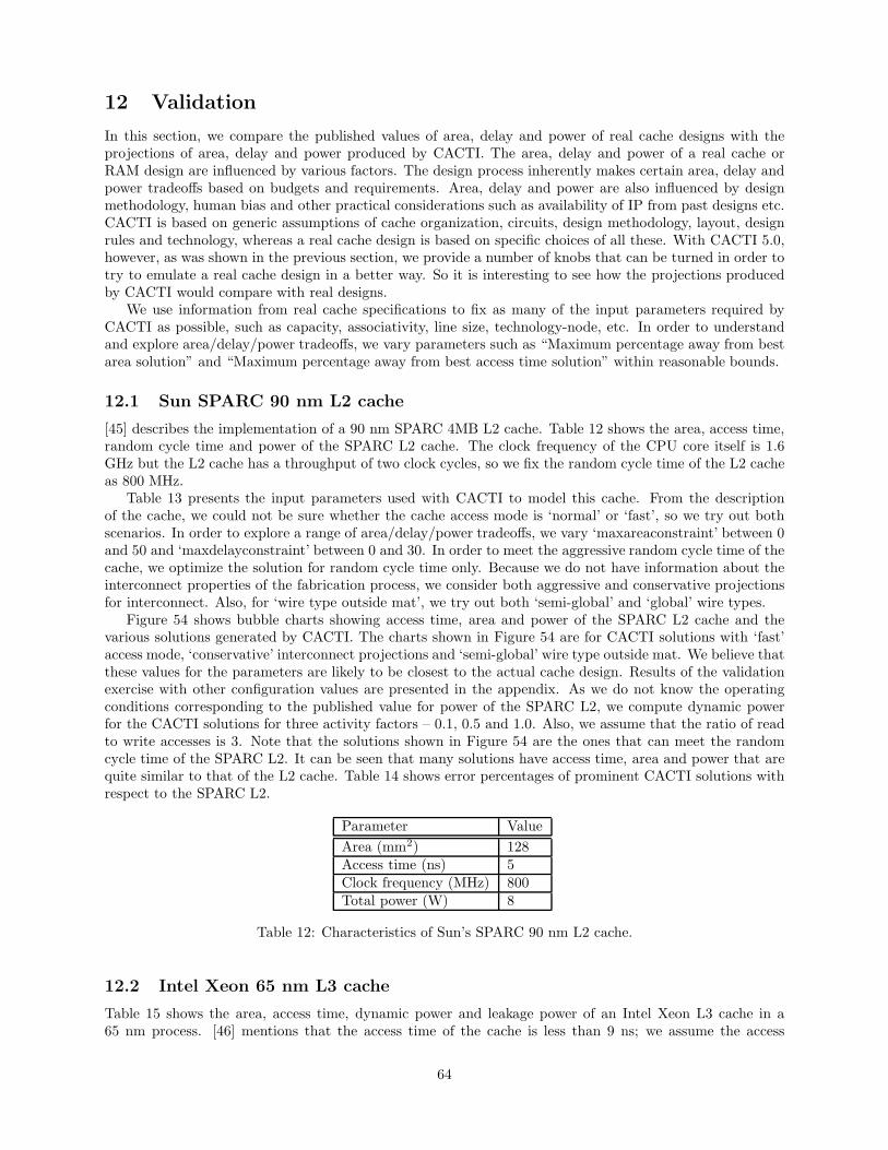
12 Validation
In this section, we compare the published values of area, delay and power of real cache designs with theprojections of area, delay and power produced by CACTI. The area, delay and power of a real cache orRAM design are influenced by various factors. The design process inherently makes certain area, delay andpower tradeoffs based on budgets and requirements. Area, delay and power are also influenced by designmethodology, human bias and other practical considerations such as availability of IP from past designs etc.CACTI is based on generic assumptions of cache organization, circuits, design methodology, layout, designrules and technology, whereas a real cache design is based on specific choices of all these. With CACTI 5.0,however, as was shown in the previous section, we provide a number of knobs that can be turned in order totry to emulate a real cache design in a better way. So it is interesting to see how the projections producedby CACTI would compare with real designs.
We use information from real cache specifications to fix as many of the input parameters required byCACTI as possible, such as capacity, associativity, line size, technology-node, etc. In order to understandand explore area/delay/power tradeoffs, we vary parameters such as “Maximum percentage away from bestarea solution” and “Maximum percentage away from best access time solution” within reasonable bounds.
12.1 Sun SPARC 90 nm L2 cache
[45] describes the implementation of a 90 nm SPARC 4MB L2 cache. Table 12 shows the area, access time,random cycle time and power of the SPARC L2 cache. The clock frequency of the CPU core itself is 1.6GHz but the L2 cache has a throughput of two clock cycles, so we fix the random cycle time of the L2 cacheas 800 MHz.
Table 13 presents the input parameters used with CACTI to model this cache. From the descriptionof the cache, we could not be sure whether the cache access mode is ‘normal’ or ‘fast’, so we try out bothscenarios. In order to explore a range of area/delay/power tradeoffs, we vary ‘maxareaconstraint’ between 0and 50 and ‘maxdelayconstraint’ between 0 and 30. In order to meet the aggressive random cycle time of thecache, we optimize the solution for random cycle time only. Because we do not have information about theinterconnect properties of the fabrication process, we consider both aggressive and conservative projectionsfor interconnect. Also, for ‘wire type outside mat’, we try out both ‘semi-global’ and ‘global’ wire types.
Figure 54 shows bubble charts showing access time, area and power of the SPARC L2 cache and thevarious solutions generated by CACTI. The charts shown in Figure 54 are for CACTI solutions with ‘fast’access mode, ‘conservative’ interconnect projections and ‘semi-global’ wire type outside mat. We believe thatthese values for the parameters are likely to be closest to the actual cache design. Results of the validationexercise with other configuration values are presented in the appendix. As we do not know the operatingconditions corresponding to the published value for power of the SPARC L2, we compute dynamic powerfor the CACTI solutions for three activity factors – 0.1, 0.5 and 1.0. Also, we assume that the ratio of readto write accesses is 3. Note that the solutions shown in Figure 54 are the ones that can meet the randomcycle time of the SPARC L2. It can be seen that many solutions have access time, area and power that arequite similar to that of the L2 cache. Table 14 shows error percentages of prominent CACTI solutions withrespect to the SPARC L2.
Parameter Value
Area (mm2) 128Access time (ns) 5Clock frequency (MHz) 800Total power (W) 8
Table 12: Characteristics of Sun’s SPARC 90 nm L2 cache.
12.2 Intel Xeon 65 nm L3 cache
Table 15 shows the area, access time, dynamic power and leakage power of an Intel Xeon L3 cache in a65 nm process. [46] mentions that the access time of the cache is less than 9 ns; we assume the access
64

Parameter Value
Capacity (MB) 4Line size (bytes) 32Associativity 4Number of read/write ports 1Number of exclusive ports 0Number of banks 1Technology-node (nm) 90Output width (bits) 256Specific tag YesTag width 34Access mode Normal/FastPure RAM No (cache)DRAM NoRepeaters in bank H-trees Yesmaxareaconstraint 0 - 70maxacctimeconstraint 0 - 30maxrepeaterdelayconstraint 10Optimize for dynamic energy NoOptimize for dynamic power NoOptimize for leakage power NoOptimize for cycle time YesTemperature (K) 360SRAM cell/wordline technology flavor ITRS HPPeripheral/Global circuitry technology flavor ITRS HPInterconnect projection type ConservativeWire type inside mat Semi-globalWire type outside mat Semi-global/Global
Table 13: CACTI input parameters used for modeling 90 nm SPARC L2 cache
time to be 9 ns. The clock frequency of the core itself is given to be 3.4 GHz and the clock frequency ofthe L3 is given to be half that of the core [47]. Also, because the output bus width of the L3 is 256 bits,it would require two cycles to transmit a 64-byte line, so we fix the random cycle frequency of the L3 tobe one-fourth that of the CPU, i.e. 850 MHz. The dynamic power of the cache comes out to be 5.4Wbased on information from [47][48], however [21] mentions that the cache consumes about 1.7W for “averageapplications”. We speculate that these differences in dynamic power numbers that have been quoted arebecause of different activity factors in the cache caused due to measurements or simulations of applicationswith different characteristics. While carrying out comparisons of the area, delay and power of the Intel cachewith those of the solutions generated by CACTI, we use both values of power.
The 65 nm process offers transistors with 35 nm gate-lengths. The cache itself, however, makes use oflonger-channel devices with lengths that are about 10% longer than the nominal. The longer-channel deviceshave on-currents that are about 10% less than the nominal devices but have leakage that is lower by a factorof 3. The cache operates in a voltage domain different from that of the cores. The cores can operate at1.25V while the cache operates at 1.1V.
In order to control leakage in the cache, the Intel cache implements n and p sleep transistors at the levelof ‘blocks’ within subarrays (Each subarray within the Intel cache is composed of multiple ‘blocks’ with oneblock within a subarray activated per access. The ‘subarray’ of the Intel cache is not the same as that ofCACTI). The impact of these sleep transistors is that leakage power in all blocks that are not activatedduring an access is cut down by half.
Table 16 shows the input parameters used with CACTI to model the Intel L3 cache. In order to comparethe power numbers produced by CACTI with those of the Intel cache in a fair manner, we assume the use
65

Activity factor for dynamic power = 0.1
0
1
2
3
4
5
6
7
0 5 10 15 Power (W)
Acc
ess
tim
e (n
s)
CACTI generated solutions
Target SPARC L2
Activity factor for dynamic power = 0.5
0
1
2
3
4
5
6
7
0 5 10 15 Power (W)
Acc
ess
tim
e (n
s)
CACTI generated solutions
Target SPARC L2
Activity factor for dynamic power = 1.0
0
1
2
3
4
5
6
7
0 5 10 15 Power (W)
Acc
ess
tim
e (n
s)
CACTI generated solutions
Target SPARC L2
Figure 54: Access time, area and power of the 90 nm SPARC L2 cache and of solutions generated by CACTI.The CACTI solutions assume ‘fast’ access mode, ‘conservative’ interconnect projections and ‘semi-global’wire type outside mat. The 3 plots correspond to 3 activity factors assumed while computing dynamic powerfor the CACTI-generated solutions.
of leakage control mechanisms within CACTI similar to that used in the Intel cache. To model the longer-channel devices that have been used in the Intel cache which reduce leakage by a factor of 3, we also reducethe leakage of the CACTI 65 nm high-performance transistors by a factor of 3. Also, we assume the use ofsleep transistors that cut down the leakage of all mats that are not activated during an access by half.
Figure 55 shows bubble charts of access time, area, and power of the Intel cache and the various solutionsgenerated by CACTI. The charts shown in Figure 55 are for CACTI solutions with ‘conservative’ interconnectprojections and ‘semi-global’ wire type outside mat as we believe that these values for the parameters arelikely to be closest to the actual cache design. Results of the validation exercise with other configurationvalues are again presented in the appendix. Again, as we do not know the operating conditions correspondingto the published value for power, we compute dynamic power for the CACTI solutions for three activityfactors – 0.1, 0.5 and 1.0. Again, we assume that the ratio of read to write accesses is 3. There are twotargets for the Intel cache corresponding to the two values of dynamic power shown in Table 15. It can beseen from Figure 55 that many CACTI solutions have area, access time and power that are quite similar tothat of the Xeon L3. Tables 17 and 18 show error percentages of prominent CACTI solutions with respectto the Xeon L3.
66

Solution % error in % error in % error in Avg of acc time, areaacc time area power and power % errors
Best % error inacc time 0/0/0 -3/-3/-3 -67/-52/-33 23/18/12Best % error inarea 0/0/0 -3/-3/-3 -67/-52/-33 23/18/12Best % error inpower 0/0/0 -3/-3/-3 -67/-52/-33 23/18/12Best average ofarea, acc time andpower % errors 0/0/0 -3/-3/-3 -67/-52/-33 23/18/12Best average ofarea and acc time 0/0/0 -3/-3/-3 -67/-52/-33 23/18/12% errorsBest average ofacc time and power 0/0/5 20/20/49 -63/-44/-14 28/22/23% errorsBest acc time 0/0/0 -3/-3/-3 -67/-52/-33 23/18/12Best area 0/0/0 -3/-3/-3 -67/-52/-33 23/18/12Best power 0/0/0 -3/-3/-3 -67/-52/-33 23/18/12
Table 14: Error percentages of some prominent solutions generated by CACTI with respect to a 90 nmSPARC L2 cache. The CACTI solutions assume ‘fast’ access mode, ‘conservative’ interconnect projectionsand ‘semi-global’ wire type outside mat. We have used 3 activity factors of 0.1, 0.5 and 1, and so each entryin the table has 3 values.
Area (mm2) 200 Measured from die photo [49]Access time (ns) 9 ns [46]Clock frequency (GHz) 850 MHz [47]Dynamic power (W) 1.7/5.4 [47][48][21]Leakage power (W) 6.6 [47][48]
Table 15: Characteristics of Intel Xeon’s 65 nm L3 cache.
67

Parameter Value
Capacity (MB) 16Line size (bytes) 64Associativity 16Number of read/write ports 1Number of exclusive ports 0Number of banks 2Technology-node (nm) 65Output width (bits) 512Specific tag NoAccess mode SerialPure RAM No (cache)DRAM Nomaxareaconstraint 0 - 50maxdelayconstraint 0 - 30maxrepeaterdelayconstraint 10Optimize for dynamic energy NoOptimize for dynamic power NoOptimize for leakage power NoOptimize for cycle time YesTemperature (K) 360SRAM cell/wordline technology flavor ITRS HPPeripheral/Global circuitry technology flavor ITRS HPInterconnect projection type ConservativeWire type inside mat Semi-globalWire type outside mat Semi-global/Global
Table 16: CACTI input parameters used for modeling 65 nm Intel Xeon L3 cache.
68

Activity factor for dynamic power = 0.1
0
2
4
6
8
10
12
14
0 5 10 15 20 25 30 Power (W)
Acc
ess
tim
e (n
s)
CACTI generated solutions
Target Intel L3; dyn pow = 1.7W
Target Intel L3; dyn pow = 5.4W
Activity factor for dynamic power = 0.5
0
2
4
6
8
10
12
14
0 5 10 15 20 25 30
Power (W)
Acc
ess
tim
e (n
s)
CACTI generated solutions
Target Intel L3; dyn pow = 1.7W
Target Intel L3; dyn pow = 5.4W
Activity factor for dynamic power = 1.0
0
2
4
6
8
10
12
14
0 5 10 15 20 25 30
Power (W)
Acc
ess
tim
e (n
s)
CACTI generated solutions
Target Intel L3; dyn pow = 1.7W
Target Intel L3; dyn pow = 5.4W
Figure 55: Access time, area and power of the 65 nm Xeon L3 cache and of solutions generated by CACTI.The CACTI solutions assume ‘conservative’ interconnect projections and ‘semi-global’ wire type outsidemat. The 3 plots correspond to 3 activity factors assumed while computing dynamic power for the CACTI-generated solutions.
69

Solution % error in % error in % error in Avg of acc time, areaacc time area power and power % errors
Best % error inacc time -11/-11/-11 -23/-23/-23 -40/-19/7 24/18/14Best % error inarea -11/-11/-11 -23/-23/-23 -40/-19/7 24/18/14Best % error inpower -11/-11/-11 -23/-23/-23 -40/-19/7 24/18/14Best average ofarea, acc time andpower % errors 2/2/2 0/6/0 -31/0/21 11/3/8Best average ofarea and acc time 2/2/2 0/0/0 -31/-8/21 11/4/8% errorsBest average ofacc time and power 2/2/-4 6/6/-14 -27/0/10 12/3/9% errorsBest acc time -11/-11/-11 -23/-23/-23 -40/-19/7 24/18/14Best area -11/-11/-11 -23/-23/-23 -40/-19/7 24/18/14Best power -11/-11/-11 -23/-23/-23 -40/-19/7 24/18/14
Table 17: Error percentages of some prominent solutions generated by CACTI with respect to a 65 nmIntel Xeon L3 cache when we assume that the dynamic power consumed by the cache is 1.7W. The CACTIsolutions assume ‘conservative’ interconnect projections and ‘semi-global’ wire type outside mat. We haveused 3 activity factors of 0.1, 0.5 and 1, and so each entry in the table has 3 values.
Solution % error in % error in % error in Avg of acc time, areaacc time area power and power % errors
Best % error inacc time -11/-11/-11 -23/-23/-23 -58/-44/-26 31/26/20Best % error inarea -11/-11/-11 -23/-23/-23 -58/-44/-26 31/26/20Best % error inpower -11/-11/-11 -23/-23/-23 -58/-44/-26 31/26/20Best average ofarea, acc time andpower % errors 2/2/2 0/6/6 -52/-31/-7 18/13/5Best average ofarea and acc time 2/2/2 0/0/0 -52/-37/-17 18/13/6% errorsBest average ofacc time and power 2/2/2 6/6/6 -49/-31/-7 19/13/5% errorsBest acc time -11/-11/-11 -23/-23/-23 -58/-44/-26 31/26/20Best area -11/-11/-11 -23/-23/-23 -58/-44/-26 31/26/20Best power -11/-11/-11 -23/-23/-23 -58/-44/-26 31/26/20
Table 18: Error percentages of some prominent solutions generated by CACTI with respect to a 65 nmIntel Xeon L3 cache when we assume that the dynamic power consumed by the cache is 5.4W. The CACTIsolutions assume ‘conservative’ interconnect projections and ‘semi-global’ wire type outside mat. We haveused 3 activity factors of 0.1, 0.5 and 1, and so each entry in the table has 3 values.
70

13 Future Work
Non Uniform Cache Access (NUCA) is an interesting architecture that CACTI could support in the future.Incorporation of models for low-swing interconnect into CACTI could also be an interesting enhancement.
14 Conclusions
In this technical report, we have described the various enhancements carried out in CACTI 5.0 while alsoproviding a comprehensive overview of the CACTI area, access time and power modeling. CACTI 5.0includes a number of major improvements over CACTI 4.0. The base technology modeling has been changedfrom simple linear scaling of the original 0.8 micron technology to models based on the ITRS roadmap. Datafor different ITRS device types has been incorporated into CACTI. Interconnect technology data has alsobeen updated so that it is now based off well-documented models and data. CACTI 5.0 has also addedsupport for modeling embedded DRAM in such a way that it now becomes possible to compare tradeoffsinvolving the use of embedded SRAM or DRAM for identical input specifications. This has been achievedby an extensive rewrite of the CACTI code base. Various organizational and circuit assumptions have beenclarified and updated. The modeling has also been restructured in such a way that it is now more modularand easier to extend and evolve.
In the studies shown in this report, the impact of technology assumptions on cache performance has beenpointed out and emphasized. The importance of solution optimization techniques on memory and cacheperformance has also been highlighted. Area, delay and power results obtained from version 5.0 have beencompared against published data available for two prominent caches. Taking into account the extremelygeneric nature of CACTI, it was found that there is reasonable agreement between the results produced byCACTI and the published data.
Finally, as in the original CACTI report, we would like to caution users against making too manyconclusions based on results shown in this report. It is important to know that CACTI is a simplified modelfor memories and caches with various limitations at the various levels of modeling, so appropriate cautionand judgement needs to be exercised with its use. In general, it is best to use CACTI for studies that involverelative optimization.
Acknowledgments
We would like to thank the following people for many helpful discussions and comments: Jung Ho Ahn andAl Davis from HP Labs, and Jay Brockman and Christian Poellabauer from the University of Notre Dame.
71

APPENDIX
A Additional CACTI Validation Results for 90 nm SPARC L2
Activity factor for dynamic power = 0.1
0
1 2
3 4
5
6 7
8 9
10
0 5 10 15 Power (W)
Acc
ess
tim
e (n
s)
CACTI generated solutions
Target SPARC L2
Activity factor for dynamic power = 0.5
0
1 2 3
4
5 6 7
8 9
10
0 5 10 15 Power (W)
Acc
ess
tim
e (n
s)
CACTI generated solutions
Target SPARC L2
Activity factor for dynamic power = 1.0
0
1
2
3
4 5 6
7
8
9 10
0 5 10 15 Power (W)
Acc
ess
tim
e (n
s)
CACTI generated solutions
Target SPARC L2
Figure 56: Access time, area and power of the 90 nm SPARC L2 cache and of solutions generated by CACTI.The CACTI solutions are for assumptions of ‘fast’ access mode, ‘conservative’ interconnect projections and‘global’ wire type outside mat. The 3 plots correspond to 3 activity factors assumed while computing dynamicpower for the CACTI-generated solutions.
72

Solution % error in % error in % error in Avg of acc time, areaacc time area power and power % errors
Best % error inacc time -15/-15/-15 45/45/45 -68/-54/-36 43/38/32Best % error inarea -15/-15/-15 45/45/45 -68/-54/-36 43/38/32Best % error inpower -15/-15/-15 45/45/45 -68/-54/-36 43/38/32Best average ofarea, acc time andpower % errors -15/-15/-15 45/45/45 -68/-54/-36 43/38/32Best average ofarea and acc time -15/-15/-15 45/45/45 -68/-54/-36 43/38/32% errorsBest average ofacc time and power -15/-15/-15 45/45/45 -68/-54/-36 43/38/32% errorsBest acc time -15/-15/-15 45/45/45 -68/-54/-36 43/38/32Best area -15/-15/-15 45/45/45 -68/-54/-36 43/38/32Best power -15/-15/-15 45/45/45 -68/-54/-36 43/38/32
Table 19: Error percentages of some prominent solutions generated by CACTI with respect to a 90 nmSPARC L2 cache under assumptions of ‘fast’ access mode, ‘conservative’ interconnect projections and ‘global’wire type outside mat. We have used 3 activity factors of 0.1, 0.5 and 1, and so each entry in the table has3 values.
73

Activity factor for dynamic power = 0.1
0
1 2
3 4
5
6 7
8 9
10
0 5 10 15 Power (W)
Acc
ess
tim
e (n
s)
CACTI generated solutions
Target SPARC L2
Activity factor for dynamic power = 0.5
0
1 2 3
4
5 6 7
8 9
10
0 5 10 15 Power (W)
Acc
ess
tim
e (n
s)
CACTI generated solutions
Target SPARC L2
Activity factor for dynamic power = 1.0
0
1
2
3
4 5 6
7
8
9 10
0 5 10 15 Power (W)
Acc
ess
tim
e (n
s)
CACTI generated solutions
Target SPARC L2
Figure 57: Access time, area and power of the 90 nm SPARC L2 cache and of solutions generated byCACTI. The CACTI solutions are for assumptions of ‘normal’ access mode, ‘conservative’ interconnectprojections and ‘semi-global’ wire type outside mat. The 3 plots correspond to 3 activity factors assumedwhile computing dynamic power for the CACTI-generated solutions.
74

Activity factor for dynamic power = 0.1
0
1 2
3 4
5
6 7
8 9
10
0 5 10 15 Power (W)
Acc
ess
tim
e (n
s)
CACTI generated solutions
Target SPARC L2
Activity factor for dynamic power = 0.5
0
1 2 3
4
5 6 7
8 9
10
0 5 10 15 Power (W)
Acc
ess
tim
e (n
s)
CACTI generated solutions
Target SPARC L2
Activity factor for dynamic power = 1.0
0
1
2
3
4 5 6
7
8
9 10
0 5 10 15 Power (W)
Acc
ess
tim
e (n
s)
CACTI generated solutions
Target SPARC L2
Figure 58: Access time, area and power of the 90 nm SPARC L2 cache and of solutions generated by CACTI.The CACTI solutions are for assumptions of ‘normal’ access mode, ‘conservative’ interconnect projectionsand ‘global’ wire type outside mat. The 3 plots correspond to 3 activity factors assumed while computingdynamic power for the CACTI-generated solutions.
75

Solution % error in % error in % error in Avg of acc time, areaacc time area power and power % errors
Best % error inacc time 35/35/35 -38/-38/-38 -69/-63/-54 47/45/42Best % error inarea 44/44/44 -41/-41/-41 -70/-62/-52 52/49/46Best % error inpower 44/35/35 -41/-38/-38 -70/-63/-54 52/45/42Best average ofarea, acc time andpower % errors 48/48/48 -19/-19/-19 -69/-57/-43 45/42/37Best average ofarea and acc time 48/48/48 -19/-19/-19 -69/-57/-43 45/42/37% errorsBest average ofacc time and power 37/37/37 -32/-32/-32 -67/-58/-47 46/43/39% errorsBest acc time 35/35/35 -38/-38/-38 -69/-63/-54 47/45/42Best area 44/44/44 -41/-41/-41 -70/-62/-52 52/49/46Best power 44/35/35 -41/-38/-38 -70/-63/-54 52/45/42
Table 20: Error percentages of some prominent solutions generated by CACTI with respect to a 90 nmSPARC L2 cache for a normal cache under assumptions of ‘normal’ access mode, ‘conservative’ interconnectprojections and ‘semi-global’ wire type outside mat. The CACTI solutions and errors depends on the activityfactor. We have used 3 activity factors of 0.1, 0.5 and 1, and so each entry in the table has 3 values.
Solution % error in % error in % error in Avg of acc time, areaacc time area power and power % errors
Best % error inacc time 8/8/8 -31/-31/-31 -71/-65/-58 37/35/32Best % error inarea 16/16/16 -35/-35/-35 -70/-63/-53 40/38/34Best % error inpower 8/11/11 -31/-24/-24 -71/-65/-59 37/33/31Best average ofarea, acc time andpower % errors 20/20/11 -8/-8/-20 -68/-62/-49 32/30/27Best average ofarea and acc time 20/20/20 -8/-8/-8 -68/-62/-54 32/30/27% errorsBest average ofacc time and power 8/11/11 -31/-20/-20 -71/-60/-49 37/30/27% errorsBest acc time 8/8/8 -31/-31/-31 -71/-65/-58 37/35/32Best area 16/16/16 -35/-35/-35 -70/-63/-53 40/38/34Best power 8/11/11 -31/-24/-24 -71/-65/-59 37/33/31
Table 21: Error percentages of some prominent solutions generated by CACTI with respect to a 90 nmSPARC L2 cache for a normal cache under assumptions of ‘normal’ access mode, ‘conservative’ interconnectprojections and ‘global’ wire type outside mat. We have used 3 activity factors of 0.1, 0.5 and 1, and so eachentry in the table has 3 values.
76

B Additional CACTI Validation Results for 65 nm Xeon L3
Activity factor for dynamic power = 0.1
0
2
4
6
8
10
12
0 5 10 15 20 25 30 Power (W)
Acc
ess
tim
e (n
s)
CACTI generated solutions
Target Intel L3; dyn pow = 1.7W
Target Intel L3; dyn pow = 5.4W
Activity factor for dynamic power = 0.5
0
2
4
6
8
10
12
0 5 10 15 20 25 30 Power (W)
Acc
ess
tim
e (n
s)
CACTI generated solutions
Target Intel L3; dyn pow = 1.7W
Target Intel L3; dyn pow = 5.4W
Activity factor for dynamic power = 1.0
0
2
4
6
8
10
12
0 5 10 15 20 25 30 Power (W)
Acc
ess
tim
e (n
s)
CACTI generated solutions
Target Intel L3; dyn pow = 1.7W
Target Intel L3; dyn pow = 5.4W
Figure 59: Access time, area and power of the 65 nm Xeon L3 cache and of solutions generated by CACTI.The CACTI solutions are for assumptions of ‘conservative’ interconnect projections and ‘global’ wire typeoutside mat.The 3 plots correspond to 3 activity factors assumed while computing dynamic power for theCACTI-generated solutions.
77

Solution % error in % error in % error in Avg of acc time, areaacc time area power and power % errors
Best % error inacc time -29/-29/-29 2/2/2 -43/-25/-2 25/19/11Best % error inarea -17/-17/-17 -11/-11/-11 -34/-9/24 21/12/17Best % error inpower -29/-29/-29 2/2/2 -43/-25/-2 25/19/11Best average ofarea, acc time andpower % errors -15/-15/-29 -1/-1/2 -26/3/-2 14/7/11Best average ofarea and acc time -15/-15/-15 -1/-1/-1 -26/3/41 14/7/19% errorsBest average ofacc time and power -15/-7/-25 -1/-10/7 -26/-8/5 14/8/12% errorsBest acc time -29/-29/-29 2/2/2 -43/-25/-2 25/19/11Best area -17/-17/-17 -11/-11/-11 -34/-9/24 21/12/17Best power -29/-29/-29 2/2/2 -43/-25/-2 25/19/11
Table 22: Error percentages of some prominent solutions generated by CACTI with respect to a 65 nmIntel Xeon L3 cache when we assume that the dynamic power consumed by the cache is 1.7W. The CACTIsolutions are for assumptions of “conservative’ interconnect projections and ‘global’ wire type outside mat.We have used 3 activity factors of 0.1, 0.5 and 1, and so each entry in the table has 3 values.
Solution % error in % error in % error in Avg of acc time, areaacc time area power and power % errors
Best % error inacc time -29/-29/-29 2/2/2 -61/-48/-32 31/27/21Best % error inarea -17/-17/-17 -11/-11/-11 -55/-37/-14 27/21/14Best % error inpower -29/-29/-29 2/2/2 -61/-48/-32 31/27/21Best average ofarea, acc time andpower % errors -15/-15/-15 -1/-1/-1 -49/-28/-3 22/15/65Best average ofarea and acc time -15/-15/-15 -1/-1/-1 -49/-28/-3 22/15/6% errorsBest average ofacc time and power -7/-15/-15 -10/-1/-1 -55/-28/-3 24/15/6% errorsBest acc time -29/-29/-29 2/2/2 -61/-48/-32 31/27/21Best area -17/-17/-17 -11/-11/-11 -55/-37/-14 27/21/14Best power -29/-29/-29 2/2/2 -61/-48/-32 31/27/21
Table 23: Error percentages of some prominent solutions generated by CACTI with respect to a 65 nmIntel Xeon L3 cache when we assume that the dynamic power consumed by the cache is 5.4W. The CACTIsolutions are for assumptions of ‘conservative’ interconnect projections and ‘global’ wire type outside mat.We have used 3 activity factors of 0.1, 0.5 and 1, and so each entry in the table has 3 values.
78

References
[1] S.J.E. Wilton and N. P. Jouppi. An Enhanced Access and Cycle Time Model for On-Chip Caches.Technical Report technical report number 93/5, DEC WRL, 1994.
[2] G. Reinman and N. P. Jouppi. CACTI 2.0: An Integrated Cache Timing and Power Model. TechnicalReport technical report number 2000/7, DEC WRL, 2000.
[3] P. Shivakumar and N. P. Jouppi. CACTI 3.0: An Integrated Cache Timing, Power, and Area Model.Technical Report WRL-2001-2, Hewlett Packard Laboratories, 2001.
[4] D. Tarjan, S. Thoziyoor, and N. P. Jouppi. CACTI 4.0. Technical Report HPL-2006-86, HP Labs, 2006.
[5] B. S. Amrutur and M. A. Horowitz. Fast low power decoders for RAMs. IEEE Journal of Solid-State
Circuits, 36(10):1506–1515, Oct 2001.
[6] R. Ho. On-chip Wires: Scaling and Efficiency. PhD thesis, Stanford University, 2003.
[7] Semiconductor Industries Association. International Technology Roadmap for Semiconductors.http://www.itrs.net/, 2005.
[8] P. Bai, C. Auth, S. Balakrishnan, M. Bost, R. Brain, V. Chikarmane, R. Heussner, M. Hussein, J. Hwang,D. Ingerly, R. James, J. Jeong, C. Kenyon, E. Lee, S. Lee, N. Lindert, M. Liu, Z. Ma, T. Marieb,A. Murthy, R. Nagisetty, S. Natarajan, J. Neirynck, A. Ott, C. Parker, J. Sebastian, R. Shaheed,S. Sivakumar, J. Steigerwald, S. Tyagi, C. Weber, B. Woolery, A. Yeoh, K. Zhang, and M. Bohr. A65nm logic technology featuring 35nm gate lengths, enhanced channel strain, 8 Cu interconnect layers,low-k ILD and 0.57 micron2 SRAM cell. In IEDM, Dec 2004.
[9] Semiconductor Industries Association. Model for Assessment of CMOS Technologies and Roadmaps(MASTAR), 2005. http://www.itrs.net/models.html.
[10] S. Thompson, M. Alavi, M. Hussein, P. Jacaob, C. Kenyon, P. Moon, M. Prince, S. Sivakumar, S. Tyagi,and M. Bohr. 130nm Logic Technology Featuring 60nm Transistors, Low-K Dielectrics, and Cu Inter-connects. Intel Technical Journal, 6(2), May 2002.
[11] Ron Ho. Tutorial: Dealing with issues in VLSI interconnect scaling. In ISSCC, 2007.
[12] M. Horowitz, R. Ho, and K. Mai. The future of wires. Technical report, In Invited Workshop Paper forSRC Conference., 1999. Available at http://velox.stanford.edu/.
[13] V. Klee, J. Norum, R. Weaver, S. Iyer, C. Kothandaraman, J. Chiou, M. Chen, N. Kusaba, S. Lasserre,C. Liang, J. Liu, A. Lu, P. Parries, B. Park, J. Rice, N. Robson, D. Shum, B. Khan, Y. Liu, A. Sierkowski,C. Waskiewiscz, P. Wensley, T. Wu, J. Yan, and S. Iyer. A 0.13-micron logic-based embedded DRAMtechnology with electrical fuses, Cu interconnect in SiLK, sub-7ns random access time and its extensionto the 0.10-micron generation. In IEDM, 2001.
[14] Y. Matsubara, M. Habu, S. Matsuda, K. Honda, E. Morifuji, T. Yoshida, K. Kokubun, K. Yasumoto,T. Sakurai, T. Suzuki, J. Yoshikawa, E. Takahashi, K. Hiyama, M. Kanda, R. Ishizuka, M. Moriuchi,H. Koga, Y. Fukuzaki, Y. Sogo, H. Takahashi, N. Nagashima, Y. Okamoto, S. Yamada, and T. Noguchi.Fully integration of high density embedded DRAM with 65 nm CMOS technology (CMOS5). In IEDM,2003.
[15] K. Noh, Y. Choi, J. Joo, M. Kim, J. Jung, J. Lim, C. Lee, G. im, and M. Kim. A 130nm 1.1V 143MHz SRAM-like embedded DRAM compiler with dual asymmetric bit line sensing scheme and quietunselected IO scheme. In Symposium on VLSI Circuits, 2004.
[16] J. M. Tendler, J. S. Dodson, Jr. J. S. Fields, H. Le, and B. Sinharoy. POWER4 system microarchitecture.IBM Journal of Research and Development, 46(1):5–26, January 2002.
79

[17] S. S. Iyer, Jr. J. E. Barth, P. C. Parries, J. P. Norum, J. P. Rice, L. R. Logan, and D. Hoyniak. EmbeddedDRAM: Technology platform for the Blue Gene/L chip. IBM Journal of Research and Development,49(2/3):333–350, Mar/May 2005.
[18] Masaaki Oka and Masakazu Suzuoki. Designing and Programming the Emotion Engine. IEEE Micro,19(6):20–28, 1999.
[19] Hiroaki Yoshida, Kaushik De, and Vamsi Boppana. Accurate pre-layout estimation of standard cellcharacteristics. In DAC ’04: Proceedings of the 41st annual conference on Design automation, pages208–211, New York, NY, USA, 2004. ACM Press.
[20] B. S. Amrutur and M. A. Horowitz. Speed and power scaling of SRAM’s. IEEE Journal of Solid-State
Circuits, Feb 2000.
[21] J. Chang, M. Huang, J. Shoemaker, J. Benoit, S. Chen, W. Chen, S. Chiu, R. Ganesan, G. Leong,V. Lukka, S. Rusu, and D. Srivastava. The 65-nm 16-MB Shared On-Die L3 Cache for the Dual-CoreIntel Xeon Processor 7100 Series. IEEE Journal of Solid-State Circuits, 42(4), Apr 2007.
[22] P. Saxena, N. Menezes, P. Cocchini, and D. Kirkpatrick. The scaling challenge: can correct-by-construction help? In International Symposium on Physical Design, Apr 2003.
[23] S. Alexenian. Multi-level semiconductor memory architecture and method of forming the same. US
Patent 20050041513, Feb 2005.
[24] M Mamidipaka and N Dutt. eCACTI: An Enhanced Power Estimation Model for On-chip Caches.Technical Report TR-04-28, Center for Embedded Computer Systems (CECS), 2004.
[25] I. E. Sutherland, R. F. Sproull, and D. Harris. Logical Effort:Designing Fast CMOS Circuits. MorganKaufmann, San Mateo, CA, 1st edition, 1999.
[26] A. Hajimiri and R. Heald. Design issues in cross-coupled sense amplifier. In International Symposium
on Circuits and Systems, 1998.
[27] J. M. Rabaey, A. Chandrakasan, and B. Nikolic. Digital Integrated Circuits. Prentice Hall, 2nd edition,2003.
[28] S. Wilton and N. Jouppi. CACTI: An enhanced cache access and cycle time model. IEEE Journal of
Solid-State Circuits, 31(5):677–688, May 1996.
[29] M. Mamidipaka, K. Khouri, N. Dutt, and M. Abadir. Analytical models for leakage power estimationof memory array structures. In CODES+ISSS, 2004.
[30] The MOSIS Service. http://www.mosis.org.
[31] M. Na, E. Nowak, W. Haensch, and J. Cai. The effective drive current of CMOS inverters. In IEDM,Dec 2002.
[32] P. Yeh, D. Nayak, and D. Gitlin. Improved CV/I methodology to accurately predict CMOS technologyperformane. IEEE Transactions on Electron Devices, 54(7), Jul 2007.
[33] W. Zhao and Y. Cao. New generation of predictive technology model for sub-45nm design exploration.In ISQED, 2006.
[34] R. Mann, W. Abadeer, M. Breitwisch, O. Bula, J. Brown, B. Colwill, P. Cottrell, Jr. W. Crocco,S. Furkay, M. Hauser, T. Hook, D. Hoyniak, J. Johnson, C. Lam, R. Mih, J. Rivard, A. Moriwaki,E. Phipps, C. Putnam, B. Rainey, J. Toomey, and M. Younus. Ultralow-power SRAM technology. IBM
Journal of Research and Development, 47(5/6), Sep/Nov 2003.
[35] T. Hook, M. Breitwisch, J. Brown, P. Cottrell, D. Hoyniak, C. Lam, and R. Mann. Noise margin andleakage in ultra-low leakage SRAM cell design. IEEE Transactions on Electron Devices, 49(8), Aug2002.
80

[36] L. Chang, D. Fried, J. Hergenrother, J. Sleight, R. Dennard, R. Montoye, L. Sekaric, S. McNab, A. Topol,C. Adams, K. Guarini, and W. Haensch. Stable SRAM cell design for the 32 nm node and beyond. InSymposium on VLSI, 2005.
[37] R Matick and S. Schuster. Logic-based eDRAM: Origins and rationale for use. IBM Journal of Research
and Development, 49(1), Jan 2005.
[38] G. Wang, P. Parries, B. Khan, J. Liu, Y. Otani, J. Norum, N. Robson, T. Kirihata, and S. Iyer. A0.168/0.11 micron2 highly scalable high performance embedded DRAM cell for 90/65 nm logic applica-tions. In Symposium on VLSI Circuits, 2004.
[39] B. Keeth and R. Baker. DRAM Circuit Design: A Tutorial. IEEE Press, 2000.
[40] J. Barth, J. Dreibelbis, E. Nelson, D. Anand, G. Pomichter, P. Jakobsem, M. Nelms, J. Leach, andG. Belansek. Embedded DRAM design and architecture for the IBM 0.11-micron ASIC offering. IBM
Journal of Research and Development, 46(6), Nov 2002.
[41] J. Barth, W. Reohr, P. Parries, G. Fredeman, J. Golz, S. Schuster3, R. Matick, H. Hunter, C. TannerIII, J. Harig, H. Kim, B. Khan, J. Griesemer, R. Havreluk3, K. Yanagisawa, T. Kirihata, and S. Iyer. A500MHz random cycle 1.5ns-latency SOI embedded DRAM macro featuring a 3T micro sense amplifier.In International Solid-State Circuits Conference, San Francisco, CA, Feb 2007.
[42] Jr. J. Barth, D. Anand, S. Burns, J. Dreibelbis, J. Fifield, K. Gorman, M. Nelms, E. Nelson, A. Paparelli,G. Pomichter, D. Pontius, and S. Sliva. A 500-MHz multi-banked compilable DRAM macro with directwrite and programmable pipelining. IEEE Journal of Solid-State Circuits, 40(1), Jan 2005.
[43] S. Jin, J. Yi, J. Choi, D. Kang, Y. Park, and H. Min. Prediction of data retention time distributionof DRAM by physics-based statistical simulation. IEEE Transactions on Electron Devices, 52(11), Nov2005.
[44] T. Kirihata, P. Parries, D. Hanson, H. Kim, J. Golz, G. Fredeman, R. Rajeevakumar, J. Griesemer,N. Robson, A. Cestero, B. Khan, G. Wang, M. Wordeman, and S. Iyer. An 800-MHz embedded DRAMwith a concurrent refresh mode. IEEE Journal of Solid-State Circuits, 40(6), Jun 2005.
[45] H. McIntyre, D. Wendell, K. Lin, P. Kaushik, S. Seshadri, A Wang, V. Sundararaman, P. Wang, S. Kim,W. Hsu, H. Park, G. Levinsky, J. Lu, M. Chirania, R. Heald, P. Lazar, and S. Dharmasena. A 4-MBOn-Chip L2 Cache for a 90-nm 1.6-GHz 64-bit Microprocessor. IEEE Journal of Solid-State Circuits,40(1), Jan 2005.
[46] D. Gunadi J. Gilbert, S. Hunt and G. Srinivasa. TULSA, A Dual P4 Core Large Shared Cache IntelXeon Processor for the MP Server Market Segment. In Hot Chips, Aug 2006.
[47] S. Rusu, S. Tam, H. Muljono, D. Ayers, J. Chang, B. Cherkauer, J. Stinson, J. Benoit, R. Varada,J. Leung, R. Limaye, and S. Vora. A 65-nm Dual-Core Multithreaded Xeon Processor With 16-MB L3Cache. IEEE Journal of Solid-State Circuits, 42(1), Jan 2007.
[48] R. Varada, M. Sriram, K. Chou, and J. Guzzo. Design and Integration Methods for a Multi-threadedDual Core 65nm Xeon Processor. In ICCAD ’06, 2006.
[49] S. Rusu, S. Tam, H. Muljono, D. Ayers, and J. Chang. A Dual-Core Multi-Threaded Xeon Processorwith 16MB L3 Cache. In ISSCC, San Francisco, CA, February 2006.
81