short tutorial on quartz crystals and oscillators
TRANSCRIPT

Short Tutorial on Quartz Crystals and Oscillators
Contents
1. Quartz Crystals ................................................................................................................................ 2
1.1 Equivalent circuit of a quartz crystal ............................................................................................... 2
1.2. Quartz crystal in 'series resonance' ............................................................................................... 5 1.2.1. Shunt capacitance, high frequencies ......................................................................................... 6
1.2.2. Series resistance, motional capacitance, quality factor .............................................................. 7
1.3. Quartz crystal aligned with load capacitance ................................................................................ 9
1.4. Unwanted resonances of quartz crystals .................................................................................... 11
2. Quartz Crystal Oscillators .............................................................................................................. 12 2.1 Pierce oscillator with inverting amplifier ....................................................................................... 12
2.2 Colpitts oscillator with non-inverting amplifier ............................................................................... 15
Helmut Herfel 20150217 2 GEYER Electronic GmbH Lochhamer Schlag 5 82166 Gräfelfing/München Germany Tel. +49 89 546868-0 [email protected] www.geyer-electronic.de
1. Quartz Crystals
1.1 Equivalent circuit of a quartz crystal
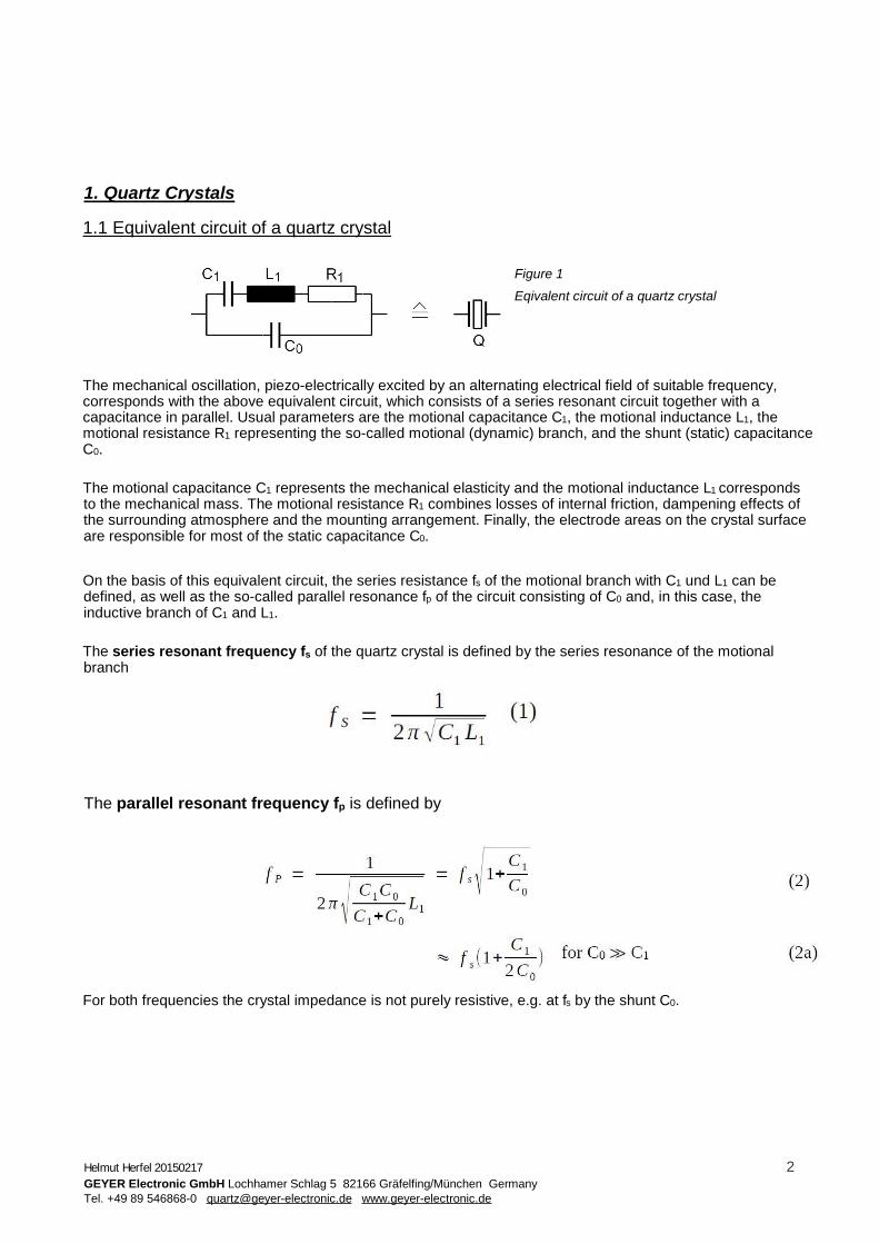
Figure 1
Eqivalent circuit of a quartz crystal
The mechanical oscillation, piezo-electrically excited by an alternating electrical field of suitable frequency, corresponds with the above equivalent circuit, which consists of a series resonant circuit together with a capacitance in parallel. Usual parameters are the motional capacitance C1, the motional inductance L1, the motional resistance R1 representing the so-called motional (dynamic) branch, and the shunt (static) capacitance C0. The motional capacitance C1 represents the mechanical elasticity and the motional inductance L1 corresponds to the mechanical mass. The motional resistance R1 combines losses of internal friction, dampening effects of the surrounding atmosphere and the mounting arrangement. Finally, the electrode areas on the crystal surface are responsible for most of the static capacitance C0. On the basis of this equivalent circuit, the series resistance fs of the motional branch with C1 und L1 can be defined, as well as the so-called parallel resonance fp of the circuit consisting of C0 and, in this case, the inductive branch of C1 and L1. The series resonant frequency fs of the quartz crystal is defined by the series resonance of the motional branch
The parallel resonant frequency fp is defined by
For both frequencies the crystal impedance is not purely resistive, e.g. at fs by the shunt C0.

Helmut Herfel 20150217 3 GEYER Electronic GmbH Lochhamer Schlag 5 82166 Gräfelfing/München Germany Tel. +49 89 546868-0 [email protected] www.geyer-electronic.de
Figures 2 and 3 show the impedance and the admittance corresponding to the equivalent circuit in figure 1. fs and fp are marked with little dots on the curves (fp according to equation 2, not 2a!). However, these curves correspond to component values, which cannot be realised with normal quartz crystals - but they can illustrate in principle the basic location and sequence of the characteristic frequency points. With normal quartz crystals the high quality factor prevents important points of the diagram to be shown completely without unrealistic deformation of scaling and curves. Figure 4 shows the admittance of a normal quartz crystal. The curve is nearly symmetric in respect to the real axis; the series resonance is very near to the point 1/R1. Using the impedance diagram (Figure 5), fs and other important points would lie unidentifiably close to zero and the far right parallel resonance is included to scale. Therefore, only the important low impedance values are depicted. The frequency where the impedance is real and of low resistance, is called resonant frequency fr (without the adjunct 'series'!). This important and easily measurable crystal parameter is, at least at not too-high crystal frequencies, only minimally higher than fs, which plays a minor role e.g. when ordering a crystal. This is equally valid with regard to the parallel resonant frequency fp: a reactive component exists at the parallel resonant frequency fp. The frequency where the crystal impedance is real (and of high resistance) is the anti-resonant frequency fa which is somewhat lower than fp. In Figures 2 and 3 the Nyquist diagrams of admittance and impedance shown which are valid for the above introduced equivalent circuit. These diagrams are calculated with component values that are not realizable with 'normal' quartz resonators. But they are meant, as has already mentioned, to show the basic location and sequence of important points.
Figure 2 und 3 Admittance (left) and impedance (right) of the equivalent circuit of Figure 1
The next two graphs show the results for a 'normal' quartz resonator. The loops in Figures 2 and 3 have (almost) become circles.
Helmut Herfel 20150217 4 GEYER Electronic GmbH Lochhamer Schlag 5 82166 Gräfelfing/München Germany Tel. +49 89 546868-0 [email protected] www.geyer-electronic.de
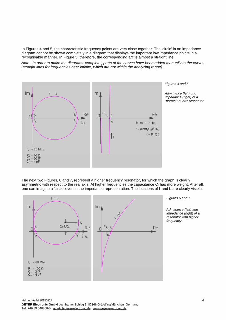
In Figures 4 and 5, the characteristic frequency points are very close together. The 'circle' in an impedance diagram cannot be shown completely in a diagram that displays the important low impedance points in a recognisable manner. In Figure 5, therefore, the corresponding arc is almost a straight line. Note: In order to make the diagrams 'complete', parts of the curves have been added manually to the curves (straight lines for frequencies near infinite, which are not within the analyzing range).
Figures 4 and 5
Admittance (left) und impedance (right) of a "normal" quartz resonator
The next two Figures, 6 and 7, represent a higher frequency resonator, for which the graph is clearly asymmetric with respect to the real axis. At higher frequencies the capacitance C0 has more weight. After all, one can imagine a 'circle' even in the impedance representation. The locations of fr and fs are clearly visible.
Figures 6 and 7
Admittance (left) and impedance (right) of a resonator with higher frequency
Helmut Herfel 20150217 5 GEYER Electronic GmbH Lochhamer Schlag 5 82166 Gräfelfing/München Germany Tel. +49 89 546868-0 [email protected] www.geyer-electronic.de
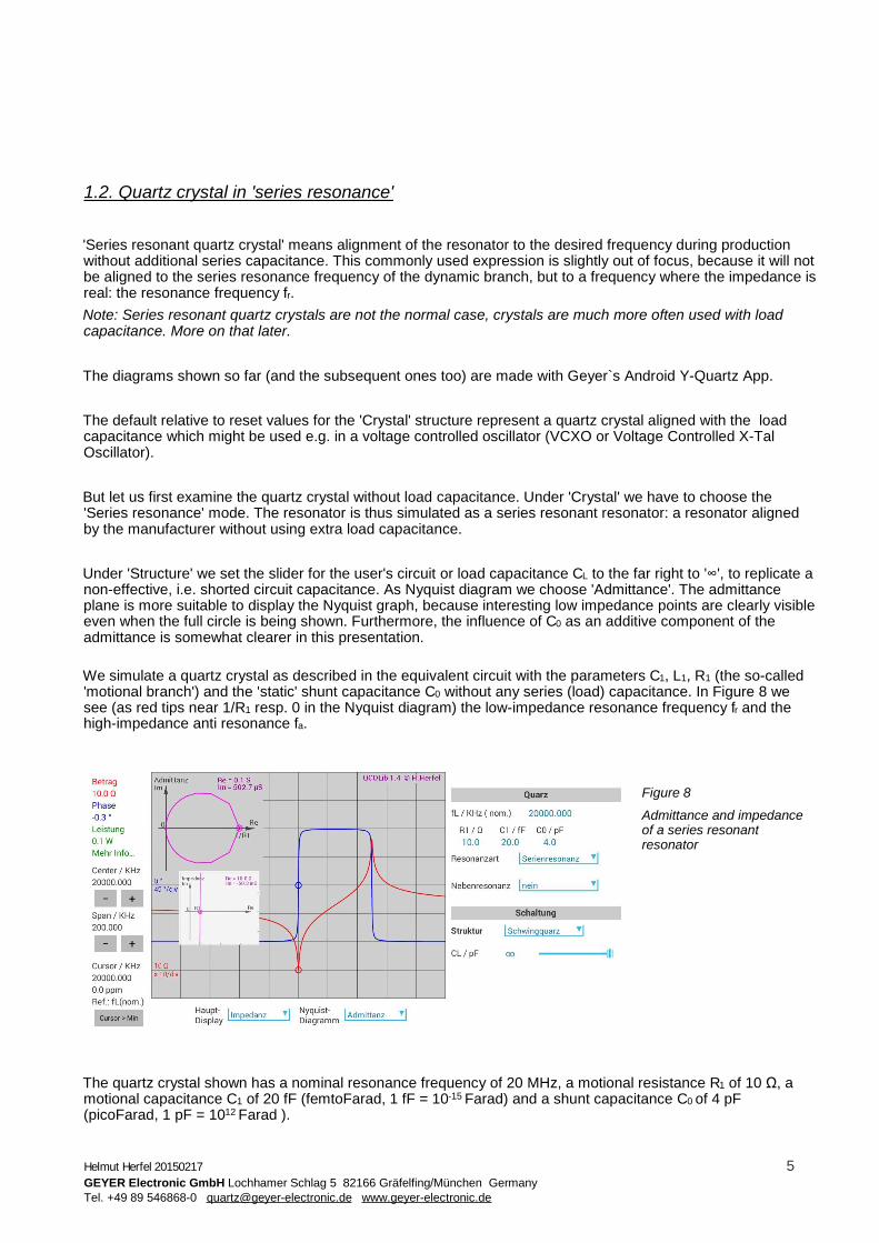
1.2. Quartz crystal in 'series resonance' 'Series resonant quartz crystal' means alignment of the resonator to the desired frequency during production without additional series capacitance. This commonly used expression is slightly out of focus, because it will not be aligned to the series resonance frequency of the dynamic branch, but to a frequency where the impedance is real: the resonance frequency fr. Note: Series resonant quartz crystals are not the normal case, crystals are much more often used with load capacitance. More on that later. The diagrams shown so far (and the subsequent ones too) are made with Geyer`s Android Y-Quartz App. The default relative to reset values for the 'Crystal' structure represent a quartz crystal aligned with the load capacitance which might be used e.g. in a voltage controlled oscillator (VCXO or Voltage Controlled X-Tal Oscillator). But let us first examine the quartz crystal without load capacitance. Under 'Crystal' we have to choose the 'Series resonance' mode. The resonator is thus simulated as a series resonant resonator: a resonator aligned by the manufacturer without using extra load capacitance. Under 'Structure' we set the slider for the user's circuit or load capacitance CL to the far right to '∞', to replicate a non-effective, i.e. shorted circuit capacitance. As Nyquist diagram we choose 'Admittance'. The admittance plane is more suitable to display the Nyquist graph, because interesting low impedance points are clearly visible even when the full circle is being shown. Furthermore, the influence of C0 as an additive component of the admittance is somewhat clearer in this presentation. We simulate a quartz crystal as described in the equivalent circuit with the parameters C1, L1, R1 (the so-called 'motional branch') and the 'static' shunt capacitance C0 without any series (load) capacitance. In Figure 8 we see (as red tips near 1/R1 resp. 0 in the Nyquist diagram) the low-impedance resonance frequency fr and the high-impedance anti resonance fa.
Figure 8
Admittance and impedance of a series resonant resonator
The quartz crystal shown has a nominal resonance frequency of 20 MHz, a motional resistance R1 of 10 Ω, a motional capacitance C1 of 20 fF (femtoFarad, 1 fF = 10-15 Farad) and a shunt capacitance C0 of 4 pF (picoFarad, 1 pF = 1012 Farad ).

Helmut Herfel 20150217 6 GEYER Electronic GmbH Lochhamer Schlag 5 82166 Gräfelfing/München Germany Tel. +49 89 546868-0 [email protected] www.geyer-electronic.de
The main display shows magnitude and phase response over frequency. The two resonances fr and fa are identified by the the zero crossings of the phase near to the two resonance peaks. In addition to the Nyquist admittance, the diagram shows the Nyquist impedance graph, at least the low impedance part of the too-big circle. The 'circles' for this not-very-high frequency resonator (20 MHz) are, in both representations almost symmetrical to the real axis. The arc below the real axis of the Nyquist admittance diagram corresponds to the section between the two extreme values of the red magnitude curve of the main impedance diagram. There, the quartz crystal is 'inductive', the phase of the admittance is negative (positive for the impedance), and the quartz crystal behavior outside of this range is 'capactive'.
1.2.1. Shunt capacitance, high frequencies
If we increase the simulated value of the shunt capacitance C0 to a (not very realistic) value of 40pF, the Nyquist graph become to lie somewhat higher. In addition, the high-impedance resonance fa moves closer to the low-impedance frequency fr. This effect corresponds to the now smaller term C1 / 2C0 in equation 2.
Figure 9 Series resonant resonator with extremely large C0
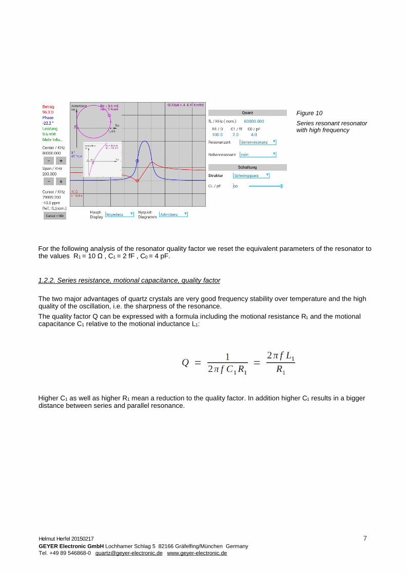
At very high frequencies, resonators to the 'circle' often lie much higher; in certain circumstances so high that they no longer intersect the real axis. An inductive C0-compensation can provide a remedy in such cases, both in production during alignment as well as in the application circuit. Figure 10 also shows as well marked frequency values the sequence of maximum impedance frequency (cursor), the series resonant frequency fs (right small purple dot) and resonance frequency fr (right intersection with the real axis).
Helmut Herfel 20150217 7 GEYER Electronic GmbH Lochhamer Schlag 5 82166 Gräfelfing/München Germany Tel. +49 89 546868-0 [email protected] www.geyer-electronic.de
Figure 10 Series resonant resonator with high frequency
For the following analysis of the resonator quality factor we reset the equivalent parameters of the resonator to the values R1 = 10 Ω , C1 = 2 fF , C0 = 4 pF.
1.2.2. Series resistance, motional capacitance, quality factor The two major advantages of quartz crystals are very good frequency stability over temperature and the high quality of the oscillation, i.e. the sharpness of the resonance. The quality factor Q can be expressed with a formula including the motional resistance R1 and the motional capacitance C1 relative to the motional inductance L1:
Higher C1 as well as higher R1 mean a reduction to the quality factor. In addition higher C1 results in a bigger distance between series and parallel resonance.
Helmut Herfel 20150217 8 GEYER Electronic GmbH Lochhamer Schlag 5 82166 Gräfelfing/München Germany Tel. +49 89 546868-0 [email protected] www.geyer-electronic.de
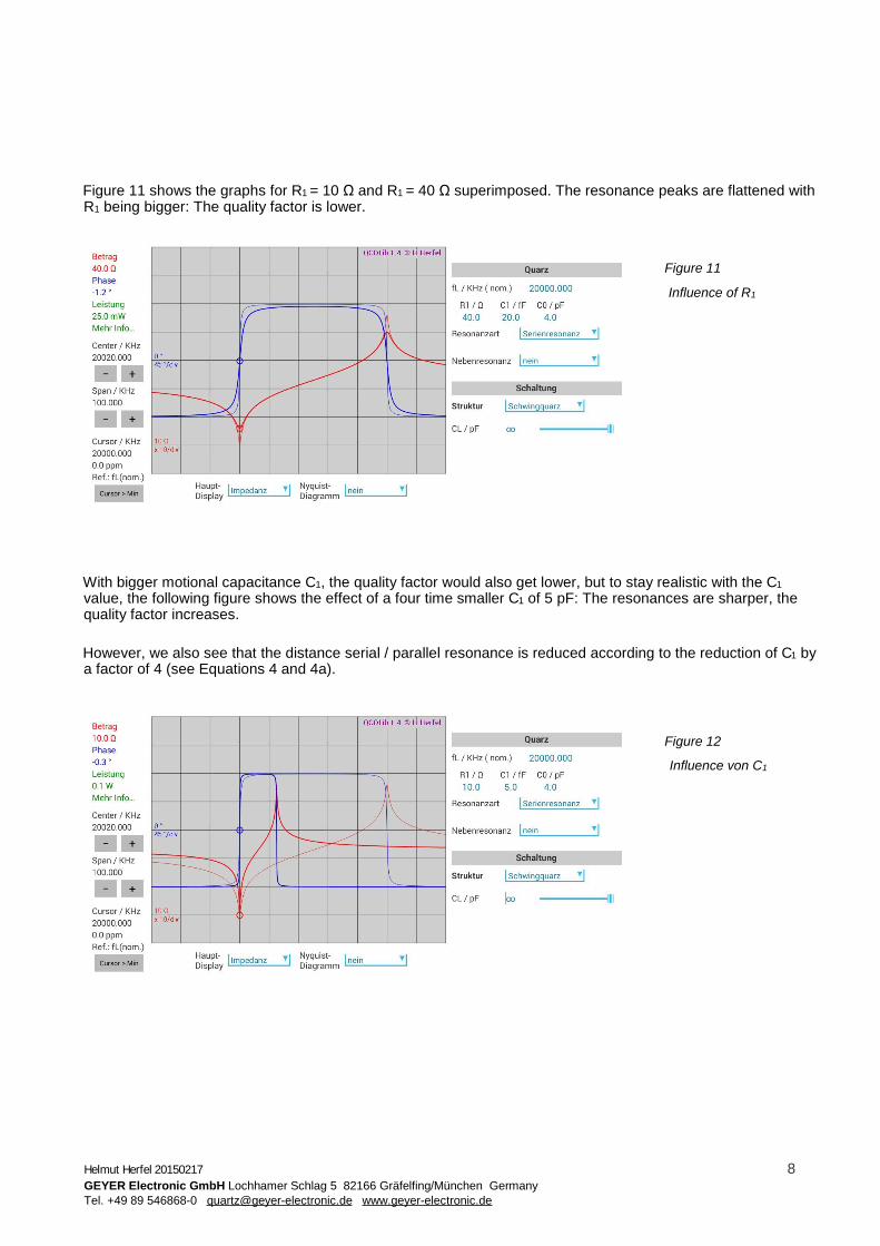
Figure 11 shows the graphs for R1 = 10 Ω and R1 = 40 Ω superimposed. The resonance peaks are flattened with R1 being bigger: The quality factor is lower.
Figure 11
Influence of R1
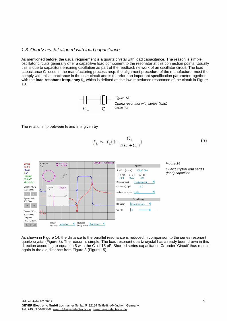
With bigger motional capacitance C1, the quality factor would also get lower, but to stay realistic with the C1 value, the following figure shows the effect of a four time smaller C1 of 5 pF: The resonances are sharper, the quality factor increases. However, we also see that the distance serial / parallel resonance is reduced according to the reduction of C1 by a factor of 4 (see Equations 4 and 4a).
Figure 12
Influence von C1
Helmut Herfel 20150217 9 GEYER Electronic GmbH Lochhamer Schlag 5 82166 Gräfelfing/München Germany Tel. +49 89 546868-0 [email protected] www.geyer-electronic.de
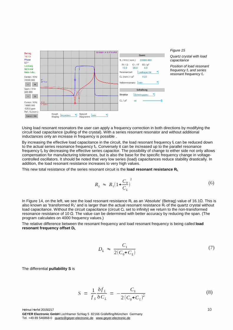
1.3. Quartz crystal aligned with load capacitance As mentioned before, the usual requirement is a quartz crystal with load capacitance. The reason is simple: oscillator circuits generally offer a capacitive load component to the resonator at this connection points. Usually this is due to capacitors ensuring oscillation as part of the feedback network of an oscillator circuit. The load capacitance CL used in the manufacturing process resp. the alignment procedure of the manufacturer must then comply with this capacitance in the user circuit and is therefore an important specification parameter together with the load resonant frequency fL, which is defined as the low impedance resonance of the circuit in Figure 13.
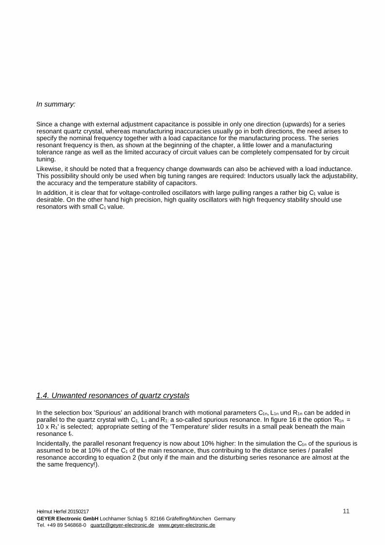
Figure 13
Quartz resonator with series (load) capacitor
The relationship between fS and fL is given by
Figure 14
Quartz crystal with series (load) capacitor
As shown in Figure 14, the distance to the parallel resonance is reduced in comparison to the series resonant quartz crystal (Figure 8). The reason is simple: The load resonant quartz crystal has already been drawn in this direction according to equation 5 with the CL of 15 pF. Shorted series capacitance CL under 'Circuit' thus results again in the old distance from Figure 8 (Figure 15).
Helmut Herfel 20150217 10 GEYER Electronic GmbH Lochhamer Schlag 5 82166 Gräfelfing/München Germany Tel. +49 89 546868-0 [email protected] www.geyer-electronic.de
Figure 15
Quartz crystal with load capacitance
Position of load resonant frequency fL and series resonant frequency fs
Using load resonant resonators the user can apply a frequency correction in both directions by modifying the circuit load capacitance (pulling of the crystal). With a series resonant resonator and without additional inductances only an increase in frequency is possible . By increasing the effective load capacitance in the circuit, the load resonant frequency fL can be reduced down to the actual series resonance frequency fs. Conversely it can be increased up to the parallel resonance frequency fp by decreasing the effective series capacitor. The possibility of change to either side not only allows compensation for manufacturing tolerances, but is also the base for the specific frequency change in voltage-controlled oscillators. It should be noted that very low series (load) capacitances reduce stability drastically. In addition, the load resonant resistance increases to very high values. This new total resistance of the series resonant circuit is the load resonant resistance RL
In Figure 14, on the left, we see the load resonant resistance RL as an 'Absolute' (Betrag) value of 16.1Ω. This is also known as 'transformed R1' and is larger than the actual resonant resistance Rr of the quartz crystal without load capacitance. Without the circuit capacitance (circuit CL set to infinity) we return to the non-transformed resonance resistance of 10 Ω. The value can be determined with better accuracy by reducing the span. (The program calculates on 4000 frequency values.) The relative difference between the resonant frequency and load resonant frequency is being called load resonant frequency offset DL
The differential pullability S is
Helmut Herfel 20150217 11 GEYER Electronic GmbH Lochhamer Schlag 5 82166 Gräfelfing/München Germany Tel. +49 89 546868-0 [email protected] www.geyer-electronic.de
In summary: Since a change with external adjustment capacitance is possible in only one direction (upwards) for a series resonant quartz crystal, whereas manufacturing inaccuracies usually go in both directions, the need arises to specify the nominal frequency together with a load capacitance for the manufacturing process. The series resonant frequency is then, as shown at the beginning of the chapter, a little lower and a manufacturing tolerance range as well as the limited accuracy of circuit values can be completely compensated for by circuit tuning. Likewise, it should be noted that a frequency change downwards can also be achieved with a load inductance. This possibility should only be used when big tuning ranges are required: Inductors usually lack the adjustability, the accuracy and the temperature stability of capacitors. In addition, it is clear that for voltage-controlled oscillators with large pulling ranges a rather big C1 value is desirable. On the other hand high precision, high quality oscillators with high frequency stability should use resonators with small C1 value.
1.4. Unwanted resonances of quartz crystals
In the selection box 'Spurious' an additional branch with motional parameters C1n, L1n und R1n can be added in parallel to the quartz crystal with C1, L1 and R1: a so-called spurious resonance. In figure 16 it the option 'R1n = 10 x R1' is selected; appropriate setting of the 'Temperature' slider results in a small peak beneath the main resonance fr. Incidentally, the parallel resonant frequency is now about 10% higher: In the simulation the C1n of the spurious is assumed to be at 10% of the C1 of the main resonance, thus contribuing to the distance series / parallel resonance according to equation 2 (but only if the main and the disturbing series resonance are almost at the the same frequency!).
Helmut Herfel 20150217 12 GEYER Electronic GmbH Lochhamer Schlag 5 82166 Gräfelfing/München Germany Tel. +49 89 546868-0 [email protected] www.geyer-electronic.de
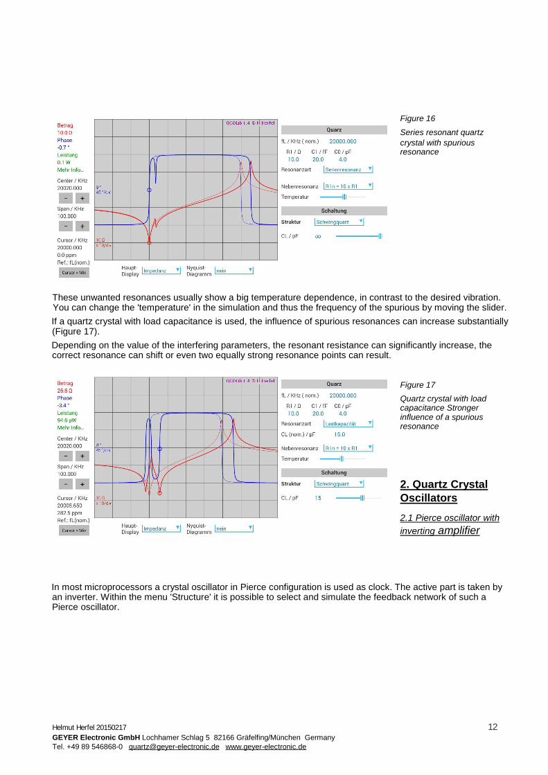
Figure 16
Series resonant quartz crystal with spurious resonance
These unwanted resonances usually show a big temperature dependence, in contrast to the desired vibration. You can change the 'temperature' in the simulation and thus the frequency of the spurious by moving the slider. If a quartz crystal with load capacitance is used, the influence of spurious resonances can increase substantially (Figure 17). Depending on the value of the interfering parameters, the resonant resistance can significantly increase, the correct resonance can shift or even two equally strong resonance points can result.
Figure 17 Quartz crystal with load capacitance Stronger influence of a spurious resonance
2. Quartz Crystal Oscillators
2.1 Pierce oscillator with inverting amplifier
In most microprocessors a crystal oscillator in Pierce configuration is used as clock. The active part is taken by an inverter. Within the menu 'Structure' it is possible to select and simulate the feedback network of such a Pierce oscillator.
Helmut Herfel 20150217 13 GEYER Electronic GmbH Lochhamer Schlag 5 82166 Gräfelfing/München Germany Tel. +49 89 546868-0 [email protected] www.geyer-electronic.de
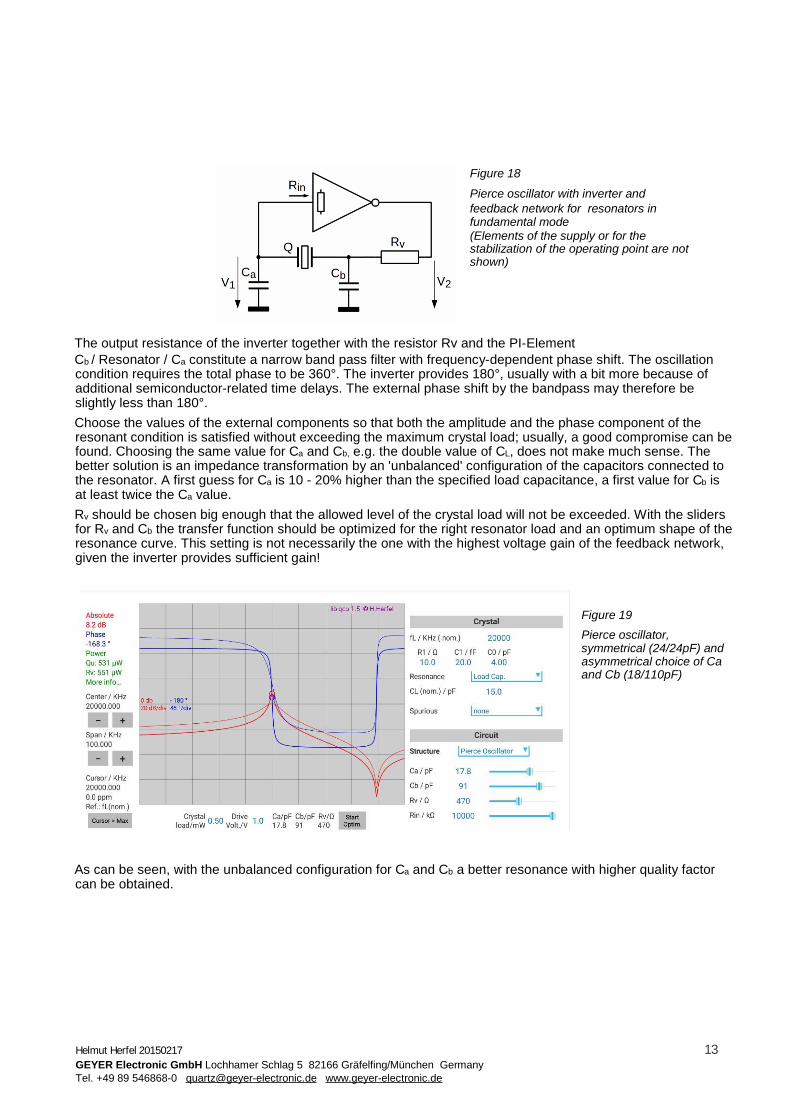
Figure 18
Pierce oscillator with inverter and feedback network for resonators in fundamental mode (Elements of the supply or for the stabilization of the operating point are not shown)
The output resistance of the inverter together with the resistor Rv and the PI-Element Cb / Resonator / Ca constitute a narrow band pass filter with frequency-dependent phase shift. The oscillation condition requires the total phase to be 360°. The inverter provides 180°, usually with a bit more because of additional semiconductor-related time delays. The external phase shift by the bandpass may therefore be slightly less than 180°. Choose the values of the external components so that both the amplitude and the phase component of the resonant condition is satisfied without exceeding the maximum crystal load; usually, a good compromise can be found. Choosing the same value for Ca and Cb, e.g. the double value of CL, does not make much sense. The better solution is an impedance transformation by an 'unbalanced' configuration of the capacitors connected to the resonator. A first guess for Ca is 10 - 20% higher than the specified load capacitance, a first value for Cb is at least twice the Ca value. Rv should be chosen big enough that the allowed level of the crystal load will not be exceeded. With the sliders for Rv and Cb the transfer function should be optimized for the right resonator load and an optimum shape of the resonance curve. This setting is not necessarily the one with the highest voltage gain of the feedback network, given the inverter provides sufficient gain!
Figure 19 Pierce oscillator, symmetrical (24/24pF) and asymmetrical choice of Ca and Cb (18/110pF)
As can be seen, with the unbalanced configuration for Ca and Cb a better resonance with higher quality factor can be obtained.
Helmut Herfel 20150217 14 GEYER Electronic GmbH Lochhamer Schlag 5 82166 Gräfelfing/München Germany Tel. +49 89 546868-0 [email protected] www.geyer-electronic.de
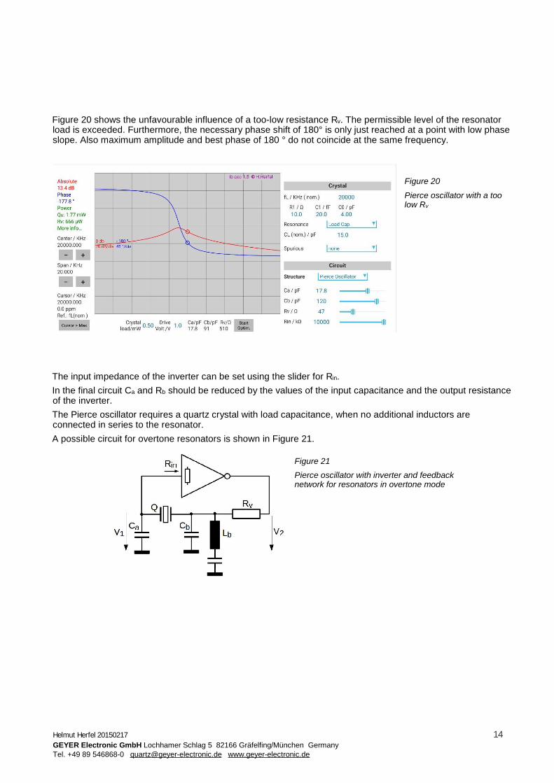
Figure 20 shows the unfavourable influence of a too-low resistance Rv. The permissible level of the resonator load is exceeded. Furthermore, the necessary phase shift of 180° is only just reached at a point with low phase slope. Also maximum amplitude and best phase of 180 ° do not coincide at the same frequency.
Figure 20
Pierce oscillator with a too low Rv
The input impedance of the inverter can be set using the slider for Rin. In the final circuit Ca and Rb should be reduced by the values of the input capacitance and the output resistance of the inverter. The Pierce oscillator requires a quartz crystal with load capacitance, when no additional inductors are connected in series to the resonator. A possible circuit for overtone resonators is shown in Figure 21.
Figure 21
Pierce oscillator with inverter and feedback network for resonators in overtone mode
Helmut Herfel 20150217 15 GEYER Electronic GmbH Lochhamer Schlag 5 82166 Gräfelfing/München Germany Tel. +49 89 546868-0 [email protected] www.geyer-electronic.de
2.2 Colpitts oscillator with non-inverting amplifier For the Colpitts oscillator a non-inverting element supplies the necessary gain. The menu 'Structure' offers the possibility to simulate the feedback network of this oscillator type.
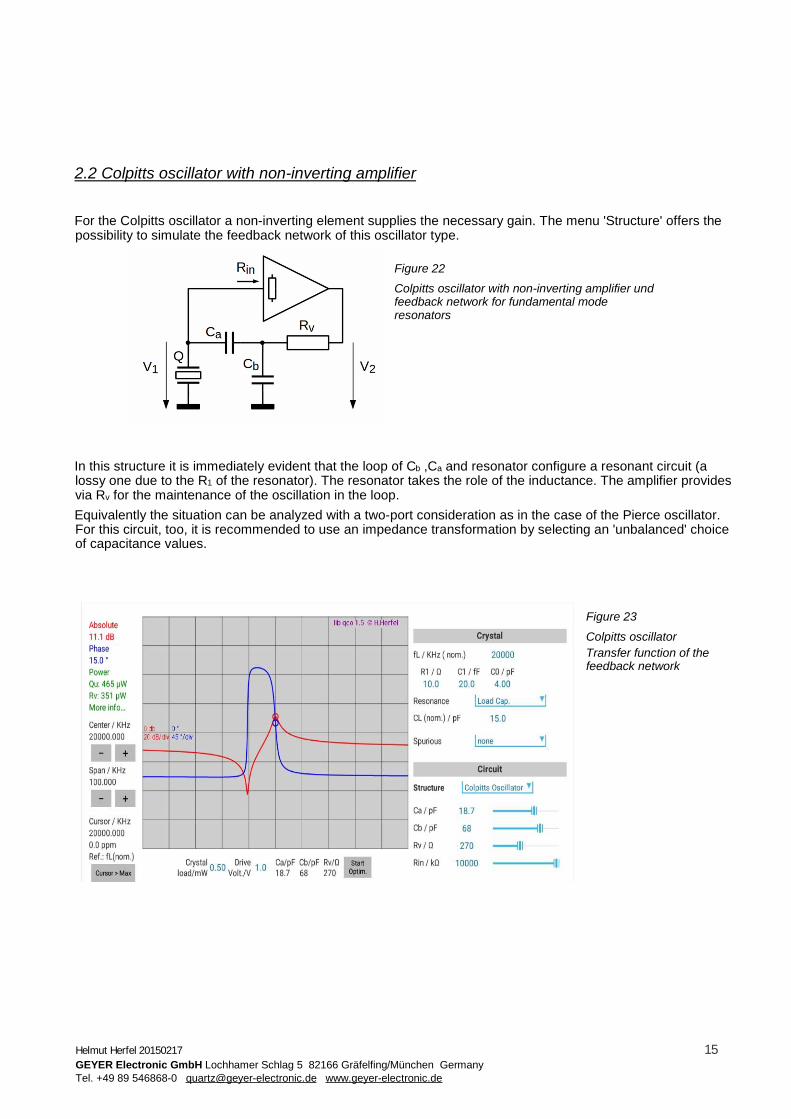
Figure 22
Colpitts oscillator with non-inverting amplifier und feedback network for fundamental mode resonators
In this structure it is immediately evident that the loop of Cb ,Ca and resonator configure a resonant circuit (a lossy one due to the R1 of the resonator). The resonator takes the role of the inductance. The amplifier provides via Rv for the maintenance of the oscillation in the loop. Equivalently the situation can be analyzed with a two-port consideration as in the case of the Pierce oscillator. For this circuit, too, it is recommended to use an impedance transformation by selecting an 'unbalanced' choice of capacitance values.
Figure 23
Colpitts oscillator Transfer function of the feedback network