sherief reda division of engineering, brown...
TRANSCRIPT

Physical Design of Digital Integrated Circuits(EN0291 S40)
Sherief RedaDivision of Engineering, Brown University
Fall 2006
• Course objective• Brief tour of IC physical design • Projects overview• Survey of papers and industry products
Lecture 01: the big picture
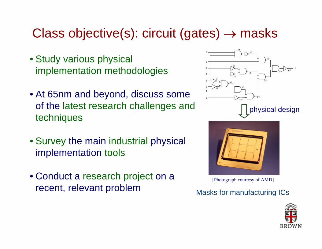
Class objective(s): circuit (gates) → masks
[Photograph courtesy of AMD]
• Study various physical implementation methodologies
• At 65nm and beyond, discuss some of the latest research challenges and techniques
• Survey the main industrial physical implementation tools
• Conduct a research project on a recent, relevant problem
physical design
Masks for manufacturing ICs

What do designers really care about?
• Design Objectives:– Power (dynamic/static)– Timing (frequency)– Area (cost/yield)– Yield (cost)
• Challenges:– Manufacturing technology– Leakage power– Interconnect delay– Variability– Reliability

Circuit entities eventually are either transistors or interconnects
How do you manufacture them?
NMOS transistor Metal interconnects

How do ICs get manufactured?
[Advanced Micro Devices from Quirck/Serda]
Oxidation(Field oxide)
Silicon substrate
Silicon dioxideSilicon dioxide
oxygen
PhotoresistDevelop
oxideoxide
PhotoresistCoating
photoresistphotoresist
Mask-WaferAlignment and Exposure
Mask
UV light
Exposed Photoresist
exposedphotoresistexposed
photoresist
GGS D
Active Regions
top nitridetop nitride
S DGG
silicon nitridesilicon nitride
NitrideDeposition
Contact holes
S DGG
ContactEtch
Ion Implantation
resis
tre
sist
resis
t
oxox DG
Scanning ion beam
S
Metal Deposition and
Etch
drainS DGG
Metal contacts
PolysiliconDeposition
polysiliconpolysilicon
Silane gas
Dopant gas
Oxidation(Gate oxide)
gate oxidegate oxide
oxygen
PhotoresistStrip
oxideoxide
RF Power
RF Power
Ionized oxygen gas
OxideEtch
photoresistphotoresistoxideoxide
RF Power
RF Power
Ionized CF4 gas
PolysiliconMask and Etch
RF Power
RF Power
oxideoxideoxide
Ionized CCl4 gas
poly
gate
poly
gate
RF Power
RF Power
[Check out this too http://www.appliedmaterials.com/HTMAC/animated.html]

And the end result is:
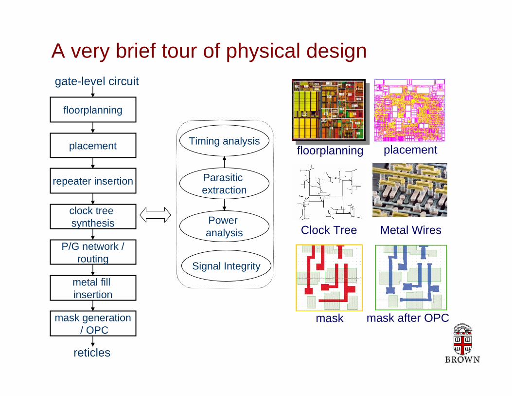
A very brief tour of physical design
placementfloorplanning
floorplanning
placement
repeater insertion
clock tree synthesis
P/G network /routing
metal fill insertion
mask generation/ OPC
gate-level circuit
reticles
Timing analysis
Parasitic extraction
Power analysis
Signal Integrity
mask mask after OPC
Metal Wires Clock Tree

Class breakup
Topic i main ideas and techniques
(sreda)
Topic i-1 papers / industrial tool survey(class participation)
5-10 minute break
Topic i+1 main ideas and techniques
(sreda)
Topic i papers / industrial tool survey(class participation)
5-10 minute break
• Class participation (30% of final grade)• Class project (70% of final grade)
• Course objective • Brief tour of IC physical design • Projects overview• Survey of papers and industry products
Lecture 01: the big picture
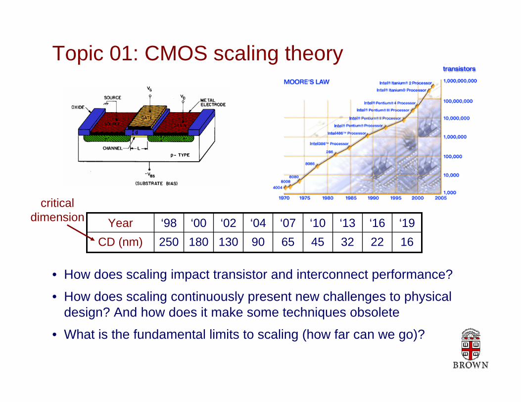
Topic 01: CMOS scaling theory
• How does scaling impact transistor and interconnect performance?
• How does scaling continuously present new challenges to physicaldesign? And how does it make some techniques obsolete
• What is the fundamental limits to scaling (how far can we go)?
22‘16
45‘10
16‘19
32‘13
90‘04
65‘07
130180250CD (nm)‘02‘00‘98Year
criticaldimension

Topic 01: CMOS scaling theory
gate delaylocal (scaled)
wiresglobal(repeaters)
global(no repeaters)
[Moore, ISSCC’03][ITRS’03]active
leakage

Topic 02: Process variability• At 180nm and beyond, random sources of variation affect IC
performance
temperaturedopant fluctuationsruntimeprocess
random sources
gate length/width variationsIR dropgate oxide thickness
→ Performance/power is no longer deterministic, but rather a random variable with an associated probability distribution
0.91.01.11.21.31.4
0 5 10 15 20Normalized Leakage [source: Intel @ 180nm]
Normalized Frequency
20x
30%

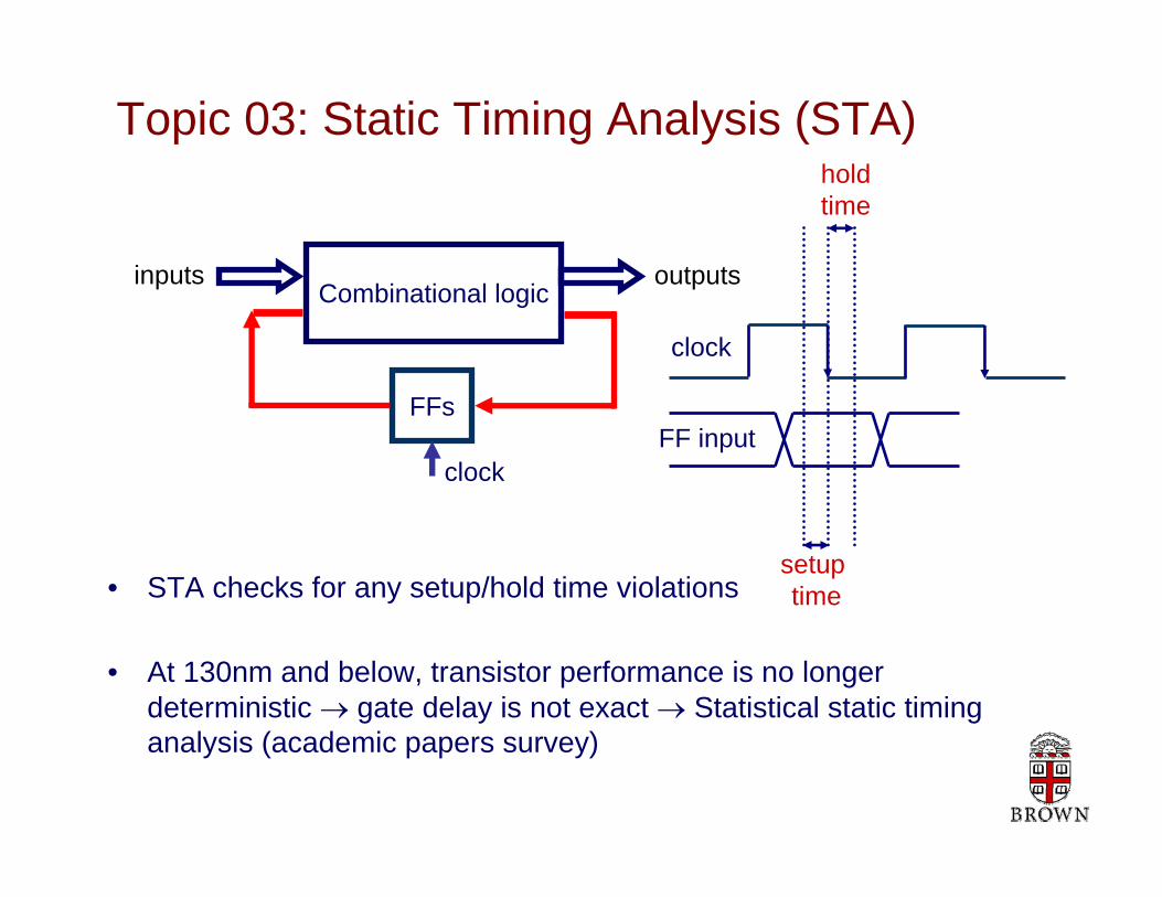
Topic 03: Static timing analysis (STA)
I1I2I3I4
I5I6
O1
O2
• What is the worst delay of this circuit? → determines the frequency of operation
• What are the critical path(s) that lead to this delay? → perhaps timing can be improved if we adjust them
C17 from ISCAS’85 benchmarks
Topic 03: Static Timing Analysis (STA)
• STA checks for any setup/hold time violations
• At 130nm and below, transistor performance is no longer deterministic → gate delay is not exact → Statistical static timing analysis (academic papers survey)
Combinational logicinputs outputs
FFs
clock
clock
setup time
holdtime
FF input

Topic 04: Power analysis and optimization
• Total Power = static + dynamic + short
factors capacitance
switching frequencyvoltageLeakage factors
transistor width/length,
threshold Voltagetemperature
factorsvoltage
trans. timeswitching freq
NMOS transistor
A Z
Vdd
CMOS inverter
Optimizationstweak these
factors to minimize power with little impact on performance
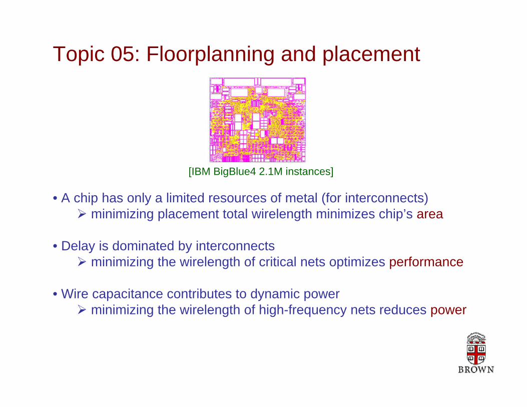
Topic 05: Floorplanning and placement
• A chip has only a limited resources of metal (for interconnects)minimizing placement total wirelength minimizes chip’s area
• Delay is dominated by interconnectsminimizing the wirelength of critical nets optimizes performance
• Wire capacitance contributes to dynamic powerminimizing the wirelength of high-frequency nets reduces power
[IBM BigBlue4 2.1M instances]
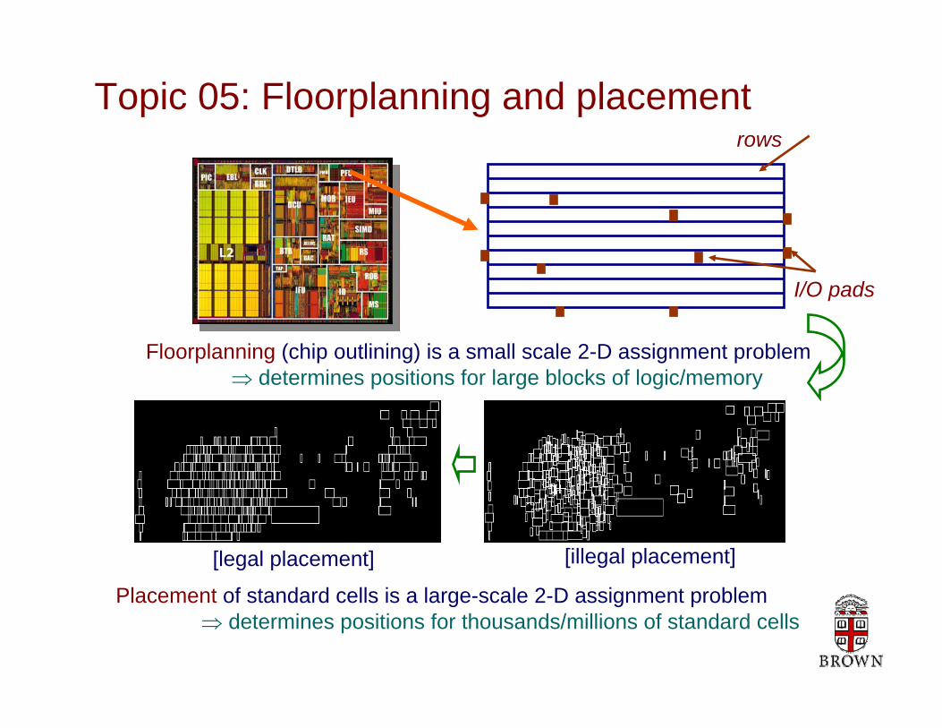
Topic 05: Floorplanning and placement
Floorplanning (chip outlining) is a small scale 2-D assignment problem ⇒ determines positions for large blocks of logic/memory
rows
I/O pads
Placement of standard cells is a large-scale 2-D assignment problem ⇒ determines positions for thousands/millions of standard cells
[illegal placement][legal placement]
minimize demand on metal resources and
reduces power
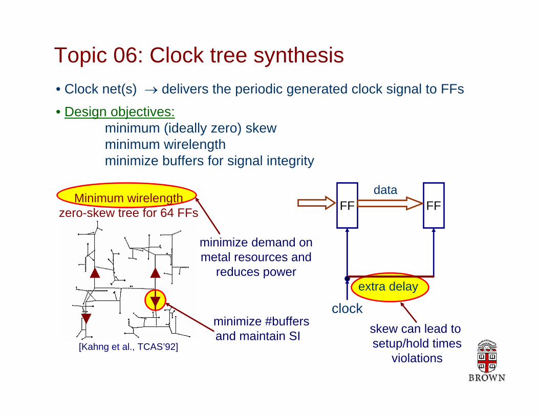
skew can lead to setup/hold times
violations
Topic 06: Clock tree synthesis• Clock net(s) → delivers the periodic generated clock signal to FFs
• Design objectives:minimum (ideally zero) skewminimum wirelengthminimize buffers for signal integrity
FF FFdata
clockextra delay
[Kahng et al., TCAS’92]
Minimum wirelength zero-skew tree for 64 FFs
minimize #buffersand maintain SI
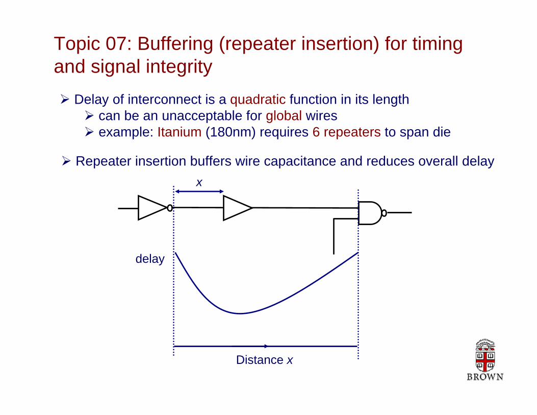
Topic 07: Buffering (repeater insertion) for timing and signal integrity
Delay of interconnect is a quadratic function in its lengthcan be an unacceptable for global wiresexample: Itanium (180nm) requires 6 repeaters to span die
Repeater insertion buffers wire capacitance and reduces overall delay
delay
Distance x
x

Topic 07: Buffering (repeater insertion) for timing and signal integrity
sourcesink
sinkWhat is the minimum number of repeaters to meet timing on this net?
The situation is complicated in case of multi-pin nets:
Repeater estimation for Itanium
Repeater Stations

Topic 08: Design and analysis of power supply networks
[Blaauw et al., DAC98]
PowerPC 750 power grid
PowerPC 750 IR-drop map
• Power supply network delivers Vdd/Gnd signals to all components.
Main challenges:
1. IR drop: voltage at delivery point is degraded than the ideal voltage
• performance drop• signal integrity problems
2. electromigration
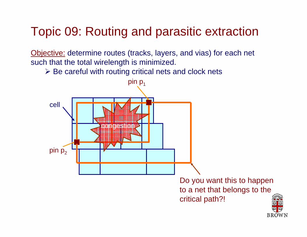
Topic 09: Routing and parasitic extraction
pin p1
pin p2
Do you want this to happen to a net that belongs to the critical path?!
Objective: determine routes (tracks, layers, and vias) for each net such that the total wirelength is minimized.
Be careful with routing critical nets and clock nets
cell
congestion

Topic 09: Routing and parasitic extraction
source
sink
sink
map to layers
create vias
Multi-pin nets add more complexity in routing
After all routes are determined, you can calculate the parasitic capacitance between each wire and its neighbors
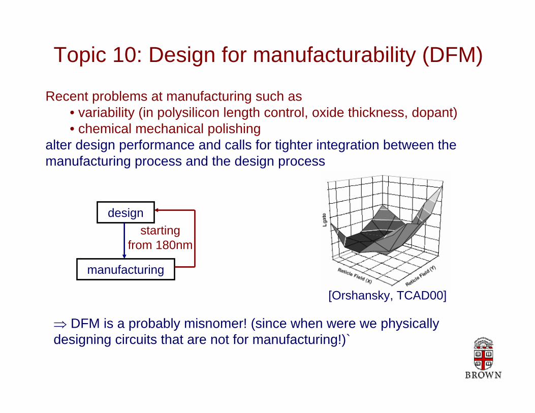
Topic 10: Design for manufacturability (DFM)
⇒ DFM is a probably misnomer! (since when were we physically designing circuits that are not for manufacturing!)`
Recent problems at manufacturing such as• variability (in polysilicon length control, oxide thickness, dopant)• chemical mechanical polishing
alter design performance and calls for tighter integration between the manufacturing process and the design process
design
manufacturing
startingfrom 180nm
[Orshansky, TCAD00]
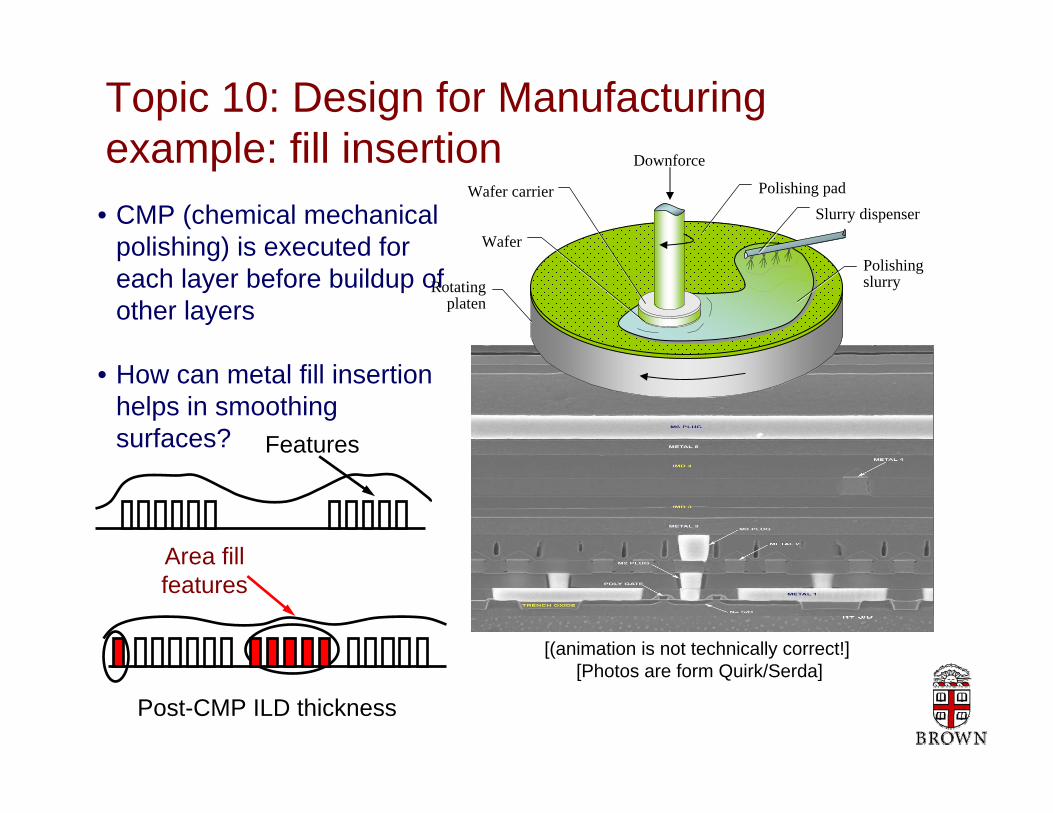
Topic 10: Design for Manufacturing example: fill insertion
Wafer
Wafer carrier
Rotating platen
Polishing slurry
Slurry dispenserPolishing pad
Downforce
• CMP (chemical mechanical polishing) is executed for each layer before buildup of other layers
• How can metal fill insertion helps in smoothing surfaces?
[(animation is not technically correct!][Photos are form Quirk/Serda]
Features
Post-CMP ILD thickness
Area fillfeatures

Topic 11: mask preparation and resolution enhancement techniques (RET)
original layout
MEBES
[mask writer]
fractured layout
fractured layout into polygons(rectangles and trapezoids)
Did we just forget something?!
GDSII
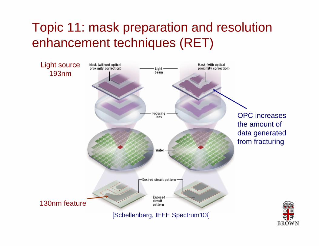
Topic 11: mask preparation and resolution enhancement techniques (RET)
Light source 193nm
130nm feature[Schellenberg, IEEE Spectrum’03]
OPC increases the amount of data generated from fracturing

Extra topics:
• FPGA physical design• IO assignment and packaging• Design rule checking
• Course objective • Brief tour of IC physical design • Projects overview• Survey of papers and industry products
Lecture 01: the big picture
Project slides omitted

• Course objective • Brief tour of IC physical design • Projects overview• Survey of papers and industry products
Lecture 01: the big picture

Guidelines for academic paper reviews
• Describe the problem the paper addresses – Why is the problem relevant (past/now/future)?– Has this problem been addressed before? – If yes, what is the new here?– If no, is it meaningful?– Assume you solve the problem, how will this change the world?
• Describe the methodology of the solution– Why is this a good solution?– Are they are any wrong/good assumptions/constraints?– Are there any approximations? How good are they?
• Describe the experimental framework– Benchmark / tools used (academic / industrial)– Are the results compelling and competitive?– Are the results possible to duplicate?– Did the results proof beyond doubt that this is a useful approach

Guidelines for industry Industrial tool survey• Describe the purpose of the tool and how it helps the IC
designer.• Describe the main inputs/outputs of the tool.• Possibly describe the methodology used by the tool
(search product sheets / websites / US patent office)• Describe the possible options taken by the tool• Describe the main strengths/weakness of the tool.• (Compare the competitiveness of the tool to other tools.)• Be simple and only explain what you understood
(product review can be frustrating)• Present the tool from a technology point of view, not a
software (or marketing) point of view (avoid marketing propaganda)
• Check the possibility of getting a trial version.

Sources for information on tools
• Company websites• US Patent office• Google• EEtimes• Deepchip.com• Edn.com

References
• EDA for Integrated Circuits Handbook (Volume 2), Scheffer/Lavagno/G. Martin, CRC Press.
• Algorithms for VLSI Physical Design Automation, Sherwani, 3rd Edition, KAP
• Design of High-Performance Microprocessor Circuits, Chandraksan/Bowhill/Fox, IEEE Press.
• CMOS VLSI Design, Weste/Harris, 3rd edition, Addison-Wesley.
• Semiconductor Manufacturing Technology, Quirk/Serda, Prentice Hall.
Key Websites
• http://www.google.com• http://www.eetimes.com• http://www.deepchip.com• http://www.uspto.gov/patft/index.html• http://www.synopsys.com• http://www.cadence.com• http://www.dac.com• http://www.itrs.net/