sgm7227 high speed usb 2.0 (480mbps) dpdt analog switch · high speed usb 2.0 sgm7227 (480mbps)...
TRANSCRIPT

SGM7227 High Speed USB 2.0 (480Mbps) DPDT Analog Switch
GENERAL DESCRIPTION The SGM7227 is a high-speed, low-power double-pole/ double-throw (DPDT) analog switch that operates from a single 1.8V to 4.3V power supply. SGM7227 is designed for the switching of high-speed USB 2.0 signals in handset and consumer applications, such as cell phones, digital cameras, and notebooks with hubs or controllers with limited USB I/Os. The SGM7227 has low bit-to-bit skew and high channel-to-channel noise isolation, and is compatible with various standards, such as high-speed USB 2.0 (480 Mbps). Each switch is bidirectional and offers little or no attenuation of the high-speed signals at the outputs. Its bandwidth is wide enough to pass high-speed USB 2.0 differential signals (480 Mb/s) with good signal integrity. The SGM7227 contains special circuitry on the D+/D- pins which allows the device to withstand a VBUS short to D+ or D- when the USB devices are either powered off or powered on. SGM7227 is available in Green UTQFN1.8×1.4-10L and MSOP10 packages. It operates over an ambient temperature range of -40 to +85. APPLICATIONS Route Signals for USB 2.0 MP3 and Other Personal Media Players Digital Cameras and Camcorders Portable Instrumentation Set-Top Box PDAs
FEATURES RON is Typically 5Ω at 3.0V Voltage Operation: 1.8V to 4.3V Fast Switching Times:
tON 15ns tOFF 20ns
Crosstalk: -30dB at 250MHz Off-Isolation: -35dB at 250MHz Rail-to-Rail Input and Output Operation Break-Before-Make Switching Extended Industrial Temperature Range:
-40 to +85
Available in Green UTQFN1.8×1.4-10L and MSOP10 Packages
BLOCK DIAGRAM
D+HSD2+
HSD1+
D-HSD2-
HSD1-
LOGIC
SOE
REV. ASG Micro Limited www.sg-micro.com

High Speed USB 2.0 SGM7227 (480Mbps) DPDT Analog Switch
2SG Micro Limited www.sg-micro.com
PACKAGE/ORDERING INFORMATION
MODEL PIN- PACKAGE
SPECIFIED TEMPERATURE
RANGE
ORDERING NUMBER
PACKAGE MARKING
PACKAGE OPTION
MSOP10 -40 to +85 SGM7227YMS10G/TR SGM7227YMS10 Tape and Reel, 3000SGM7227
UTQFN1.8×1.4-10L -40 to +85 SGM7227YUWQ10G/TR 7227 Tape and Reel, 3000
ABSOLUTE MAXIMUM RATINGS VCC to GND................................................................ 0V to 4.6V Analog, Digital voltage range .....................-0.3V to (VCC) + 0.3V Continuous Current HSDn or Dn……..............................±50mA Peak Current HSDn or Dn……......................................±100mA Operating Temperature Range............................-40 to +85
Junction Temperature....................................................... 150
Storage Temperature.........................................-65 to +150
Lead Temperature (soldering, 10s)...................................260 ESD Susceptibility HBM (UTQFN1.8×1.4-10L)…………………………………4000V MM (UTQFN1.8×1.4-10L) …………………………………...400V
NOTE: Stresses beyond those listed under “Absolute Maximum Ratings” may cause permanent damage to the device. These are stress ratings only, and functional operation of the device at these or any other conditions beyond those indicated in the operational sections of the specifications is not implied. Exposure to absolute maximum rating conditions for extended periods may affect device reliability.
CAUTION This integrated circuit can be damaged by ESD if you don’t pay attention to ESD protection. SGMICRO recommends that all integrated circuits be handled with appropriate precautions. Failure to observe proper handling and installation procedures can cause damage. ESD damage can range from subtle performance degradation to complete device failure. Precision integrated circuits may be more susceptible to damage because very small parametric changes could cause the device not to meet its published specifications.

High Speed USB 2.0 SGM7227 (480Mbps) DPDT Analog Switch
3SG Micro Limited www.sg-micro.com
PIN CONFIGURATIONS (TOP VIEW)
OE
HSD1-6
7
8
9
101
2
3
4
5
S
D-
HSD2-D+
GND
VCC
HSD1+
MSOP10
HSD2+
UTQFN1.8×1.4-10L
HSD2+
HSD1+
1 2
5
4
3
67
8
9
10
D+
GND
D-
HSD2-
HSD1-
OE
VCC
S
PIN DESCRIPTION
PIN UTQFN1.8×1.4-10L MSOP10
NAME FUNCTION
9 1 VCC Power Supply 3 5 GND Ground 10 2 S Select Input 8 10 OE Output Enable 5 7 HSD1+ Multiplexed Source Inputs 4 6 HSD1- Multiplexed Source Inputs 7 9 HSD2+ Multiplexed Source Inputs 6 8 HSD2- Multiplexed Source Inputs 1 3 D+ USB Data Bus 2 4 D- USB Data Bus
FUNCTION TABLE
OE S HSD1+, HSD1- HSD2+, HSD2-
0 0 ON OFF 0 1 OFF ON 1 × OFF OFF
Switches Shown For Logic “0” Input

High Speed USB 2.0 SGM7227 (480Mbps) DPDT Analog Switch
4SG Micro Limited www.sg-micro.com
ELECTRICAL CHARACTERISTICS (VCC = +3.3V, TA = +25, unless otherwise noted.)
PARAMETER SYMBOL CONDITIONS MIN TYP MAX UNITSANALOG SWITCH Analog I/O Voltage (HSD1+, HSD1-, HSD2+, HSD2-) VIS 0 VCC V
On-Resistance RON VCC = 3.0V, VIS = 0V to 0.4V, ID = 8mA, Test Circuit 1 5 9 Ω
On-Resistance Match Between Channels ∆RON VCC = 3.0V, VIS = 0V to 0.4V,
ID = 8mA, Test Circuit 1 0.3 0.8 Ω
On-Resistance Flatness RFLAT(ON) VCC = 3.0V, VIS = 0V to 1.0V, ID = 8mA, Test Circuit 1 1 2 Ω
Power Off Leakage Current (D+, D-) IOFF VCC = 0V, VD = 0V to 3.6V, VS , VOE = 0V or 3.6 V 1 µA
Increase in ICC per Control Voltage ICCT VCC = 3.6V, VS or VOE = 2.6V 5 µA
Source Off Leakage Current IHSD2(OFF), IHSD1(OFF)
VCC = 3.6V, VIS = 3.3V/ 0.3V, VD = 0.3V/ 3.3V 1 µA
Channel On Leakage Current IHSD2(ON), IHSD1(ON)
VCC = 3.6V, VIS = 3.3V/ 0.3V, VD = 3.3V/ 0.3V or floating 1 µA
DIGITAL INPUTS Input High Voltage VIH 1.6 V Input Low Voltage VIL 0.5 V Input Leakage Current IIN VCC = 3.0V, VS , VOE = 0V or VCC 1 µA DYNAMIC CHARACTERISTICS Turn-On Time tON 15 ns Turn-Off Time tOFF
VIS = 0.8V, RL = 50Ω, CL = 10pF,Test Circuit 2 20 ns
Break-Before-Make Time Delay tD VIS = 0.8V, RL = 50Ω, CL = 10pF,Test Circuit 3 3.5 ns
Propagation Delay tPD RL = 50Ω, CL = 10pF 0.5 ns
Off Isolation OISO Signal = 0dBm, RL = 50Ω, f = 250MHz, Test Circuit 4 -35 dB
Channel-to-Channel Crosstalk XTALK Signal = 0dBm, RL = 50Ω, f = 250MHz, Test Circuit 5 -30 dB
–3dB Bandwidth BW Signal = 0dBm, RL = 50Ω, CL = 5pF, Test Circuit 6 550 MHz
Channel-to-Channel Skew tSKEW RL = 50Ω, CL = 10pF 130 ps Charge Injection Select Input to Common I/O Q VG = GND, CL = 1.0nF, RG = 0Ω,
Q = CL x VOUT, Test Circuit 7 10 pC
f = 1MHz 6.5 HSD+, HSD-, D+, D- ON Capacitance CON
f = 250MHz 7 pF
POWER REQUIREMENTS Power Supply Range VCC 1.8 4.3 V Power Supply Current ICC VCC = 3.0V, VS , VOE = 0V or VCC 1 µA
Specifications subject to changes without notice.

High Speed USB 2.0 SGM7227 (480Mbps) DPDT Analog Switch
5SG Micro Limited www.sg-micro.com
TYPICAL PERFORMANCE CHARACTERISTICS
Response vs. Frequency
-140
-120
-100
-80
-60
-40
-20
0
20
0.1 1 10 100 1000Frequency (MHz)
On
Res
pons
e (d
B)
VCC = +3.3VTA = +25
CROSSTALK
Response vs. Frequency
-140
-120
-100
-80
-60
-40
-20
0
20
0.1 1 10 100 1000Frequency (MHz)
On
Res
pons
e (d
B)
VCC = +3.3VTA = +25
OFF-ISOLATION
High Speed USB 2.0 SGM7227 (480Mbps) DPDT Analog Switch
6SG Micro Limited www.sg-micro.com
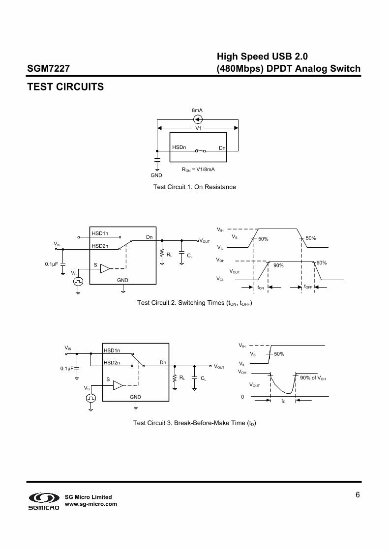
TEST CIRCUITS
V1
8mA
RON = V1/8mA
HSDn Dn
GND Test Circuit 1. On Resistance
VS
VOL
tON tOFF
50% 50%
90% 90%VOH
VOUTVIS
0.1µF
Dn
GNDVS
RL CL
HSD2n
HSD1n
S
VIH
VIL
VOUT
Test Circuit 2. Switching Times (tON, tOFF)
VIS
0.1µFDn
GND
RL CL
VOUTHSD2n
VS
HSD1n VS
VIH
50%
90% of VOH
VIL
0
VOUT
tD
SVOH
Test Circuit 3. Break-Before-Make Time (tD)
High Speed USB 2.0 SGM7227 (480Mbps) DPDT Analog Switch
7SG Micro Limited www.sg-micro.com
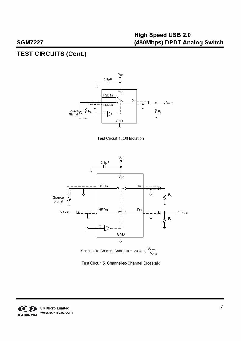
TEST CIRCUITS (Cont.)
VOUTHSD2nDn
GND
S
VCC
SourceSignal
0.1µF
VCCHSD1n
RLRL
Test Circuit 4. Off Isolation
Channel To Channel Crosstalk = -20 × log VHSDn
VOUT
HSDn Dn
VCC
GND
0.1µFVCC
SourceSignal
HSDn Dn
RL
N.C. VOUT
RL
S
Test Circuit 5. Channel-to-Channel Crosstalk
High Speed USB 2.0 SGM7227 (480Mbps) DPDT Analog Switch
8SG Micro Limited www.sg-micro.com
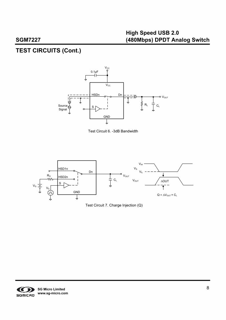
TEST CIRCUITS (Cont.)
VOUTHSDn Dn
GND
S
0.1μFVCC
SourceSignal
VCC
RL CL
Test Circuit 6. -3dB Bandwidth
Dn
GND
SCL
HSD2n
HSD1n
VOUTRG
VG
VIH
VOUT
Q = ΔVOUT × CL
ΔOUT
VIL
VS
VS
Test Circuit 7. Charge Injection (Q)

High Speed USB 2.0 SGM7227 (480Mbps) DPDT Analog Switch
9SG Micro Limited www.sg-micro.com
APPLICATION NOTES Meeting USB 2.0 VBUS Short Requirements Power-Off Protection For a VBUS short circuit the switch is expected to withstand such a condition for at least 24 hours. The SGM7227 has specially designed circuitry which prevents unintended signal bleed through as well as guaranteed system reliability during a power-down, over-voltage condition. The protection has been added to the common pins (D+, D-). Power-On Protection The USB 2.0 specification also notes that the USB device should be capable of withstanding a VBUS short during transmission of data. This modification works by limiting current flow back into the VCC rail during the over-voltage event so current remains within the safe operating range.

High Speed USB 2.0 SGM7227 (480Mbps) DPDT Analog Switch
10SG Micro Limited www.sg-micro.com
SGM7227 USB2.0 Signal Quality Compliance Test Results Figures 1 and 2 show the test results for USB eye diagram tests.
Figure 1. Waveform Plot
Figure 2. High Speed Signal Quality Eye Diagram Test (V+ = 3.3V)
High Speed USB 2.0 SGM7227 (480Mbps) DPDT Analog Switch
11SG Micro Limited www.sg-micro.com
The following is a summary of the USB test Results. The SGM7227 passes the high speed signal quality, eye diagram and jitter tests. Required Tests
Overall result: Pass!
Signal eye: Eye passes
EOP width: 7.91 bits EOP width passes
Measured signaling rate: 480.0551 MHz Signal rate passes
Rising Edge Rate: 901.28 V/us (710.10 ps equivalent risetime) Passes
Falling Edge Rate: 889.18 V/us (719.77 ps equivalent risetime) Passes
Additional Information
Consecutive jitter range: -61.770 ps to 39.668 ps, RMS jitter 21.900 ps Paired JK jitter range: -47.800 ps to 42.890 ps, RMS jitter 21.591 ps Paired KJ jitter range: -50.590 ps to 49.704 ps, RMS jitter 23.281 ps

High Speed USB 2.0 SGM7227 (480Mbps) DPDT Analog Switch
12SG Micro Limited www.sg-micro.com
PACKAGE OUTLINE DIMENSIONS MSOP10
b
E1 E
e
D
A1
L
c
A
A2
θ
Dimensions In Millimeters
Dimensions In Inches Symbol
Min Max Min Max A 0.820 1.100 0.032 0.043
A1 0.020 0.150 0.001 0.006 A2 0.750 0.950 0.030 0.037 b 0.180 0.280 0.007 0.011 c 0.090 0.230 0.004 0.009 D 2.900 3.100 0.114 0.122 E 2.900 3.100 0.114 0.122
E1 4.750 5.050 0.187 0.199 e 0.500 BSC 0.020 BSC L 0.400 0.800 0.016 0.031 θ 0° 6° 0° 6°

High Speed USB 2.0 SGM7227 (480Mbps) DPDT Analog Switch
13SG Micro Limited www.sg-micro.com
PACKAGE OUTLINE DIMENSIONS UTQFN1.8×1.4-10L
TOP VIEW BOTTOM VIEW
SIDE VIEW
1.800 ±0.050
1.40
0 ±
0.05
0
PIN #1 DOT BY MARKING
0.400 ±0.050(×9)
0.400 TYP
0.50
0±0.
050 0.200±0.050
0.800 REF
PIN #1 IDENTIFICATION CHAMFER 0.100×45°
0.55
0±0.
050
0.00
0-0.
050
0.152 REF
NOTE: All linear dimensions are in millimeters.
REV. A
SGMICRO is dedicated to provide high quality and high performance analog IC products to customers. All SGMICRO products meet the highest industry standards with strict and comprehensive test and quality control systems to achieve world-class consistency and reliability. For more information regarding SGMICRO Corporation and its products, please visit www.sg-micro.com