servicing the kl400meirion-ars.info/wp-content/uploads/2013/12/servicing-the-kl400.pdf · page 2 of...
TRANSCRIPT

Page 1 of 20
REPAIRING THE
RM KL400 LINEAR AMPLIFIER.
Les Carpenter G4CNH December 2012

Page 2 of 20
The following is a step by step guide to fixing your KL400 amplifier. Each part will be individually tested up to the final output stage, which should there still be no RF output, can then be considered to have probable output transistor failure. A simple test is provided that may prove a failure in one or both output transistors. You will need a soldering iron, cross head screwdriver, tweezers or fine pointed nose pliers, a CB rig with 4 Watts of out put and a suitable 150W dummy Load. A solder removing tool or Wick is also recommended. Additionally, you may require an instrument screwdriver to loosen the grub screw on the power control knob and a suitable box spanner for the switch itself. To power up the completed amplifier you will also need either a fully charged car battery or a 12V power supply capable of giving around 20 Amps. However during the early stages of fault finding, a 12V power supply with variable current limiting is recommended. Set initially to something like 250mA this can help prevent damage due to various fault conditions. Remove two screws that secure rear cover and place all three items into a suitable storage container for safe keeping. You should now be able to slide off the bottom plate. Remove two screws from each coax socket. Remove four screws securing front panel. Remove four Black and five Silver screws as shown below:-

Page 3 of 20
Carefully extract circuit board complete with front panel and both coax sockets, taking care that you do not bend the front panel away from its 90 degrees with the circuit board as this may cause broken connections. Take care with this during the test routines that follow. Also check that the mica washer associated with TR5 is safely retained on the heatsink. If it has come loose then carefully retrieve and place in storage container. Using a soldering iron, remove L6, L7 and disconnect earthy end of T2 primary:- Reason: Removing L6 isolates PA Bias Supply, removing L7 isolates 12V from the final transistors and removing ground wire from T2 isolates the DC control switch to allow DC testing of the Power switch board and its associated components.

Page 4 of 20
1st Test: Check with a Multimeter that there is continuity between the two coax socket inners. This proves circuit board continuity and one half of the contact sets on RL1 and RL2. 2nd Test: Lift one end of each of the fuses and check they have continuity. Replace fuses back into their clips. 3rd Test (Pre-Amp) An easy way to check the pre-amp is to connect a rig (squelch off) to the RIG coax socket on the Amplifier (Top right socket with front panel to the left). Because this socket no longer has an earth connection, make a temporary link between the coax connector body and the ground plane earth of the circuit board. A short length of wire tacked onto the ground plane with a crocodile clip connected to the socket would be ideal though the author has used just a screwdriver to make the connection as the test is very brief. Set PRE switch to OFF, AMP switch to OFF and SSB/AM switch to AM. Place the linear circuit board on a suitable insulated surface and apply the12V supply. Check that after setting the PRE switch to ON, the PRE LED illuminates (Proves S1, R9 and the LED D11). The Relay RL1 should be heard to operate (Proves TR2, the Relay, R3 and R4). The noise level should be heard to increases on the monitoring rig (Proves TR8 and the circuitry around it including the other contact position of RL1). 4th Test (RF sensor and AM/SSB switch) Briefly key up rig a few times and check RL1 clicks (Proves TR1, R1, D1, D2, C3 and C5). Note that there should be a very slight delay after de-keying which proves C8. Set the SSB/AM switch to SSB and verify that the delay is longer. (Proves switch S3 and C9) Set linear PRE to OFF. Remove 12V from board under test.

Page 5 of 20
5th Test (Power Control) Apply 1 Volt to the power switch wiper A and monitor the output using a Multimeter and DC Test Circuit as shown below:-. (Note a 1.5V cell can suffice but expect slightly higher voltages)
This should have proved Power Control Switch, R17, R18, R19, R20, R21 and R22. Remove DC Test Circuit and Multimeter. If you found some switch positions faulty then it is highly likely that one of the attenuator resistors mounted on the switch board is faulty. A common failure is an open circuit 10 Ohm resistor R19. If all is OK then go to 6th Test else follow the instructions below. If you cannot gain easy access to a faulty resistor on the power control board, then it may have to be removed. Remove the board by first loosening the power control knob grub screw and pulling off the knob. Using a suitable box spanner or equivalent, remove the switch fixing nut, shake proof and plain washers. Unsolder the pads of the switch board from those on the main board; a solder removing tool is a good thing to have for this operation. Carefully remove switch from the front panel taking care not to allow the switch indent tabbed washer to fall out, this sets the number of switch positions (i.e. six). It is a good idea to temporarily replace the switch fixing nut to hold the indent tabbed washer in position but don’t worry if it has fallen out, as its correct position can easily be found later. Just don’t loose the tabbed washer!

Page 6 of 20
Set the switch fully anti-clockwise (Position 1) and using the Multimeter, check across each of the resistors for the values shown with no more than 5% error. Expect the 10 Ohm resistors to be between 9.5 and 10.5 Ohms, the 27 Ohm resistor to be between 25.6 and 28.3 Ohms, the 47 Ohm resistor to be between 44.6 and 49.3 Ohms and the 100 Ohm resistor between 95 and 105 Ohms. Replace as necessary. Now if you dislodged the indent washer, simply refit to the switch with the tab on the washer located in one of the slots. Turn the switch from position 1 and count 2, 3, 4, 5, 6 before the switch rotation stops. If you have too many or too few stops, reset switch to position 1, relocate the tab on the washer to another slot and repeat until all six positions can be made. Carefully replace the switch into the front panel and secure with the nut and washers previously removed, making sure the indent washer does not fall out while you are doing it! Now hold the two boards together at 90 degrees and reflow solder onto the three pads. Replace the knob and tighten the grub screw when the knob pointer indicates correctly on the front panel markings.
Page 7 of 20
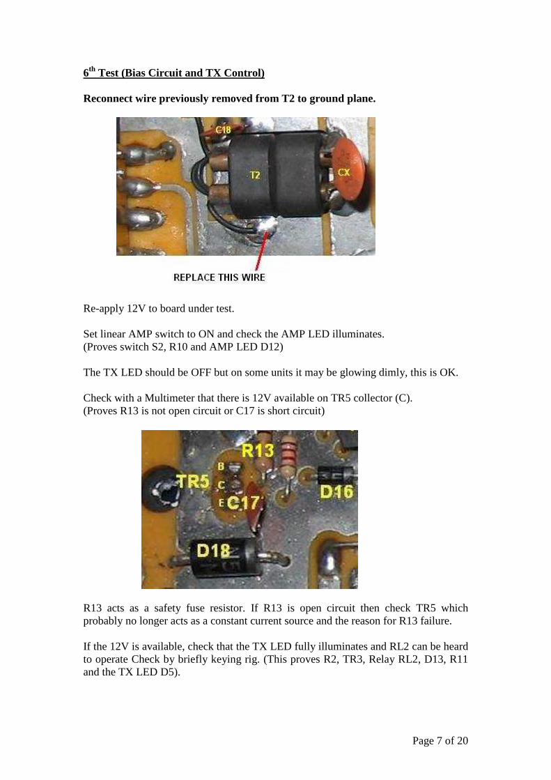
6th Test (Bias Circuit and TX Control) Reconnect wire previously removed from T2 to ground plane.
Re-apply 12V to board under test. Set linear AMP switch to ON and check the AMP LED illuminates. (Proves switch S2, R10 and AMP LED D12) The TX LED should be OFF but on some units it may be glowing dimly, this is OK. Check with a Multimeter that there is 12V available on TR5 collector (C). (Proves R13 is not open circuit or C17 is short circuit)
R13 acts as a safety fuse resistor. If R13 is open circuit then check TR5 which probably no longer acts as a constant current source and the reason for R13 failure. If the 12V is available, check that the TX LED fully illuminates and RL2 can be heard to operate Check by briefly keying rig. (This proves R2, TR3, Relay RL2, D13, R11 and the TX LED D5).
Page 8 of 20
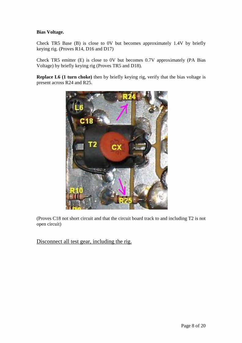
Bias Voltage. Check TR5 Base (B) is close to 0V but becomes approximately 1.4V by briefly keying rig. (Proves R14, D16 and D17) Check TR5 emitter (E) is close to 0V but becomes 0.7V approximately (PA Bias Voltage) by briefly keying rig (Proves TR5 and D18). Replace L6 (1 turn choke) then by briefly keying rig, verify that the bias voltage is present across R24 and R25.
(Proves C18 not short circuit and that the circuit board track to and including T2 is not open circuit) Disconnect all test gear, including the rig.

Page 9 of 20
7th Test (RL2 second contact position) This is the final test to be done with the board out of its heatsink enclosure and is highly recommended as faults in this area have been commonly found. It is necessary to force RL2 to operate without any RF coming from the rig (which you should have removed in the last instruction). The easiest way to make RL2 operate is to apply a short link wire between the ground plane and the anode of D6.
Now these tests have to be done as briefly as possible because TR5 is not mounted to the heatsink case and will get hot very quickly! Apply 12V supply and verify that RL2 operates and the TX LED illuminates, switch off the 12V supply. Using the Multimeter as a continuity tester, connect it between the inner of the RIG coax socket (Top right with front panel to your left) and the power control board input pad. This is the pad used in the 4th Test where the 1V test voltage was applied.
Page 10 of 20
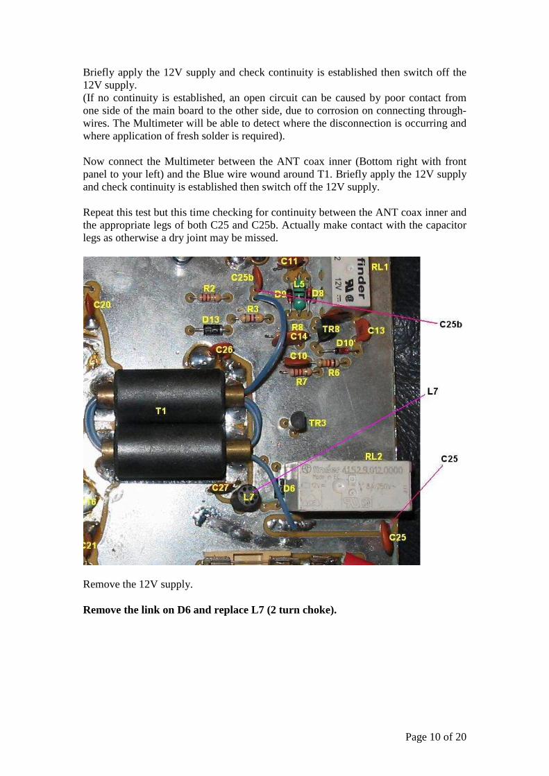
Briefly apply the 12V supply and check continuity is established then switch off the 12V supply. (If no continuity is established, an open circuit can be caused by poor contact from one side of the main board to the other side, due to corrosion on connecting through-wires. The Multimeter will be able to detect where the disconnection is occurring and where application of fresh solder is required). Now connect the Multimeter between the ANT coax inner (Bottom right with front panel to your left) and the Blue wire wound around T1. Briefly apply the 12V supply and check continuity is established then switch off the 12V supply. Repeat this test but this time checking for continuity between the ANT coax inner and the appropriate legs of both C25 and C25b. Actually make contact with the capacitor legs as otherwise a dry joint may be missed.
Remove the 12V supply. Remove the link on D6 and replace L7 (2 turn choke).

Page 11 of 20
Visually check out R23/C20 and R26/C21 to ensure they do not have any dry joints.
Re-assemble board into chassis taking care that the mica washer for TR5 is in place. The author likes to add a small drop of Electrolube HTC Plus heat sink compound to the three heatsink positions where TR5 and the Output Transistors are secured. With a suitable dummy load attached to the linear output ANT socket, apply a rig to the RIG socket and key up with the POWER CONTROL at position 1 and AMP switched ON. Unit should be operating and increase in output power as the POWER CONTROL is advanced to position 6. With 4 Watts input you should get in excess of 100 Watts. If there is no or little RF output, confirm that there is a substantial increase of 12V supply current as the POWER CONTROL switch is advanced. This proves drive is present on the output devices and they are working. If there is no increase in supply current then suspect failure of the output transistors TR6 and TR7 or a missed dry joint around the final stage circuitry.
Page 12 of 20
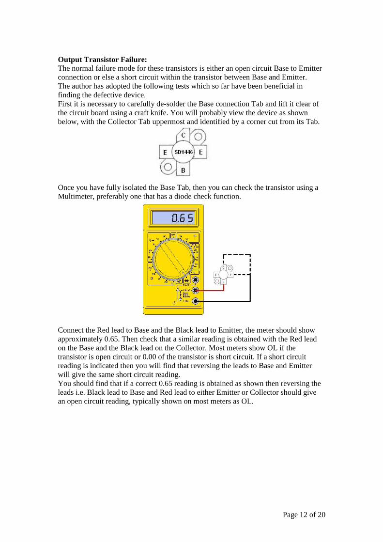
Output Transistor Failure: The normal failure mode for these transistors is either an open circuit Base to Emitter connection or else a short circuit within the transistor between Base and Emitter. The author has adopted the following tests which so far have been beneficial in finding the defective device. First it is necessary to carefully de-solder the Base connection Tab and lift it clear of the circuit board using a craft knife. You will probably view the device as shown below, with the Collector Tab uppermost and identified by a corner cut from its Tab.
Once you have fully isolated the Base Tab, then you can check the transistor using a Multimeter, preferably one that has a diode check function.
Connect the Red lead to Base and the Black lead to Emitter, the meter should show approximately 0.65. Then check that a similar reading is obtained with the Red lead on the Base and the Black lead on the Collector. Most meters show OL if the transistor is open circuit or 0.00 of the transistor is short circuit. If a short circuit reading is indicated then you will find that reversing the leads to Base and Emitter will give the same short circuit reading. You should find that if a correct 0.65 reading is obtained as shown then reversing the leads i.e. Black lead to Base and Red lead to either Emitter or Collector should give an open circuit reading, typically shown on most meters as OL.

Page 13 of 20
Brief circuit description. (This is for the more common alternative circuit) With all switches OFF, the signals arriving at the ANT socket are routed to the RIG socket via two contacts in RL2 and two contacts in RL1.If the PRE switch is set to ON, the PRE LED illuminates with R9 providing current limit for the LED at approximately 10mA. Relay RL1 operates due to its driving transistor TR2 being turned on by forward bias current supplied by R3 and R4, TR1 at this time is turned off. D7 is a back stop diode to prevent damage to TR2 when the relay is de-energised. The first contact set of the relay switches the input signal to the base of TR8 via D10 and C13. D10 is forward biased by R6 and applies approximately 1.7V to the base of TR8 by the action of the diode and potential divider formed with R7. The transistor amplifies the input signal with the output developed across choke L5 which is coupled to the rig via C12 and the second contact set of RL1. Diodes D8 and D9 would appear to limit the signal being developed across the choke in situations where there is a strong local transmission being received. However we shall see later that they perform an even more important duty. If the rig is keyed up at this time then some of the 4 Watts input at the rig socket is taken via C3 to D1 and D2. D1 removes the negative going excursion of this sampled signal whilst D2 rectifies the positive going excursion and charges C8. C5 removes any high frequency 27MHz carrier signal at this point. The positive DC voltage developed across C5 is used to bias ON the transistor TR1 with R1 acting as a series limiter to prevent excess base to emitter current flow within TR1. TR1 having turned ON, effectively grounds the base of TR2, starving it of base current and turning TR2 OFF. Relay RL1 will now de-energise to switch the preamp out of circuit such that the rig output can now go direct to the ANT socket via the contacts of RL2. Note that there is a slight delay by the relay RL1 in doing this so the full 4 Watts of rig power will be present on C12 for a short time. This is where the diodes D8 and D9 come into play again, by limiting the amount of RF signal briefly appearing on the transistor TR8. If the AMP switch S2 was switched ON, then a number of things will have taken place. 1) A positive supply will now be applied to the AMP LED with R10 acting as a current limiter for the LED. 2) A positive supply will now be applied to RL2 via diode D13. 3) A positive supply will now be applied to the bias supply transistor TR5. With the rig un-keyed, RL2 cannot energise due to TR3 being turned OFF, TR4 will be turned ON thus turning OFF the bias supply transistor. When the rig is keyed, TR3 will turn ON and activate RL2, TR4 is turned OFF thus allowing the bias supply transistor TR5 to turn ON. This transistor has its Base held by two diode drops provided by D16 and D17 (approximately 1.4V). Because of the 0.7V drop across the Base/Emitter junction of this transistor, the actual voltage fed to the bases of the output transistors will be approximately 0.7V also. To protect the output transistors from damage due to a short circuit TR5, there is a clamping diode D18. L6 and C10 provide HF decoupling from any RF that may be fed back from the centre tap of T2. When RL2 operated, its contact set shown as ‘b’ would have switched the Antenna socket to the power amp tank coil T1. At the same time, the contact set ‘a’ would direct the 4 watt rig output to the power control switch S4. This is a 6 position

Page 14 of 20
attenuator feeding the transformer T2 which supplies RF to the bases of the output transistors TR6 and TR7. Being a centre tapped transformer, the signals to the transistors will be in anti-phase for push-pull operation. Note that the output transistors are continuously supplied with 12V supply from the main fuses then via L7. It is the absence or presence of the bias supply that makes these transistors conduct so its operation is critical for amplifier operation.

Page 15 of 20
Original KL400 circuit diagram that used two RF sensor circuits.

Page 16 of 20
Original two RF sensor model - layout
Page 17 of 20
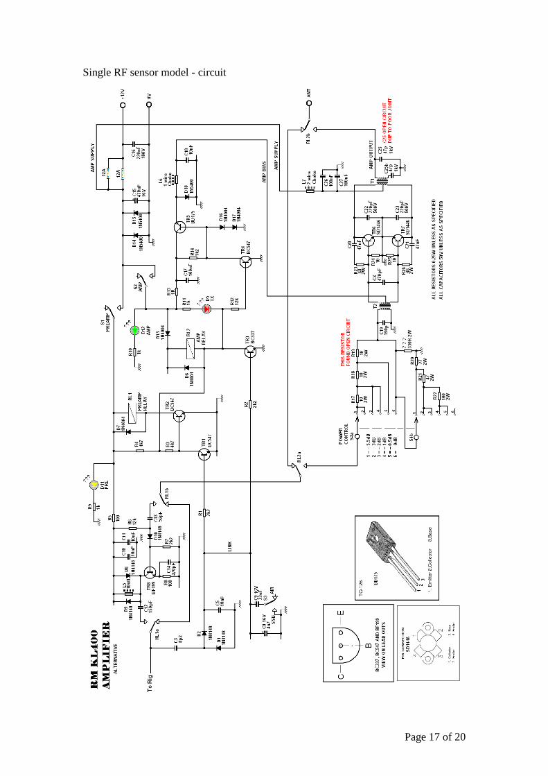
Single RF sensor model - circuit

Page 18 of 20
Single RF sensor model - layout
Note how the resistors R15 and R16 have been removed and the drive now goes directly into the power control board via a circuit pad underneath. This may have been done to cater for 4 Watt output UK rigs as the additional attenuation may have been intended to handle higher inputs, e.g. 10 Watts, from continental rigs. It is a puzzle why the 330 Ohm resistor has been added on the power control output pad. If you look closely to the left of C9 (middle of board – far left) you will see the wire link that connects TR1 and TR3 to a common single RF sensor.

Page 19 of 20
Another slightly different single sensor model – circuit

Page 20 of 20
Another slightly different single sensor model – layout
It is possible that the 4k7 resistor shown lower right hand side which connects with R11 was added to stop the dim glow of the TX LED when the AMP switch is set to ON and the driving rig is not keyed up. Note also that R15 and R16 have also been removed so the drive goes directly into the power control board. However it is the input pad this time that has a 390 Ohm resistor and 47pF capacitor added.