series - wegecatalog.weg.net/files/wegnet/1-17276.pdf · chapter 4 keypad (hmi) ... 4=p010 5=p042...
TRANSCRIPT


Series: CFW-09RBSoftware: version 1.2X0899.4789 E/5
REGENERATIVE
CONVERTER
MANUAL
ATTENTION!
It is very important to check if the
inverter software is the same as
indicated above.
04/2004

Summary of Revisions
The Table below describes all revisions made to this Manual.
Revision Description Pages
1 First Edition -2 Change pre-charge 23 Inclued currents up 600A 54 Change RL 1 software-programming 5

Table of Contents
Quick ParameterReference, Fault and
Status Messages
1 Parameters .............................................................................. 052 Fault Messages ....................................................................... 093 Other Messages ...................................................................... 09
CHAPTER 1General Information
1.1 About this Manual .................................................................... 101.1.1 Harmonics....................................................................... 101.1.2 Braking ........................................................................... 181.1.3 Application ...................................................................... 21
1.2 CFW-09RB Simplified Block Diagram ...................................... 24
CHAPTER 2Electrical Installation
2.1 European EMC Directive .......................................................... 27
CHAPTER 3Start-up
3.1 Pre-Power Checks ................................................................. 283.2 Initial Power-up ...................................................................... 28
CHAPTER 4Keypad (HMI) Operation
4.1 Description of the CFW-09RB-LCD Keypad .............................. 304.2 Use of the Keypad (HMI) .......................................................... 31
4.2.1 Use of the Keypad (HMI) ................................................. 324.2.2 Signalling/Indication on the HMI Displays ........................ 32
4.3 Parameter Programming .......................................................... 334.3.1 Parameter Selection/Programming .................................. 33
CHAPTER 5Detailed Parameter Description
5.1 Access and Read Only Parameter - P000...P099 .................... 355.2 Regulation Parameters - P100...P199 ...................................... 385.3 Configuration Parameters - P200...P399 .................................. 40
CHAPTER 6Diagnostics and Troubleshooting
6.1 Faults and Possible Causes .................................................... 47

Table of Contents
CHAPTER 7Technical Characteristics
7.1 Power Data ......................................................................... 507.1.1 220 - 230V Power Supply .......................................... 507.1.2 380 - 480V Power Supply .......................................... 50
APPENDIX ASwitching Frequency Filter
..................................................................................................... 52
APPENDIX BCFW-09RB Line Reactor
..................................................................................................... 53

CFW-09RB - QUICK PARAMETER REFERENCE
5
QUICK PARAMETERREFERENCE, FAULT ANDSTATUS MESSAGES
Software: V1.2XApplication:Model:Serial Number:Responsible:Date: / / .
1. Parameters
Parameter Description Adjustable RangeFactory User´s
PageSetting SettingP000 Parameter Access 0...999 0 35
Read Only Parameters LEITURA P001 ... P099P002 Line Voltage 0...600 35P003 Input Current 0...2600 A 35P004 DC Link Voltage 0...1077 V 35
P006 Rectifier Status
rdy
35runSubEXY
P010 Input Power 0.0...1200 kW 35
P012 DI1...DI2 StatusA = Active
36I = Inactive
P013 DO1, DO2, RL1, RL2, RL3 StatusA = Ativa
36I = Inativa
P014 Last Fault E00...E41 36P015 Second Previous Fault E00...E41 36P016 Third Previous Fault E00...E41 36P017 Fourth Previous Fault E00...E41 36P022 WEG use 0%...100% 37P023 Software Version 1.0X 37P025 A/D Iv value 0...1023 37P026 A/D Iw value 0...1023 37P027 WEG use -999...999 37P028 WEG use 0...2100 37P029 WEG use 0...2100 37P042 Time powered 0...65530 h 37P043 Time Enabled 0...6553 h 37
Regulation Parameters P120 ... P199Reactive Current Reference
P121Reactive Current
-100%...100% 0.0% 37ReferenceDC Voltage Regulation
P151
322V...394V (P296=0) 358V
38 556V...680V (P296=1) 618V
DC Voltage Level 585V...715V (P296=2) 650V 646V...790V (P296=3) 718V 695V...825V (P296=4) 750V
Overload CurrentsP156 Overload Current - 100% 0...1.3xP295 1.1xP295 38

CFW-09RB - QUICK PARAMETER REFERENCE
6
Parameter Description Adjustable RangeFactory User´s
PageSetting SettingDC Link Voltage Regulation
P161 Proportional Gain 0.0...63.9 5.0 38P162 Integral Gain 0.000...9.999 0.009 39 Input Current RegulationP167 Proportional Gain 0.00...1.99 0.7 40P168 Integral Gain 0.000...1.999 0.250 40P169 Maximum Braking Current 0...150%xP295 100% (P295) 40P170 Maximum Motoring Current 0...150%xP295 100% (P295) 40
Input Reactive Current regulationP175 Proportional Gain 0.0...31.9 3.3 40P176 Integral Gain 0.000...9.999 0.067 40P179 Maximum Reactive Current 0...120% 120% 40P180 Ractive Generation Point 0...120% 120% 40
CONFIGURATION
Parameters P200 ... P399
P200 Password0=Off
1=On 401=On
P201 Language Selection0=Portuguese
411=English2=Spanish
P204 (1) Load/save Parameters
0=Not used
0 41
1=Not used2=Not used3=Reset P0434=Not used5=Loads factory default
P205 Display Default Selection
0=P002
2=P002 41
1=P0032=P0043=P0064=P0105=P0426=P043
P206 Auto-Reset Time 0...255s 0s 41
P218LCD Display
0...150 127 41Contrast Adjustment
Analog Outputs
P251 Analog Output AO1 Function
0=Line Voltage
0=Line Voltage 421=Input Current2=Link Voltage3=Input Power
P252 Analog Output AO1 Gain 0.000 ... 9.999 1.000 42
P253 Analog Output AO2 Function
0=Line Voltage
0=Line Voltage 421=Input Current2=Link Voltage3=INput Power
P254 Analog Output AO2 Gain 0.000 ... 9.999 1.000 42
P255Analog Output AO3 Function
0=Line Voltage
0=Line Voltage 42(Requires optional I/O expansion
1=Input Current2=Link Voltage3=INput Power
board EBA or EBB More than 21 signals forexclusive WEG use
To be definedby the user

CFW-09RB - QUICK PARAMETER REFERENCE
7
P256 Analog Output AO3 Gain 0.000 ... 9.999 1.000 42
P257Analog Output AO4 Function
0=Line Voltage
0=Line Voltage 42(requires optional I/O expansion
1=Input Current2=DC Link Voltage
board EBA or EBB) 3=INout PowerMore than 21signals forexclusive WEG use
P258 Analog Output AO4 Gain 0.000 ... 9.999 1.000 42
Digital InputsP263 (1) Digital Input DI1 Function 2=General Enable 2=General Enable 43P264 (1) Digital Input DI2 Function 4=Without external Fault 4=Without ext. Fault 43
Saídas Digitais
P275 (1)Output DO1 Function
0...10=Not used
0=Not used 44(requires opr=tional I/O expansion
11=run12=ready13=No Fualt14=No E0015=No E01+E02+E03
board EBA or EBB) 16=No E0417=No E0518...23=Not used24=Preload OK25=With fault26=Not used
P276 (1)Output DO2 Function
0...10=Not used
0=Not used 44(requires optional I/O expansion
11=run12=ready13=No fault14=No E0015=No E01+E02+E03
Board EBA or EBB) 16=No E0417=No E0518...23=Not used24=Preload OK25=With Fault26=Not used
P277 (1) Relay RL1 Function
0...10=Not used
24=Preload OK 44
11=run12=ready13=No fault14=No E0015=No E01+E02+E0316=No E0417=No E0518...23=Not used24=Preload OK25=No fault26=Not used
Parameter Description Adjustable RangeFactory User´s
PageSetting Setting

CFW-09RB - QUICK PARAMETER REFERENCE
8
Parameter Description Adjustable RangeFactory User´s
PageSetting Setting
P279 (1) Relay RL2 Function
0...10=Not used
13=No fault 44
11=run12=ready13=No fault14=No E0015=No E01+E02+E0316=No E0417=No E0518...23=Not used24=Preload OK25=No fault26=Not used
P280 (1) Relay RL3 Function
0...10=Not used
11=run 44
11=run12=ready13=No fault14=No E0015=No E01+E02+E0316=No E0417=No E0518...23=Not used24=Preload OK25=Wiuth fualt26=Not used
Rectifier Data
P295 (1) Rated Current
17=86.0A
45
18=105.0A19=130.0A20=142.0A21=180.0A22=240.0A23=361.0A24=450.0A25=600.0A26=650.0A27=810.0A28=1080.0A29=1215.0A30=1620.0A
P296 (1) Rated Voltage
0=220V/230V
461=380V2=400V/415V3=440V/460V4=480V
P297 (1) Switching Frequency1=2.5 kHz
2=5.0 kHz 462=5.0 kHz
According to therated rectifier current
According to therated rectifier voltage
(1) Parameters can be changed only when rectifier is disabled

CFW-09RB - QUICK PARAMETER REFERENCE
9
Display Description Page
E00 Overcurrent at the Input 47E01 DC Link Overvoltage 47E02 DC Link Undervoltage 47E03 Power Supply Undervoltage/Phase Loss 48
E04(*)Inverter Overtemperature/Pre-charge Circuit Failure
E05 Output Overload ( Ixt function) 48E06 External Fault 48E08 CPU Error (watchdog) 48E09 Program Memory Error 48E16 Line Overvoltage 48E31 Keypad Connection Fault 48E41 Self-Diagnosis Fault 48
2. Fault Messages
(*) O E04 can be “Preaload Circuit Fault" only for the following models:86A/105A/142A (380V-480V) e 70A/ 86A/105A/130A (220V-230V).
3. Other Messages Display Description
rdy Rectifier is ready to be Enabledrun Rectifier is Enabled
SubRectifier with too low Voltage for Inverter Operation
(undervoltage)
10
GENERAL INFORMATION
This purpose of this Manual is to provide information about the CFW-09RB regenerative converter. Before reading this manual, read the CFW-09 Frequency Inverter Manual. All information regarding Safety Notices,Version of Software, Nameplate, Receiving and Storing, MechanicalInstallation and Warranty Terms described in that Manual should alsobe considered for this rectifier line.
CHAPTER 1
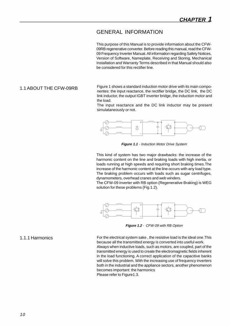
1.1 ABOUT THE CFW-09RB Figure 1 shows a standard induction motor drive with its main compo-nentes: the input reactance, the rectifier bridge, the DC link, the DClink inductor, the output IGBT inverter bridge, the induction motor andthe load.The input reactance and the DC link inductor may be presentsimulataneously or not.
Figure 1.1 - Induction Motor Drive System
This kind of system has two major drawbacks: the increase of theharmonic content on the line and braking loads with high inertia, orloads running at high speeds and requiring short braking times.Theincrease of the harmonic content at the line occurs with any load type.The braking problem occurs with loads such as sugar centrifuges,dynamometers, overhead cranes and web winders.The CFW-09 inverter with RB option (Regenerative Braking) is WEGsolution for these problems (Fig.1.2).
Figure 1.2 - CFW-09 with RB Option
1.1.1 Harmonics For the electrical system sake , the resistive load is the ideal one.Thisbecause all the transmitted energy is converted into useful work.Always when inductive loads, such as motors, are coupled, part of thetransmitted energy is used to create the electromagnetic fields inherentin the load functioning. A correct application of the capacitive bankswill solve this problem. With the increasing use of frequency invertersboth in the industrial and the appliance sectors, another phenomenonbecomes important: the harmonicsPlease refer to Figure1.3.

GENERAL INFORMATION
11
FigurE 1.3 - Complex Wave Form
It seems to be a sine wave with large distortion. Through the mathematicsone can prove that the signal from Fig. 1.3 is formed by the sum of severalsive waves of different frequencies and amplitudes. (Fig. 1.4).
Figure 1.4 - Harmonic Decomposition of the signal of the Figure 1.3.
By analyzing the Fig. 1.4, one can note that there is a sine wave of largerampltitude, known as fundamental harmonic or first harmonic.In this case it has a peak value equal to 100 and a frequency of 60 Hz.Other sine waves (harmonics) are analysed relating to the fundamentalharmonic: one of theses waves has a peak of 20 Volts (or 20% of thefundamental) and a frequency of 300 Hz (five times the fundamental,therefore the name fifth harmonic): the other wave has a peak of 14 Volts(approx. 14% of the fundamental) and a frequency of 420 Hz (seven timesthe fundamental, thus the seventh harmonic). One can say that the morecomplex the signal, more harmonics form this signal, i.e., there can bepresent the eleventh harmonic, the thirteenth hamonic and so on.There are also even harmonics (second, fourth, etc.), but in a general waythese harmonics are not present in the signals of our interest or they havea very low value.The diode rectifiers operate in such a way that the line energy is transferredonly to the output capacitor bank when the line voltage is higher than thecapacitor bank voltage. Therefore the current drained by the rectifier brid-ge is pulsed.

GENERAL INFORMATION
12
Figure 1.5 - Wave Form of the Phase Voltage and the Input Current of aThree-Phase Diode Bridge.
The rectifier input current harmonics have been extensively studiedand it is known that the harmonic order is given by the followingformula:
η = P . k ± 1
where k can assumes values as 1, 2, 3...and P is the number of pul-ses of the rectifier bridge.A complete three-phase bridge has 6 pulses, thus P=6. 5th , 7th, 11th,etc. harmonics will be present. Thus in a single-phase bridge P=2 andwe will have additionally the third harmonic. Consequently in a bridgewith twelve pulse we won´t have the third, the fifth and the seventhharmonics.Which will be the problem when we have a high harmonic content inthe input current? The problem will be that only the first harmoniccontributes to the energy transference between the source and theload, i.e., only this harmonic produces a useful work. The otherharmonics will produce only losses in the system, causing overheatingon equipment such as generators and transformers.Thus in order tocompensate this effect, the equipment must be oversized, andconsequently increasing the end costs. Figure 1.6 shows another effectof these harmonics: the current drained by the non-linear load (in thiscase, the rectifier) has harmonics that produces proportional systemimpedance drops, causing harmonics in the line voltage that suppliesthe motor. Also the motor will drain a current with some harmoniccontent. Besides this distorted supply will generate an additional mo-tor overheating. Although the figure shows only one motor as linearload, we must consider that this load may be in the same installationor even in adjacent factories.
Figure 1.6 - Effects of the harmonics in the system
(1)
Current
Voltage
Motor
Non-linear loadDistorted Voltage

GENERAL INFORMATION
13
Although we had discussed only uncontrolled rectifier bridges, we cansay that the effects of thyristor bridges are very similar. The main differenceis as the triggering angle increases the delay between the voltage and thefundamental component of the input current also increases . To considerthe harmonic effects in the system, a new concept of power factor had tobe developed. In the past, when the loads were only capacitive, inductiveand resistive, the power factor was defined as the cosine of the anglebetween the voltage and the current. This angle is measured consideringthat the period of the voltage of a 60 Hz line is a little more than 16 ms,corresponding to 360 degrees. Fig. 1.7a shows a voltage advanced insome milliseconds relating to the current. The circuit is inductive and thecosine of the angle converted from milliseconds to grades is positive andsmaller than 1. Fig. 1.7b shows a current advanced relating to the voltageThe circuit is capacitive and the cosine of the angle is smaller than zeroand larger than a negative value. If this circuit would be only resistive, thevoltage would be in phase with the current, providing an angle equal tozero and a cosine equal to 1.
Figure 1.7 - Inductive and Capacitive Circuit
This former power factor has been redifined as displacement factor. Thisdifference is that in this new factor the angle is measured between thefundamental of the voltage and the fundamental of the current.To consider the harmonic content of the current, another factor, designatedas harmonic current distortion rate, has been created.This factor is calculated by adding the rms value of all harmonics afterthat extracting the square root of this sum and dividing the result by thefundamental rms value.
TDH (Ι)% = ∑
h 2 Ι
2 h
Ι1
(2)
Formula 3 shows how are combined the displacement factor and theharmonic current distortion rate in the new power factor definition:
FP = Cos φ1
1 + TDH2 (3)
a
b
Voltage
Voltage
Current
Current

GENERAL INFORMATION
14
The method selection to minimize the harmonic content dependsbasically on the costs and the standards that have to be met. Thestandards change from country to country and the distortion levels aregenerally established according to the involved power or according tothe effects on the system. There are even some standards about EMCthat deal with this subject. One of the most used method is theintroduction in the supply of a serial inductance, also know as linereactance. This line reactance is generally specified according to thepercentual line voltage drop. As the inductance increases, thetransference of the line energy to the capacitor bank will become lessabrupt, thus resulting in smaller current pulse amplitudes andconsequently decreasing the harmonic content. As the reactancesgenerate drops higher than 4%, there will no be a perceptible effect(Fig. 1.8). Through this method it is possible to obtain distortion ratesin the order of 39%.
Figure 1.8 - Currents with Input Reactance
Another applied method adds an inductor in the inverter DC link. Theeffects are the same, but the shape of the input current wave is slightdifferent (Fig. 1.9).
Figure 1.9 - Input Current with Inductor in the Link
There are advantages and disadvantages by applying these methods.The line reactance reduces the rms current of the diodes on the rectifierbridge, reduces the current ripples in the capacitor of the DC link circuit(thus increasing their useful life) and delimits the “notches” area,

GENERAL INFORMATION
15
Figure 1.10 - A “NOTCH”
Figure 1.11 - Close to a NOTCH
The line reactance also reduces the effects of the line voltage peaks onthe inverter. These peaks cause a locking due to overvoltages in the DClink. The disadvantages of the line reactance are the volume and the dropin the average voltage of the inverter DC link, thus limiting the maximumvoltage of the driven motor and consequently its torque.The link inductor has a smaller volume and does not cause drop in theaverage DC link voltage, but it does not have the same limiting effect of theline peaks, when compared with the line reactance. The link inductorpromotes the introduction of “notches” in the line, as well as producesundesired oscillations due to resonances with elements of the system.Another solution is the association of rectifiers to obtain a higher numberof pulses (12, 18 and 24 pulses, higher numbers are less usual). Themost used solution is the configuration for 12 pulses that may have therectifier bridges series or parallel conected. In addition, these bridges canbe of controlled or uncontrolled type.
caused by transitory short-circuits in the electric network during thecommutation of the diodes with different arms in the rectfier bridge. These“notches” are deformations in the line voltage which depth and area areregulated by some standards. (Fig. 1.10 and 1.11).
GENERAL INFORMATION
16
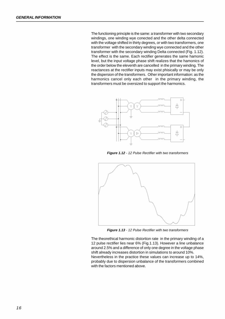
Figure 1.12 - 12 Pulse Rectifier with two transformers
Figure 1.13 - 12 Pulse Rectifier with two transformers
The theorethical harmonic distortion rate in the primary winding of a12 pulse rectifier lies near 6% (Fig.1.13). However a line unbalancearound 2.5% and a difference of only one degree in the voltage phaseshift already increases distortion in simulations to around 10%.Nevertheless in the practice these values can increase up to 14%,probably due to dispersion unbalance of the transformers combinedwith the factors mentioned above.
The functioning principle is the same: a transformer with two secondarywindings, one winding wye conected and the other delta connectedwith the voltage shifted in thirty degrees, or with two transformers, onetransformer with the secondary winding wye connected and the othertransformer with the secondary winding Delta connected (Fig. 1.12).The effect is the same. Each rectifier generates the same hamoniclevel, but the input voltage phase shift realizes that the hamonics ofthe order below the eleventh are cancelled in the primary winding. Thereactances at the rectifier inputs may exist phisically or may be onlythe dispersion of the transformers. Other important information: as theharmonics cancel only each other in the primary winding, thetransformers must be oversized to support the harmonics.

GENERAL INFORMATION
17
Ano ther solutions can be adopted to solve this problem. All this solutionsintroduce some device that is serial or parallel conected to the rectifiersupply. Among these solutions are low-pass filters combined withtransformers and capacitors connected in series with the line. These filtersresults in distortion rates in the range from 8 to 10% and power factors inthe order of 0.9 to 0.95.Another solution is the application of an active filter,another kind of con-verter connected at the inverter input. This converter absorbs to someextent the harmonic content that is generated by the rectifier. With thissolution distortion rates in the order of 4% can be achieved, but this solutionis very expensive.Also filters tuned to a serial harmonic and producing significant reductionat that hamonic can be used, but this alternative will also generate asignificant drop of the average voltage in the DC link. The tuned filter canbe also connected parallel to the supply, but here they can generateoscillations due to the resonance with other elements of the system.Another additional undesirable effect can be generated: as the filter offersto the harmonics a path of low impedance, it can drain the harmonicsfrom a nearby factory, for instance, producing filter overload. To minimizethese effects, you must add a serial reactance.But this solution will increase still more the costs of the installation thatare already high.Fig. 1.14 shows the main components of a CFW-09 RB drive.
Figure 1.14 - Simplified Diagram of a CFW-09 RB Drive
As shown in the Figure above, the CFW-09RB unit has a capacitor bankand a IGBT bridge. Externally is mounted a line reactance and a capacitivefilter. Through the switching of the IGBT bridge, a controlled energy transferfrom the line to the capacitor bank is enabled. One can say that throughthis switching process, the CFW-09RB emulates a resistive load. To avoidthe interference of the bridge switching process on other line loads, acapacitive filter is provided. To complete this drive, the application of aCFW-09HD is required to control the motor speed and its load. Fig. 1.14shows this option through the second IGBT bridge.Fig. 1.15 shows the shapes of the voltage wave and the input current of adrive for a 50 HP motor, where the motor at the drive output is at normaloperation.
Load
Motor
Input Rectance
Filter

GENERAL INFORMATION
18
1.1.2 Braking Fig. 1.16 shows two possible conditions of a conventional drive. Incase "a", the inverter drives the motor to reach the speed that istransmitted to the load. This load has a characteristic known as inertia,which has the tendency to resist to every change in the movementstatus. But when the load stops, or even a reduction of the speed isrequired, the inverter supplies the motor with a lower voltage frequencyand amplitude, thus lowering the speed of the electromagnetic rotatingfield inside the motor and consequently, reducing the motor speed.However, the load does not change its speed instantaneously, andnow the load runs at a higher speed than the field (the slip becomesnegative).
In this condiction, the motor runs as generator (Fig. 1.16b), the voltagethat is induced into the rotor has a higher amplitude than the supply.Part of the generated energy is dissipated by the IGBT bridge part bythe motor itself.Another part is rectified in the IGBT diode bridge and accumulated inthe DC link capacitor bank and so the input diode bridge becomesinversely polarized, thus interrupting the line power flow to the DC linkcapacitor bank. Part of this energy is feedback through the IGBT´s tomagnetize the motor.
Figure 1.16 - Braking with a conventional Drive
Figure 1.15 - Input Voltage and Currnet of a CFW-09RB
1) Ref. A: 100V 10ms2) Ref B: 50A 10ms
a
b

GENERAL INFORMATION
19
Figure 1.17 - Rheostatic braking
This alternative consists in connecting a resistor through a DC link at theinstant of the braking. Thus the energy that would be returned to the DClink will be dissipated in the form of heat. This is a simple solution, butdepending on the involved energy, it will be very expensive.A more efficient solution is the return of the energy to the line. This can berealized through the use of two antiparallel connected totally controlledrectifier bridges, or through diode and thyristor bridges (Fig. 1.18).The main disadvantage of this method is the harmonic distortion rate andthe variation of the displacement factor under load and all associatedproblems.
If nothing is done, the voltage in the capacitors will increase until theovervoltage protection device in the DC link trips out. So the IGBT´s outputpulses are shut down, the motor demagnetizes and stops to operate asgenerator. The mechanical losses of the system (such as friction losses)will bring the load to standstill (this time is proportional to the systeminertia). Many drives require a speed reduction or even a standstill within apredetermined time without the presence of overvoltage in the DC link.As the inertia acts as an energy accumulator, one can say that the fasterthe energy generated by the motor is drained, the higher will be the brakingtorque. Depending on the application (time to bring the motor to standstill,or speed reduction) and on the cost of the energy that is returned to theDC link circuit, there are several alternatives.The first alternative is the DC current injection into the motor stator. Theinverter supplies the motor stator with DC current and as there is no rotatingfield, no energy is returned. The currents induced into the rotor generatesresistive losses and the braking torque will be proportional to these losses.As these losses are very low, this method is seldom used.Other alternative is the injection of harmonics into the stator. As thismethod generates high noises and as it shows a braking torque with highripples, it is not used so often.The CFW-09 inverter line offers an additional option, that is the OptimalBraking. When a braking is needed in the vector control mode, the invertermaximize the motor losses, thus offering a high braking torque.
The most applied alternative is the rheostatic braking Fig. 1.17.

GENERAL INFORMATION
20
CFW-09RB also enables the return of the energy to the line during thebraking process (Fig. 1.19).
Figure 1.19 - CFW-09RB returning the energy to the line
Figure 1.18 - Regeneration with thyristor bridges
Figure 1.20 shows the functioning principle. During the braking process,CFW-09RB operates as generator, by applying at its input a voltagewith higher amplitude than the line voltage. This causes the reversionof the power flow. You can make an analogy with the electric system(Fig. 1.19).
Figure 1.20 - Electric System
In Fig. 1.20, V1 is equivalent to the line and V2 is equivalent to theCFW-09RB, thus as in the electric system, V1 and V2 are equivalentto two generators. The power flow is given by formula 4.
P = V1 . V2 . sen δ
Xl (4)
It is directly proportional to the product of the two generator voltages,divided by the impedance between them and multiplied by sine of thedifference of the phase angle between the two sources. The CFW-09RB can change only the input amplitude or phase angle to returnthe energy to the line. The easiest solution is to change the amplitude(by increasing it). Fig. 1.21 shows the result of this alternative.

GENERAL INFORMATION
21
Figure 1.21 - Voltage and Current of a regenerating CFW-09RB
Fig. 1.21 shows the voltage and current wave shapes of a 50 HP drive,regenerating with 70% of the rated load.
1.1.3 Applaications As has been already mentioned, the CFW-09RB sizing should considerthe output inverter. CFW-09RB is able to regenerate the same energy thatit drains. But there are some additional details that can result into additionalapplications, for instance, by driving a motor with a higher voltage thanthe supply line in some models.This is caused due to the fact that for generating a sine wave higher thanthe line and so regenerating the energy, the DC link voltage must be higherthan that obtained with a conventional diode rectifier.This is obtained through the switching of the input IGBTs, that gathers theenergy into the input reactance and then is "pumps" it to the DC link.Thus the input inverter has a voltage range to drive a motor with highervoltage. But this can be done only with the 380 V models that can supply440 V motors and with the 400 to 460 V models that can supply 480 Vmotors. This product characteristic can be explored only after a morecarefully analysis of the application.A typical application of the CFW-09RB is sugar centrifuges. In thisapplication, large part of the energy is consumed for the load accelerationwithin a predetermined time required to obtain a certain number of loadcycles and consequently ensure the productivity. After the centrifuge hasbeen accelerated to its maximum speed, only enough energy tocompensate the system losses has to be supplied. As the load has a veryhigh inertia, during the deceleration, all accumulated energy has to bedissipated somewhere or returned to the line. As there is still time restriction,a high braking torque is required. Figure 1.22 shows an example of atypical cycle of a sugar centrifuge.
1) Ref. A: 100V 10ms2) Ref B: 50A 10ms

GENERAL INFORMATION
22
Figure 1.22 - Cycle of a Sugar Centrifuge
In the beginning, the centrifuge runs at 50 rpm, that is the "end ofdischarge" speed (T0). Then the centrifuge has to be accelerated up tothe charging speed (T1-T2) within the shortest possible time in order tonot delay the production cycle. In this case the speed increases from50 to 180 rpm.After the charging speed is reached, starts the chargingof the mass into de centrifuge and the inertia increases proportionally.The speed is maintained constant. Afte the charging process hasbeen concluded (T2), the centrifuge is accelerated to the maximumspeed, in this case, up to 1050 rpm (T5) and the inertia decreases dueto the liquid phase separation process.Though the speed increases linearly between T2 and T5, we will highlightother two important aspects from the Figure 1.22: first point as thecentrifuge reaches the speed of 800 rpm (T3), and the liquid should beremoved completely from the mass. The second point (T4), as thecentrifuge reaches the rated motor speed, since we are consideringthe use of a VIII pole motor supplied with 440 V, 60 Hz. During certaintime of the cycle the motor operates at constant power (field weakening).After the speed of 1050 rpm has been reached, the centrifuge canremain at this speed during a short time, when no mechanical restrictionis present.Then the machine is decelerated (T6-T9), and the speed descreasesfrom 1050 rpm to 50 rpm, where occurs the energy regeneration to theline. At this speed is realized the discharging of the cristallized sugar(through steam injection) and the system inertia decreases. In thisstage can be added also the device to scrape the sugar from the internalcentrifuge walls. This process can generate a resistive torque of approx.40% of the motor torque.We suppose that for a charge of 2000 kg mass 20 s are required andthat the centrifuge remains during 10 s at the maximum speed andthat 40 s are required for the discharge of the cristallized sugar.We suppose also that 22cycles/hour are required.We need also the system inertia during the cycle: 897 kg.m2 for thecentrifuge without load; 1875 kg. m2 after the charging of 2000 kgmass and 1494 kg.m2 after the centrifuging process and liquid removal.The motor inertia will not be considered, since it is very low whencompared with the machine inertia. A 350 HP, VIII pole motor has aninertia of 20 kg.m2, while a 500 HP motor has an inertia of 30 kg.m2.Thus in the worst case, the motor will have an inertia lower than 5% ofthe centrifuge without load.

GENERAL INFORMATION
23
ta = ω . (Jm + JCE) (Cmm - Crm)
(5)
where:ω - rated speed in rad/sJm- moment of inertia of the motor in kg.m2JCE- moment of inertia of the load related to the shaft in kg.m2
Cmm- Average motor torque in N.mCrm- Resistive load torque in N.m
To convert from rpm into rad/second, multiply the rpm value by 0.105, thatis the same as the multiplication by 2 and then the division of the value by60. The motor inertia can be disregarded and the resistive load torque issupposed at max. 5% of the motor torque, due to the mechanicalcharacteristics of the load. We suppose that the motor accelerates themax. inertia within 46 s, disregarding the time it operates in the area ofconstant power, where the torque is lower.This assumption simplifies the estimation and the error will be in the orderof 0.5%. In the case where the centrifuge reaches speeds above the ratedspeed (for instance, 1200 rpm), the sizing effects should be checkedcarefully.The load should be accelerated from 180 rpm to 1050 rpm. This accelerationrepresents an increase of 870 rpm, that is equal to 91 rad/s. Thus:
With 22 cycles/hour, we will have 163 s per cycle.When the known values are discounted (charging, discharging, etc.), wewill have a net value of 93 s. Disregarding the acceleration time from theend of the discharging up to the charging speed (T0-T1), we may supposethat both the acelleration and the deceleration times last only 46 s.The equation 5 calculates the acceleration time of a load:
46 = 91 . 1875 (Cmm - 0.05 . Cmm)
Cmm = 3909 N.m
Cmm = 91 . 1875 46 . 0.95
By looking in the catalog for a motor with this torque, we will find out a 500HP (4000 N.m) motor, i. e., a 373 kW motor.By verifying the value through Eq. 5, considering the motor inertia and thefield weakening we will determine a time of 37.9 s to accelerate the loadup to 900 rpm and a time of 7.7 s to accelerate the load from 900 to 1050rpm. The total acceleration time will be of 45.6 s.Thus we can conclude that the required CFW-9 should be the 600A, HDversion (supplied by the DC link) to drive the motor and the RB (regenerativebraking) to interface with the line.

GENERAL INFORMATION
24
1.2 CFW-09RBSIMPLIFIEDBLOCK DIAGRAM
Figure 1.23 shows a simplified CFW-09RB block diagram.
Figure 1.23 - Simplified CFW-09RB Block Diagram
Pre-charge contactorCFW-09RB Pre-charge Source
MainContactor
Filter
Reactance
Input
Feedback
PowerControl
Synchronism
Pre-chage Command
HMI
CC9
CFW-09RB

25
ELECTRICAL INSTALLATION
All information relating to the power/grounding connections, wirecross sections and voltage selection described in the CFW-09 Ma-nual are also valid for the CFW-09RB unit.The CFW-09RB terminal connection are similar to the CFW-09 ter-minal connection, but their identification and use are different(Fig. 2.1).
Figure 2.1 - Typical CFW-09RB terminal
The first three terminals at the left of Figure 2.1 are used for thepre-charge and cooling supply. It is very important that this supplyconnection comes from the capacitive filter connection (see figure1.23) and not from the power connection, where the IGBT’s switchingwill interfere in the fan operation and give rise to overheating of thesystem.The next three terminals are required for the power connection, i.e., the input reactance is here connected.By following this order (from left to right), the next two terminalsare used for the DC link outputs for the supply of other inverter(s).The last terninal is not used.The sizes 6 and 7 have the BR terminal that is not used.Figure 2.2 shows the Signal and the Control connections. The XC1connector is used for the digital and analog signal connections andthe XC1A connector is used for the relays.Figure 2.3 shows the synchonization connection details.Figure 2.4 shows more details about the pre-charge auxiliary relayconnections. The auxiliary contactor of the pre-charge internal tothe CFW-09RB is commanded by using the internal 220 V commandand an external auxiliary contactor. This 220V circuit is galvanicallyisolated and is also used for the fan supply. As the internaltransformer is not sized to supply other loads, another externalisolated 220 V source is required to control the main contactor.In case of a complete unit, the external auxiliary pre-chargecontactor must be fitted with a NC-contact for commanding theinternal pre-charge contactor, a NO contact to command the maincontactor and a NC-contact for commanding the pre-chargecontactor internal to the CWW-09 HD.
R S T R S T +UD -UD
PowerPre-Charge
CHAPTER 2

ELECTRICAL INSTALLATION
26
Factory Default Function
General enabling
Without external error
Not used
Not used
Not used
Not used
Digital common input
Digital common input
Digital Input supply
0 V reference of the 24 Vdc source
Not used
VAB synchronism input
Synchronism Off-Set Input
Synchronism Off-Set
VCA synchronism input
Synchronism Offset input
Analog Output 1: Power input
0 V Reference for the Analog Output
Analog Output 2: input current
0 V Reference for the analog outputFactory Default function
Command for Auxiliary pre-charge ContactorCommand of the main contactorRelay output - No fault
Contactor Command
Relay Output - N>Nx
Terminal XC1
1 DI1
2 DI2
3 -
4 -
5 -
6 -
7 COM
8 COM
9 24Vcc
10 DGND*
11 -
12 AI1+
13 AI1-
14 - REF
15 AI2+
16 AI2-
17 AO1
18 DGND
19 AO2
20 DGND
Terminal XC1A
21 RL1 NF
22 RL1 NA
23 RL2 NA
24 RL1 C
25 RL2 C
26 RL2 NF
27 RL3 NA
28 RL3 C
Specifications
2 isolated digital inputs
Min. high level: 18 Vdc
Min. low level: 3 Vdc
Max. voltage: 30 Vdc
Input current:
11mA @ 24Vcc
24 Vdc 5%, Capacity: 2 mAGrounded through a 249
Signals coming from the CSR2 board
0 to + 10V, RL 10k (max. load)resolution: 11bitsGrounded via 5.1 resistor
0 to + 10V, RL 10k (max. load)resolution: 11bits
Grounded via 5,1 Specifications
Conact capacity:1A
240VAC
Ω resistor
Ω
Ω
Ω
Ω resistor
±
≥
≥
Figure 2.2 - Description of the XC1/XC1A terminal (CC9 board)
Note: NC = Normally Closed contact, NO = Normally Open contact, C = Common
Figure 2.3 - Details of the Synchronism connection between the CSR2 and the CC9 board
CSR2 - XC25
XC1:12 - CC9
XC1:15 - CC9
XC1:18 - CC9
XC1:20 - CC9
NC
1
2
3
4
5
Relay Output - N>Nx

ELECTRICAL INSTALLATION
27
Figure 2.4 - Connection of the pre-charge commands (XC1A terminalof the CC9 board)
An important detail to be noted is the connection of the No Fault RelayOutput at one of the digital inputs of the inverter output. The function ofthis connection is to avoid that the inverter operates only when theCFW-09RB is not operating correctly and not regulating the DC Link.It is very important that during the power-up process a time-delayedrelay is in the CFW-09 RB enabling string. This relay must becommanded through an auxiliary contact of the main contactor. Thisrelays has the function to delay the CFW-0 RB enabling sufficiently,so no network disturb caused by the closing of the main contactoraffects the synchronization signal. If this happens, the wrong faultmessage E00 may be displayed.
2.1 EUROPEAN EMCDIRECTIVE
CFW-09RB should be used in industrial networks - second enviroment -according to the standard EN61800-3: EMC Product Standard for PowerDriver Systems.It can cause inteference when used in public low voltage networksThe EMC filters specified in Item 3.3 of the CFW-09 Inverter Manual donot apply to the CFW-09RB.
XC1A
Coil of the MainContactor
Neutral of theExternal Line
21 23 25 27
22 24 26 28

28
START-UP
This Section provides following information:How to check and prepare the rectifier before powering-up;How to check power-up and how to check for proper operation;How to operate the rectifier when installed according to typical
drivings (see Electrical Installation).
CHAPTER 3
3.1 PRE-POWERCHECKS
The rectifier should be already installed according to Chaper 2:Electrical Installation. If the driving design is different from the suggestedtypical drivings, follow following steps.
DANGER!Disconnect the AC input power before making any connection.
1) Check all connectionsCheck if the power, grounding and control connections are correctand well tightened.
2) Clean the inside of the rectifierRemove all shipping material from the inside of the rectifier orcabinet.
3) Check if the selected inverter AC power is correct (Refer to Section3.2.3)
4) Check the inductor
Check all inductor connections and verify if its voltage, current andfrequency match the rectifier specifications.6) Close the inverter cover or cabinet doors
3.2 INITIAL POWER-UP(required parameter settings)
After pre-power checks have been made, AC power can be applied:
1) Check the supply voltageMeasure the line voltage and check if it is within the specifiedrange (Rated Voltage + 10% / - 15%).
2) Power-up the AC inputClose the input circuit breaker.
3) Check if the power-up has been successfulWhen the rectifier is powered up for the first time or when thefactory default parameter values are loaded (P204 = 5),programming routine of the language is started.

ENERGIZAÇÃO / COLOCAÇÃO EM FUNCIONAMENTO
29
Start-up - Programming via Keypad (HMI)
language
P20 1 = Port.
language
P20 1 = Port.
language
P20 1 = Port.
ACTION DISPLAY HMI LED DESCRIPTIONDISPLAY HMI LCD
Language Selection:0=Portuguese1=English2=Spanish
Selected language: Portuguese(already selected value is maintained)
Exit the programming mode.
NOTES!To repeat the initial power-up procedures:Set parameter P204 = 5 (this loads the factory default parameters)and then follow the initial power-up routine;
DANGERMany componentes may be charged with high voltages, even after theincoming AC power supply has been switched Off. Wait at least 10 minutesfor the total discharge of the power capacitors.
Rectifier must be already installed according to Chapter 2 - ElectricalInstallation.User should read Chapter 4 and 5 to become familiarized with the HMIand to learn about the parameter organization.
After powering-up, rectifier starts automatically operation.When disabled,rectifier operates as a conventional diode bridge. This last operation modeshould not be used.
Although the factory default settings had been selected to meet the mostapplications, the setting of some parameters could be required during thestart-up.Check the table of the Quick Parameter Reference if parameter settingsare required. Set the parameters according to the specific application andrecord the last value in the corresponding column of the User´s Setting.This information may be helpful for future checks.
Settings during Start-up
After power-up, the display showsfollowing message
Use the keys and to selectthe language
Press to save the selectedoption and exit the programming mode

30
This Chapter describes the standard Human-Machine-Interface (HMI),of the rectifier and its operation mode providing the following information:
General Keypad Description;Use of the Keypad;Rectifier Parameter Organization;
Parameter Programming mode; Description of the status displays and signallings.
CHAPTER 4
KEYPAD (HMI) OPERATION
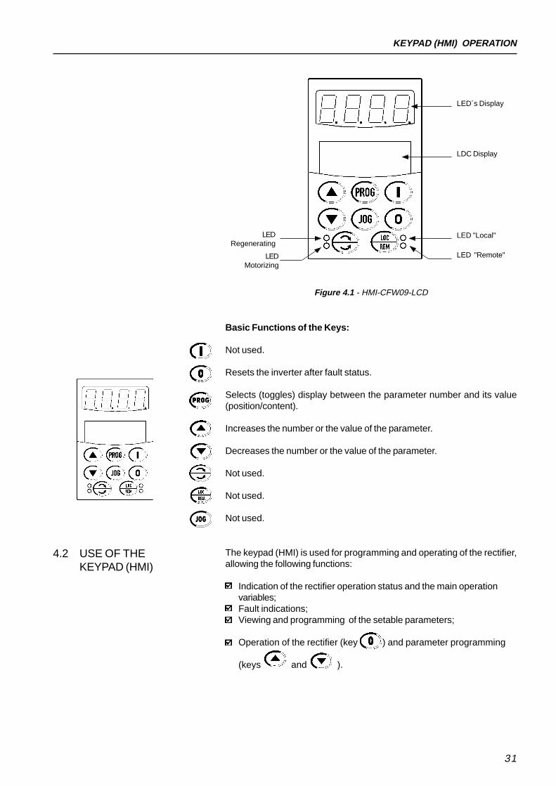
4.1 DESCRIPTIONOF THE KEYPADHMI-CFW09-LCD
The standard CFW-09RB Keypad has a 4 digit, seven-segment displayand an LCD display with two lines of 16 alphanumeric characters.There are also 4 indicator LED’s and 8 keys.Figure 4.1 shows the front view of the Keypad and indicates the positionof the displays and status LED’s.
Functions of the LED Display:The LED Display shows the fault codes and status (see QuickParameter Reference, Fault and Status Messages. The LED displayat the right side indicates the unit of the variable:
: A current (Amps). U voltage (Volts)· H frequency (Hertz)· Blank speed and other parameters
When the value is equal to or higher than 1000 (Amps or Volts), thevariable unit will not be shown (ex.: 568.U, 999.A, 1000., 1023., etc.)
Functions of the LCD Display:The LCD Display shows the parameter number and its valuesimultaneously,without requiring the toggling of the key. It also provides a briefdescription of each parameter function, indicating the respective units(A, Hz, V, s, %, etc.). It also provide a brief description of the rectifiererror or status.
LOCAL and REMOTE LED’s
Rectifier always in Local Mode:Green LED ON and Red LED OFF.
Direction of Rotation (FWD / REV) LED’s:It indicates if the rectifier is motorizing (red LED ON)or regenerating (green LED ON). See Fig. 4.1.
KEYPAD (HMI) OPERATION
31
Figure 4.1 - HMI-CFW09-LCD
LED "Remote"
LED "Local"
LDC Display
LED´s Display
LEDRegenerating
LEDMotorizing
Basic Functions of the Keys:
Not used.
Resets the inverter after fault status.
Selects (toggles) display between the parameter number and its value(position/content).
Increases the number or the value of the parameter.
Decreases the number or the value of the parameter.
Not used.
Not used.
Not used.
The keypad (HMI) is used for programming and operating of the rectifier,allowing the following functions:
Indication of the rectifier operation status and the main operationvariables;Fault indications;Viewing and programming of the setable parameters;
Operation of the rectifier (key ) and parameter programming
(keys and ).
4.2 USE OF THEKEYPAD (HMI)

KEYPAD (HMI) OPERATION
32
All functions relating to the rectifier operation can be executed throughthe HMI.
Description of the Keypad Keys for the Rectifier Operation:All functions relating to the rectifier operation can be executed throughthe HMI.
These functions can also be executed jointly or individually by meansof digital and analog inputs. Thus programm the parameter related tothese functions and to these corresponding inputs.Please find below description of the HMI Keypad keys used for therectifier operation:
Not used.
Not used.
“0”: It resets the reCtifier after a fault trip (Always active).
Not used.
Not used.
When pressed, it increases the parameter number or its content.
When pressed, it decreases the parameter number or its content.
4.2.1 Use of the Keypad (HMI)
4.2.2 Signallings/Indications on the HMIDisplays
P205 Initial Monitoring Parameter
0 P002 (Line voltage)1 P003 (Input current)2 P004 (DC voltage)3 P006 (Rectifier voltage)4 P010 (Input power)5 P042 (hours energized)6 P043 (hours enabled)
a) Monitoring variables:
The monitoring variable to be shown after AC power is applied to therectifier is defined in Parameter P205:
Rectifier Ready
Rect. Status
P006=run
b) Rectifier status:
Inverter is READY to be started
Inverter is enabled (‘Run’)

KEYPAD (HMI) OPERATION
33
Undervoltage
DC link
Line voltage is too low for inverter operation(Undervoltage condition)
c) LED display flashes:The display flashes in the following conditions:
trying to change a parameter value when this is not permitted.rectifier in overload condition (refer to chapter - Maintenance)Rectifier in Fault condition (refer to chapter - Maintenance)
All RECTIFIER settings are made through the parameters. The parametersare shown on the display with the letter P followed by a number:Example (P151):
151 = Parameter number
Each parameter is associated to a numerical value (parameter content).
The parameter values define the rectifier programmationor the variable value(ex.: current, frequency, voltage).For rectifier programming, parameter (s) content(s) must be changed.
DC Voltage level
P151=618 V
4.3 PARAMETERPROGRAMMING
ACTION DISPLAY HMI LED CommentsDISPLAY HMI LCD
DC Voltage Level
P151=618 V
DC Link Voltage
P004=504 V
Press the key
Use the keys and
Press the key
Selects the desired parameter
Numeric value associated to theparameter
DC Voltage Level
P151=618 V
4.3.1 Parameter Selection/Programmin:

KEYPAD (HMI) OPERATION
34
*1 - For parameters that can be changed with enabled rectifier, therectifier will use the new value immediately after it has been set. Forthe parameters that can be changed only with rectifier disabled, therectifier will use this new set value only after the key ispressed.
*2 - By pressing the key after the reprogramming, the last setvalue will be stored automatically in the non-volatile memory until anew value is programmed.
*3 - To allow the reprogramming of any parameter value it is requiredto change parameter P000 to the password value. The factory defaultpassword value is 5. Otherwise you can only read the parameter valuesand not reprogram them.For more details see P000 description in Chapter 5.
ACTION DISPLAY HMI LED CommentsDISPLAY HMI LCD
Use the keys and
Press the key
Sets the new desired value *1
*1, *2, *3
DC Voltage Level
P151=615 V
DC Voltage Level
P151=615 V

35
CHAPTER 5
DETAILED PARAMETER DESCRIPTION
This Chapter describes in detail all rectifier parameters. In order to simplifythe explanation, the parameters have been grouped by characteristicsand functions:
Symbols and definitions used in the text below:
‘(1)' indicates that the parameter can be changed only with the rectifierdisabled.
Read Only Parameters Variables that can only be viewed on thedisplay but can not be not changed bythe user.
Regulation Parameters Programmable values to be used bythe rectifier functions.
Configuration Parameters They define the rectifier characteristics,the functions to be executed, as well asthe input/output functions of the controlboard.
5.1 ACCESS AND READ ONLY PARAMETERS - P000....P099
This parameter releases the access to change the parameter content. With the factory default password is [P200= 1 (Password active)] you must set P000=5 to change the parameter contents, i. e., the
password value is equal to 5.
P000 0...999Access Parameter/ [0]Password value -Setting
Range[Factory Setting]
Parameter Unit Description/Notes
P002 0 ... 600Line Voltage [ - ]
1V
P003 0...2600 AInpiut Current [ - ]
0,1A (<100)-1A (>99,9)
P004 0...1077DC Link Voltage [ - ]
1V
P006 Rdy, run, sub, ExyRectifier Status
Indicates the input line voltage in Volts
Indicates the rectifier input current in Amps.
Indicates the DC Link voltage in Volts.
Indicates the rectifier status:'rdy' rectifier is ready to be started or enabled;'run' rectifier is enabled;'Sub' rectifier is disabled and line voltage is too low for operation(undervoltage). It doe not receive enabling controls;'Exy' inverter is in a fault condition, ‘xy’ is the number of the Fault code
P010 0.0...1200 kWInput Power [ - ]
0,1kW
Indicates the instantaneous input power in kW.

DETAILED PARAMETER DESCRIPTION
36
Indicates on the Keypad LCD display the status of the 2 digital inputsof the control board (DI1 to DI2). Letter A stands for Active and letter Istands for Inactive in the following order:
DI2, DI1The LED display of the HMI Keypad shows a decimal value related to the2 Digital Inputs, where the status of each input is considered one bit in thespecified sequence: Active = 1, Inactive = 0 and the DI2 status is the mostsignificant bit (MSB).Example:DI2=Active (+24V); DI1=Inactive (0V)This is equivalent to the bit sequence:
10which correponds to the decimal number 2.Thus the keypad displays will be as follows:
Range[Factory Setting]
Parameter Unit Description/Notes
P012 LCD= A, IStatus DI1...DI2 LED= 0 ... 255
[ - ]-
Status DI2...DI1P012= AI
P013 LCD = A, IDigital and Relay LED = 0...255Outputs DO1, DO2 [ - ]RL1, RL2 and RL3 -Status
Indicates on the Keypad LCD Display the status of the 2 Digital Outputsof the I/O Expansion Board (D01, D02) and the 3 Relay Outputs of thecontrol board. Letter A stands for Active and letter I stands for Inactive,in the following order:D01, D02, RL1, RL2, RL3.The LED display shows a decimal value related to the status of the 5Digital Outputs, where the status of each output is considered one bitof a binary number where Active = 1, Inactive = 0 and the status ofDO1 is the most significant bit (MSB). The 3 least significant bits arealways ‘0’.Example:DO1=Inactive; DO2=InactiveRL1=Active: RL2=Inactive; RL3=activeThis is equivalent to the binary sequence:
00101000Which corresponds to the decimal number 40.The Keypad displays will be:
Status DO1...RL3P013= IIAIA
P014 E00...E41Last Fault [ - ]
-P015 E00...E41Second Previous Fault [ - ]
-P016 E00...E41Third Previous Fault [ - ]
-P017 E00...E41Fourth Previous Fault [ - ]
-
Indicate the code of the last, second, third and fourth previous Faults.Fault Sequence: Systematic recordExy → P014 → P015 → P016 → P017

DETAILED PARAMETER DESCRIPTION
37
Range[Factory Setting]
Parameter Unit Description/Notes
P022 -WEG Use [ - ]
-P023 X.XXSoftware Version [ - ]
-
P024 LCD: -32768...32767A/D Conversion LED: 0...FFFFHValue of the Analog [ - ]Input AI4 -
P025 0...1023A/D Conversion [ - ]Value of Iv Current -
P026 0...1023A/D Conversion [ - ]Value of Iw Current -
P027 -WEG Use [ - ]
-P028 -WEG Use [ - ]
-P029 -WEG Use [ - ]
-
Indicates the Software version stored in the microcontroller memoryconfigured on the control board.
ndicates the A/D conversion result of the analog input A14 located onthe I/O Expansion Board.The LCD display indicates the conversion value as a decimal numberand the LED display as a hexadecimal number with negative valuesin supplement of 2.
P025 and P026 indicate the A/D conversion result, in module, of theV and W phase currents, respectively.
Indicates the total number of hours that the rectifier was powered. The LED Display shows the total number of hours that the rectifier was energized divided by 10. This value remains stored even when the rectifier is turned OFF. Example: Indication of 22 hours powered.
Indicates the total number of hours that the rectifier was enabled. Indicates up to 6553 hours, rolls over to 0000. If P204=3 is set to 3, the Parameter P043 is reset to zero. This value remains stored even when the rectifier is turned OFF.
P042 LCD: 0...65530hTime Powered LED: 0...6553h (x10)
[ - ]-
P043 0...6553hTime Enabled [ - ]
-
Hours EnergizedP042 = 22 h
P121 -100%...100%Reactive Current [0.0]Reference 1%
The value of P121 is the reactive current reference. If negative, theinput current will be advanced relating to the voltage (capacitive). Ifpositive, the input current will be delayed relating to the voltage(inductive).
If maintained at zero, the current will be in phase with the voltage.The standard factory setiing is P121=0. This setting ensures a powerfactor near to zero at the rectifier input.Do not change this value before contacting WEG Automação.

DETAILED PARAMETER DESCRIPTION
38
Range[Factory Setting]
Parameter Unit Description/Notes
5.2 REGULATION PARAMETERS - P100 ....P199
P151 322V... 394V (P296=0)DC Volatge Level [358V]
1V
556V...680V (P296=1)[618V]
1V
585V...715V (P296=2)[650V]
1V
646V...790V (P296=3)[718V]
1V
675V...825V (P296=4)[750V]
1V
The standard value of this parameters changes with P296.
Figure 5.1 - Block Diagram of the DC Link Voltage
P156 0- ... 1.3xP295Overload [1.1x 295]Current 0,1A(<100) - 1A(>99.9)
Figure 5.2 - Ixt Function - Overload detection
Used for protection against overload (Ixt - E05).The Overload Current (P156, P157 and P158) is the current level abovewhich the rectifier will consider the inductor operating under overload.The higher the difference between the inductor currente and the overloadcurrent, the sooner the Overload Fault E05 will occur.The Parameter P156 (overload current) must be set 10% higher thanthe used rated rectifier current (P295).
P161 0.0...63.9Proportional [5.0]DC Gain -
The standard values of the gains of P161 and P162 meet the mostcases and do not require any setting.By increasing the P161 gain, we will have a faster DC Link regulationwith less increase.
P151
Link CC
P161, P162
Time (seg.)
Motor Current (P003)Overload Current

DETAILED PARAMETER DESCRIPTION
39
Range[Factory Setting]
Parameter Unit Description/Notes
P162 0.000...9.999DC Proportional [0.009]Gain -
By increasing the P162 gain, we will have a better DC Link regulationwith faster response, increasing the overshoot during enabling, whichmay cause overcurrent in this condition.Figure 5.3a shows the effect by increasing P162, thus changing theDC Link voltage level during enabling. According to P162, the voltageincrease tends to exceed the rated value, thus causing an overcurrent.Figure 5.3b shows the effect of the proportional gain by changing theDC Link voltage level during enabling. The increase of the proportionalgain causes a faster response time. A too high proportional gain cancause an overcurrent.Figure 5.3c shows what happens with the DC Link voltage, when theload increases suddenly, and the proportional gain changes.Increasing the proportional gain, will has a faster response and lessundershoot voltage. A too low gain may cause undervoltage in theDC link circuit.Figure 5.3d shows the effect on the DC link voltage when a load isapplied on the rectifier and the integral gain is varied. By increasingthe integral gain will cause a faster recover of the DC link voltage.A higher P162 Parameter will decrease the error between the DClink voltage and the reference (P151).It is recommended to vary the gains proportionally. Thus when P161is increased also increase P162 proportionally. The same proceduresshould be adopted when the gains are reduced.
Figure 5.3 - Effect of the Gain Change
a b
c d
660
640
620
600
580
560
540
5200 0.1 0.2 0.3 0.4 0.5 0.6 0.7
P162 increases
0 0.1 0.2 0.3 0.4 0.5 0.6 0.7
630620610600590580570560550540530
P161 Increases
0 0.5 1 1.5 2
620
610
600
590
580
570
560
P161 IncreasesP162 Increases
0 0.5 1 1.5 2
620
610
600
590
580
570
560
DC Link (V)
Time (s)
DC Link (V)
DC Link (V) DC Link (V)
Time (s)
Time (s) Time (s)

DETAILED PARAMETER DESCRIPTION
40
Range[Factory Setting]
Parameter Unit Description/Notes
P167 0.00... 1.99Current Regulator [0.7]Proportional Gain -
P168 0.000... 1.999Current Regulator [0.250]Integral Gain -
The gains of P167 and P168 are already set. User shall maintain thestandard values.If the standrad inductance is used that is supplied with the product,please change these gains.
P169 0 ... 150%Max. Braking [100%]Current 1%
It limits the maximum line current in the braking condition (energy isreturned to the line)In this coindition the current has a 180º offset relating the inputcurrent.
P170 0 ... 150%Max. Motorizing [100%]Current 1%
It limits the maximum line current in the motorizing condition (lineenergy absorption).The motorizing current is the current that flows from the line to theDC Link.In this condition the current will be in phase with the input voltage.
P175 0.0...31.9Proportional Gain [3.3]of the Reactive -Regulator
P176 0.000... 9.999Integral Gain [0.067]of the Reactive -Regulator
The gains of P175 and P176 are already set. User shall maintain thestandard values.
P179 0...120%Maximum Reactive [120%]
1%
P180 0...120%Point of [120%]Reative Generation 1%
Parameters P179 and P180 are associated to the reactive generationby the rectifier. When the line voltage exceeds percentually the valueset at P180 (the rated voltage of the rectifier corresponds to 100%),the rectifier starts to inject reactives. The reactive injection ensuresthat the DC Link voltage remains at the value set at P151.The reactive injection is the offset of the input current relating to thevoltage and the current will be delayed by 90º (inductive).These parameters are useful for minimizing the line transient effectsthat could cause overvoltages.The voltage "excess" is transferred to the input reactance.
5.3 CONFIGUREATION PARAMETERS - P200 ....P399
P200 Result0 (Off) It permits to change the parameters
content independentlyof P000
It permits only to change the1 (On) parameters content
when P000 is equal to the valueof the password.
P200 0...1Password [ 1 ](activates/deactivates -the password)
With factory setting, the password is P000=5.To change the password, see P000.

DETAILED PARAMETER DESCRIPTION
41
Range[Factory Setting]
Parameter Unit Description/NotesP201 0...2Language Selection [ to be defined
by the user ]-
0=Portuguese1=English2=Spanish
CurrentInverter
Parameters
FactoryDefault(WEG
standard)
P204 0...11Loads / Saves [ 0 ]Parameters -(1)
Figure 5.4 – Parameter Transfer
The parameters P295 (Rated Current) and P296 (Rated Voltage),P297 (Switching Frequency) are not changed when the factory defaultparameters are loaded through P204 = 5.
NOTE!The parameter load/save action will be effected only
after the parameters have been set and key is pressed.
P204Action0, 1, 2, 4, Sot Used:
6, 9 No action3 Reset P043: Resets the Time
Enabled hour meter to zero.5 Load WEG:
Resets all parameters to the factorydefault values.
P205 0...6Selection of the [ 2 ]indicated Read -Parameter
Selects which of the read parameters listed below will be shown onthe display, after the rectifier is powered up:0=P002 (line Voltage)1=P003 (Input Current)2=P004 (DC Link Voltage)3=P006 (Rectifier Status)4=P010 (Input Power)5=P042 (Time ON)6=P043 (Time enabled)
P206 0...255Auto-Reset [ 0 ]Time 1s
≥
In the event of a fault trip, except when E09, E31 or E41, therectifier can initiate an automatic reset after the time given by P206is elapsed.If P206 2 Auto-Reset does not occur.If after Auto-Reset the same fault is repeated three times consecutively,the Auto-Reset function will be disabled. A fault is consideredconsecutive if it happens again within 30 seconds after Auto-Reset.Thus if a fault occurs four times consecutive, this fault will bedisplayed permanently (and the rectifier will be disabled).
P218 0 ... 150LCD Display [127]Contrast Adjustment
This parameter is useful only for rectifiers provided with a keypad(HMI) with LCD display.It allows the adjustment of the LCD Display contrast to obtain abetter visualization.

DETAILED PARAMETER DESCRIPTION
42
P251 0 ... 3A01 Output Function [0]
-
Check in Table 5.1 all possible options.
Range[Factory Setting]
Parameter Unit Description/Notes
P252 0.000 ... 9.999A01 Output Gian [1.000]
0.001P253 0 ... 3A02 Output Function [0]
-
Check in Table 5.1 all possible options.
P254 0.000 ... 9.999A02 Output Gain [1.000]
0.001
P255 0 ... 25A03 Ouput Function [0](located on the -optional EBA board)
Check in Table 5.1 all possible options.For more information about the AO3 output, check items8.1.1 and 8.1.3 of the CFW-09 Frequency Inverter Manual.
P256 0.000 ... 9.999A03 Output Gain [1.000]
0.001
P257 0 ... 25A04 Ouput Function [0](located on the -optional EBA board)
Check in Table 5.1 all possible options.For more information about the AO3 output, check items8.1.1 and 8.1.3 of the CFW-09 Frequency Inverter Manual.
P258 0.000 ... 9.999A04 Output Gain [1.000]
0.001
Table 5.1 - Functions of the Analog Outputs
P251 0 1 2 3 -(AO1) P253 0 1 2 3 -(AO2) P255 0 1 2 3 4...25(AO3) P257 0 1 2 3 4...25(AO4)
Line
Vol
tage
Inpu
t Cur
rent
DC
Lin
Vol
tage
Inpu
t Pow
er
Excl
usiv
e us
e of
W
EG

DETAILED PARAMETER DESCRIPTION
43
Range[Factory Setting]
Parameter Unit Description/Notes
P263 2...2DI1 Digital Input [ 2 (Gen. enabling) ]Function -
P264 4...4DI2 Digital INput [ 4Function (without ext. fault) ]
-
The status of the digital inputs can be monitored at parameter P012.
P251P253P255P257
Gain AOX
P252, P254, P256, P258
Input Power
DC Link Voltage
Input Current
Line Voltage
Scale of the Analog Outputs indications:- Full scale = 10V:Line Voltage: full scale = 1,4 x P296Input Current: full scale = 1,6 x P295DC Link Voltage: full scale = 2 x P296Input Power: full scale = 2,04 x 3 φ P295 x P296
Figure 5.5 - Block diagram of the Analog Outputs
Time
Time
WITHOUT EXTERNAL FAULT
Regulatorsenabled
Regulatorsdisabled
24 V
DI - without ext. fault open
GENERAL ENABLING
Regulatorsenabled
Regulatorsdisabled
24 V Time
Time
DI open
Figure 5.6 - Details about the operation of the Digital Inputs Functions
DETAILED PARAMETER DESCRIPTION
44
Range[Factory Setting]
Parameter Unit Description/Notes
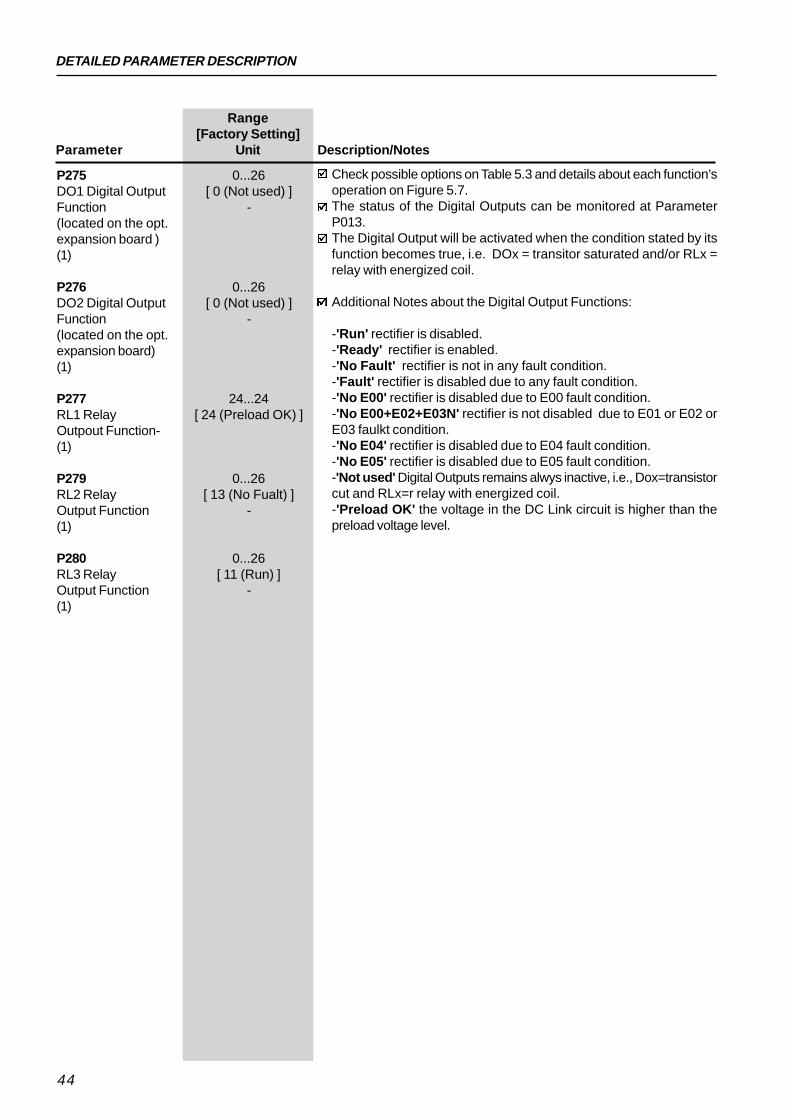
P275 0...26DO1 Digital Output [ 0 (Not used) ]Function -(located on the opt.expansion board )(1)
P276 0...26DO2 Digital Output [ 0 (Not used) ]Function -(located on the opt.expansion board)(1)
P277 24...24RL1 Relay [ 24 (Preload OK) ]Outpout Function-(1)
P279 0...26RL2 Relay [ 13 (No Fualt) ]Output Function -(1)
P280 0...26RL3 Relay [ 11 (Run) ]Output Function -(1)
Check possible options on Table 5.3 and details about each function’soperation on Figure 5.7.The status of the Digital Outputs can be monitored at ParameterP013.The Digital Output will be activated when the condition stated by itsfunction becomes true, i.e. DOx = transitor saturated and/or RLx =relay with energized coil.
Additional Notes about the Digital Output Functions:
-'Run' rectifier is disabled.-'Ready' rectifier is enabled.-'No Fault' rectifier is not in any fault condition.-'Fault' rectifier is disabled due to any fault condition.-'No E00' rectifier is disabled due to E00 fault condition.-'No E00+E02+E03N' rectifier is not disabled due to E01 or E02 orE03 faulkt condition.-'No E04' rectifier is disabled due to E04 fault condition.-'No E05' rectifier is disabled due to E05 fault condition.-'Not used' Digital Outputs remains alwys inactive, i.e., Dox=transistorcut and RLx=r relay with energized coil.-'Preload OK' the voltage in the DC Link circuit is higher than thepreload voltage level.

DETAILED PARAMETER DESCRIPTION
45
Range[Factory Setting]
Parameter Unit Description/Notes
Parameter P275 P276 P277 P279 P280 Function (DO1) (DO2) (RL1) (RL2) (RL3)
Not used 0 0 24 0 0Not used 1 1 24 1 1Not used 2 2 24 2 2Not used 3 3 24 3 3Not used 4 4 24 4 4Not used 5 5 24 5 5Not used 6 6 24 6 6Not used 7 7 24 7 7Not used 8 8 24 8 8Not used 9 9 24 9 9Not used 10 10 24 10 10
run 11 11 24 11 11ready 12 12 24 12 12
No Fault 13 13 24 13 13No E00 14 14 24 14 14
No E01+E02+E03 15 15 24 15 15No E04 16 16 24 16 16No E05 17 17 24 17 17
Not used 18 18 24 18 18Not used 19 19 24 19 19Not used 20 20 24 20 20Not used 21 21 24 21 21Not used 22 22 24 22 22Not used 23 23 24 23 23
Preload OK 24 24 24 24 24No Fault 25 25 24 25 25Not used 26 26 24 26 26
Table 5.3 - Functions of the Digital Outputs
Relay /Transistor
ON ONOFF
Time
PreloadLevel
Preload OK
Relay /TransistorON
No EOX
OFF
Time
with EOX
DC Link
Figure 5.7 - Details about the operartion of the Digital Output Functions
P295 17 ... 25Rectifier rated [According tocurrent Rectifier rated(1) current]
-
17=86.0A; 18=105.0A; 19=130.0A; 20=142.0A; 21=180.0A;21=205.0A; 22=240.0A; 23=300.0A; 24=350.0A; 23=361.0A;26=400.0A; 24=450.0A; 28=580.0A; 25=600.0A; 26=400.0A;24=450.0A; 28=580.0A; 25=600.0A; 26=650.0A; 27=810.0A;28=1080.0A; 29=1215.0A; 30=1620.0A.

DETAILED PARAMETER DESCRIPTION
46
Range[Factory Setting]
Parameter Unit Description/Notes
P296 0...4Rated Voltage [According to(1) Rectifier
Supply Voltage]-
0=220V/230V1=380V2=400V/415V3=440V/460V4=480VFor rectifiers with rated current ( 86A and rated voltage from 380V to480V, adjust also the voltage selection jumper (Refer to the CFW-09 Inverter Manual).
P297 1...2Switching [ 2 (5.0 kHz) ]Frequency -(1)
1=2.5 kHz2=5.0 kHzFor the models 180 ... 600S, used the switching frequency of2.5kHz.The switching frequency is a compromise between the motor acousticnoise level and the inverter IGBTs losses. Higher switching frequenciescause lower motor acoustic noise level, but increase theIGBTs losses, increasing drive components temperature, thusreducing their useful life.The predominant frequency on the motor is twice the switchingfrequency programmed at P297.P297 = 5.0 kHz results in an audible motor noise corresponding to10.0 kHz. This is due to the PWM technique used.A reduction of the switching frequency also:- Helps reducing instability and resonance problems that may occurin certain application conditions.- Reduces the leakage currents to ground, which may avoid nuisanceof E11 (short-circuit between phase-earth at the output).

47
CHAPTER 6
DIAGNOSTICS AND TROUBLESHOOTING
This Chapter assists the user to identify and correct possible faultsthat can occur during the operation. Guidance on PreventiveMaintenance is also provided.
When a fault is detected, the inverter is disabled and the Fault Code isdisplayed on the readout in the EXX form, where XX is the actual FaultCode.To restart the inverter after a fault has occurred, the inverter must bereset. The reset can be made as follows:
disconnecting and reapplying AC power (power-on reset);by pressing the key “0/RESET” (manual reset)automatic reset through P206 (auto-reset);
The table below defines each Fault Code, explains how to reset thefault and shows the possible causes for each Fault Code.
6.1 FAULTS AND POSSIBLECAUSES
FAULT RESET POSSIBLE CAUSES
E00 Power-on Short-circuit between two input phases;Input Manual (Key 0/RESET) Inertia of the load is too high, or acceleration ramp is too
Overcurrent Autoreset short;Transistor module is shorted;Input reactance is not present;Regulation and/or configuration parameter(s) are incorrect.P169, P170, P161, P162 set too high;Wrong synchronism connections.
E01 Power supply voltage too high, generating in the DC LinkDC Link a voltage higher than permitted
Overvoltage Ud>400V - Models 220-230V(Ud) Ud>800V - Models 380- 480V
Inertia of the load is too high, or acceleration ramp is toohigh, or acceleration ramp is too shortP169 or P179 set too low.
E02 Power supply voltage too low, generating in the DC LinkDC Link a voltage lower than permitted
Undervolatge (read value at Parameter P004):(Ud) Ud < 223V - Models 220 - 230V
Ud < 385V - Models 380VUd < 405V - Models 400 - 415VUd < 446V - Models 440 - 460VUd < 487V - Models 480VPhase loss at the input;P169 set too low;Pre-charge contactor defective;Parameter P296 set to a voltage higher than the rated livevoltage.

DIAGNOSTICS AND TROUBLESHOOTING
48
FAULT RESET POSSIBLE CAUSES
E03 Power Supply voltage is too lowInput Undervoltage/ UaIim < 154V for models 220-230VPhase Loss (1) UaIim < 266V for models 380-480V
Phase loss at the inverter input.Activation time: 2,0 seg
E04 Ambient temperature too high (>40°C) and/or output Inverter current too high; or ambient temperature <-10°C
Overtemperature Blowers locked or defective (3) or Pre-charge Pre-charge circuit fuse blown (see Section 3.2.3);
Circuit The supply voltage is lower the min.a permittedDefective (2) (3) value or phase loss, if they occur during more than 2
seconds and without phase loss detection.P214= 0(disable).
E05 Power-on P156 set too high for the Inout Manual (tecla 0/RESET) used motor;
Overload, IxT Autoreset Load at motor shaft too highfunction(see P156)
E06 Wiring at DI1...DI2 inputs is open (not connected to a External fault + 24V):(opening at dig. XC12 coonector on the CC( control board is not connected) inout programmedto withoutpara fault)
E08 Electrical noise. CPU Error
(watchdog)
E09 Contact WEG Memory with corrupted values. Program Memory (refer to Item 6.3)
Error
E16 Power-on Line Voltage oscillation higher than the permiteed one.Line Manual (key 0/RESET)
Overvoltage Autoreset
E31 It is automatically reset when Keypad (HMI) cable with bad contact Keypad (HMI) HMI communication with Electrical noise in the installation (eletromagneticconnection fault inverter is restablished interferecen)
E41 Contact WEG Memory error or any internal inverter circuit defective.Self-Diagnois refer to Item 6.3)
Fault
Note:2) In case of E04 Fault due to inverter overtemperature, allow the in
verter to cool before trying to reset it.The failure in the pre-charge circuit means that the pre-chargecontactor (sizes up to 142A) or pre-charge thyristor (sizes above142A) is not closed, thus overheating the pre-charge resistors.
(3) For 220-230V Models with rated current equal or higher than 105 Aor 380-480V Models with rated current equal or higher than 86A,and equal or lower than 142A, E04 Fault can also be caused byinternal airflow overtemperature. In this case, check the blower ofthe electronics.
DIAGNOSTICS AND TROUBLESHOOTING
49
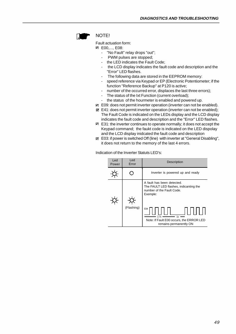
NOTE!Fault actuation form:
E00,..., E08:- "No Fault" relay drops "out";- PWM pulses are stopped;- the LED indicates the Fault Code;- the LCD display indicates the fault code and description and the
"Error" LED flashes.- The following data are stored in the EEPROM memory:- speed reference via Keypad or EP (Electronic Potentiometer; if the
function "Reference Backup" at P120 is active;- number of the occurred error, displaces the last three errors);- The status of the Ixt Function (current overload);- the status of the hourmeter is enabled and powered up.E09: does not permit inverter operation (inverter can not be enabled).E41: does not permit inverter operation (inverter can not be enabled);The Fault Code is indicated on the LEDs display and the LCD displayindicates the fault code and description and the "Error" LED flashes.E31: the inverter continues to operate normally; it does not accept theKeypad command; the faukt code is indicated on the LED dispolayand the LCD display inidcated the fault code and descriptionE03: if power is switched Off (line) with inverter at "General Disabling",it does not return to the memory of the last 4 errors.
Indication of the Inverter Statuts LED's:
Description
Inverter is powered up and ready
(Flashing) E04
2,7s 1s
A fault has been detected.The FAULT LED flashes, indicanting thenumber of the Fault Code.Exemple:
Note: If Fault E00 occurs, the ERROR LEDremains permanently ON
LedError
LedPower

50
CHAPTER 7
TECHNICAL SPECIFICATIONS
This Chapter describes the technical specifications (electrical andmechanical) of the CFW-09RB inverter series.
AC Input Specifications:Voltage : + 10%, -15%;Frequency : 50/60Hz (± 2 Hz);Phase Unbalance 3%;Overvoltage Category III (EN 61010/UL 508C);Transient voltages according to Category III;
Power-up: 10 ON/OFF cycles per hour maximum.
≥
7.1 POWER DATA
7.1.1 220-230V Power Supply
Note: CT = Constant Torque VT = Variable Torque
Factory Default
7.1.2 380-480V Power Supply
Note: CT = Constant Torque VT = Variable Torque
Factory Default
Model: Current / voltage
Load (1)
Power (kVA) (2)
Rated Input Current (A) (3)
Maximum Input Current (A) (4)
Switching Frequency (kHz)DC Rated Current (A)Rated Dissipated Power (kW)Frame Size
105/220-230CT VT40 50
105 130158
5 2.5121 1501.2 1.5
6
130/220-230CT VT50 62
130 163195
5 2.5150 1871.5 1.7
6
180/220-230CT/VT
691802702.5207
38
240/220-230CT/VT
912403602.5276
48
361/220-230CT/VT1383615422.5415
69
450/220-230CT/VT1714506752.55187.610
600/220-230CT/VT2296009002.56901010
Model: Current / Voltage
Load (1)
Power (kVA) (2)
Rated Input Current (A) (3)
Maximum Input Current (A) (4)
Switching Frequency (kHz)Rated DC Current (A)Rated Disspated Power (kW)Frame Size
86/380-480CT VT66 8286 108
1295 2.5
99 1241.2 1.5
6
105/380-480CT VT80 99
105 130158
5 2.5121 1501.5 1.7
6
180/380-480CT/VT1371802702.5207
38
240/380-480CT/VT1832403602.5276
48
361/380-480CT/VT2753615422.5415
69
450/380-480CT/VT3434506752.55187.610
600/380-480CT/VT4576009002.56901010
142/380-480CT VT108 136142 178
2135 2.5
163 2052.4 2.9
7

TECHNICAL SPECIFICATION
51
(2)The power rating in kVA is determined by the following equation:
P(kVA) = 3. Voltage(V). Current (Amp.)1000
The values shown on the Table were calculated, considering the inverterrated current rating and an input voltage of 230V for 220-230V models and460V for 380-480V models
(3)Rated Output Current in the following conditions:
Relative Air Humidity: 5 to 90%, non condensing;Altitude : 3300 ft (1000m), up to 13200 ft (4000m) with 10% derating /3300 ft (1000 m);Ambient Temperature: 32º to 104ºF (0º to 40º C), up to 122ºF (50º C)with 2% / ºC derating;
(4)Maximum Current: 1.5 x I Nominal (for 60 seconds every 10 minutes).I Nominal = Rated Current for CT applications;The maximum output current is the same for CT and VT. That means alower overload capacity in VT for the models with a higher rated currentfor VT than for CT.
NOTES:(1)
Torque Torque
Nnom
Speed Speed
Nnom
Tn Tn
CT -Constant Torque VT - Variable Torque
Figure 7.1 - Load Characteristics

52
APPENDIX A
Figure A.1- CFW-09...RB Capacitive Filter
Figure A.2 - Kit KRB
Figure A.1 shows the configuration of the CFW-09...RB CapacitiveFilter.
This capacitive Filter is supplied by WEG Automação in two differentconfigurations for meeting the servodrive power:- Module KMR1: for servodrives with current lower than 180A (WEG
Item No. 417102043)- Module KMR2: for servodrives with current equal to or higher than
180A (WEG Item No. 417102042)Figure A.2 shows the KMR Filter Module.
The KMR1 module has a capacitor series connected between theinput phases, whereas the KMR2 module is fitted with two capacitorsparallel connected between the input phases.The used capacitor is made of polypropylene film and has a capacitanceof 0.56mF/1200V (ICEL-PMB2123560KSP, item WEG: 0302.4793).

53
APPENDIX B
The CFW-09RB input reactance has special characteristics. Thusdon´t use a standard line reactance. Table XX shows the modelsand WEG Item Numbers for these reactances.
Voltage
220 V
230 V
380 V
400 V
440 V
480 V
Model10513018024036145060010513018024036145060086
10514218024036145060086
10514218024036145060086
10514218024036145060086
105142180240361450600
Item WEG of Reactance0299.00470299.00480299.00490299.00500299.01250299.01270299.01290299.00510299.00520299.00530299.00540299.01260299.01280299.01300299.00550299.00560299.00570299.00580299.00590299.00600299.00610299.00620299.00630299.00640299.00650299.00660299.00670299.00680299.00690299.00700299.00710299.00720299.00730299.00740299.00750299.00760299.00770299.00780299.00870299.00880299.00890299.00900299.00910299.00920299.00930299.0094
For 460 V voltage use the 480 V reactance of the same model.
For voltages not indicated in this table, contact WEG Automação.