serial rapidio physical layer interface ip user’s guide · serial rapidio physical layer...
TRANSCRIPT

ispLeverCORECORE
TM
October 2005ipug26_02.0
Serial RapidIO Physical Layer Interface
User’s Guide

2
Serial RapidIO Physical Layer InterfaceLattice Semiconductor User’s Guide
Introduction
RapidIO is a high performance, low pin count, packet switched, full duplex, system level interconnect architecture.The architecture addresses the need for faster bus speeds in an intra-system interconnect for microprocessors,digital signal processors, communications and network processors. It also offers error management and provides awell-defined architecture for recovering from and reporting transmission errors.
RapidIO systems contain endpoint and switch processing elements. The RapidIO interconnect architecture is parti-tioned into a layered hierarchy of specifications which includes Logical, Common Transport and Physical layers.The Logical layer defines the operations and transactions by which endpoint processing elements communicatewith each other. The Common Transport layer defines how the transactions are routed from one endpoint process-ing elements to another through switch processing elements. The Physical layer defines the interface between twodevices and the packet transport mechanism, flow control and electrical characteristics. Currently there are twodefined Physical layer specification, an 8-bit or 16-bit wide parallel specification and a 1-lane (1x) or 4-lane (4x)serial specification.
This user’s guide explains the information about Lattice’s Serial RapidIO Physical Layer specification and interface.
The Serial RapidIO Physical Layer core comes with the following documentation and files:
• Data sheet
• User’s guide
• Lattice evaluation gate level netlist
• Simulation model for evaluation
• Core instantiation template
• Testbench and testbench coding template
The following experience is recommended for the user to implement a design using this IP:
• Familiarity with the Lattice ORCA
®
ORT82G5/ORT42G5 FPSC architecture
• Familiarity with simulation, synthesis and Lattice ispLEVER
®
design tools
• Knowledge of the
RapidIO Interconnect Specification Part VI: Physical Layer 1x/4x LP-Serial Specification Rev. 1.2,
06/2002
Features
• Supports high speed 1x mode (up to 2.5 Gbps)
• 8B/10B encoding and decoding
• Clock and Data Recovery (CDR)
• Lane synchronization
• CRC generation and checking
• Error detection
• Packet/control symbol assembly and de-assembly
• Simple user interface for easy integration into user logic
• Targets ORT82G5/ORT42G5 FPSC

3
Serial RapidIO Physical Layer InterfaceLattice Semiconductor User’s Guide
General Description
The Serial RapidIO core supports the physical layer specification as defined in the
RapidIO Specification Rev 1.2.
The Serial RapidIO Physical Layer defines a protocol for packet delivery between Serial RapidIO devices and otherdevices, including packet transmission, flow control, error management and link maintenance protocols. The coresupports one-lane high speed (1x mode) running at 1.0, 2.0 Gbps or a maximum of 2.5 Gbps.
This Serial RapidIO core is optimized to support ORT82G5/ORT42G5 FPSCs.
For more information on Lattice products, refer to the Lattice web site at www.latticesemi.com.
Block Diagram
Figure 1. Physical Layer Block Diagram
Functional Description
Figure 1 shows the block diagram of the Serial RapidIO Physical Layer core. Transmit data presented at the TXUser Interface is first passed through a CRC (Cyclic Redundancy Code) generation block and then to the TXPacket/Control assembly block that assembles the packets and control symbols. The control symbols for this blockare received from the TX Symbol Generator. The assembled data which contains both packet and control symbolsare sent to the TX SERDES Interface block.
The incoming data from the RX Serial RapidIO Interface are processed by the RX SERDES Interface block. Thedata is then passed to the RX Packet and Control Disassembly block. This block separates the data packets fromthe control symbols. The data packets are sent to the RX CRC Checker and the control symbols are sent to RXSymbol Decoder.
RX USR I/F
TX USR I/F
RX USERInterface
TX USERInterface
TX SerialRapidIO
I/F
RX SerialRapidIO
I/F
PMIInterface
Receive
Transmit
TXSERDESInterface
Block
Embe
dded
SER
DES
on O
RT82
G5/
ORT
42G
5
RXSERDESInterface
Block
RXPacket/ControlDisAssy
TXCtrl
Symb
TXPkt
Data
TXPacket/ControlAssy
Unshaded portions indicate blocks running in User System Clock domain.
RX Symbol DecoderRX
TransmitAck Ctrl
TXCRC
Generator
Phy LayerManagement
I/F Control
RXCRC
Checker
TX Symbol Generator
8
8
64
64
4
32
4
32
RD
TD
TD_N
RD_N
Shaded portion indicates blocks running in Management I/F Clock domain.
Soft IP Core FPSC Device
RXReceivePkt Ack
Ctrl

4
Serial RapidIO Physical Layer InterfaceLattice Semiconductor User’s Guide
The decoded control symbols are passed to the RX Transmit Ack Ctrl and RX Receive Packet Ack Ctrl blocks,which takes the appropriate actions. Finally the data from the RX CRC Checker is sent out to the user logic throughthe RX User Interface.
Embedded SERDES on Lattice ORT82G5/ORT42G5 FPSC device: Several RapidIO processes are performed inthe device's embedded SERDES such as clock and data recovery, 8b/10b encoding and decoding, and serial-to-parallel conversion or vice versa.
PHY Layer Management Interface (PMI) Block
This block contains the Command and Status Registers (CSR) that allow the user to configure and read the capa-bilities, configuration and status of the input and output ports. For more detailed registers information refer to theRegisters Description section of this document.
Transmit Physical Layer Block
TX User Interface
The TX User Interface generates all the signals necessary to interface to user logic or the Logical and Transportlayers of the RapidIO stack. The main function of this block is to indicate that the TX PHY is ready to receive datafrom the user. It also controls the discard signal
tx_rios_discard
, which is used to discard a packet being sentto the core.
This block also generates the
tx_next_ackid
signal [ACK ID = 0 to 31], which indicates to the user the dataassociated to this ACK ID has to be sent. Since the user buffer can store up to 32 packets, this block generates a
tx_release_ackid
signal [ACK ID = 0 to 31] indicating that the packet designated by
tx_release_ackid
wassent and received successfully. The block interacts with the ACK Queue Management block to decide the next ACKID value.
A detailed description of the operation of each signal in this interface is explained in the User Interface section ofthis document.
TX CRC Generator
This block generates the 16-bit CRC using the polynomial X
16
+ X
12
+ X
5
+ 1. The CRC is generated over all of apacket header and the entire data payload, except the first six bits of the added physical layer fields (which aretreated as logical 0s) as shown below. The initial value of the CRC is 0xFFFF, or all logic 1s. For the CRC calcula-tion, the first six bits (ACK ID field and first reserved field) are assumed to be logic zero. This structure allows theACK ID to be changed on a link-by-link basis as the packet is transported, without requiring the CRC to be recom-puted for each link.
Figure 2. TX CRC Generator
For a packet that has less than or equal to 80 bytes of header (including all logical, transport, and 8/16 LP-LVDSfields) and logical data payload, a single CRC value is appended at the end of the packet.
For packets longer than 80 bytes (including physical layer header and logical data payload) a CRC value is insertedafter the first 80 bytes, aligning it to the first half of the 32-bit alignment boundary, and a second CRC value isappended at the end of the packet. The second CRC value is a continuation of the first and included in the runningcalculation, meaning that the running CRC value is not re-initialized after it is inserted after the first 80 bytes of thepacket.
Protected by CRC
ACK ID5
01
002
Prio2
TT2
Ftype4
Remainder of Transport & Logical Fieldn*16
CRC Value16
Protected by protocol
Notes:• n : number of data fields• The TX CRC generator is similar in functionality to the RX CRC Checker

5
Serial RapidIO Physical Layer InterfaceLattice Semiconductor User’s Guide
This allows the RapidIO RX side to regard the embedded CRC value as two bytes of packet payload for CRCchecking purposes. If the final appended CRC value does not cause the total packet to align to the 32-bit boundary,a 2-byte pad of all logic 0s is post appended to the packet. The pad of logic 0s allows the CRC check to always bealigned at the 32-bit boundary.
TX Symbol Generator
This block generates the appropriate control symbols based on the control symbol generation request and writesthem into the Symbol Queue FIFO.
Control Symbols:
This block stores the control symbols that are to be sent out in a synchronous FIFO. Since thedata width is 64 bits, and each control symbol is 32 bits wide (24 bits data + 8 bits /SC/ special character), it cansend up to two control symbols on every clock. Hence the FIFO stores up to 2 control symbols in one location.When only one control symbol is to be sent out the other control symbol contains stype0 = Status and stype1 =NOP.
Figure 3 shows the Serial RapidIO control symbol format, for more detailed information on control symbols pleaserefer to Serial RapidIO specifications.
Figure 3. Control Symbol Format
Outlined below is a list and description of the different symbols that are used in Serial RapidIO IP core.
Table 1. RapidIO Core Symbols
Symbol Description
Stype 0 Control Symbols
Packet-Accepted Control Symbol (b000)
indicates that the receiving device has taken responsibility for sending the packet to its final destination and that resources allocated by the sending device can be released. This control symbol shall be generated only after the entire packet has been received and found to be free of detectable errors.
Packet-Retry Control Symbol (b001)
indicates that the receiving device was not able to accept the packet due to some temporary resource conflict such as insufficient buffering and the sender should retransmit the packet.
Packet-Not-Accepted Control Symbol (b010)
indicates to the sender the packet was not accepted by the receiving port. The cause field indicates the reason for not accepting the packet.
Status Control Symbol (b100)
is the default stype0 encoding and is used when the control symbol does not convey another stype0 function. This control symbol indicates the number of maximum length packet buffers available at the sending port.
Link-Response Control Symbol (b110)
is used to respond to a link-request control symbol.
Stype1 Control Symbols
Start-of-Packet Control Symbol (b000)
indicates the start of a packet.
Stomp (b001)
control symbol is used to cancel a partially transmitted packet.
End-of-Packet Control Symbol (b010)
indicates the end of the packet.
Restart-from-Retry Control Symbol (b011)
is used to respond to a packet-retry control sym-bol, this control symbol enables the receiver to start accepting packets after a packet-retry situ-ation.
Link Request Control Symbol (b100)
•
Reset-Device Command
causes the receiving device to go through its reset or power-up sequence. This command is send on a user request.•
Input-Status Command
requests the receiving device to return its expected ACK ID value, this is sent out when the sender has encountered error conditions.
Multicast-Event Control Symbol (b101)
is used to multicast a user defined system event.
230stype0
3parameter0
5parameter1
5stype1
3cmd
3CRC
5

6
Serial RapidIO Physical Layer InterfaceLattice Semiconductor User’s Guide
TX Packet/Control Assembly
The TX Packet/Control Assembly block gets packet data from the user logic and then appends physical layerheader information within the relevant physical fields before sending the data to the TX SERDES Interface Block. Italso adds control symbols received from the TX Symbol Generator block in-between packets. This block also gen-erates and adds the 5-bit control symbol CRC shown in Figure 3 using the polynomial X
5
+ X
4
+ X
2
+ 1. Figures 4and 5 show the request and response packet formats.
Figure 4. Request Packets
Figure 5. Response Packets
Note: These two kinds of packets are handled similarly. There is no difference between these two types of packetsas far as physical layer is concerned.
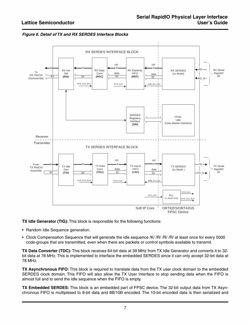
TX SERDES Interface Block
The TX SERDES Interface Block connects this soft IP core to the embedded TX SERDES section of a LatticeORT82G5/ORT42G5 FPSC device. This Interface Block generates the code-group sequences for transmissionwhen neither data nor control symbols are being transmitted. Figure 6 shows the Receive and Transmit side ofSERDES Interface block.
PreviousPacket
ACK ID5
(P)
0003
(P)
Prio2
(P)
TT2
(T)
Ftype4
(L)
TargetAddress8 or 16
(T)
SourceAddress8 or 16
(T)
Transaction4
(L)
Size4
(L)
Source TID8
(L)
Device Offset address32,48,64
(L)
Optional Data Payload8 to 256 bytes
(L)
CRC16(P)
Next Packet
PreviousPacket
ACK ID5
(P)
0003
(P)
Prio2
(P)
TT2
(T)
Ftype4
(L)
TargetAddress8 or 16
(T)
SourceAddress8 or 16
(T)
Transaction4
(L)
Status4
(L)
Target TID8
(L)
Optional Data Payload8 to 256 bytes
(L)
CRC16(P)
Next Packet
(P) – Physical
(T) – Transport
(L) – Logical
7
Serial RapidIO Physical Layer InterfaceLattice Semiconductor User’s Guide
Figure 6. Detail of TX and RX SERDES Interface Blocks
TX Idle Generator (TIG):
This block is responsible for the following functions:
• Random Idle Sequence generation.
• Clock Compensation Sequence that will generate the idle sequence /K/ /R/ /R/ /R/ at least once for every 5000 code-groups that are transmitted, even when there are packets or control symbols available to transmit.
TX Data Converter (TDC):
This block receives 64-bit data at 39 MHz from TX Idle Generator and converts it to 32-bit data at 78 MHz. This is implemented to interface the embedded SERDES since it can only accept 32-bit data at78 MHz.
TX Asynchronous FIFO:
This block is required to translate data from the TX user clock domain to the embeddedSERDES clock domain. This FIFO will also allow the TX User Interface to stop sending data when the FIFO isalmost full and to send the idle sequence when the FIFO is empty.
TX Embedded SERDES:
This block is an embedded part of FPSC device. The 32-bit output data from TX Asyn-chronous FIFO is multiplexed to 8-bit data and 8B/10B encoded. The 10-bit encoded data is then serialized and
RX DataConv(RDC)
RX SERDES(1x Mode)
RX SerialRapidIO
I/F
RDRX ElasticityFIFO(REF) 3232
ctrl
data
TX DataConv(TDC)
TX SERDES(1x Mode )
TX SerialRapidIO
I/F
TDTX AsyncFIFO(TAF) 3232
4ctrl
data
4
64
8
ASB_RX_CLK
ASB_TX_CLK
TX IdleGen(TIG) 64
8
SYS_CLK
SYS_CLK
ctrl
data
SYS_CLK_BY2
SYS_CLK_BY2
ctrl
data
8RX Init
SM(RIS) 6464
8
RD_N
TD_N
PLL(1x Mode Only)
SYS_CLK
SYS_CLK_BY2
SYS_CLK
SERDESRegistersInterface
(SRI)
FPSCUMI
(User Master Interface)
RX SERDES INTERFACE BLOCK
TX SERDES INTERFACE BLOCK
ToRX Pkt/Ctrl
DisAssembly
FromTX Pkt/CtrlAssembly
Receiver
Transmitter
Soft IP Core ORT82F5/ORT42G5FPSC Device
4 4
8
Serial RapidIO Physical Layer InterfaceLattice Semiconductor User’s Guide
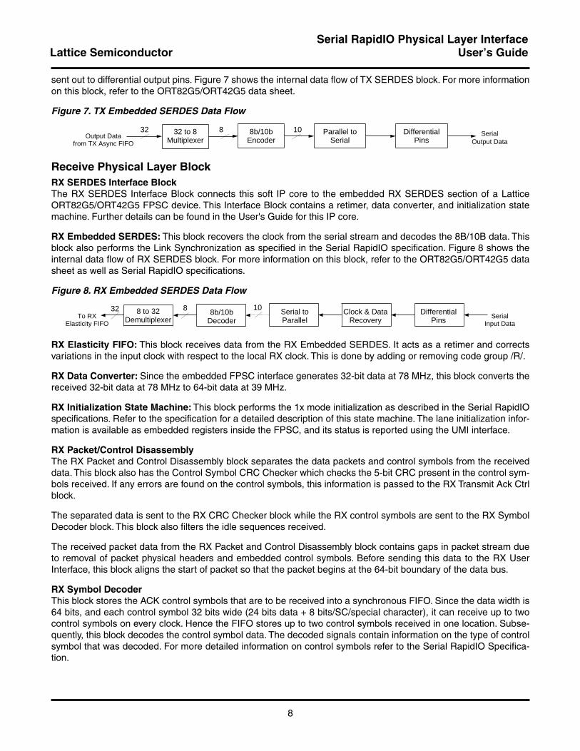
sent out to differential output pins. Figure 7 shows the internal data flow of TX SERDES block. For more informationon this block, refer to the ORT82G5/ORT42G5 data sheet.
Figure 7. TX Embedded SERDES Data Flow
Receive Physical Layer Block
RX SERDES Interface Block
The RX SERDES Interface Block connects this soft IP core to the embedded RX SERDES section of a LatticeORT82G5/ORT42G5 FPSC device. This Interface Block contains a retimer, data converter, and initialization statemachine. Further details can be found in the User's Guide for this IP core.
RX Embedded SERDES:
This block recovers the clock from the serial stream and decodes the 8B/10B data. Thisblock also performs the Link Synchronization as specified in the Serial RapidIO specification. Figure 8 shows theinternal data flow of RX SERDES block. For more information on this block, refer to the ORT82G5/ORT42G5 datasheet as well as Serial RapidIO specifications.
Figure 8. RX Embedded SERDES Data Flow
RX Elasticity FIFO:
This block receives data from the RX Embedded SERDES. It acts as a retimer and correctsvariations in the input clock with respect to the local RX clock. This is done by adding or removing code group /R/.
RX Data Converter:
Since the embedded FPSC interface generates 32-bit data at 78 MHz, this block converts thereceived 32-bit data at 78 MHz to 64-bit data at 39 MHz.
RX Initialization State Machine:
This block performs the 1x mode initialization as described in the Serial RapidIOspecifications. Refer to the specification for a detailed description of this state machine. The lane initialization infor-mation is available as embedded registers inside the FPSC, and its status is reported using the UMI interface.
RX Packet/Control Disassembly
The RX Packet and Control Disassembly block separates the data packets and control symbols from the receiveddata. This block also has the Control Symbol CRC Checker which checks the 5-bit CRC present in the control sym-bols received. If any errors are found on the control symbols, this information is passed to the RX Transmit Ack Ctrlblock.
The separated data is sent to the RX CRC Checker block while the RX control symbols are sent to the RX SymbolDecoder block. This block also filters the idle sequences received.
The received packet data from the RX Packet and Control Disassembly block contains gaps in packet stream dueto removal of packet physical headers and embedded control symbols. Before sending this data to the RX UserInterface, this block aligns the start of packet so that the packet begins at the 64-bit boundary of the data bus.
RX Symbol Decoder
This block stores the ACK control symbols that are to be received into a synchronous FIFO. Since the data width is64 bits, and each control symbol 32 bits wide (24 bits data + 8 bits/SC/special character), it can receive up to twocontrol symbols on every clock. Hence the FIFO stores up to two control symbols received in one location. Subse-quently, this block decodes the control symbol data. The decoded signals contain information on the type of controlsymbol that was decoded. For more detailed information on control symbols refer to the Serial RapidIO Specifica-tion.
32 to 8Multiplexer
8b/10bEncoder
Parallel toSerial
DifferentialPinsOutput Data
from TX Async FIFOSerial
Output Data
32 8 10
8 to 32Demultiplexer
8b/10bDecoder
Serial toParallel
Clock & DataRecovery
DifferentialPinsTo RX
Elasticity FIFOSerial
Input Data
32 8 10

9
Serial RapidIO Physical Layer InterfaceLattice Semiconductor User’s Guide
RX Transmit ACK Control
The RX Transmit ACK control block keeps track of the acknowledgement control symbols for packets transmitted.This is implemented by maintaining an ACK received queue. Once a packet is accepted, an ACK ID number [ACKID = 0 to 31] is sent to the user to release the packet buffer. In the case in which a packet needs to be resent apacket-retry ACK ID [ACK ID = 0 to 31] will be sent to the transmit block to send the packet once again. Similarly,for packets not accepted an ACK ID [ACK ID = 0 to 31] will be sent to the transmit block to resend the packet.
If a packet is still in transmission, a packet-retry or packet-not-accepted acknowledgment may cause the sender tocancel transmission on the packet. The sending device can use the stomp, restart-from-retry (in response to apacket-retry control symbol), or link-request (in response to a packet-not-accepted control symbol) control symbolto cancel the packet.
This block generates appropriate responses to the following control symbol errors. These errors are listed below:
• Error on control symbol– Packet-not-accepted control symbol– Packet-retry/packet-ack control symbol with unexpected ACK ID– Corrupt control symbol
• Time out waiting for control symbol
Retry Recovery:
The retry recovery state machine is part of the RX Transmit ACK Control (RTA) block. Its purposeis to attempt to recover data for a retry condition. It is triggered when a device receives a packet-retry control sym-bol to stop sending new packets. After sending a packet-retry control symbol, the state machine will then send arestart-from-retry control symbol to resend data in which the packet-retry control symbol was sent for.
Figure 9 shows an example of Retry Recovery flow control operation. In this example, after the transmitter trans-mits several packets, the receiver sends a packet-retry control symbol (RetryAck3) on packet #3 to transmitter. Itasks the transmitter to resend packet #3 again. The receiver discards all packets received after packet #3. Oncethe transmitter detects the packet-retry control symbol, it stops sending new packets until it sends an input status ofrestart-from-retry to the receiver to prepare to receive incoming packets.
Figure 9. Retry Recovery Control Data Flow
Transmit ReceivePkt1
Tim
e
Ack1
Pkt3Ack2
Pkt4
Output portstops
sending newpackets
Restart-from-Retry
Input portdiscards all
packetsreceived
Pkt3
Ack3Pkt4
Pkt5
Pkt5
Pkt2
Ack4
Ack5
Retry Ack3

10
Serial RapidIO Physical Layer InterfaceLattice Semiconductor User’s Guide
It is possible that by the time the transmitter receives the packet-retry control symbol (RetryAck3), it is still transmit-ting packet to the receiver due to the transmitter latency to process the packet-retry control symbol. This conditionis fine since the receiver discards all incoming packets received after it sends packet-retry control symbols. Formore information on the retry recovery state machine, refer to the Serial RapidIO specifications
Error Recovery:
The error recovery state machine is also part of RX Transmit ACK Control (RTA) block which hasfunction to attempt to recover data for error conditions. When this state machine detects an output error such as anunexpected ACK ID the state machine immediately transitions into an output error-stopped state and immediatelystops sending new packets and issues a restart-from-error control symbol to the sender. The restart-from-errorcontrol symbol receives a response from the receiver including the ACK ID. This ACK ID indicates where thesender should begin re-transmission. For more information on the error recovery state machine, refer to the SerialRapidIO Specification. Figure 10 shows an example of Error Recovery flow control operation.
Figure 10. Error Recovery Flow Diagram
RX Receive Packet ACK Control
The RX Receive Packet ACK Control block generates the ACK control symbols for the packets received.
The different packet errors are as follows:
• Unexpected ACK ID on packets
• Corrupt packet indicated by CRC
• Packet that overruns defined packet boundary
When this block detects an error on a packet (CRC error/unexpected ACK ID value/over running the maximum datapayload) it immediately transitions into an input error-stopped state and silently discards all new packets until itreceives a restart-from-error control symbol from the sender. The state machine also sends a control symbol withthe received ACK ID value back to the sender, which indicates that the packet is not accepted. The sender then ini-tiates recovery by resending of the packet.
This block uses the error recovery and retry recovery state machines, similar to the ones defined in the RX ReceiveTransmit ACK block.
Transmit ReceivePkt1
Tim
e
Ack1Pkt2
Pkt3(Err) Ack2
Pkt4
Output portstops
sending newpackets
Input portdiscards all
packetsreceived
Pkt3
Ack3Pkt4
Pkt5
Link Response
Not Accepted Ack3
Restart-from-error

11
Serial RapidIO Physical Layer InterfaceLattice Semiconductor User’s Guide
RX CRC Checker
The RX CRC Checker generates a separate CRC for each data packet and compares it to the appended CRCtransmitted with each packet, to determine any errors.
The CRC is generated for the packet header and the entire data payload, with the exception of the first 6 bits of theadded physical layer fields (which are treated as logical 0’s). The initial value of the CRC is 0xFFFF. For the CRCcalculation, the first 6 bits (ACK ID field and first bit of reserved field) are assumed to be logic zero. This structureallows the ACK ID to be changed on a link-by-link basis as the packet is transported, without requiring the CRC tobe recomputed for each link.
Figure 11 shows the format of packet with CRC.
Figure 11. CRC Checking
The leading 16 bits of the packet are referred to as the first symbol of the packet. The first symbol of a packet shallalways land on the most significant half of the 32-bit boundary.
For a packet that has less than or equal to 80 bytes of header (including all logical, transport, and 8/16 LP-LVDSfields) and logical data payload, a single CRC value is appended to the packet.
For packets with greater than 80 bytes (including physical layer header and logical data payload) a CRC value isinserted after the first 80 bytes, aligning it to the first half of the 32-bit alignment boundary, and a second CRC valueis appended at the end of the packet. The second CRC value is a continuation of the first and included in the run-ning calculation, meaning that the running CRC value is not re-initialized after it is inserted after the first 80 bytes ofthe packet.
This allows the devices to regard the embedded CRC value as two bytes of packet payload for CRC checking pur-poses. If the final appended CRC value does not cause the total packet to align to the 32-bit boundary, a 2-byte padof all logic 0’s is post appended to the packet. The pad of logic 0’s allows the CRC check to always be done at the32-bit boundary.
RX User Interface
The RX User Interface generates all the control signals necessary to interface to the RX user logic or the Logicaland Transport layers of the RapidIO stack. This block generates the signals indicating that the RX PHY is ready tosend data. This block also controls the discard signal, which is used to discard a packet being sent to the user logicif packet errors are detected.
The block is used by the user logic to receive data and core status from the Serial RapidIO core, and to interface toa simple FIFO interface. The signals generated/used by this block are described in the User Interface section andthe Signal Description section of this document.
User Interface
This section explains in detail the user interface signals that are present in this Serial RapidIO PHY IP. The follow-ing are the different user interfaces:
• TX User Interface
• RX User Interface
• PMI Interface
Protected by CRC
ACKID5
01
002
Prio2
TT2
Ftype4
Remainder of Transport & Logical fieldn*16
CRC Value16
Protected by protocol

12
Serial RapidIO Physical Layer InterfaceLattice Semiconductor User’s Guide
TX User Interface
The TX User Interface consists of two types of interface: TX User Control Interface and TX Generic FIFO BridgeInterface. Both run synchronously with the system clock
sys_clk
signal.
The TX User Control Interface generates all the control signals required for the TX user such as
tx_rios_ready
,
tx_next_ackid
,
tx_release_ackid
,
tx_rios_discard
and
tx_release_val
. The TX Generic FIFOBridge Interface is a standard FIFO interface used to manage the data flow coming from the user side (signalsbeginning with “
sine_tx_
”).
After the device is powered up and
reset_n
signal is asserted, the Serial RapidIO core goes through an internalinitialization cycle. During this time, the core initializes the ORT82G5/ORT42G5 SERDES registers, checkswhether the SERDES Receive channel is synchronized and performs 1x initialization. Once this is successful, the
tx_rios_ready
signal is asserted indicating that the core is ready for transmitting Serial RapidIO packets.
Note:
During the transmit process, the status of
tx_rios_ready
must be monitored at all times. Whentx_rios_ready is de-asserted, all user interface signals should be regarded as invalid input or invalid output.
Once the tx_rios_ready is asserted, the tx_next_ackid[4:0] indicates the ACK ID of the buffer to be trans-mitted. These buffers are numbered from 0 to 31 and are maintained by the user. Each of these buffers contains apacket that has to be transmitted through the Serial RapidIO core. The implementation of these buffers is left to theuser and is not specified by this document.
If a packet has been successfully transmitted by the core, i.e. after the core receives an acknowledgement from thefar end receiver, the signal tx_release_val goes active indicating that the user buffer associated with thetx_release_ackid[4:0] value can be released. This means that the user can now store a different packet intothe buffer that has been released. The buffer should not be updated with a new packet until a release signaltx_release_ackid has been received on that buffer.
Once a complete packet is available at the user end for transmission, the user has to indicate this to the core byasserting the sine_tx_data_avail signal. On seeing the sine_tx_data_avail signal active, the core acti-vates the read signal sine_tx_read.
Once the sine_tx_read is activated, the user should provide the requested buffer data on these signals. Theother signals associated with this data transfer are tx_prio[1:0], sine_tx_sof, sine_tx_data[63:0],sine_tx_data_en[3:0] and sine_tx_eof.
The sine_tx_sof signal should be asserted at the start of the packet and sine_tx_eof should be asserted atthe end of the packet. The sine_tx_sof signal should only be asserted for one clock cycle. Whensine_tx_read is asserted, it initiates the packet transfer while the core is waiting for this signal asserted. As soonas it detects the sine_tx_sof asserted, it immediately goes to the next step of the internal processing algorithm.
The tx_prio[1:0] indicates the priority field of the Serial RapidIO packet. The sine_tx_data_en[3:0] indi-cates valid half word of the sine_tx_data of the current packet transfers.
The sine_tx_alm_empty signal should be asserted whenever the buffer contains only one 64-bit data left. Thissignal is used to deactivate the sine_tx_read signal to prevent the core from issuing illegal reads.
During a data transfer from the user side to the core, i.e. when sine_tx_read is active, the user can terminate thetransfer by activating the tx_usr_discard. Similarly the core can terminate the packet by activating thetx_rios_discard. The reasons on which the user can terminate the packet transfer are user implementationdependent and are not specified by this document.
RX User InterfaceThe RX User Interface consists of RX User Control Interface and RX Generic FIFO Bridge Interface. Both run syn-chronously with the system clock sys_clk signal. The RX User Control Interface generates all the control sig-nals required for the RX user such as rx_rios_ready and rx_rios_discard. The RX Generic FIFO Bridge

13
Serial RapidIO Physical Layer InterfaceLattice Semiconductor User’s Guide
Interface is a standard FIFO interface used to manage the data flow going to the user logic side (signals beginningwith “sine_rx_”).
After the device is powered up and reset_n signal is activated, the Serial RapidIO core goes through an internalinitialization cycle, during which the core initializes the ORT82G5/ORT42G5 SERDES registers, checks the syn-chronization of SERDES Receive Channel and performs 1x initialization. Once this is successful therx_rios_ready signal goes active indicating that the other control signals on the RX interface are valid.
After the rx_rios_ready is active, whenever the core receives a good packet, the core generates asine_tx_write signal indicating that the data transfer to the user is active. The other signals associated with thisdata transfer are: sine_rx_sof, sine_rx_data[63:0], sine_rx_hwen[3:0] and sine_rx_eof.
The sine_rx_sof signal will always be asserted at the start of the packet to indicate the beginning of new packet.However, for the end of the packet case, the sine_rx_eof signal may or may not be asserted.
There are two conditions indicating that the transfer of one packet has ended:
1. The assertion of the sine_rx_eof signal at the end of the packet.
2. The assertion of the sine_rx_sof signal to indicate that a new packet is started and the previous packet has been ended.
The sine_rx_hwen[3:0] indicates the valid half word of the data bus sine_rx_data of the current packettransfer. When the packet is being transferred, invalid and valid data could be sent on the same packet. Thus, it isimportant for user to use both sine_rx_hwen[3:0] signals and sine_rx_data bus together to determine thevalidity of data in the current packet.
During a data transfer from the core to the user side, i.e. when sine_rx_write is active, the user can terminatethe transfer by activating the rx_usr_discard. Similarly the core can terminate the packet by activating therx_rios_discard. The reasons on which the user can terminate the packet transfer are user implementationdependent and are not specified by this document.
The user also provides the rx_buf_status[4:0] signal which indicates number of available packet buffers inuser logic. Encoding value specifies the number of packet buffers the receiving device has currently available. Thevalue “00000” specifies buffer is full, “11110” specifies 30 spaces available and “11111” specifies undefined num-ber of spaces available. The core uses this buffer status signal whenever a control symbol is generated and sentout.
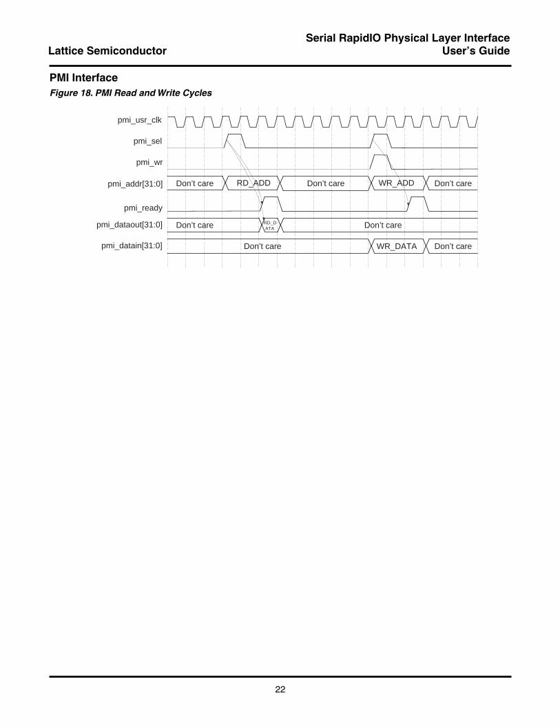
PMI InterfaceThe Physical Layer Management Interface (PMI) is used to read the registers present in the IP and the registerspresent in the ORT82G5/ORT42G5 embedded SERDES block.
This interface uses a separate clock signal called pmi_usr_clk. Thus, the interface can run independently and ata different frequency compared to Transmit or Receive blocks in the core.
After the device is powered up and has gone through a reset cycle using the reset_n signal, the pmi_ready sig-nal will be inactive indicating to the user that the interface is ready to accept read/write cycles.
Once the pmi_ready is deasserted or inactive, user can perform a read operation by pulsing the pmi_sel signalalong with the pmi_addr signal which contains the address of the register to be read, and the signal pmi_wrshould be active low indicating a read command. After the above sequence the user logic should wait for thepmi_ready signal to go high indicating successful completion of the read cycle and the data read out from the reg-ister will be available on the pmi_dataout[31:0] data bus.
To perform a write cycle the user logic first has to check if the pmi_ready is low. After that, the write operation canbe performed by pulsing the pmi_sel signal along with the pmi_addr which contains the address of the register tobe written. The bus pmi_datain[31:0] should contain the data to be written into the register and the pmi_wr

14
Serial RapidIO Physical Layer InterfaceLattice Semiconductor User’s Guide
signal should be active high indicating a write command. After the above sequence, the user logic should wait forthe pmi_ready signal to go high indicating successful completion of the write cycle. The data onpmi_datain[31:0] bus should remain valid during the pmi_ready signal asserted.
Register DescriptionsThis section describes the different registers available in this core. Table 2 shows the overall global memory map ofthe IP and different register sets implemented.
Table 2. Register Memory MAP
Table 3 shows different PHY CSR registers implemented in this core.
Table 3. PHY CSR Registers
Table 3a. PHY_HEADER0
Table 3b. PHY_HEADER1
Table 3c. PHY_LINK_TO
Address Description
USR_RIOPHY_BASE +16’h0xxx PHY CSR Registers. These implement the PHY Command and Status Reg-isters as defined in the Serial RapidIO Specification.
USR_RIOPHY_BASE +16’h1xxx User Registers. These implement the registers required by the core, and gives status information about the core.
USR_RIOPHY_BASE +16’h2xxx SERDES Registers. For SERDES Registers please refer to the ORT42G5/ORT82G5 FPSC data sheet available at www.latticesemi.com.
Offset Address Name Description
‘h000 PHY_HEADER0 Port Maintenance Block Header 0
‘h004 PHY_HEADER1 Port Maintenance Block Header 1
‘h020 PHY_LINK_TO Port Link Time-Out Control CSR
‘h024 PHY_RESP_TO Port Response Time-Out Control CSR
‘h03C PHY_GEN_CTL Port General Control CSR
‘h058 PHY_ERR_STAT Port Error and Status CSR
‘h05C PHY_CONTROL Port 0 Control CSR
Name Bits Reset Value Access Description
EF_PTR 15:0 'EF_PTR R Hard wired pointer to the next block in the data structure, if one exists
EF_ID 31:16 ‘h0001 R Hard wired Extended Features ID
Name Bits Reset Value Access Description
— 31:0 — — Reserved
Name Bits Reset Value Access Description
link_time_out 23:0 ‘hFFFF RW Time-out interval value
— 31:24 — — Reserved

15
Serial RapidIO Physical Layer InterfaceLattice Semiconductor User’s Guide
Table 3d. PHY_RESP_TO
Table 3e. PHY_GEN_CTL
Name Bits Reset Value Access Description
resp_time_out 23:0 ‘hFFFF RW Time-out interval value
— 31:24 — — Reserved
Name BitsReset Value Access Description
host 0 0 RW
A Host device is a device that is responsible for system exploration, initialization, and maintenance. Agent or slave devices are typically initialized by Host devices. ‘b0 - agent or slave device ‘b1 - host device
master_enable 1 0 RW
The Master Enable bit controls whether or not a device is allowed to issue request into the system. If the Master Enable is not set, the device may only respond to requests. ‘b0 - processing element cannot issue request ‘b1 - processing element can issue requests
discovered 2 0 RW
This device has been located by the processing element responsible for system configuration. ‘b0 - The device has not been previously discovered ‘b1 - The device has been discovered by another processing element
- 31:3 - - Reserved
Table 3f. PHY_ERR_STAT
Name BitsReset Value Access Description
— 10:0 — — Reserved
output_retry_enc 11 0 RW Output port has encountered a retry condition. This bit is set until written with a logic 1 to clear.
output_retried 12 0 R
Output port has received a packet-retry control symbol and cannot make progress. This bit is set when bit 13 is set and is cleared when a packet-accepted or a packet-not-accepted control symbol is received.
output_retry_stop 13 0 R Output port has received a packet-retry control symbol and is in the output-retry-stopped state.
output_err_enc 14 0 RWOutput port has encountered (and possibly recovered from) a transmission error. This bit is set when bit 15 is set. Once set, it remains set until written with a logical 1 to clear.
output_err_stop 15 0 R Output port is in the output error-stopped state.
- 20:16 — — Reserved
input_retry_stop 21 0 R Input port is in the input retry-stopped state.
input_err_enc 22 0 RWInput port has encountered (and possibly recovered from) a transmission error. This bit is set when bit 23 is set. Once set, it remains set until written with a logic 1 to clear.
input_err_stop 23 0 R Input port is in the input error-stopped state.
— 26:24 — — Reserved
port_write_pend 27 0 RW
Port has encountered a condition, which required it to initiate a Maintenance Port-write transaction. This bit is only valid if the device is capable of issuing a maintenance port -write transaction. Once set, it remains set until written with a logic 1 to clear.
16
Serial RapidIO Physical Layer InterfaceLattice Semiconductor User’s Guide
— 28 — — Reserved
port_error 29 0 RWInput or output port has encountered an error from which hardware was unable to recover. Once set, it remains set until written with a logic 1 to clear.
port_ok 30 0 RInput and output ports are initialized and can communicate with the adjacent device. This bit and bit 31 are mutually exclusive.
port_uninit 31 1 R Input and output ports are not initialized and is in training mode. This bit and bit 30 are mutually exclusive.
Table 3g. PHY_CONTROL
Name BitsReset Value Access Description
port_width 1:0 00 R
Operating width of the port: 00 Single Lane 10 Four Port 01-11 Reserved
initialized_port_width 4:2 000 R
Init Port width: 000 Single port Lane 0 100 Single Port Lane 2 010 Four Port Lane 110-111 Reserved
port_width_override 7:5 000 RW
Soft port Config Override: 000 No override100 Reserved 010 Force single lane Lane 0 110 Force single lane Lane 2 001-111 Reserved
port_disable 8 0 R/WPort Disable: 0 Disable Receiver/driver 1 Disable Receiver/driver
output_port_en 9 0 RW
Output port transmit enable: 0 - port is stopped and only enabled to route or respond I/O logical MAINTENANCE packets, depending upon the functionality of the processing element. Control symbols are not affected and are received and handled normally. 1 - port is enabled to respond to any packet
input_port_en 10 0 RW
Input port receive enable: 0 - port is stopped and only enabled to route or respond I/O logical MAINTENANCE packets, depending upon the functionality of the processing element. Other packets generate packet-not-accepted control symbols to force an error condition to be signaled by the sending device. Control sym-bols are not affected and are received and handled normally. 1 - port is enabled to respond to any packet
err_chk_dis 11 0 RW
This bit disables all RapidIO transmission error checking: 0 - Error checking and recovery is enabled 1 - Error checking and recovery is disabled Device behavior when error checking and recovery is dis-abled and an error condition occurs is undefined
Table 3f. PHY_ERR_STAT (Continued)
Name BitsReset Value Access Description

17
Serial RapidIO Physical Layer InterfaceLattice Semiconductor User’s Guide
The following table shows the different USER registers implemented in this core.
Table 4. User Registers
Table 4a. USR_STATUS
Table 4b. USR_SYMBOL
multicast_partp 9 0 R Send incoming multicast-event control symbols to this port (multi port devices only)
— 30:13 — — Reserved
port_type 31 1 RThis indicates the port type, parallel or serial: 0 - Parallel port 1 - Serial port
Offset Address Name Description
‘h000 USR_STATUS Status Register
‘h004 USR_SYMBOL Symbol register
‘h008 USR_RETRANS_CNTMaximum number of times a packet can be retransmitted when packet is not accepted.
Name BitsReset Value Access Description
force_reinit 0 0 RW For initialization, force_reinit to be written with logic 1. When initialization is complete, force_reinit will return logic 0.
err_ackid 1 0 RW Indicates Link Response Fatal Error. The link response contains the ACKID that is not outstanding
cs_sent 2 1 R Requested Control Symbol is sent
init_done 3 0 W Management configured the registers, so that ports are ready
reset_cs 4 0 RW Reset control symbol received
naccptd_cause
9:5 0 R
Displays reasons why packet not accepted: 00000: Reserved 00001: Received unexpected ACKID on packet 00010: Received a control symbol with bad CRC 00011: Non-maintenance packet reception is stopped 00100: Received packet with bad CRC 00101: Received invalid character, or valid but illegal character11110: Reserved 11111: General error
mc_event 10 0 R/W MC event received, set by core cleared by user.
— 31:11 — — Reserved
Name BitsReset Value Access Description
cs 5:0 ‘h0000 RW Control symbol that need to be sent (given by the user)
— 31:6 - — Reserved
Table 3g. PHY_CONTROL (Continued)
Name BitsReset Value Access Description

18
Serial RapidIO Physical Layer InterfaceLattice Semiconductor User’s Guide
Table 4c. USR_RETRANS_CNT
Name BitsReset Value Access Description
retrans_cnt 2:0 ‘h7 RW Maximum number of times a packet can be retransmitted when packet is not accepted
— 31:3 — — Reserved

19
Serial RapidIO Physical Layer InterfaceLattice Semiconductor User’s Guide
Timing DiagramsTransmit User InterfaceFigure 12. TX User Data Transfer of a Packet
Figure 13. TX Discarding a Packet by tx_usr_discard
sys_clk
tx_rios_ready
tx_rios_discard
tx_usr_discard
sine_tx_sof
sine_tx_eof
tx_release_val
4’h0tx_release_ackid[4:0]
tx_next_ackid[4:0] 5’d1
sine_tx_data_avail
sine_tx_read
5’d2
h0,d1,d2,d3
d4,d5,d6,d7 .... d26,d27
d28,d29d30,d31
,0,0
4’hF 4’hF .... 4’hF 4’hC
h0, d1, d2, d3
F
5’d3
h0,d1,d2,d3
d4,d5,d6,d7 .... ....
4’hF 4’hF 4’hF 4’hF
....
4’hF
sine_tx_alm_empty
sine_tx_data_en[3:0]
sine_tx_data[63:0]
sys_clk
tx_rios_ready
tx_rios_discard
tx_usr_discard
sine_tx_sof
sine_tx_eof
tx_release_val
4’h0tx_release_ackid[4:0]
tx_next_ackid[4:0] 5’d1
sine_tx_data_avail
sine_tx_read
5’d2
h0,d1,d2,d3
d4,d5,d6,d7 .... .... ....
4’hF 4’hF 4’hF 4’hF 4’hF F
5’d1
h0,d1,d2,d3
d4,d5,d6,d7 .... ....
4’hF 4’hF 4’hF 4’hF
....
4’hF
sine_tx_alm_empty
5’d2
....
4’hF
....
4’hF
Don’t care
Don’t care
sine_tx_data[63:0]
sine_tx_data_en[3:0]

20
Serial RapidIO Physical Layer InterfaceLattice Semiconductor User’s Guide
Figure 14. TX Discarding a Packet by tx_rios_discard
Receive User InterfaceFigure 15. RX Transfer of Data Without Discards
sys_clk
tx_usr_discard
tx_rios_discard
sine_tx_sof
sine_tx_eof
tx_release_val
4’h0tx_release_ackid[4:0]
tx_next_ackid[4:0] 5’d1
sine_tx_data_avail
sine_tx_read
5’d2
h0,d1,d2,d3
d4,d5,d6,d7 .... .... ....
4’hF 4’hF 4’hF 4’hF 4’hF
5’d1
h0,d1,d2,d3
d4,d5,d6,d7 .... ....
4’hF 4’hF 4’hF 4’hF
....
4’hF
sine_tx_alm_empty
5’d2
....
4’hF
tx_rios_ready
sine_rx_data[63:0]
sine_rx_data_en[3:0]
don’t care
don’t care
sys_clk
rx_rios_ready
rx_rios_discard
rx_usr_discard
rx_buf_status[4:0]
sine_rx_sof
sine_rx_eof
h0,d1,d2,d3
5’d20 5’d19
sine_rx_write
d4,d5,d6,d7 .... .... .... .... ....
4’hF 4’hF 4’hf 4’hf 4’hf 4’hF 4’hF/4’h0
sine_rx_data[63:0]
sine_rx_hwen[3:0]
don’t care
don’t care

21
Serial RapidIO Physical Layer InterfaceLattice Semiconductor User’s Guide
Figure 16. Discarding the Packet using rx_rios_discard
Figure 17. Discarding the Packet using rx_usr_discard
sys_clk
rx_rios_ready
rx_usr_discard
rx_rios_discard
rx_buf_status[4:0]
sine_rx_sof
sine_rx_eof
h0,d1,d2,d3
5’d20
sine_rx_write
d4,d5,d6,d7 .... .... .... .... ....
4’hF 4’hF 4’hF 4’hF 4’hF 4’hF 4’hF
.... .... ....
4’hF 4’hF 4’hF
sine_rx_data[63:0]
sine_rx_hwen[3:0]
sys_clk
rx_rios_ready
rx_rios_discard
rx_usr_discard
rx_buf_status[4:0]
sine_rx_sof
sine_rx_eof
h0,d1,d2,d3
5’d20
sine_rx_write
d4,d5,d6,d7 .... .... .... .... ....
4’hF 4’hF 4’hF 4’hF 4’hF 4’hF 4’hF
.... .... ....
4’hF 4’hF 4’hF
sine_rx_data[63:0]
sine_rx_hwen[3:0]
22
Serial RapidIO Physical Layer InterfaceLattice Semiconductor User’s Guide
PMI InterfaceFigure 18. PMI Read and Write Cycles
pmi_usr_clk
pmi_sel
pmi_addr[31:0]
pmi_ready
pmi_dataout[31:0]
pmi_wr
pmi_datain[31:0]
RD_ADD
RD_DATA
WR_ADD
WR_DATA
Don’t care Don’t care Don’t care
Don’t care
Don’t care Don’t care
Don’t care
23
Serial RapidIO Physical Layer InterfaceLattice Semiconductor User’s Guide
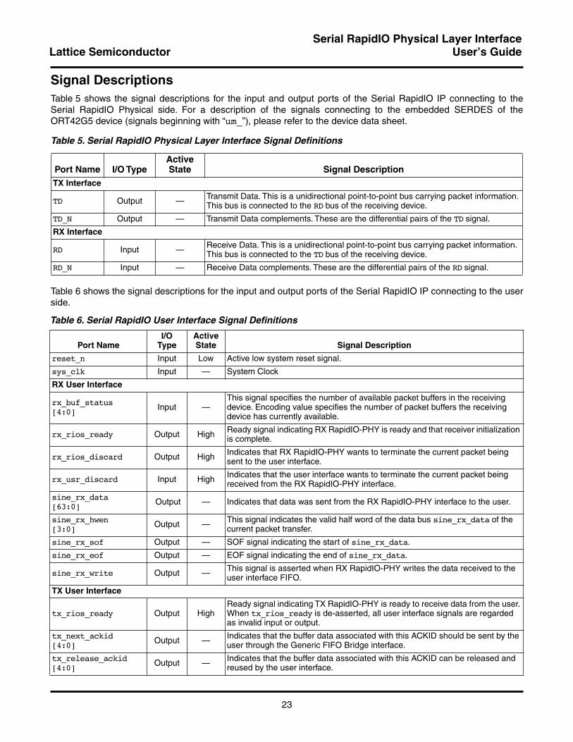
Signal DescriptionsTable 5 shows the signal descriptions for the input and output ports of the Serial RapidIO IP connecting to theSerial RapidIO Physical side. For a description of the signals connecting to the embedded SERDES of theORT42G5 device (signals beginning with “um_”), please refer to the device data sheet.
Table 5. Serial RapidIO Physical Layer Interface Signal Definitions
Table 6 shows the signal descriptions for the input and output ports of the Serial RapidIO IP connecting to the userside.
Port Name I/O TypeActive State Signal Description
TX Interface
TD Output — Transmit Data. This is a unidirectional point-to-point bus carrying packet information. This bus is connected to the RD bus of the receiving device.
TD_N Output — Transmit Data complements. These are the differential pairs of the TD signal.
RX Interface
RD Input — Receive Data. This is a unidirectional point-to-point bus carrying packet information. This bus is connected to the TD bus of the receiving device.
RD_N Input — Receive Data complements. These are the differential pairs of the RD signal.
Table 6. Serial RapidIO User Interface Signal Definitions
Port NameI/O
TypeActiveState Signal Description
reset_n Input Low Active low system reset signal.
sys_clk Input — System Clock
RX User Interface
rx_buf_status[4:0]
Input —This signal specifies the number of available packet buffers in the receiving device. Encoding value specifies the number of packet buffers the receiving device has currently available.
rx_rios_ready Output High Ready signal indicating RX RapidIO-PHY is ready and that receiver initialization is complete.
rx_rios_discard Output High Indicates that RX RapidIO-PHY wants to terminate the current packet being sent to the user interface.
rx_usr_discard Input High Indicates that the user interface wants to terminate the current packet being received from the RX RapidIO-PHY interface.
sine_rx_data[63:0]
Output — Indicates that data was sent from the RX RapidIO-PHY interface to the user.
sine_rx_hwen[3:0]
Output — This signal indicates the valid half word of the data bus sine_rx_data of the current packet transfer.
sine_rx_sof Output — SOF signal indicating the start of sine_rx_data.
sine_rx_eof Output — EOF signal indicating the end of sine_rx_data.
sine_rx_write Output — This signal is asserted when RX RapidIO-PHY writes the data received to the user interface FIFO.
TX User Interface
tx_rios_ready Output HighReady signal indicating TX RapidIO-PHY is ready to receive data from the user. When tx_rios_ready is de-asserted, all user interface signals are regarded as invalid input or output.
tx_next_ackid[4:0]
Output — Indicates that the buffer data associated with this ACKID should be sent by the user through the Generic FIFO Bridge interface.
tx_release_ackid[4:0]
Output — Indicates that the buffer data associated with this ACKID can be released and reused by the user interface.

24
Serial RapidIO Physical Layer InterfaceLattice Semiconductor User’s Guide
tx_rios_discard Output High Indicates that TX RapidIO-PHY wants to terminate the current packet being received from the user interface.
tx_usr_discard Input High Indicates the user interface wants to terminate the current packet being sent to the RapidIO-PHY interface.
tx_prio[1:0] Input — Indicates the priority of the packet being received.
tx_release_val Output — Indicates that tx_release_ackid is valid.
sine_tx_data[63:0]
Input — Indicates that data was received from the user interface.
sine_tx_alm_empty Input High This signal is asserted when the user transmit FIFO is almost empty. The threshold is set to one 64 bit.
sine_tx_read Output High This signal is asserted when the TX RapidIO PHY requests data from the user transmit FIFO.
sine_tx_sof Input High This signal is asserted with the first data transferred to indicate the start of a new packet. It should be asserted for a maximum of one clock cycle.
sine_tx_eof Input High This signal is asserted with the last data transferred to indicate the end of the packet.
sine_tx_data_en[3:0]
Input — This signal indicates the valid half word of the data bus on the last data transfer of the current packet.
sine_tx_data_avail Input High This signal is asserted as long as there is one full packet or predetermined amount of data in the user transmit FIFO.
PMI Interface
pmi_usr_clk Input — Management interface clock
pmi_sel Input High Management Device Select - This signal is asserted to access Management registers.
pmi_ready Output High Indicates when Management is ready. This signal is asserted to indicate that Management has taken/kept the data from/to the data bus.
pmi_wr Input High Management register write. Valid when pmi_sel is asserted. When this signal is low, it indicates a read.
pmi_addr[31:0] Input — Management address bus for register access.
pmi_datain[31:0] Input — Register Data In
pmi_dataout[31:0] Output — Register Data Out
pmi_int Output High Management Interrupt
Table 6. Serial RapidIO User Interface Signal Definitions (Continued)
Port NameI/O
TypeActiveState Signal Description

25
Serial RapidIO Physical Layer InterfaceLattice Semiconductor User’s Guide
User Configurable ParametersUser configurable parameters are shown below in Table 7. These parameters are configured using IPexpress™,included with Lattice's ispLEVER® design tools.
Table 7. User Configurable Parameters
Parameter Description Range Default
Device Type Target device selection [Pre-selected]ORT42G5
[Pre-selected]ORT42G5
Phy Base Address PMI Phy Register Base Address 0 - FFFF_FFFF 32’h0000_0000
EF_PTR (CSR Block Header0) EF Pointer in CSR Block Header0 0-FFFF 16’h0000
Silence Timer
Silence Timer Count Value: This is the dura-tion of the SILENT state. The duration must be long enough to ensure that the link partner detects the silence (as a loss of lane sync) and is forced to initialize but short enough that it is readily distinguished from a link break. Refer to Serial RapidIO Specification for further informa-tion on the SILENT state section 4.6.3.5
FF-FFFF 16’h00FF
Max. Packet Size in bytes
Maximum Byte Size per Packet: This sets the maximum packet size in bytes that the receiver can accept. Any packets above the maximum packet size will be discarded by the receiver
8-508 276
Receive Nop Limit
Number of Maximum Idle Control Symbols to be Received: This sets a limit on the maxi-mum number of IDLE control symbols that can be received within a packet. Any number of idles above the maximum size will cause the packet to be discarded by the receiver
1-FF FF

26
Serial RapidIO Physical Layer InterfaceLattice Semiconductor User’s Guide
Figure 19. Serial RapidIO Parameter Configuration Dialog Box
References• ispLEVER® Software Online Help Manual
• IP Evaluation Tutorials
Technical Support AssistanceHotline: 1-800-LATTICE (North America)
+1-503-268-8001 (Outside North America)
e-mail: [email protected]
Internet: www.latticesemi.com
27
Serial RapidIO Physical Layer InterfaceLattice Semiconductor User’s Guide
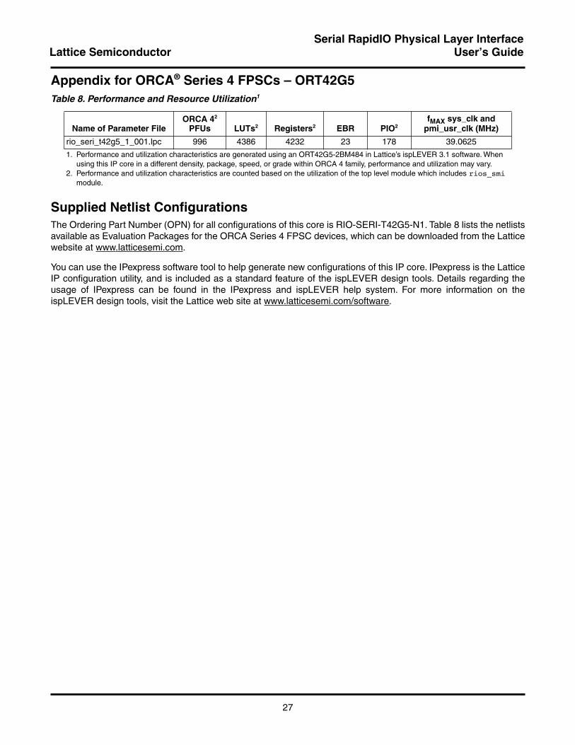
Appendix for ORCA® Series 4 FPSCs – ORT42G5Table 8. Performance and Resource Utilization1
Supplied Netlist ConfigurationsThe Ordering Part Number (OPN) for all configurations of this core is RIO-SERI-T42G5-N1. Table 8 lists the netlistsavailable as Evaluation Packages for the ORCA Series 4 FPSC devices, which can be downloaded from the Latticewebsite at www.latticesemi.com.
You can use the IPexpress software tool to help generate new configurations of this IP core. IPexpress is the LatticeIP configuration utility, and is included as a standard feature of the ispLEVER design tools. Details regarding theusage of IPexpress can be found in the IPexpress and ispLEVER help system. For more information on theispLEVER design tools, visit the Lattice web site at www.latticesemi.com/software.
Name of Parameter FileORCA 42
PFUs LUTs2 Registers2 EBR PIO2fMAX sys_clk and
pmi_usr_clk (MHz)
rio_seri_t42g5_1_001.lpc 996 4386 4232 23 178 39.0625
1. Performance and utilization characteristics are generated using an ORT42G5-2BM484 in Lattice’s ispLEVER 3.1 software. When using this IP core in a different density, package, speed, or grade within ORCA 4 family, performance and utilization may vary.
2. Performance and utilization characteristics are counted based on the utilization of the top level module which includes rios_smi module.

Mouser Electronics
Authorized Distributor
Click to View Pricing, Inventory, Delivery & Lifecycle Information: Lattice:
RIO-SERI-T42G5-N1