sequential mos logic circuits a. marzuki. introduction behavior of bistable elements sr latch...
TRANSCRIPT

Sequential MOS Logic Circuits
A. Marzuki

Introduction
•Behavior of Bistable Elements
•SR Latch Circuit
•Clocked Latch and Flip Flop Circuits
•CMOS D-Latch and Edge-Triggered Flip-Flop
•Sequential Circuit

Classification of logic circuits based on temporal behaviour

Sequential circuit
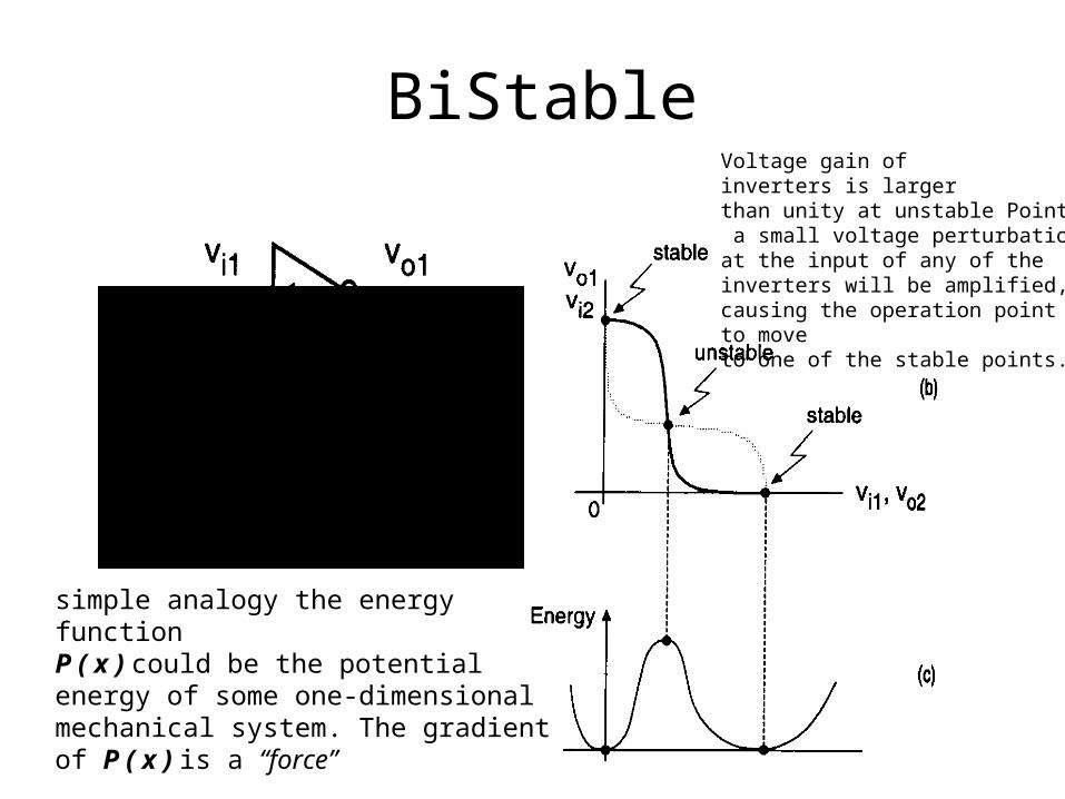
BiStableVoltage gain of inverters is larger than unity at unstable Point, a small voltage perturbation at the input of any of the inverters will be amplified, causing the operation point to moveto one of the stable points.
simple analogy the energy functionP ( x ) could be the potential energy of some one-dimensionalmechanical system. The gradient of P ( x ) is a “force”

Bistable
where gm = (gmN + gmP ) : All four Transistor are in saturation
At V01 = V02 Unstable condition
Output Expectation(exponential!!!)
Directionis determinedby initial perturbation polarity.

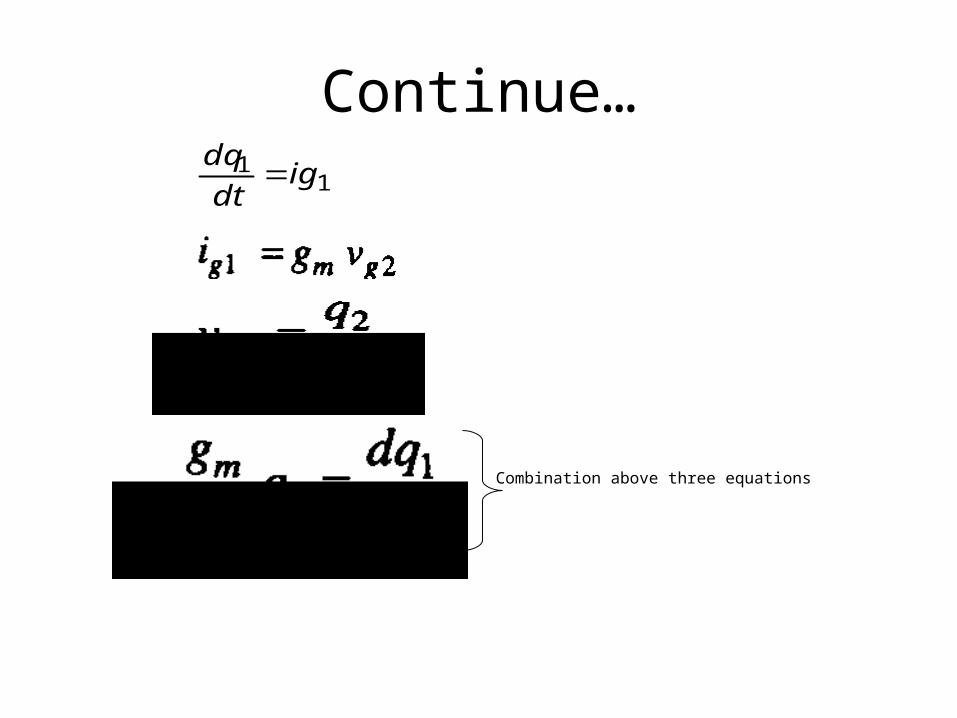
Continue…Gate Capacitance >>> Drain Capacitance
Gate Charges
Derivative of small-signal gate voltages
Continue…1
1 igdt
dq
Combination above three equations

Continue…
Combination of two equation yields 2nd order differential equation
Time behaviour of gate charge q1

Continue…

Continue…

Continue…
Assume ~ Large t
SR Latch Circuit

Gate-level Schematic/Block Diagram.

Truth Table
Operation Mode

Capacitance

Circuit with Capacitance

Rise Time

Depletion Load nMOS (NOR2)

CMOS SR Latch circuit (NAND2)

Gate Schematic(NAND)

Truth Table

Depletion Load nMOS (NAND)

Clocked Latch and Flip-Flop Circuits

Sample Input-Output Waveforms

AOI Implementation (NOR)

Gate Schematic (NAND), active low

Gate Schematic (NAND), active high

Partial Block Diagram

Gate Schematic

Block Diagram

All NAND Implementation

Detailed Truth Table
• J, K Compliments Q will go to J value at the next clock edge. J, K HIGH, the output will reverse its state after each clock pulse.

NOR-based JK Latch

AOI Realization(NOR)

Toggle Switch

Master-Slave Flip Flop

Master-Slave Flip Flop

Master-Slave Flip Flop (NOR)
• CLK is HIGH MASTER is enable. Slave is disable and retains its previous state.
• CLK is LOW is disconnected while input of slaves are simultaneously coupled to the output of the slaves.
CMOS D-Latch and Edge-Triggered Flip Flop

CMOS Implementation

Simplified Schematic View

Timing Diagram

2nd CMOS Implementation

CMOS –ve Edge-triggered

Simulated Input-Output

Timing Violation

Layout

CMOS +ve Edge-triggered

Timing Diagram

References
• Metastability Behavior of CMOS ASIC Flip-Flops in Theory and Test, JENS U. HORSTMANN, JSSC, FEB 1989.
• S-M. Kang and Y. Leblebici ,CMOS Digital Integrated Circuits: Analysis and Design,, 3rd edition