september 8-14, 2016, cluj-napoca, romania · september 8-14, 2016, cluj-napoca, romania . ......
TRANSCRIPT

September 8-14, 2016, Cluj-Napoca, Romania
PAMS-2 2nd Autumn School on on Physics of Advanced
Materials
September 8-14, 2016, Cluj-Napoca, Romania www.icpam.ro
Daily Program and Abstracts
Sebastian Popescu
Mihaela Irimia Mihaela Toma George Rusu

2
Cover: Dragos Dutu

3
Foreword
In 2012, september 22-28, the 10th International Conference on Physics of Advanced Material, ICPAM-10, organized by Alexandru Ioan Cuza University togeher with the 23 prestigious institutions from Romania, France, Russian Federation, Turkey, Switerland, Nederland, Great Britain, Greece, Portugal, Hungary, in Iasi, at Alendru Ioan Cuza University, hosted the 1st Autumn School on Physics of Advanced Materials (PAMS-1). Due to the success of the first edition, the 2nd Autumn School on Physics of Advanced Materials (PAMS-2) is hosted again by ICPAM-11, and will take place at Babes Bolyai University, Cluj-Napoca, on September 8-14, 2016. This edition is focused on both fundamental information and on the current research activities in order to provide an interdisciplinary expert training, covering a wide range of hot interdisciplinary research domains, like magnetic materials and spintronics, thin films for modern electronics, functional materials, etc. PAMS-2 is organized in such a manner that participants may attend the majority of ICPAM-11 plenary presentation, the sesion of Art Scince and Technology and benefit of 20 lectures delivered by prestigious scientists in the field of ICPAM-11 topics. The participants in the autumn school are selected based on their abstracts sent for the poster session organized by the school and, at the end of the school will obtain an Attendance Certificate. PAMS-2 is under the high patronage of the Romanian National Authority for Research, Development and Inovation and benefit of the support of important sponsors, including the gold one.

4
This book includes the abstracts of plenary presentations and invited letures and of the 30 selected participants in the order of their daily presentation. As at the previous edition, the best poster presentations will be awarded. We would like to thank all participants and lecturers for their important scientific contribution and the sponsors for their financial support.
Conference General Chairs, Felicia IACOMI - Faculty of Physics, Alexandru Ioan Cuza University of Iasi, Romania; Valentin CRACIUN- National Institute for Laser, Plasma and Radiation Physics, Magurele, Romania; Romulus TETEAN - Faculty of Physics, Babes – Bolyai University, Cluj-Napoca, Romania.

5
PAMS-2 Committees
General Chairs
Felicia Iacomi, Alexandru Ioan Cuza University of Iasi, Romania Valentin Craciun, National Institute for Laser, Plasma and Radiation Physics, Magurele, Romania Romulus Tetean, Babes – Bolyai University, Cluj-Napoca, Romania
Topic Chairs
Peter Petrov, Imperial College London, United Kingdom Cristian Focsa, Université des Sciences et Technologies de Lille, France Viacheslav Barsukov, Kiev National University of Technologies and Design, Ukraine Coriolan Tiusan, Technical University Cluj-Napoca, Cluj-Napoca, Romania Isabelle Berbezier, University Paul Cézanne, Marseille, France Paul Shashi, De Montfort University, Leicester, United Kingdom Maria Balasoiu, Joint Institute of Nuclear Research Dubna, Russian Federation Simion Simon, Babes – Bolyai University Cluj-Napoca, Romania Nikita Bityurin, Russian Academy of Sciences, Russia Nizhnii Novgorod, Russian Federation Mircea Crisan, Babes – Bolyai University Cluj-Napoca, Romania Marco Lattuada, University of Fribourg, Switzerland Cris Orfescu, NanoArt 21, Los Angeles, California, US
Local Organizing Committee
Vasile Chis, Babes-Bolyai University of Cluj – Napoca, Romania Leontin David, Babes-Bolyai University of Cluj – Napoca, Romania

6
Iosif Gr. Deac, Babes-Bolyai University of Cluj – Napoca, Romania Nicolae Leopold, Babes-Bolyai University of Cluj – Napoca, Romania Sever Mican, Babes-Bolyai University of Cluj – Napoca, Romania Viorel Pop, Babes-Bolyai University of Cluj – Napoca, Romania Rares Stiufiuc, Iuliu Hațieganu University of Medicine and Pharmacy of Cluj – Napoca, Romania Daniel Andreica, Babes-Bolyai University – secretar of Cluj – Napoca, Romania Roxana Dudric, Babes-Bolyai University – secretar of Cluj – Napoca, Romania Oana Susu, Alexandru Ioan Cuza University of Iasi -secretar of Iasi, Romania Bogdan Albina, Alexandru Ioan Cuza University of Iasi – secretar of Iasi, Romania
IT and Communication
Teodora Chis, Babes-Bolyai University of Cluj – Napoca, Romania Ioan Dumitru, Alexandru Ioan Cuza University of Iași, Romania Dragoș Duțu, Alexandru Ioan Cuza University of Iași, Romania
Organizing Committee
Shizutoshi Ando, Tokio University of Science, Tokio, Japan Laszlo Almasy, Hungarian Academy of Sciences, Budapest Neutron Center, Hungary Cristian Baban, Alexandru Ioan Cuza University of Iași, Romania Dorina Creanga, Alexandru Ioan Cuza University of Iași, Romania Richard Cross, De Monfrot University, Leicester, UK Abdullah Yildiz, Yildirim Beyazit University, Ankara, Turkey Mirela Suchea, Technological Educational Institute of Crete, Heraklion, Greece

7
Liviu Leontie, Alexandru Ioan Cuza University of Iași, Romania Aurel Pop, Babes-Bolyai University of Cluj-Napoca, Romania Sebastian Popescu, Alexandru Ioan Cuza University of Iasi, Romania George G. Rusu, Faculty of Physics, Alexandru Ioan Cuza University of Iasi, Romania Iulia Salaoru, Warwick Manufacturing Group, University of Warwick, Coventry, UK Georgeta Salvan, Chemnitz University of Technology, Germany Daniel Tampu, Petru Poni Institute of Macromolecular Chemistry, Iasi, Romania Laura Velicu, Faculty of Physics, Alexandru Ioan Cuza University of Iasi, Romania Lee Wheatley, Science Photography, Image Source UK
Advisory Committee
Christian Bernhard, University of Fribourg, Switzerland Horia Chiriac, National Institute of Research and Development for Technical Physics, Iasi, Romania Valeria Harabagiu, Petru Poni Institute for Macromolecular Chemistry, Iasi, Romania George Kiriakidis, Institute of Electronic Structure and Laser (IESL), Foundation for Research and Technology, University of Crete, Heraklion, Greece Emmanuel Koudoumas, Technological Educational Institute of Crete, Greece Domenico Grimaldi, Università degli studi della Calabria, Cosenza, Italy Nicoleta Lupu, National Institute of Research & Development for Technical Physics, Iasi, Romania Fernanda Maria Amaro Margaça – Instituto Superior Técnico, Centro de Ciências e Tecnologias Nucleares, Lisbon, Portugal
8
Alfonso Nastro, Università degli studi della Calabria, Cosenza, Italy Efstathios Polychroniadis, Aristotle University of Thessaloniki, Greece Antoine Ronda, Universités Aix-Marseille et Sud Toulon Var, France Gheorghe I. Rusu, Alexandru Ioan Cuza University of Iasi, Romania Cristian Silvestru, Babes-Bolyai University, Cluj-Napoca, member of Romanian Academy Bogdan C. Simionescu, Petru Poni Institute of Macromolecular Chemistry, Iasi, Vice-President of Romanian Academy

9
Gold sponsor
Sponsors:
10
A tablet personal computer (PC) is a cross between a laptop or notebook computer and a personal digital assistant (PDA). It's essentially a flat-panel portable computer. The user either taps on the screen with his or her finger or with a stylus, or he or she uses a stylus to write on the screen. A tablet PC can wirelessly connect to the Internet and other computers. The term "tablet PC" originally referred to a specific brand or tablets that were compatible with certain operating systems, but any tablet-sized computer has come to be referred to in some instances as a tablet PC. The Tablet PC has the potential to dramatically alter the educational process. This new technology significantly changes the way students and teachers interact. It adds completely new dimensions to classroom interaction by providing digital ink and drawing tools for writing, sketching, and drawing; and for real-time collaboration. When integrating Tablet PC technologies with other advances in the computing sciences, undergraduate computing educators must re-think what we teach students and how we enable students to learn. We are just beginning to understand how to best take advantage of these new communication and collaboration resources.
The Operating Systems
Tablet PCs have grown in popularity and the main reason is due to their interface with a touch sensitive screen. Most laptops and personal computers do not use touch screen technology because they rely on either a physical keyboard or a mouse.
Tablet personal computer

11
The tablet PC is different and thus requires a different operating system to run the touch screen interface as well as the other processes. The range of tablets on the market is large but the majority of tablets are controlled by just a few operating systems. The main operating systems that tablet pc use are either Windows 7 or a version of Android (either 4.1 or 5.0) and Apple Mac`s own operating system, iOS. Windows 7 has been dominating the personal computer operating system market and Microsoft has delayed their emergence into the tablet market because Apple and Google have already cornered and shared the initial markets with their two operating systems. Time will tell if Microsoft`s Windows 7 will compete with the two current market leaders and regain lost ground.

12
AL-FATEH & SONS
AL- FATEH & SONS has been a professional computer motherboard manufacturer since it was founded. With over 20 SMT lines and 3 system product production lines, AL-FATEH & SONS have a monthly capacity of 1 Million motherboards and 20,000, Tablet PCs with Accessories Its advanced management systems ensure timely delivery. Quality assurance systems are in place for producing the highest quality products.
Advanced Management
AL- FATEH & SONS well-developed and well-implemented Oracle ERP system guarantees customers quality products and prompts services. Every little detail regarding AL- FATEH & SONS products can be obtained through its ERP system—anything from sales order information, component information, and production history to delivery time. Customers, for example, can reconfirm the status of their order delivery within 12 hours. This up-to-the-minute management system helps to ensure timely delivery by keeping track of every stage of an order, from order placement, material sourcing, production to shipping.
13
Quality Assurance
All products go under thorough testing before being delivered to AL- FATEH & SONS customers. Before a product is mass-produced, it must first undergo three pre-production stages, which are lab pilot-run, engineering pilot-run and production pilot-run. Products also must pass the EMI and the Reliability tests. The EMI test ensures the electromagnetic interference level does not raise above the industry standards. The Reliability test includes vibration, drop and humidity testing. These tests help AL- FATEH & SONS products to receive international safety and regulatory approvals, such as TUV, UL, FCC and VCCI. Products then go through a series of compatibility tests to make sure they work with the most popular add-on cards and peripherals on the market. Every I/O port must be fully tested before a product can leave the factory.
Environmental Friendly Products
AL- FATEH & SONS is committed to designing environmental friendly products and implementing efficient and safe recycling programs. The manufacturer is working to comply with the Waste Electrical and Electronic Equipment (WEEE) Directive and the Restriction of Hazardous Substances (RoHS) Directive in Europe. In early 2005, AL- FATEH & SONS started implementing lead-free process in its production. Producing environmental friendly products is how the company plays its part as a good citizen for the global environment.

14
School program
Wednesday, September 7, 2016
Foyer of Academics House
16:00 Venue & Registration 18:00 Art, Science and Photography Vernisage 19:00 Welcome Party (Academics House)
Thursday, September 8, 2016
Aula Magna
8:00 Registration 9:00 Opening 9:20 Gold Sponsor Presentation
Plenary Session Aula Magna
Chair: R. Tetean
9:35 Nanospectroscopy: enhancing the signals and the detection limit of very tiny objects D. Zahn, Technische Universität Chemnitz, Germany
10:10 Muon spin spectroscopy for energy materials J. Sugiyama, Toyota Central Research & Development Labs., Inc., Nagakute, Japan
10:45 Coffee Break

15
Plenary Session Aula Magna
Chair: D. Zahn
11:15 Tailored colloidal nanocrystal clusters of iron-oxide for diagnosis and therapy A. Lappas, Institute of Electronic Structure and Laser, Heraklion, Greece
11:50 Multistate memristors based on ZnO nanowires for neuromorphic applications C. Ricciardi, Politecnico di Torino , Torino, Italy
12:25 Creating electric dipole – generation of two electrical conductance states S. Paul, De Montfort University, Leicester, UK
13:00 Lunch
Invited Lectures Hall 4: Florin Stefanescu Goanga
15:00 Neutrons & Muons for next generation energy materials M. Mansson, KTH Royal Institute of Technology, Stockholm, Sweden
15:45 Memristors and resistive switching: analogies, differences, perspectives C. Ricciardi, Politecnico di Torino, Italy

16
16:30 Low temperature growth of silicon nano-structures for energy related devices S. Paul, De Montfort University, Leicester LE1 9BH, UK
17:15 Coffee Break
18:00 Electronics and photonics towards plasmonics and new solar energy devices ls M. Girtan, Angers University, Angers, France
18:45 Noise in spintronics: from understanding to manipulation F. Aliev, Universidad Autonoma de Madrid, Madrid, Spain
19:30 Dinner
17
Friday, September 9, 2016
Hall 1: Ghorge Calugareanu amphitheater Plenary Session Chair: A. Lappas
9:00 Spin/charge currents and surfaces M. R. Ibarra, University of Zaragoza, Spain
9:35 Fabrication of spinnable cabon nanotube and P(VDF/TrFE) nanofibers H. Mimura, Shizuoka University, Hamamatsu, Japan
10:10 Surface nanostructured biomaterials/biofluids interfaces S. Simon, Interdisciplinary Research Institue on Bio- Nano- Sciences , Babes-Bolyai University, Cluj-Napoca, Romania
10:45 Coffee Break Hall 4: Florin Stefanescu Goanga
Invited Lectures 11:15 Light-induced reactions in cryogenic matrices
Igor Reva, University of Coimbra, Portugal

18
Hall 4: Florin Stefanescu Goanga Invited Lectures
12:00 Growth mechanisms of complex oxides by pulsed laser deposition F. Sánchez, Institute of Materials Science of Barcelona, Spanish National Research Council, Bellaterra, Spain
12:45 What is “the muon” and how to use it for materials analysis? Jun Sugiyama, Toyota Central Research & Development Laboratories, Inc
13:30 Lunch
Hall 4: Florin Stefanescu Goanga Invited Lectures
15:00 Microfield emitters: emission characteristics and applications H. Mimura, Shizuoka University, Hamamatsu, Japan
15:45 Wonderful world of phosphor materials H. C. Swart, University of the Free Stat, Bloemfontein, South Africa
16:30 Introduction to magnetic structures O. Garlea, Oak Ridge National Laboratory, Oak Ridge, USA
17:00 Coffee Break

19
Hall 1: George Calugareanu amphitheater Chair: C. Robinson Plenary Session
17:30 Nanoart 21 Project C. Orfescu, NanoArt 21, Los Angeles, California, USA
Invited and Oral Session Hall 1: George Calugareanu amphitheater
Chair: C. Orfescu T 12: Art, Science and Technology
18:05
Art and nanotechnology made in Italy to land on the Moon (in 2017) A. Chiolerio, Center for Sustainable Futures, Istituto Italiano di Tecnologia, Torino, Italy
18:35 The fourth dimension in mathematics and art J. Constant, Visual Communication, Hermay.org, Santa Fe, USA
18:50 Interactive installation MY SILENT BALLOONS II E. MĄSIOR, Intermedia, Academy of Fine Arts, Cracow, Poland
19:05 The Moon Arts Project, nanotechnology, and contemporary art C. Robinson, Visual Art, University of South Carolina School of Visual Art & Design, Columbia , USA
19:20 Foyer of Academics House NnoArt Vernisage
20:20 Cocktail & Dinner

20
Monday, September 12, 2016 Hall 1: George Calugareanu amphitheater
Plenary Session Chair: M. Hehn
9:00 Fabrication and investigation of photoinduced exciton-plasmon nanocomposites N. Bityurin, Institute of Applied Physics, RAS, 603950, Nizhniy Novgorod, Russia
9:35 Composite materials with controlled properties from selfassembly of nanoparticles M. Lattuada, Adolphe Merkle Institute, University of Fribourg, Switzerland
10:10 Cross over between ferromagnetic and antiferromagnetic order in Fe itinerant-electron metamagnetism of the RFe2 compounds O. Isnard, Univ. Grenoble Alpes, CNRS, Inst NEEL, F-38042 Grenoble, France
10:45 Coffee Break
Hall 1: George Calugareanu amphitheater Plenary Session
Chair: M. R. Ibarra
11:15 Chiral magnetic domain walls and skyrmions in Pt/Co/Oxide trilayers with perpendicular magnetization J. Vogel, Institut Néel, Centre National de la RechercheScientifique/ Université Grenoble Alpes, Grenoble, France

21
Hall 1: George Calugareanu amphitheater Plenary Session
Chair: M. R. Ibarra
11:50 Quantum criticality in a spin liquid compound M. Mansson, Institut de Ciència de Materials de Barcelona, KTH Royal Institute of Technology, Stockholm, Sweden
12:25 A new measurement method to study diseases of human bones F. Lamonaca, University of Sannio, Benevento, Italy
13:00 Lunch
Hall 4: Florin Stefanescu Goanga
Invited Lectures
15:00 Smartphone: a portable and flexible health parameters measurement platform F. Lamonaca, University of Sannio, Benevento, Italy
15:45 Some aspects of laser nano-structuring of polymers N. Bityurin,Institute of Applied Physics RAS, Nizhniy Novgorod, Russia
16:30 Introduction to magnetic structures O. Garlea, Oak Ridge National Laboratory, Oak Ridge, USA

22
17:15 Coffee Break Hall 4: Florin Stefanescu Goanga
Invited Lectures
18:00 Nanospectroscopy: Enhancing the Signals and the Detection Limit of Very Tiny Objects D. RT Zahn, Technische Universität Chemnitz, Germany
18:45 Strain engineering and Raman spectroscopy: from silicon to multiferroics C. Himcinschi, Technische Universität Bergakademie Freiberg, Germany
19:30 Dinner
23
Tuesday, September 13, 2016
Hall 1: George Calugareanu amphitheater Plenary Session Chair: E. Burzo
9:00 Nanopatterning of surfaces with nanosphere lithography, block-copolymer lithography and combinations of both J. K. N. Lindner, Paderborn University, Germany
9:35 Non-linear phenomena in nano-scale oxide layers and multilayer structures P. Petrov, Imperial College London, United Kingdom
10:10 All-optical helicity-dependent switching in magnetic thin films and devices M. Hehn P2M, Institut Jean Lamour, Vandoeuvre les Nancy, France
10:45 Coffee Break Hall 4: Florin Stefanescu Goanga
Invited Lectures
11:40 Quantum superconducting circuits I.Pop, Physikalisches Institut, KIT, Karlsruhe, Germany
12:25 New magnetic properties and applications of thin magnetic films J. Vogel, Institut Néel, CNRS & Université Grenoble Alpes, Grenoble, France
13:10 Lunch

24
Hall 4: Florin Stefanescu Goanga
Invited Lectures 15:00 Probing the electronic band structure of solids by
angle-resolved photoelectron spectroscopy (ARPES) Y. Sassa, Uppsala University, Swedenden
15:45 Alternative materials for plasmonic applications P. Petrov, Imperial College London, UK
16:30 High-fluence laser ablation of advanced materials: space- and time-resolved optical and electrical characterization methods C. Focsa, Université Lille 1 Sciences et Technologies, France
17:15 Coffee break
Hall 4: Florin Stefanescu Goanga Invited Lectures
18:00 Physicochemical properties of nanoparticles suspensions M. Lattuada, Adolphe Merkle Institute & University of Fribourg, Switzerlan
18:45 Physical processes at the metal/ semiconductor and semiconductor/semiconductor interfaces S. Antohe, University of Bucharest & Academy of Romanian Scientists, Bucharest, Romania
19:30 Conference Dinner

25
Wednesday, September 14, 2016
Hall 1: George Calugareanu amphitheater Plenary Session Chair: F. Iacomi
9:00 SiGe nanostructures roadmap A. Ronda, IM2NP, CNRS, Aix-Marseille University, France
9:35 Untangling electrostatic and strain effects on the polarization of ferroelectric superlattices F. Sánchez, Institut de Ciència de Materials de Barcelona, Bellaterra, Spain
10:10 Coffee Break and Poster Session IV
Hall 1: George Calugareanu amphitheater Plenary Session
Chair: A. Pop
12:10 Photovoltaic cells based on organic and hybrid biologic/polymeric thin films S. Antohe, University of Bucharest & Academy of Roumanian Scientists, Magurele, Romania
12:45 Generation of rare molecules induced by tunable UV-light Igor Reva, University of Coimbra, Coimbra, Portugal
13:20 Awards and Closing Ceremony 14:00 Lunch

26
Thursday, September 8, 2016
08:00 Registration
09:00
Opening and Gold Sponsor Presentation
Aula Magna
09:35 Plenary Session Aula Magna
10:45 Coffee Break
11:15 Plenary Session Aula Magna
13:00 Lunch
15:00
Invited Lectures
Hall 4: Florin Stefanescu Goanga
17:15 Coffee Break and Poster Session I
19:30 Dinner

27
Plenary Session (PL)
PL1: Using carbon nanotubes in field effect transitors and sensors
Dietrich RT Zahn
Semiconductor Physics, Technische Universität Chemnitz, D-09107 Chemnitz, Germany
Carbon nanotubes are no longer only a subject of academic studies but are already widely used in applications. Here I will briefly review the own advances regarding both carbon nanotube sensors and field effect transistors made within the DFG Research Unit "Sensorical Micro and Nanosystems" and the Carbon Path of the Excellence Initiative Research Cluster "Center for Advancing Electronics Dresden", respectively. One major characterisation tool for carbon materials also applied within these projects is Raman spectroscopy. Therefore, I will discuss the application of Raman spectroscopy in the case of carbon nanotubes with emphasis on defect characterisation and spatial resolution. We made an attempt to get quantitative information about the defects in carbon nanotubes by evaluating the intensity ratios of the characteristic Raman peaks after exposure to a damaging ion beam. Vacancy-like defects were created by two types of focused ion beams (Li+ and Ga+) with ion fluences tuned over five orders of magnitude from 3∙1010 ions/cm2 to 1015 ions/cm2. Thin films (~ 10 nm)of semiconducting and metallic single-wall carbon nanotubes were characterized by Raman spectroscopy using two laser lines (514.5 nm/2.41 eV and 632.8 nm/1.96 eV) to match

28
resonance conditions. The defects were assessed from the D band/G band and D band/G’ band intensity ratios. Based on the measured Raman intensity ratios and the calculated amount of defects created by the respective ion fluence, its type, and energy, a model was created to quantify defects in single-wall carbon nanotubes. Such results can then be applied when characterising carbon nanotubes in sensors and field effect transistors where, however, high spatial resolution well below the diffraction limitis required. This can be achieved by tip-enhanced Raman spectroscopy with spatial resolution <10nm

29
PL2: Muon spin spectroscopy for energy materials
Jun Sugiyama
Quantum-beam analysis Lab., Toyota Central Research & Development Labs., Inc., Nagakute, Japan
Although a muon spin rotation and relaxation (μSR) technique has been widely used for studying microscopic internal magnetic fields in condensed matters, such technique was less common for the research on energy materials. However, the following energy materials are recently studied with μSR, such as, battery materials, storage materials, and permanent magnets. In 2009, it was found that Li ion diffusion in solids is detectable with μSR even in the materials containing magnetic ions [1], while NMR is unable to do so. Such finding opened the door for the μSR research on battery materials. Since then, many battery materials have been investigated with μSR to determine their intrinsic diffusion coefficient (D) of Li+ and Na+ ions [2]. Using such intrinsic D, the other important parameters are successfully derived, such as, the reactive surface area, diffusion pathway, and density of mobile ions. In 2008, the internal magnetic field in a complex hydrogen storage material, NaAlH4, was studied with μSR. Despite the absence of magnetic ions, μSR spectrum exhibited a clear oscillation, indicating the formation of a H-μ-H system in NaAlH4. Moreover, it was proposed that the yield of the H-μ-H system depends on the hydrogen desorption temperature (Td). More systematic μSR work on MBH4 (M=Li, Na, K, Mg, Ca, Sc) provided a clear relationship between the yield of the H-μ-H system and Td [3]. In addition, very recent in-situ μSR measurements on MgH2
30
during hydrogen desorption reaction revealed the importance of H-diffusion in solids for determining Td [4]. In 1987, immediately after the discovery of a novel ferromagnet, Nd2Fe14B, μSR spectrum was measured for several R2Fe14B powders, although the muon sites in the lattice were not clear at that time. Combining with the recent DFT calculations for predicting the muon site, the values of R moments are clearly estimated. In addition, μSR for a complex magnet consisting of multiple ferromagnetic phases provides information of each phase, which leads to the development of better magnets.
[1] J. Sugiyama et al., PRL103, 147601 (2009). [2] M. Mansson and J. Sugiyama, Phys. Scr. 88, 068509 (2013). [3] J. Sugiyama et al., PRB81, 092103 (2010). [4] I. Umegaki et al., J. Phys.: Confer. Series 551, 012036 (2014).

31
PL3: Tailored colloidal nanocrystal clusters of iron-oxide for diagnosis and therapy
Alexandros Lappas
Institute of Electronic Structure and Laser, Foundation for Research and Technology - Hellas, Heraklion, Greece
We discuss the progress in complex colloidal systems of individual nanocrystals arranged in tailored cluster-like structures with focus on those of iron oxide chemical origin [1]. Such size-tunable (diameter <100 nm) nanostructures can be obtained upon careful modification of surfactant-assisted chemical synthesis parameters, involving for example single-step polyol-based avenues, thus offering a quick and wide (against multi-step protocols) phase-space exploration. We show that these water-dispersible, of low-cytotoxicity colloidal nano-assemblies can address successfully function-driven requirements for theranostics in healthcare market. However, this attribute necessitates that we understand the evolution of their properties upon the assembly of their inorganic subunits. As an example, we demonstrate the effects of particle assembly as the intra-cluster degree of organization and packing density of maghemite nanocrystals is systematically varied [2]. While such clusters can retain the magnetic behavior of their individual nanocrystals (superparamagnetic at room temperature), they experience interactions which affect the collective macroscopic behaviour, postulating to a hierarchy of length-scale dependent mechanisms. In view of this complexity, we use complementary experimental tools and theory to understand the role of the emerging intra-cluster surface-spin

32
disorder, exchange and dipole-dipole interactions. The coexistence of these competing physical contributions within the same particle ensemble reveals that the clusters’ bulk magnetic state is strongly mediated by the underlined superspin glass dynamics. The emergence of such cooperative mechanisms is shown to be the key in the design of biocompatible cluster-like targeted theranostic agents, with excellent capacity for T2-contrast generation in magnetic resonance imaging (MRI) [3] and increased heat dissipation capability in magnetic hyperthermia [4].
[1] A. Kostopoulou & A. Lappas, Nanotechn. Rev., 4 (2015) 595. [2] A. Kostopoulou et al., Nanoscale 6 (2014) 3764. [3] A. Kostopoulou et al., Dalton Trans.,43 (2014) 8395. [4] D. Sakellari et al., Mater. Sci. Eng. C, 58 (2016) 187.

33
PL4: Multistate memristors based on ZnO nanowires for neuromorphic applications
Carlo Ricciardi
Dipartimento di Scienza Applicata e Tecnologia, Politecnico di Torino, Torino, Italy
Memristors, are among the most studied routes for new high-performing memory devices, and undoubtedly one of the best candidates to emulate synapses in artificial neural systems. Despite the theoretical predictions dated in the early '70s, the nearly totality of the works reported in literature since their experimental discovery in 2008 shows an intrinsic digital nature in the switching between a high and a low resistance state. If such a performance can still be of huge interest for new RAM devices, the need of external resources to induce the analog behavior typical of brain synaptic strength limits today their application in neural engineering. As already shown in recent years for chemical sensing and energy fields, new physical mechanisms for electrical transport can be engineered in one-dimensional nanostructures, thanks to surface and/or quantum confinement effects. In this talk, the intrinsic multistate capability of polymer-coated ZnO nanowires is shown, as a consequence of charge depletion/accumulation at the nanowire surfaces, induced by electron trapping/detrapping due to redox reaction with different chemical groups present in the polymer. The experimental electrical characterizations are well supported by atomistic simulations, thus opening a more general paradigm in next generation artificial neural systems.

34
PL5: Creating electric dipole – generation of two electrical conductance states
Shashi Paul
Emerging Technologies Research Centre, De Montfort University, Leicester LE1 9BH, UK
In last one decade there has been a growing interest in the field of two terminal polymer memory devices as a lowcost, easily manufacturable alternative to conventional silicon memory technologies [1,2]. Several possible device structures and materials have been proposed in literature, all consisting of an active nano-composite layer sandwiched between top and bottom metal contacts. The memory effect has also being demonstrated on the nano-scale, opening up the possibility of having high density memory devices capable of competing with today’s silicon technologies. This proposed talk will discuss the recent development on the state of memory devices using nano-particles and the obvious benefits of implementing nano-particles for this purpose and move on to expound upon the problems associated with such devices. In a nutshell, this talk overview the progress in this field over the 10 years, and invoke the conundrums that scholars of this field have faced with, such as questions about the charging mechanism and stability of devices, proposed theories explaining the experimental data, contradictions in the published work by different groups and future directions.
[1] D. Prime and S Paul, Phil. Trans. R. Soc. A 2009, 367(1905), 4141-415. [2] S. Paul, IEEE Trans. Nanotechnol. 6 (2007) 191.
35
Invited Lectures (IL)
Hall-4: Florin Stefanescu Goanga Hall
IL1: Neutrons & Muons for next generation energy materials
Martin Mansson
Department of Materials and Nano Physics, KTH Royal Institute of Technology, Stockholm, Sweden
To accomplish a paradigm shift in the field of energy related materials and future solid state energy devices, it is imperative to understand the fundamental dynamical processes that govern the transfer of energy on an atomic scale. Here new possibilities have opened through recent developments in state-of-the-art neutron/muon spallation-sources and forthcoming free electron lasers. While Li-ion batteries are considered the main candidate for mobile energy storage applications, compounds based on lithium’s heavier cousin, sodium (Na) have recently started to receive a lot of attention. One reason is that our Li-reserves are limited and to realize future electric vehicles we might have to reconsider the Li-ion technology. Na has indeed many advantages over Li e.g. Na is one of the most abundant elements in nature (earth’s crust as well as in normal seawater of our great oceans), which makes it about 5 times cheaper than Li. Further, Na-ion batteries are also much less toxic and easier to recycle. In many ways the NaxCoO2 compound is a Na-analog of the most common Li-ion battery electrode material LixCoO2. Hence, understanding Na-ion diffusion mechanisms in NaxCoO2 would seem a logical first

36
step. In this lecture I will give an introduction to how neutron and muon based techniques can be crucial for the understanding of these materials and also summarize our high-resolution neutron diffraction (ND) measurements of NaxCoO2. Such data show a two-step "melting" of the Na-ion planes, involving an intriguing crossover from 1D-to-2D Na-diffusion [1]. Further, it is evident that the onset and evolution of ion-diffusion is intrinsically linked to a series of subtle structural transitions, which unlocks the diffusion pathways. I will also present quasi-elastic neutron scattering (QENS) [2], muon-spin spectroscopy (μSR) [3,4] and pressure-dependent measurements, which reveal novel and functional possibilities for tuning battery performance using lattice-strains. Our current research has established a novel and detailed insight into the ion-diffusion mechanisms in these compounds, allowing us to actively consider tuning of energy related materials with improved functional properties (Fig.1).
Fig.1. Schematic view of a battery device and cathode material on
the atomic scale together with results from neutron diffraction and muon spin rotation/relaxation
[1] Medarde, Månsson, PRL 110, 266401 (2013). [2] Juranyi, Månsson, EPJ Web Conf. 83, 02008 (2015). [3] Sugiyama, Månsson, PRL 103, 147601 (2009).

37
IL2: Memristors and resistive switching: analogies, differences, perspectives
Carlo Ricciardi
Dipartimento di Scienza Applicata e Tecnologia, Politecnico di Torino, Torino, Italy
From symmetry reasons, in 1971 Leon Chua postulated the existence of a fourth circuit element (in addiction to resistor, capacitor and inductor), governed by a constitutive equation linking the charge with the voltage integral. Such device he called memristor (as contraction of memory and resistor words). In 2008, D.B. Strukov and colleagues at HP Labs claimed the experimental discovery of the memristor, interpreting the resistive switching characteristics of a Pt/TiO2/Pt nanoscale device with a state variable defined as the position of a moving interface between a stoichiometric and an oxygen vacancies rich region, inside the oxide material. Since then, a plethora of theoretical and experimental works was published in literature, highlighting the extremely interesting properties of such devices for non-volatile memory storage, alternative computer logic architectures and artificial neural systems. This lecture will put a light on the real analogies and differences between the memristor, an ideal electrical concept, and the resistive switching mechanism, a physical phenomenon at the nanoscale. Having clear in mind these two concepts, a discussion about perspectives and key issues related to such devices will be proposed.
38
IL3: Low temperature growth of silicon nano-structures for energy related devices
Shashi Paul
Emerging Technologies Research Centre, De Montfort University, Leicester LE1 9BH, UK
Silicon is widely used in electronic industries in a number of forms, for example: amorphous silicon is used in liquid-crystal display units; poly-silicon is used in Flash memory structures and photovoltaic solar cells; single crystals are used in C-MOS technologies, etc. The bulk silicon has also been proposed as an anode for Li-Ion batteries and these batteries are an integral part of consumer electronics. Albeit, the bulk silicon has more than 10 times the theoretical capacity of carbon-based anode electrode used in current Li-Ion batteries (4,200 mAh/g compared to 370 mAh/g), lithium ion insertion into bulk silicon causes it to swell up to 400% when charged. This swelling causes bulk silicon structures to fracture, diminishing battery life after just a few charging/discharging cycles. Interestingly, silicon nano-structures are able to swell without breaking and have the property to relax the strain built during charge / discharge cycles. There are a number advantages to use silicon nano-structures in photovoltaic applications. Our very recently work on the use of silicon nano-structures in PV will be discussed in detail.
[1] K. Saranti, S. Alotaibi and S. Paul, Nature’s Sci. Rep. 6, (2016). 27506. [2] N. Gabrielyan, K. Saranti, K.N Manjunatha and S. Paul, Nanoscale Research Letters, 8 (2013) 83.

39
IL4: Electronics and photonics towards plasmonics and new solar energy devices
Mihaela Girtan
Department of Physics, Angers University, Angers, France
This talk gives a personal global point of view on two sciences: Electronics and Photonics towards plamonics and new solar energy devices. A parallel between this two sciences and the new research trends are pointed out [1]. The progress in photonics provides the opportunity to replace electron flow, for transmission and computing, with a photonic flow or a plasmonic flow; harnessing the interaction between the surface electrons of nanostructured circuits and photons. These new photonic structures are very similar to those found in electronics. For instance, in transparent flexible electronics and in third generation solar cells, new promising electrodes are composed of three layer oxide/metal/oxide. We find these same structures in photonics for plasmonic wave guides. This is also the case for organic solar cells and organic wave guides. Electronics have also inspired photonics for optical circuits, and by combining these two sciences, plasmonics circuits have been realized in the last few years. Solar energy could be converted in many ways, the most known is the conversion in electricity. This presents a familiar problem faced in the application of photovoltaic: the night – necessitating the storage of energy. However, if we think on a global scale, there is always light available (earth rotates), and so maybe one of the biggest tomorrow challenges of taking advantage of solar energy won’t just be to store the energy, but to create a global

40
solar energy network. Today we need that the energy is in form of electrical energy because most of the apparatus that we use are based on electricity: informatics, motors etc. However, the progress in photonics with optical circuits, optical transistors, etc. shows that the photonics informatics could be one day possible too. The optical manipulation and optical engines concept were also already demonstrated experimentally. If the laser propulsion will be achieved, and the optical engines will work, the question that will rise is “How will look like tomorrow solar energy devices?
Materials Today (2014)
[1]. M. Girtan, Materials Today, 17, Is. 3 (2014) 100-101.

41
IL5: Noise in spintronics: from understanding to manipulation
Farkhad Aliev
Fisica Materia Condensada, Universidad Autonoma de Madrid, Madrid, Spain
Shot noise arises from the discreteness of the electron charge in the form of time-dependent fluctuations in the electrical current. Since shot noise is more sensitive to the details of microscopic mechanisms of transport than the average conductance, it allows the extraction of information about electron correlations which are not available from the averaged electron transport. We have recently shown that shot noise is an effective tool to study the statistics of electron tunneling in magnetic tunnel junctions [1-3]. We also demonstrated that shot noise in Fe/MgO/Fe/MgO/FeCo double barrier magnetic tunnel junctions is determined by the barrier asymmetry, the relative magnetic configuration and is influenced by quantum well states in the central layer [2]. On the other hand, bias dependence of 1/f noise could be a new tool to investigate in-situ the band structure of the ferromagnetic electrodes in magnetic tunnel junctions [4]. These results contribute to understanding and engineering noise mechanisms in spintronic structures.
In collaboration with C. Tiusan. M. Hehn, M-T.Lin, J. Moodera, M.-T.Lin, J.Barnas, V.Dugaev, M. Chshiev, R. Guerrero, D. Herranz, J.P.Cascales, I. Martinez
[1] R. Guerrero, et al., PRL 97 (2006) 0266602. [2] J. P. Cascales, et al., PRL, 109 (2012) 066601. [3] J. P. Cascales, et al., APL 105 (2014) 233302.

42
Friday, September 9, 2016
09:00
Plenary Session
Hall 1: George Calugareanu Amphitheater
10:45 Coffee Break
11:15
Invited Lectures
Hall 4: Florin Stefanescu Goanga Hall
13:00 Lunch
15:00
Invited Lectures
Hall-4: Florin Stefanescu Goanga Hall
17:00 Coffee Break
17:30
Plenary, Invited and Oral Session
Hall 4: Florin Stefanescu Goanga Hall
19:20 Nanoart Vernissage
20:20 Cocktail & Dinner

43
Plenary Session (PL)
PL6: Spin/charge currents and surfaces
M. Ricardo Ibarra1,2
1Institute of Nanoscience of Aragón, University of Zaragoza, Zaragoza, Spain 2Condensed Matter Physiscs Department, University of Zaragoza, Zaragoza, Spain
In this talk, I report relevant physical phenomena in the field of spintronics; charge and spin, constitute attributes of electrons that mediate new discovering in condensed matter physics. Two specific ingredients as a strong spin-orbit coupling and the importance of the interfaces, give rise to a variety of physical phenomena. In this talk, I will concentrate in two main subjects: -The role of the Non-Magnetic metal/Ferromagnet interfaces, that give rise to a strong enhancement of the spin Seebeck effect in Fe3O4/Pt multiple-bilayers due to the magnon spin currents conversion in electron spin currents and vice versa through the heterostructure [1]. -The relevance of the surface states in topological insulators. Time reversal symmetry (TRS) protection of surface states (SS) gives rise to the absence of backscattering in topological insulator (TI) as Bi2(Te/Se)3, giving rise to spin-polarized and dissipation-less charge currents. The presence of magnetic adatoms, as Co, at the surface of a TI, can destroy the TR symmetry; this is the case of Bi2Te3. However, we have found that in Bi2Te2Se, the surface chemical inhomogeneity (Te/Se) preserves the TRS of the topological SS.
[1] R. Ramos et al. Phys. Rev. B Rapid Comm 92 (2015) 220407(R).

44
PL7: Fabrication of spinnable Cabon nanotube and P(VDF/TrFE) nanofibers
Hidenori Mimura1, Yoichro Neo2, Yoku Inoue3, Katsunori Suzuki4 1Research Institute of Electronics, Shizuoka University, Hamamatsu, Japan 2Research Institute of Electronics, Shizuoka University, Hamamatsu, Japan 3Department of Electronics and Materials Science, Shizuoka University, Hamamatsu, Japan 4Research and Development Division, Yamaha Corporation, Hamamatsu, Japan
Recently, nanofibers attract much interest not only in apparel industry, but also information technology, bio-medical, or environmental fields. In the presentation, I will introduce fabrication and characteristics of highly aligned carbon nanotube (CNT) nanofiber sheets [1,2]. The multiwalled CNTs (MWCNTs) were deposited by chloride-assisted chemical vapor deposition. The length of obtained MWCNTs ranges up to the millimeter scale, and they can easily be spun into yarn by hand with the naked eye. The aligned CNT sheets were formed by stacking CNT webs drawn from spinnable CNT forest. As applications of the CNT sheets I will present strain sensors. In addition to the CNT sheets, we fabricated copolymer of vinylidene fluoride and trifluoroethylene P(VDF/TrFE)(75/25 molar ratio) nanofiber sheets. The highly aligned P(VDF/TrFE) nanofiber webs with high uniformity and smooth surface were obtained by electrospinning. The stretching and annealing process improved their crystallinity. I will also present their characteristics in my presentation.
[1] Y. Inoue et al., Appl. Phys. Lett. 92 (2008) 213113. [2] Y. Inoue et al., Carbon 49 (2011) 2437.
45
PL8: Surface nanostructured biomaterials/biofluids interfaces
Simion Simon
Interdisciplinary Research Institute on Bio- Nano- Sciences, Babes-Bolyai University, Cluj-Napoca, Romania
The surface structure of biomaterials has a large impact on the processes that take place at the interface between biomaterials and biofluids, whether or not contain proteins and cells. In order to tune the surface properties of silica based microspheres prepared by spray drying method the as prepared samples were subjected to different heat treatments resulting in development of nanocrystals on their surface. Nanostructured hollow and porous microspheres were immersed in simulated body fluids, with or without proteins. The way in which the type and morphology of the nanostructures from the biomaterials surface are influencing the processes at their interface with biofluids was characterized by various microscopic (SEM, TEM, AFM) and spectroscopic (NMR, EPR, IR, Raman, XPS) methods. Beside dissolution and calcium rich layered reconstruction on nanostructured surface the conformation and dynamics of the attached biomolecules are also evidenced. The Larry Hench (1938-2015) huge contributions to the biomaterials science, the first who scientifically proved the oxide materials biocompatibility and bioactivity, will be once again underlined.

46
Invited Lectures (IL)
IL6: Light-induced reactions in cryogenic matrices
Igor Reva
CQC, Department of Chemistry, University of Coimbra, Coimbra, Portugal
Studies on the photochemical reactivity and characterization of the primary photoproducts permit a deeper understanding of reaction mechanisms. Here, we address the experimental technique of low temperature matrix isolation allowing to experimentally test the incipient steps of photochemical reactions, and to characterize novel species with unusual functionalities, properties and behavior. We shall describe the LaserLab training programme existing in the University of Coimbra. We shall start with the fundamentals of the method and show its possibilities in the studies of structure and reactivity at cryogenic temperatures (~10 K). Typically, the molecules are embedded in solid inert matrices (Ar, Xe, N2) and excited in situ by IR or UV light generated in optical parametric oscillators or diode lasers. The structures of reactants and photoproducts are characterized experimentally by IR spectroscopy and theoretically by computation of vibrational spectra. Potentialities of the method will be demonstrated on several conformational studies. Narrow-band near-infrared irradiations, tuned at the frequencies of the OH and NH overtone vibrations, result in conformational switching. Hereby, it becomes possible to characterize high-energy conformers, not accessible experimentally otherwise, and

47
study processes of intramolecular vibrational energy transfer. The examples include carboxylic acids, aminoacids, nucleobase cytosine, and derivatives of indole. Further examples concern the reactivity induced by tunable UV light. Here we describe H-atom transfer reactions, resulting in oxo-hydroxy, amine-imino, thiol-thione isomerism, for phenol, cytosines, thiophenol, and some heterocycles. We shall also show that photoreactions may occur for molecules previously considered to be photostable, such as saccharin, where UV-induced ring-opening and ring-closure reactions result in isomerization. We finish the talk by describing E-Z isomerism in azobenzene, and address the photochemistry of this widely used photo-switch. Matrix-isolated azobenzene and its hydroxy- and methyl- substituted analogues were used as prototype systems to address the self-exchange isomerization reactions.

48
IL7: Growth mechanisms of complex oxides by pulsed laser deposition
Florencio Sánchez
Institute of Materials Science of Barcelona (ICMAB), Spanish National Research Council, Bellaterra, Spain
Growth mechanisms in epitaxy of complex oxides can differ from those observed in epitaxy of metals and semiconductors. Two-dimensional (2D) growth, required in epitaxial oxide heterostructures, is particularly challenging when dissimilar materials are combined. In this lecture we will describe some of the main factors affecting the mechanisms, with emphasis in those more relevant in epitaxy of oxides than for other materials. Pulsed laser deposition (PLD) is the growth technique commonly used for epitaxy of oxides. The influence of the pulsed deposition and the high instantaneous growth rate will be analyzed. Then, we will revise experimental cases of oxide deposition where thermodynamics favors 2D growth, and that can proceed either by layer-by-layer of by step flow. However, three-dimensional (3D) growth is observed in many cases. We will detail some growth strategies to permit 2D growth by kinetic manipulation in the PLD process when 3D growth should occur by thermodynamics. On the other hand, oxide nanostructures can be fabricated on flat oxide single crystalline substrates by selective growth on the chemical terminations of the substrates. Beyond the usually used oxide substrates, the integration with silicon wafers is receiving a renewed interest. Then, we end describing the specific mechanisms of epitaxy of yttria-stabilized zirconia on silicon by PLD.

49
IL8: What is “the muon” and how to use it for materials analysis?
Jun Sugiyama
Toyota Central Research & Development Laboratories, Inc., Japan
The muon, symbol , is one of the elementary particles and is classified as a lepton. The muon is similar to the electron/positron and can have a positive, +, or negative, -, elementary charge e and a spin 1/2, but its mass is about 200 times heavier than that of the electron. Muon can be created by a reaction between a cosmic ray proton and particles of the Earth's atmosphere, its kinetic energy is very large, typically above 1 GeV. Thus, the range (penetration depth) of the cosmic muons is a few hundred meters even in rocks. As a result, we can obtain information on the inside of volcanoes, pyramids, blast furnaces, and nuclear reactors with cosmic muons. On the other hand, muons can be artificially created with a proton accelerator. The kinetic energy of artificial muons ranges between 4.1 and about 60 MeV. This means that such muon stops in materials with a reasonable thickness, i.e. from about 0.1 mm to about 1 cm depending on the sample density and the muon momentum. In addition, the positive muons with kinetic energy of 4.1 MeV, also called “surface muons”, are produced 100% polarized i.e. their spins are aligned antiparallel to their momentum, due to parity violation in the weak interactions. Therefore, when surface muons are implanted into materials, they provide information on the internal magnetic fields and the field dynamics at the place where they come to rest. In this lecture, I will describe the historical and fundamental aspects of the muon and then show several examples of how to study internal magnetic fields in materials, with muon beams.

50
IL9: Micro field emitters: emission characteristics and applications
Hidenori Mimura1, Yoichro Neo2
1Research Institute of Electronics, Shizuoka University, Hamamatsu, Japan 2Research Institute of Electronics, Shizuoka University, Hamamatsu, Japan
Micro-field emitters (micro-FEs) have several advantages such as low power consumption, tiny size, low energy dispersion and high current density. For device applications of the FEs, focusing electron beam is the most important, because the electron beam emitted from the emitter tip is widely diverged. This is because the gate electrode surrounding the emitter tip, which is positively biased for extracting electron beam from the emitter tip, attracts the emitted electrons. Recently, our group has developed multi-gated FEs with a built–in electrostatic lens such as volcano-type double-gated FEs with a single hole electrostatic lens [1], four-gated FEs with a three-stacked electrostatic lens [2], and four-gated FEs with a four-stacked electrostatic lens [3]. The multi-gated FEs have large potential to realize extremely compact electron-beam-based system. In my presentation, I will introduce the fabrication, characteristics and applications of the multi-gated FEs [4].
[1] Y. Neo et al., Appl. Phys. Exp. 1 (2008) 053001. [2] M. Nagao et al., Jpn. J. Appl. Phys. 48 (2009) 06FK02. [3] A. Koike at al., Appl. Phys. Exp. 4 (2011) 026701. [4] Y. Neo et al., Jpn. J. Appl. Phys. 52 (2013) 036603.

51
IL-10: Wonderful world of phosphor materials
H. C. Swart, O. M. Ntwaeaborwa, R. E. Kroon, J.J. Terblans, M Duvenhagen, E. Coetsee
Department of Physics, University of the Free Stat, Bloemfontein, ZA9300, South Africa
Luminescent compounds and materials have numerous uses, most notably in detectors of various sorts, but also in consumer products such as displays, light emitting diode (LED) lighting and watches. The emission properties, whether of a fast decay rate fluorescent material or a slow decay rate phosphorescent material, are defined by the chemical composition and the physical structure of the luminescent material. Surface characterization techniques play a vital role in the complete understanding of the luminescent properties of phosphor materials. Auger electron spectroscopy (AES), X-ray photo electron spectroscopy (XPS) and time of flight scanning ion mass spectrometry (TOF SIMS) are used to characterize different phosphor materials. The crystal field that is determined by the environment in the host material in combination with the dopant ion with the correct valence state can be used to obtain emissions from the Ultra violet (UV) to the infra-red (IR) wavelength ranges. Phosphor materials have been successfully used to improve the efficiency of various applications. Nanoparticles both undoped and doped with different rare earth elements were synthesized by several synthesized techniques. The strong deep level emission (DLE) and near band edge emission could be tuned to cover a wide spectral range. The strong DLE, covering a wide spectral range
52
of ~375-650 nm, signifies the potential optoelectronics application in the near white LED applications. The major problem that limits solar cells’ efficiency is their insensitivity to the whole solar spectrum which is the so-called spectral mismatch. Therefore, several mechanisms have been explored based on photoluminescence to convert the solar cell spectrum where the spectral response of the solar cell is low to regions where the spectral response of the solar cell is high. Quantum cutting (or downconversion), up-conversion and downshifting are some of the mechanisms that may be applied to improve the spectral response. Examples of different phosphor materials with different applications will be shown.

53
IL-11: Introduction to magnetic structures
Ovidiu Garlea
Quantum Condensed Matter Division, Oak Ridge National Laboratory, Oak Ridge, United States
A magnetic state in a solid is the net result of the competing influences, thermal energy tending to randomize magnetic moments versus some quantum mechanical coupling working towards ordering the moments. What constitutes a magnetic structure is the nuclear crystal structure with the addition of the moment size and directions for each of the unique magnetic ions. Magnetic structure analysis began with the development of neutron diffraction technique, and in itself constitutes one of the unrivaled applications of neutron scattering. This lecture will include a short history of the beginnings of magnetic structure determination, and will outline theoretical and practical aspects in solving magnetic structures. Several examples of magnetic structures hierarchized on the basis of the dimensionality of magnetic correlations dictated by the underlying crystal structure will be presented. These examples range from simple ferro- and anti-ferromagnetic orders to the more complex helical and conical spiral orders, commensurate and incommensurate.

54
Plenary Session (PL)
Nanoart 21 Project
Cris Orfescu
NanoArt 21, Los Angeles, California, USA
NanoArt 21 project is an important education and research tool. Although it has been founded 12 years ago, we celebrate now the 10th anniversary since we started to organize events to promote to the general public this new artistic-scientific discipline as a vehicle for a better understanding of nanotechnology. Promoting Art–Science–Technology programs is challenging, although programs of this kind produced innovations and yielded a number of discoveries worldwide. FutureLab in Austria, Xerox Park in California, and Interactive Institute in Sweden are only a few examples of successful art-technology programs. Art-Nanotechnology programs are supported lately by a number of universities, scientific or engineering organizations, and private companies. The events sponsored by these entities are addressed unfortunately only to scientists and engineers who developed an interest for art and the aesthetics of the nanostructures. NanoArt 21 was envisioned as an international organization which offers residence programs for artists and scientists to create works in science-art lab-studios equipped with advanced instrumentation and research facilities to manipulate matter at atomic and molecular scales. I believe that visual communication is stronger than verbal communication and consider Art to be the best vehicle to promote science and
55
technology to the general public who should be aware of Nanotechnology and its implications in our life. NanoArt 21 strongly encourages the collaboration between scientists, artists, and students who are supported equally to participate. NanoArt 21 was among the first to organize events for nanotechnology-related art. To date, we organized and sponsored 7 online international competitions, 4 international festivals, and numerous worldwide brick-and-mortar NanoArt shows. We also have an educational module and an online exhibition for K12 and worked to introduce a NanoArt program in schools, after hours. This would be a precursor to the science class and a more challenging art class. NanoArt 21 group’s artworks have been included in the Moon Arts Arc project organized by Carnegie Mellon University’s Robotic Institute who will send a rover to the Moon for the Google Lunar X Prize.

56
Invited and Oral Session
T12-I1: Art and nanotechnology made in Italy to land on the Moon (in 2017)
Alessandro Chiolerio
Center for Sustainable Futures, Istituto Italiano di Tecnologia, Torino, Italy
The artist Alessandro Scali and the researcher Alessandro Chiolerio bring nanoart in space. Two infinitely small artworks, a fusion of art and Italian nanotechnology, will land on the moon in 2017 aboard a US carrier. This is not science fiction, but a visionary project that is taking shape thanks to the collision between the artist Alessandro Scali and the Italian Institute of Technology researcher (former Center for Space Human Robotics) Alessandro Chiolerio, both of Turin, the pioneers of the so-called Nanoart. Both Alessandros, having reached the tenth year of collaboration, have once again joined art, scientific research and technology to create two works of art invisible to the naked eye or with an optical microscope: a pair of lithographs of a few hundred nanometers, etched on two silicon chips of 1 mm x 1 mm; the two artworks will be housed inside a NanoMuseum, a capsule made with the latest technology, that will be transported from an explorative mission on the surface of the moon in 2017. It all began in June 2014, when the artist & creative researcher Alessandro Scali was invited by Prof. Chris Robinson (University of South Carolina) to join the Moon Arts Project team to accomplish one or more works to 'expose' on the moon. The Moon Arts Project is a collaborative effort between Studio for Creative Enquiry of Carnegie Mellon University, Space X, Astrobotics and NASA; the

57
initiative is part of the Google Lunar X-Prize, and has the goal of bringing to the moon a miniature museum: a non-encyclopedic vision of humanity and life on earth - called MoonArk, or Lunar Ark - destined to become cultural universal heritage. As for the construction, after an initial phase during which Alessandro Scali has defined the subject of the works and hand-made sketches of the two lithographs - which are inspired by petroglyphs as primeval forms of art and expression of human being and at the same time allow you to work on extremely simplified and stylized forms, strongly iconic - the drafts are passed into the hands of Alessandro Chiolerio and his team of collaborators which verified the feasibility and then made the two nanometer-scale lithographs.

58
T12-O1: The fourth dimension in mathematics and art
Jean Constant
Visual Communication, Hermay.org, Santa Fe, USA
Humans live in a three-dimensional world. Two dimensions are easy to comprehend. Understanding a three-dimensional representation is a more complex process. Visualizing four-dimensional objects may be even more challenging, yet the process is very similar. I focused on the representation of an octaplex to investigate in graphic terms this odd and frustrating challenge. The octaplex is a unique four-dimensional symmetrical object. It is self-dual, is composed of 24 octahedral cells, 96 triangular faces, 96 edges, and 24 vertices. Two-dimensional graphic visualizations define the positioning and depth of an object by applying black, white or color pigments on a surface (Fig.1).
Fig.1 Octaplex; Coxeter, Conway and Derek orthographic projection; Triangles & polygons. Extraction & blending
Using color to visualize the fourth dimension was first attributed to HMS Coxeter colleague and mathematician Alicia Boole Stott. A. Stott sketched and built four-dimensional objects by encoding color with another coordinate, color a

59
point on the surface according to its hyper height and associate a real value with a color. Using an original Coxeter orthographic projection of an octaplex, I separated triangles and polygon in two distinct designs and defined a simple, coherent and stable color scheme based on two hues of similar, fixed monochromatic color of equal value and saturation. I used various degrees of shading and transparencies to separate surfaces, junction and reinforced the design’s appearance by using the four basic types of symmetry in the plane, rotation, translation, reflection, and glide-reflection. I merged the two designs into one object and tested various combinations of positioning and transparency to maximize the optical effect of this new flat, two-dimensional representation. Mathematics is the language with which tangible discoveries are made. Visual art is the tool that helps us understand and communicate better these new and challenging concepts. Both are grounded in physical reality. Future collaborations between the two disciplines are bound to benefit each other and help the public understand better our visible and projected environment.
60
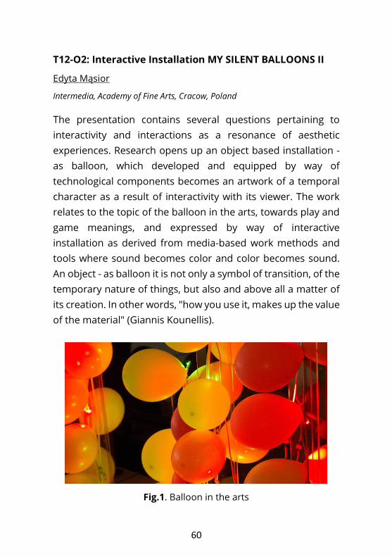
T12-O2: Interactive Installation MY SILENT BALLOONS II
Edyta Mąsior
Intermedia, Academy of Fine Arts, Cracow, Poland
The presentation contains several questions pertaining to interactivity and interactions as a resonance of aesthetic experiences. Research opens up an object based installation - as balloon, which developed and equipped by way of technological components becomes an artwork of a temporal character as a result of interactivity with its viewer. The work relates to the topic of the balloon in the arts, towards play and game meanings, and expressed by way of interactive installation as derived from media-based work methods and tools where sound becomes color and color becomes sound. An object - as balloon it is not only a symbol of transition, of the temporary nature of things, but also and above all a matter of its creation. In other words, "how you use it, makes up the value of the material" (Giannis Kounellis).
Fig.1. Balloon in the arts

61
Relation between a spectator – observer – player is an important part in reaching the interactivity as well as is showing how can movements be „heard” and sound be „coloured”? How is it possible to combine disciplines such as chemistry, physics and informatics and exploit them in medicine, robotics and art? How can we communicate with the environment through the detectors and sensors, such as light, motion, and others. In artistic research with technological connections and epistemological background, where philosophy (post-structuralist thought) meets history of art and aesthetic perception (radical constructivism) with the reflection in media theories (like classified by Marshall McLuhan, like understood by Friedrich Kittler), concentrates on translocation on new media, underlining a new sensorium (media interactions) towards haptic environment obtained by use of a sensor fields and brings up several questions according to context of technology in new media - anthropology is a knowledge or perspective? Are we being creative when we are publishing what we are observing?

62
T12-O3: The Moon Arts Project, nanotechnology, and contemporary art
Chris Robinson
Visual Art, University of South Carolina School of Visual Art & Design, Columbia, USA
The Moon Arts Project as part of the Google Lunar X Prize tags along on an ambitious competition to send a privately funded rover to the moon, travel 500 meters on the lunar surface, and send back high definition video. First prize is $20 million. Space X is the launch vehicle and Astrobotic, the robotics company constructing the rover, generously reserved payload space for a group of artists to send along some representation of humanity. The creative team is based in the Studio for Creative Enquiry at Carnegie Mellon University, with participants from all over the world, and the charge was to provide a meaningful artifact weighing no more than 6 ounces and fit in a cylinder about half the size of a soda can. In this small pentagonal structure will be four interrelated chambers – Earth, Metasphere, Moon, and Ether. Each of these four chambers will hold two sapphire disks, metal sculptures, microcapsules, and high resolution imagery on metal foil with a collection of images and objects raging from iconic nano-imagery to artificial blood, and deep space radio transmissions. While I recognize that there is some comedy about an ambitious, time consuming, very small project, carefully designed to stand up to the rigors of space and space flight, have an interpretable structure and communications logic, last indefinitely, though probably never be seen or read, we have taken it very seriously for several

63
years. The project has required the careful curatorial consideration and selection of subject matter – a miniature museum of life on earth, invention of new technologies, rare materials, and specialized applications, and, along with going to the moon, a curated exhibition will be shown at terrestrial museums in Paris and ten other European cities, among others. This presentation will provide some history, insight to the images, complexity and aspects of the idea and undertaking, space art, the Moon Museum – based in nanotechnology, participants, and what it all means.

64
Monday, September 12, 2016
09:00
Plenary Session
Hall 1: George Calugareanu Amphitheater
10:45 Coffee Break
11:15
Plenary Session
Hall 1: George Calugareanu Amphitheater
13:00 Lunch
15:00
Invited Lectures
Hall 4: Florin Stefanescu Goanga
17:15 Coffee Break
18:00 Invited Lectures
Hall 4: Florin Stefanescu Goanga

65
Plenary Session (PL)
Hall-1: George Calugareanu Amphitheater
PL10: Fabrication and investigation of photoinduced exciton-plasmon nanocomposites
N. Bityurin1, N. Ermolaev1, A. A. Smirnov1, A. Afanasiev1, S. Gusev2, D. Tatarskiy2
1Institute of Applied Physics, RAS, 603950, Nizhniy Novgorod, Russia 2Institute of Physics of Microstructures, RAS, 603950, Nizhniy Novgorod, Russia
UV irradiation of materials consisting of a polymer matrix that possesses precursors of different kinds can result in creation of nanoparticles within the irradiated domains. Such photoinduced nanocomposites are promising for photonics applications due to the strong alteration of their optical properties compared to initial nonirradiated materials. We report our results on the synthesis and investigation of plasmonic, excitonic and exciton-plasmonic photo-induced nanocomposites. Plasmonic nanocomposites contain metal nanoparticles of noble metals with a pronounced plasmon resonance. Excitonic nanocomposites possess semiconductor nanoclusters (quantum dots). We consider the CdS –Au pair because the luminescent band of CdS nanoparticles enters the plasmon resonance band of gold nanoparticles. The obtaining of such particles within the same composite materials is promising for the creation of media with exciton-plasmon resonance. We demonstrate that it is possible to choose appropriate precursor species to obtain the initially transparent polymethylmethacrylate (PMMA) films containing both types of these molecules either separately or together.

66
Proper irradiation of these materials by a light emitting diode (LED) operating at the wavelength of 365nm provides material alteration demonstrating light-induced optical absorption and photoluminescence properties typical for the corresponding nanoparticles. Thus, an exciton-plasmonic photoinduced nanocomposite is obtained. Optical absorption and luminescent spectroscopies as well as optical confocal and electronic microscopies are used to investigate optical properties and structure of the obtained materials. We show that the formation of photoinduced nanocomposites cannot be reduced either to pure photochemical or to pure photothermal effects. We discuss the opportunity to obtain correlated spatial distribution of plasmonic and excitonic particles in these materials in order to control their optical properties.

67
PL11: Composite materials with controlled properties from selfassembly of nanoparticles
Marco Lattuada
Adolphe Merkle Institute, University of Fribourg, Fribourg, Switzerland
Since the term ‘nanocomposites’ has been proposed for the first time by Theng in 1970, the field has grown in a mature and highly developed branch of material science. Numerous procedures for the preparation of nanocomposite materials have been investigated in order to generate materials with controlled features, which is still one of the great challenges in nanotechnology. The purpose of this work is to use the extended and large knowledge of self-assembly behavior of nanoparticles in aqueous dispersions and its dependence on interparticle interactions for the preparation of hybrid nanostructured composites. The nanocomposites have been obtained from mixed aqueous dispersions of soft poly(butyl acrylate/methyl methacrylate) copolymer particles (80 nm diameter) and filler particles. Two different filler particles have been utilized: hard silica nanoparticles (20 nm diameter), with various concentrations, and graphene oxide nanosheets. In order to investigate the specific role of the interparticles interaction on the final structure and mechanical properties of the materials, the nanocomposites have been synthetized following two different assembly strategies. The first strategy consists in mixing the two stable particle suspensions with same surface charge. The second strategy consists in inducing aggregation/gelation of the filler particles inside the matrix particle stable suspension. The excellent dispersion of the filler

68
particles in the polymer matrix achieved by this methods, the ability to control the microstructure of the composite material lead to excellent mechanical properties, which can be tuned by controlling the degree of association of the filler particles. The same procedure has been used to prepare composite materials reinforced with amyloid fibrils, which are less known but have similar structure to silk fibers and are much easier to prepare. Protein fibrils are self-assembled structures resulting from partial denaturation of certain proteins, and the resulting aggregation mediated by beta-sheets interactions. These structures are characterized by an extremely large aspect ratio, with a diameter that changes depending on the age of the fibrils, and on the degree of association of the different

69
PL12: Cross over between ferromagnetic and antiferromagnetic order in Fe itinerant-electron metamagnetism of the RFe2 compounds
L.V.B. Diop1,2, O. Isnard1,2, Z. Arnold3, J. Kastil3, D. Benea4, M. Amara1,2, J. Kamarad3
1Univ. Grenoble Alpes, Inst NEEL, F-38042 Grenoble, France 2CNRS, Inst NEEL, F-38042 Grenoble, France 3Institute of Physics AS CR v.v.i., Na Slovance 2, 182 21 Prague 8, Czech Republic 4 Faculty of Physics 400084 Cluj-Napoca, Romania, Universitatea Babes-Bolyai, 400084 Cluj-Napoca, Romania
The RFe2 compounds are well known for their high performances as functional materials for magnetostrictive applications in sensors and actuators (R=Tb or Dy) [1,2]. Remarkable magnetic properties arise from the Fe sublattice when non magnetic R elements are used. This is consequently also a large playground from fundamental point of view. The magnetic order of Fe can change dramatically from ferromagnetic (FM) to antiferromagnetic (AFM) depending upon the nature of R element or the application of pressure. We present a detailed investigation of the unusual magnetic behavior of RFe2 intermetallic compounds at the cross over between these two types of order. In particular the existence of itinerant-electron metamagnetic transition in Hf1-xTaxFe2 compounds is described. Magnetic as well as magnetocaloric properties are presented together with transport and magnetotransport properties. A large sensitivity of the magnetic behavior to the volume effects is observed and analysed combining macroscopic (i.e.volume magnetostriction) and microscopic (neutron diffraction) techniques. The extreme

70
sensitivity of Fe magnetism in these compounds is discussed and illustrated by investigation of the magnetic phase diagram versus concentration, temperature (2 to 800K), pressure (up to 1.1GPa) and magnetic field (up to 10T).
[1] L.V.B. Diop, M. Amara, O. Isnard, J. Phys. Condens. Matter 25 (2013) 416007. [2] L.V.B. Diop, O. Isnard, E. Suard, D. Benea, Solid State Commun. 229 (2016) 16.

71
PL13: Chiral magnetic domain walls and skyrmions in Pt/Co/Oxide trilayers with perpendicular magnetization
Jan Vogel 1,2, Olivier Boulle2, Liliana Buda-Prejbeanu2, Stanislas Rohart3, André Thiaville3, Stefania Pizzini1
1Institut Néel, Centre National de la RechercheScientifique/ Université Grenoble Alpes, Grenoble, France 2Spintec, UGA/CEA/CNRS, Grenoble, France 3Laboratoire de Physique des Solides, CNRS/Université Paris-Sud, Orsay, France
Ultrathin magnetic films with structural inversion asymmetry have been extensively studied in the last 5 years, since it was shown that domain walls could be moved efficiently with current pulses in this type of systems [1]. Several experimental and theoretical studies revealed that this and related phenomena could be explained by the inversion asymmetry of the stack and the presence of the heavy metal (Pt) underlayer, leading to several effects induced directly or indirectly by the spin-orbit interaction, like Spin Hall effect, Rashba effect and Dzyaloshinskii-Moriya interaction. The Dzyaloshinskii-Moriya interaction (DMI) is an anti-symmetric exchange interaction that favors orthogonal alignment of neighboring spin. It can only exist in the absence of structural inversion symmetry, like in thin magnetic films with two different interfaces. In these films, this interaction can lead to chiral magnetic domain walls and other chiral spin structures, like skyrmions. We have used Magneto-optic Kerr microscopy to study the nucleation [2] and propagation [3] dynamics of such chiral domain walls in Pt/Co/AlOx and Pt/Co/GdOx films and microstructures with 0.6-1 nm of Co. The dependence of the nucleation field and the
72
domain wall propagation speed on the strength of an in-plane magnetic field can be used to determine experimentally the strength of the DMI. The strong value of the DMI that we observed allows for vortex-like chiral spin textures, called skyrmions, to be stabilized in such thin films. We indeed directly observed skyrmions, at room temperature and in zero magnetic field, using high-resolution magnetic microscopy. We also addressed the size and stability as a function of applied magnetic field, showing that they persist up to magnetic fields well above the coercive field of the films thanks to their topological stability. [1] I. M. Miron et al., Nat. Mater. 10, 419 (2011). [2] S. Pizzini et al., Phys. Rev. Lett.113, 047203 (2014). [3] M. Vanatka et al., J. Phys. Cond. Mat. 27, 326002 (2015).

73
PL14: Quantum criticality in a spin liquid compound
Martin Mansson
Dep. of Materials and Nano Physics, KTH Royal Institute of Technology, Stockholm, Sweden
Quantum phase transitions have been in the centre of attention for scientists world-wide to understand the universality of quantum critical behaviour in many-body systems. Gapped Heisenberg spin-½ systems have the potential to exhibit quantum critical phenomena in their excitation spectra as a function of e.g. magnetic field and pressure. In such compounds, tuning of the spin gap exercises a control of the ground state and enables the study of novel fundamental many-body phenomena. One example of such system is the organometallic quantum antiferromagnet [C4H12N2]Cu2Cl6 (PHCC). PHCC features Cu2+ spins coupled through a complex network of overlapping orbitals, forming slightly skewed anisotropic S=½ ladders in the ac-plane with frustrated Cu–Cl–Cl–Cu super-exchange interactions. Previous inelastic neutron scattering (INS) data show a spectral gap Δ≈1 meV and nearly isotropic 2D dispersion in the (h,0,l) plane. In the absence of a magnetic field/pressure, only short-range dynamic spin correlations typical of a liquid exist and the spin gap prevents any long-range magnetic order down to T=0 K. This makes PHCC an ideal compound for studying field/pressure induced magnetic order as well as tuning of exchange interactions through random bond disorder by chemically substituting some Cl for Br. Our recent INS and bulk experiments [1-3] show that magnetic order is induced by a magnetic field Hc = 7.6 T in
74
pure PHCC at T = 50 mK. With increasing Br substitution the critical field increases as the super-exchange bond angles i.e. AF bond strengths, are locally modified. This is also evident in the INS data that show an increase of the spin gap for H = 0 with increasing Br substitution. A ‘cleaner’ and more direct alternative to chemical pressure is to apply an external hydrostatic pressure. From our muon spin rotation (μSR) experiments; we find that magnetic order can be induced by rather moderate hydrostatic pressures [4]. We find a first transition at Pc1 = 4 kbar, a quantum critical point (QCP) separating the gapped spin liquid from an incommensurate ordered state. A second transition is also found, at Pc2 = 14 kbar, which likely is a commensuration transition, accompanied by a Lifshitz point (LiP) at a finite T.
[1] D. Hüvonen, M. Månsson et al. PRB 85, 100410(R) (2012). [2] D. Hüvonen, M. Månsson et al. PRB 86, 214408 (2012). [3] D. Hüvonen et al. PRB 88, 094402 (2013). [4] M. Thede, M. Månsson et al., PRL 112, 087204 (2014).

75
PL15: A new measurement method to study diseases of human bones
Francesco Lamonaca1, Monica Vasile2, Domenico Grimaldi3, Alfonso Nastro4 1Department of Engineering, University of Sannio, Benevento, Italy 2Medical School, Ovidius University, Costanta, Romania 3Computer Science, Electronic, Modelling and System Science, University of Calabria, Arcavacata di Rende, Italy 4Chemistry and Chemical Technologies, University of Calabria, Arcavacata di Rende, Italy
The diagnosis of bone diseases is mainly obtained by means of the symptoms detected by a doctor during an examination followed by X-Ray image analysis. As a consequence, the early detection of bone diseases mainly depends on the level of pain tolerance of the patient and the experience and expertise of the clinicians. Aim of the research is to furnish a new objective methodology based on Thermal Analysis (TA) for the diagnosis of bone pathologies. The main idea is that a disease alters the mechanisms of dissolution and precipitation of the hydroxyapatite forming the bone through collagen, and thus the ratio between organic and inorganic bone components. These different ratio values, with respect to the ones of healthy bone, can be detected by TA. TA is proposed because: (i) it does not expose patients and clinicians to the potential risks of radiation; (ii) it can be performed on few milligrams of bone (at least 20 mg), (iii) owing the reduced quantity, the bone sample can be draw by means of a needle in ambulatory under local anesthesia, or directly in the surgical room; (iv) thermal analysis can be performed in less than 15–20 min; and (v) thermal analysis can be performed directly in the surgical room.

76
Moreover, since thermal analysis is a well-known and routine measurement technique for the study of ceramics and polymeric materials, the measurement instrument is easily available commercially. In the research TA was successful used for the detection of Hallux Valgus [1], Gonarthrosis [2], Osteosarcoma Tumors [3]. Experimental results were performed (i) to assess the suitability of the pointed out characterization method, and (ii) to allow the definition of parameters to evaluate bone diseases. For the above reported reasons, the proposed measurement method can be considered a promising objective tool to support the diagnosis of bone diseases, and then to increase the probability of patient survival and quality of life, which nowadays mainly depends on the ability and experience of clinicians.
[1] Lamonaca et.al, Measurement, vol.57, 2014, pp.97-101. [2] Lamonaca et.al, International Journal of Biology and Biomedical Engineering, Vol.8, 2014, pp. 184-190. [3] Lamonaca et.al, Measurement, vol.92, 2016, pp.89–95.

77
Invited Lectures (IL)
Hall 4: Florin Stefanescu Goanga Hall
IL12: Smartphone: a portable and flexible health parameters measurement platform
Francesco Lamonaca1, Domenico Luca Carnì2, Maria Riccio1, Domenico Grimaldi2, Alfonso Nastro3, Vitaliano Spagnuolo4
1Dept. of Engineering, University of Sannio, Benevento, Italy 2Computer Science, Electronic, Modelling and System Science, University of Calabria, Arcavacata di Rende, Italy 3Chemistry and Chemical Technologies, University of Calabria, Arcavacata di Rende, Italy 4Clinical and Therapeutic Unit of Arterial Hypertension – Unit of Internal Medicine, AO of Cosenza, Cosenza, Italy
The large diffusion of smartphones equipped with different sensors has stimulated the development of applications for health parameters monitoring [1]. Aim of the abstract is to provide an overview of the most significant health-care applications. Interest is focused on the use of (i) 3D accelerometer for actimetric, body posture and falls monitoring, (ii) camera for evaluating cardiovascular system parameters, blood oxygen saturation (SpO2%), and eye pathologies, and (iii) microphone for recognizing respiratory system diseases. A comparison of these applications to traditional medical devices is discussed to highlight strong and weak points. As a consequence, it will be presented data processing methods designed to overcome the weak points deriving from the use of general purpose sensors not optimized for health monitoring. On this line, major weak points are in the

78
use of the camera. Hearth rate [2], Blood pressure [3,4] and oximetry [5,6] are evaluated by analyzing the photopletysmogram (PPG), the volumetric measurement of blood in body peripheries. The change in volume is detected by illuminating the skin and then measuring the amount of light either transmitted or reflected. To this aim, commercial pulse oximeter uses two Light Emitting Diode (LED), in the range of red and infrared, and a photodiode. Two PPGs are obtained, referred to red and infrared light. Because oxy and deoxyhemoglobin adsorb red and infrared light in different way, the two PPGs allows the SpO2% evaluation. The smartphone uses a wide spectrum LED. The SpO2% is evaluated from the PPGRed and PPGGreen signals evaluated for the red and green color channels of the camera. Heart Rate and Blood pressure are evaluated from PPGRed. The external light affects in different manner the smartphone’s camera, depending on the model and manufacture. Kind of skin, non-perfect positioning or movements of the finger on the camera, introduce artefact on the reconstructed PPGRed and PPGGreen misstating the health parameters evaluation. To overcome these weak points, recent literature has proposed a proper method for setting-up the parameters compensating the effects of the environmental light and detect PPGs artefacts.
[1] Lamonaca et.al, Measurement, 73, 28, 2015, p82-94. [2] Lamonaca et.al, MeMeA 2012, p234-237. [3] Polimeni, et.al, MeMeA 2014, p433-438. [4] Lamonaca et.al, IDAACS 2013, p408-412. [5] Lamonaca et.al, MeMeA 2015, p359-363. [6] Lamonaca et.al, MeMeA 2016, p430-435.

79
IL-13: Some aspects of laser nano-structuring of polymers
Nikita Bityurin
Institute of Applied Physics RAS, 603950, Nizhniy Novgorod, Russia
This lecture considers several approaches to laser nano-structuring of materials based mainly on experiments with polymers. Laser irradiation of polymer surfaces results in the formation of either ablation craters or bumps. The mechanisms of creation of such structures at nano-scales are discussed. Attention is primarily paid to laser swelling, the least studied phenomenon that is promising for the surface nano-structuring of polymers and glasses. The relaxation mechanism of laser swelling of polymers is described. Simultaneous surface nano-structuring on large areas can be performed using either colloidal nano-particle lens arrays deposited on the material surface or interference lithography. In the former case, the colloidal particles serve as near-field lenses for obtaining features with sizes smaller than the laser wavelength. Important features of such kind of nano-structuring are studied. Examples of the nano-structures produced by this technique are demonstrated. Laser nano-structuring within the bulk of the material can be achieved by a tightly focused laser beam using both nonlinear light absorption and a strongly nonlinear material response. In more detail, such kind of 3D nano-structuring is considered in terms of nano-polymerization. Nano-structured materials can also be produced even by laser exposure without tight focusing if irradiation leads to the development of an instability resulting in the formation of nano-clusters or nano-inhomogeneities in
80
the initially homogeneous medium. We present the results on the synthesis and examination of plasmonic, excitonic, and exciton-plasmonic photo-induced nano-composites. Plasmonic nanocomposites contain metal nanoparticles of noble metals with a pronounced plasmon resonance. Excitonic nano-composites have semiconductor nanoclusters (quantum dots). We discuss the possibility of obtaining a correlated spatial distribution of plasmonic and excitonic particles in these materials in order to control their optical properties.

81
IL-14: Neutron scattering as a research tool for studying magnetism
Ovidiu Garlea
Quantum Condensed Matter Division, Oak Ridge National Laboratory, Oak Ridge, United States
Sustained advances in experimental and computational methods over the past few decades have greatly increased the sensitivity and range of applications of neutron scattering. Nowadays, neutron scattering is recognized as the most powerful technique for detailed studies of static and dynamic magnetic properties in complex magnetic materials. The energies of thermal and cold neutrons are of the same order of magnitude with microscopic excitations in condensed matter, and their wavelengths are comparable to the intermolecular distances. The objective of this lecture is to introduce audience to the current state of neutron scattering research, with direct applications to a broad range of magnetism problems. An overview of the instrumentation and sample environments available at the Spallation Neutron Source and High Flux Isotope Reactor at the Oak Ridge National Laboratory will be provided.
82
IL15: Nanospectroscopy: enhancing the signals and the detection limit of very tiny objects
Dietrich RT Zahn
Semiconductor Physics, Technische Universität Chemnitz, D-09107 Chemnitz, Germany
The dimensions of structures of interest in e.g. electronic devices are nowadays in the nanometre range. A typical example is a carbon nanotube (CNT) field effect transistor (FET) where ideally a single CNT forms the channel or an organic FET where the thickness of the active layer is only a nanometre or so. Such dimensions or in other words low amounts of material impose challenges on characterisation techniques such as Raman spectroscopy which can provide an enormous amount of useful information but suffers at the same time from weak scattering cross-sections. There are, however, ways of overcoming the weak cross-sections by utilising enhancement mechanisms. Some of those will be discussed in this contribution. For this purpose, examples of semiconductor quantum dots and ultra-thin films of organic semiconducting molecules will be employed. The best known and most used enhancement mechanism in Raman spectroscopy is, of course, the resonance enhancement which takes place when the excitation used coincides in energy with real electronic transitions in the sample probed. Moreover, resonance enhancement is soften used together with other enhancement mechanisms. One of those is interference enhanced Raman scattering (IERS) where a dielectric layer beneath the material under study results in an increased signal when its optical

83
thickness fulfils destructive interference condictions. This can, for instance, be beneficial for the investigation of FET structures whith a gate dielectric layer. The most prominent enhancement mechanism nowadays is surface enhanced Raman scattering (SERS). Here several examples will be provided how SERS can be realised from the formation of in situ prepared but rather undefined metal clusters in a microfluidic channel for the detection of pollutants in water to well-defined metal nanocluster prepared by electron beam lithography. Unexpectedly high SERS enhancement can be achieved when combining well-ordered metal nanoclusters with photonic crystals. Finally tip enhanced Raman scattering (TERS) which allows achieving lateral resolution in the naometre range will be introduced.
84
IL-16: Strain engineering and Raman spectroscopy: from silicon to multiferroics
Cameliu Himcinschi
Institute of Theoretical Physics, Technische Universität Bergakademie Freiberg, Fraiberg, Germany
Varying the strain in materials offers a useful parameter for tuning various material properties. In silicon, by example, induced strain provides enhanced carrier mobility compared to the unstrained counterparts. On the other hand, in ferroelectric or multiferroic materials one can change the electric polarisation by changing the strain and thereby enhance or reduce the ferroelectricity. Raman spectroscopy is a viable, nondestructive, and sensitive method which allows to study the strain in such material systems based on the exploration of the frequency range of the lattice vibrations. In this lecture several examples will be discussed where Raman spectroscopy was applied to quantitatively determine the strain and furthermore to investigate the coupling phenomena induced by epitaxially, mechanically or piezoeletrically applied strain.

85
Tuesday, September 13, 2016
09:00 Plenary Session
Hall-1: George Calugareanu Amphitheater
10:45 Coffee Break
11:40
Invited Lectures
Hall 4: Florin Stefanescu Goanga Hall
13:10 Lunch
15:00
Invited Lectures
Hall 4: Florin Stefanescu Goanga Hall
17:15 Coffee Break
18:00
Invited Lectures
Hall 4: Florin Stefanescu Goanga Hall
19:30 Conference Dinner

86
Plenary Session
Hall 1: George Calugareanu Amphitheater
PL16: Nanopatterning of surfaces with nanosphere lithography, block-copolymer lithography and combinations of both
Katharina Brassat1,2, Christoph Brodehl1,2, Jörg K. N. Lindner1,2
1Department of Physics, Paderborn University, 33098 Paderborn, Germany 2CeOPP, Center for Optoelectronics and Photonics, Paderborn University, 33098 Paderborn, Germany
Nanosphere lithography (NSL) is a well-established technique to form regular surface patterns with periodicities in the range of several hundred nanometers where self-arranged colloidal spheres act as shadow mask to modify the substrate at the free interstices between the spheres. Recently, NSL technique was used to direct the growth of semiconductor nanowires, to arrange proteins on a surface and to create novel plasmonic devices, mostly by combining NSL with physical vapor deposition PVD, chemical vapor deposition CVD and/or reactive ion etching RIE. In order to achieve patterns which are 1-2 orders of magnitude smaller than the ones created by NSL, block copolymer (BCP) lithography can be employed. This is an emerging self-organization technique in which the phase separation of BCP molecules is exploited to generate regular surface patterns the periodicity of which is governed by the length of polymer chains. The drawback of BCP lithography so far is the small length scale over which the periodicity is maintained. Therefore, pre-patterning of the substrate prior to

87
the application of BCP lithography is required in order to direct the self-assembly of BCPs. It will be demonstrated that the combination of NSL and BCP lithography is a promising low-cost attempt to form well-ordered surface patterns on wafer-scale surfaces with motive sizes in the sub-20 nm range.
88
PL17: Non-linear phenomena in nano-scale oxide layers and multilayer structures
Peter Petrov
Faculty of Engineering, Department of Materials, Imperial College London, London, United Kingdom
Nano-scale oxide layers are a promising solution for establishing next-generation elements, their impact being realised through their truly nanoscale dimensions, their capacity to store multiple bits of information per element with minimal energy required and most recently through their ability to guide plasmonic signal. This presentation will present our recent achievements in developing of ultra-thin (less than 10nm thick) oxide layers, and modulated superlattice samples consisted of continuous well defined 1nm SrTiO3 and 4nm BaTiO3 layers with atomically sharp interfaces, using RHEED assisted pulsed laser deposition and controlled oxidation. The results of thin films structural characterisation and electrical measurements are compared with the theoretical predictions. The applicability of these films as gate dielectrics, RF tuneable devices and next-generation memory elements will also be discussed. The process of oxygen annealing of single layer CVD graphene transferred on various substrates was investigated and the growth of SrTiO3 epitaxial thin films on graphene si described. The proposed mechanism is supported by first principles simulation and structural characterisation results. The possibility to develop a new class functional oxide/graphene based microwave devices will also be discussed.

89
PL18: All-optical helicity-dependent switching in magnetic thin films and devices
Michel Hehn1, Mohammed El Hadri1, Charles Henri Lambert1, Gregory Malinowski1, Mathias Gottwald1, Martin Aeschlimann3, Eric Fullerton2, Stéphane Mangin1 1P2M, Institut Jean Lamour, VANDOEUVRE LES NANCY, France 2Center for Magnetic Recording Research, University of California San Diego, La Jolla, USA 3Department of Physics and Research Center OPTIMAS, University of Kaiserslautern, Kaiserslautern, Germany
Since Beaurepaire et al’s observation of ultrafast demagnetization in Ni films arising from a pulsed laser excitation [1], there has been a drive to understand the interaction between the ultrashort laser pulses and magnetization. These studies led to the discovery of the “All-Optical Switching” of magnetization in a ferromagnetic film alloy of GdFeCo using femtosecond laser pulses [2]. All Optical switching leads to a deterministic magnetization reversal of the material with no external magnetic field; the direction of the resulting magnetization is given by the right or left circular polarization of the light. The manipulation of magnetization through laser beam had long been restricted to one material. We will show that AOS is a more general phenomenon for a variety of ferrimagnetic materials; including alloys, multilayers and heterostructures, as well as rare earth free synthetic ferrimagneticheterostructures [3]. Furthermore, we have observed the same phenomenon in single ferromagnetic films, thus paving the way for an integration of the all-optical writing in storage industries. It is within that context that we are studying the effect of femtosecond laser pulses on magneto-

90
resistive systems with perpendicular magnetic anisotropy, with the aim of identifying the magnetization orientation through an electrical signal. We measure the all-optical switching in Pt/Co/Pt and Tb27Co73 based Hall crosses via the anomalous Hall effect. This new way of probing the all-optical switching enables a statistical quantification of the switching ratio for different laser parameters. We will present results on hall crosses for both ferrimagnetic and ferromagnetic materials.
[1] E. Beaurepaire et al, Phys. Rev. Lett. 76 (22) (1996) 4250-4253. [2] C. D. Stanciu et al, Phys. Rev. Lett.99 (2007) 047601. [3] A. Kirilyuk, et al, Rev. Mod. Phys. 82 (2010) 2731 - 2784.

91
Invited Lectures (IL)
Hall 4: Florin Stefanescu Goanga Hall
IL-17: Quantum superconducting circuits
Ioan Pop
Physikalisches Institut, KIT, Karlsruhe, Germany
Following the first demonstration of a coherent superconducting circuit, almost 20 years ago, the field of quantum information processing using superconducting quantum bits has witnessed an exponential growth. The current performances suggest that within a horizon of a few years, superconducting quantum machines could outperform even the best classical machines for a few types of particularly hard tasks. During the class I will introduce the basic elements of superconducting micro-electronics, and I will show how they can be used to construct a quantum bit.

92
IL18: New magnetic properties and applications of thin magnetic films
Jan Vogel
Institut Néel, CNRS and Université Grenoble Alpes, Grenoble, France
Magnetic materials are used for many different applications, like car motors, windmills, transformers, oscillators and magnetic recording. In this lecture, I will discuss some issues and developments concerning this last application. I will introduce some basics of the magnetism of ultrathin films and nanostructures. I will then concentrate on recent developments concerning thin magnetic films having their magnetization direction perpendicular to the film surface. Trilayer stacks where a thin magnetic film is sandwiched between a heavy metal like Pt and a lighter non-magnetic metal or oxide can show properties which are of particular interest for magnetic recording. In narrow magnetic strips made of these stacks, magnetic domain walls can propagate at high speeds when short current pulses are applied. Small current pulses can also lead to fast switching (<1ns) of the magnetization direction of nanostructures made of these stacks. I will discuss the physical origin of these properties, which are related both to the lack of structural inversion symmetry of such stacks and to the strong spin-orbit coupling in the heavy metal layer.

93
IL19: Probing the electronic band structure of solids by angle-resolved photoelectron spectroscopy (ARPES)
Yasmine Sassa
Department of Physics and Astronomy, Uppsala University, Ångström Laboratory, Uppsala, Sweden
Angle-resolved photoelectron spectroscopy (ARPES) is the most powerful method for probing the electronic structure of solids. By irradiating the sample with a monochromatic beam, the material emits photoelectrons that carry both the energy and momentum information of the electrons inside the solid. Particularly important are the high energy and momentum resolution of the technique that give access to electronic excitations, and allow the study of the electronic, magnetic and chemical properties of complex materials. Furthermore, the ARPES technique has turned the abstractions of Landau quasiparticles and the electronic Fermi sea into reality! In this lecture I will introduce the principle of photoemission and present some illustrative experimental results ranging from lightly to highly correlated systems. I will show how ARPES can probe the momentum-dependent electronic structure of solids providing detailed information on band dispersion and Fermi surface as well as on the strength and nature of many-body correlations.
[1] Stephan Huefner, “Photoelectron Spectroscopy, Principles and Applications”, Springer. [2] Stephan Huefner, “Very High Resolution Photoelectron Spectroscopy”, Lect. Notes Phys. 715 (Springer, Berlin Heidelberg 2007).

94
IL20: Alternative materials for plasmonic applications
Peter Petrov
Faculty of Engineering, Department of Materials, Imperial College London, London, United Kingdom
Several new plasmonic materials have recently been introduced in order to achieve better temperature stability than conventional plasmonic metals and control field localization with a choice of plasma frequencies in a wide spectral range. Here, epitaxial SrRuO3 TiN and TiON thin films with low surface roughness are studied. It is demonstrated that SrRuO3 thin films exhibit plasmonic behavior in the near-infrared spectral range with the plasma frequency in 3.16 – 3.86 eV range and epsilon-near-zero wavelength in 1.11 – 1.47 μm range that could be controlled by the deposition conditions.

95
IL21: High-fluence laser ablation of advanced materials: space- and time-resolved optical and electrical characterization methods
Cristian Focsa
Laboratoire de Physique des Lasers, Atomes et Molécule, Centre d’Etudes et de Recherches Lasers et Applicationss, Université Lille 1 Sciences et Technologies, 59655 Villeneuve d’Ascq cedex, France
The behavior of various materials under intense laser irradiation is a topic of high current interest, both for its fundamental aspects and for its significant importance in solving new technological challenges. As a consequence of the intense pulsed irradiation, a luminous transient plasma is generated. A complete characterization of this non-stationary phenomenon in terms of dynamics, chemical and electrical composition, energetic or possible interaction with surrounding environment, can find great applications in, e.g. technological approaches like PLDor analytical methods like LIBS. This lecture will present an overview of several optical (space- and time-resolved emission spectroscopy, fast ICCD imaging, absorption spectroscopy, laser induced fluorescence) and electrical (Langmuir probes, mass spectrometry) methods of investigation. The fundamental issues will be complemented with concrete examples from our research group or from the literature. Results obtained on various classes of materials, from the simplest ones to more complex will be briefly described. Some hints will also be given on theoretical efforts developed to account for the experimental findings.

96
IL22: Physicochemical properties of nanoparticles suspensions
Marco Lattuada
Adolphe Merkle Institute, University of Fribourg, Fribourg, Switzerland
Nanoparticles are the key elements of the booming nanotechnology. Very often nanoparticles are used in suspensions, and the properties of such suspensions are vital for the applications of nanoparticles in different fields. This lecture is devoted to learning and understanding the most important physico-chemical properties of nanoparticles suspensions. A particular focus will be dedicated to their colloidal stability and on how stability affects the fate and behavior of suspensions. The experimental characterization of suspensions will be discussed. Several examples of the consequences of colloidal stability on the utilization of the nanoparticles will be highlighted.
97
IL23: Physical processes at the metal/ semiconductor and semiconductor/semiconductor interfaces
Stefan Antohe1,2
1Physics, University of Bucharest, Magurele, Romania 2Physics, Academy of Romanian Scientists, Bucharest, ROMANIA
The M/S contact is an important part of the electronic and optoelectronic devices, either as an active element or as a charge carrier collector. The M/S interface processes and the diffusion potential value at the M/S contact depend on two factors: a) The difference between the metal work function )M and the semiconductor work function )S; b) The presence of the surface states in the semiconductor. Taking into account these factors the classification of the M/S interfaces, prepared with different work function deposited on n- or p-type semiconductors, will be presented. Elements of depletion layer theory at M/S interface together with the models for the transport charge carrier through them will be detailed discussed too. In the second part of this presentation, the properties of organic-on-inorganic (OI) semiconductor contact barrier diodes, where the 3, 4, 9, 10 perylenetetracarboxylic diimide (PTCDI) and the copper phthalocyanine (CuPc) serve as the organic thin film, are discussed. The results presented can be fully understood in terms of the thermionic emission-space-charge limited (TE-SCL) current model introduced for OI structures with prototypical aromatic compound; 3, 4, 9, 10 perylenetetracarboxylic dianhydride (PTCDA) vapor-deposited onto n- and p-Si substrates. Also, under moderate and high reverse bias voltages the results obtained can be understood in

98
terms of the organic-on-inorganic heterojunction (OI-HJ) model. Comparisons between diode performances and theory are made. The resulting diodes are superior with respect to conventional Schottky diodes due to enhanced contact barriers and reduced edge effects. The low-frequency conductance and capacitance characteristics can be used to obtain information about the magnitude and energy distribution of surface states in inorganic semiconductor band gap. Also, the carrier concentration profile of the substrate can be convenient obtained. This technique is applied to 0I diodes using thin films of copper phtalocyanine (CuPc) and 3, 4, 9, 10 perylene-tetracarboxylic diimide (PTCDI) vapour-deposited onto p-Si substrates. Keywords: Metal/Semiconductor contact, Schottky diodes, Organic/Inorganic diodes, SOISAS.
[1] S. Antohe, Organic materials and Electronic Devices, Editing House of University of Bucharest, Bucharest 1996. [2] S. M. Sze, Physics of Semiconductor Devices, Wiley Interscience, New York (1969).

99
Wednesday, September 14, 2016
09:00
Plenary Session
Hall 1: George Calugareanu Amphitheater
10:10
Coffee Break and Poster Session IV
Foyer
12:10
Plenary Session
Hall 1: George Calugareanu Amphitheater
13:20
Awards and Closing Ceremony
Hall 1: George Calugareanu Amphitheater
14:00 Lunch

100
Plenary Session (PL)
Hall 1: George Calugareanu amphitheater
PL19: SiGe nanostructures roadmap
Antoine Ronda, Antoine, Thomas David, Luc Favre, Marco Abbarchi, Isabelle Berbezier
IM2NP, CNRS, Aix-Marseille University, Marseille, F-13397, France
While conventional silicon-based electronics has experienced rapid and steady growth, thanks to the progressive miniaturization of its basic component, the transistor, this trend cannot continue indefinitely. At the moment, the actual bottleneck for further scaling trends is that, even using bulk materials, the functionality of electronic devices is essentially governed by what occurs at the interface of the semiconductor. Industry has already moved to thin film channel devices with the production of the FinFET, in which a thin film silicon channel is placed vertically. An attractive option for entering the <11 nm nodes is the ultrathin body silicon on insulator (UTB SOI) design that consists of a thin film Si channel placed horizontally. This architecture benefits for low power operation but its scaling down to the <5nm lower nodes will be inherently hindered by both the imperfect interface and non-uniformity of such a very thin film and by quantum confinement effects which increase the effective bandgap. Radical change of paradigm has already been made with the emergence of new technologies based on nanowires, quantum dots and more recently 2D materials, that could allow the

101
ultimate thickness scaling required beyond the 7-5 nm technology node. Some examples of realization of new nanoobjects will be shown. In particular, the fabrication of flat, two-dimensional silicon (germanium) sheets showing a honey-comb lattice that matches that of silicene (germanene) by depositing submonolayers of Si(Ge) on graphite at room temperature and subsequent annealing to 350 °C. Scanning tunneling microscopy shows that the 2D layers have a small buckling with no atomic reconstruction and does not give any hints for alloy formation and hybridization with the substrate. The band structure calculations confirm that the Dirac cone of free-standing Si and Ge layers is preserved when they are supported on graphite. The growth process can easily be scaled-up on wafer size graphene substrate and opens promising routes for fabricating new generation of functional electronic devices based on silicene and germanene.

102
PL20: Untangling electrostatic and strain effects on the polarization of ferroelectric superlattices
E. Khestanova1, N. Dix1, I. Fina1, M. Scigaj1, J. M. Rebled1,2, C. Magén3, S. Estradé2, F. Peiró2, G. Herranz1, J. Fontcuberta1, F. Sánchez1 1MULFOX, Institut de Ciència de Materials de Barcelona (ICMAB-CSIC)), Bellaterra, Spain 2Electronics, University of Barcelona, Barcelona, Spain 3Laboratorio de Microscopías Avanzadas, Instituto de Nanociencia de Aragón (INA), Zaragoza, Spain
The polarization of ferroelectric superlattices is determined by both electrical boundary conditions at the ferroelectric-paraelectric interfaces and lattice strain. The combined influence of both factors offers new opportunities to tune ferroelectricity. However, the experimental investigation of their individual impact has been elusive because of their complex interplay. Here, we present a simple growth strategy that has permitted to disentangle both contributions by an independent control of strain in symmetric BaTiO3/SrTiO3 superlattices. It is found that fully strained short period superlattices display a large polarization whereas a pronounced reduction is observed for longer multilayer periods. This observation indicates that the electrostatic boundary mainly governs the ferroelectric properties of the multilayers whereas the effects of strain are relatively minor.

103
PAMS-2 Poster Session (part of Poster Session IV)
PAMS-P1: Dual-pulsed laser induced non-linear thermal effects
Alexandru Cocean, Silviu Gurlui, Felicia Iacomi
Faculty of Physics, Alexandru Ioan Cuza University of Iasi, Romania
In this paper we report on the preliminary investigations on the thermal effects behavior upon the ultrathin silver layer deposited on borosilicate substrate and irradiated with successive dual-pulsed lasers, and using COMSOL - multiphysics simulation software. The aim of the simulation is to study the temperature profiles behavior on surface and in volume of the irradiated target. Space time profiles of the temperature have been studied taking into account various experimental conditions: laser wavelength, pulse width, repetition rate and the delay time between the pulses. The laser irradiating effect based on Beer-Lambert law and thermal diffusion governed by the heat-transfer equation have been also considered in this study. The nonlinearity of the heating mechanism due to the Gaussian intensity distribution of the laser beams reflected in the nonlinear temperature variation will be exemplified and explained based on both Heating Transfer Module of COMSOL and additional data inserted in COMSOL as parameters, functions, variables.
[1] B.C. Widom, P. K. Diwakar, D.W. Hahn, Elsevier, Spectrochimica Acta Part B 61 (2006) 788 -796.

104
PAMS-P2: Composite materials based on Bi-Fe nanoparticles / Carbon Xerogel with environmental analytical applications
Mihai Rusu1, Carmen Ioana Fort2, Adriana Vulpoi1, Virginia Danciu2, Liviu Cosmin Cotet2, Lucian Baia1
1Faculty of Physics & Institute of Interdisciplinary Research in Bio-Nano-Sciences, “Babes-Bolyai” University, Cluj-Napoca, Romania 2Faculty of Chemistry & Chemical Engineering, “Babes-Bolyai” University, Cluj-Napoca, Romania
A new nanoporous composite based on C, Bi and Fe was investigated as a promising material for environmental applications. The multifunctional features of the obtained material are due to the combined characteristics of the three components: (1) C xerogels are adsorbant materials with tunable nanoporous structure, (2) Bi possess the ability to form fusible alloys with heavy metals and are used for heavy metal ion detection[1] (Pb(II), Cd(II), etc.) and (3) Fe enhances the electric and magnetic properties of the material and acts as catalyst for both the formation of graphene like carbon structures and analyte detection[2]. The nanoporous composite monoliths were obtained through a modified sol-gel synthesis. Resorcinol and formaldehyde were used to obtain a precursor organic gel, while Bi and Fe salts (Bi(NO3)3·5H2O and/or Fe(OAc)2) were added as co-synthesis functional agents. Afterwards, the gel was dried in ambient conditions and pyrolized in N2 atmosphere in order to carbonize the polymeric support and to obtain metal nanoparticles.

105
In order to assess the morphological and structural properties, the composites were characterized via X-ray diffraction (XRD), scanning electron microscopy (SEM), energy dispersive X-ray spectroscopy (EDX), transmission electron microscopy (TEM) and N2 adsorption/desorption method. The electrochemical behavior of the obtained modified electrodes and their ability to detect H2O2 and heavy metals (Pb(II)) has been investigated. The kinetic and analytical parameters of the investigated modified electrodes recommend them as stable, sensitive and reproducible sensors for H2O2 and heavy metals detection.
Acknowledgements This work was supported by a grant of the Romanian National Authority for Scientific Research and Innovation, CNCS – UEFISCDI, project number PN-II- RU-TE- 2014-4- 1194.
[1] C.I. Fort, L.C. Cotet, A. Vulpoi, G.L. Turdean, V. Danciu, L. Baia, I.C. Popescu, SENSOR ACTUAT B-CHEM 220 (2015) 712-719. [2] C.I. Fort, L.C. Cotet, V. Danciu, G.L. Turdean, I.C. Popescu, MATER CHEM PHYS 138 (2013) 893-898.
PAMS-P3: Development of fabrication technology of all solid-state planar supercapacitor with electrodes based on CNT-Nickel Oxide composite
Egor Lebedev1,2, Ilya Gavrilin1, Alexey Alexeev1, Artem Sysa1,2, Evgeny Kitsyuk2, Dmitry Gromov1
1MIET, Materials of Functional Electronics, Zelenograd, Russia 2Scientific Manufacturing Complex “Technological Centre”, Science-research laboratory of perspective processes, Zelenograd, Russia
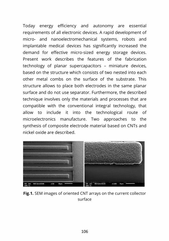
106
Today energy efficiency and autonomy are essential requirements of all electronic devices. A rapid development of micro- and nanoelectromechanical systems, robots and implantable medical devices has significantly increased the demand for effective micro-sized energy storage devices. Present work describes the features of the fabrication technology of planar supercapacitors – miniature devices, based on the structure which consists of two nested into each other metal combs on the surface of the substrate. This structure allows to place both electrodes in the same planar surface and do not use separator. Furthermore, the described technique involves only the materials and processes that are compatible with the conventional integral technology, that allow to include it into the technological route of microelectronics manufacture. Two approaches to the synthesis of composite electrode material based on CNTs and nickel oxide are described.
Fig.1. SEM images of oriented CNT arrays on the current collector surface

107
In the first case, oriented nanotube arrays were synthesized by PECVD on a pre-plating catalyst layer (Fig.1). After that, the nanotube surface functionalization was performed in argon-oxygen plasma, followed by thin nickel oxide layer deposition by SILAR. In the second case, carbon nanotubes were dispersed in alcohol solution and nickel oxide covering was produced by chemical precipitation; finally, composite material was selectively deposited to the current collectors by electrophoresis technique. The development of the second approach avoids the high-temperature processes of CNT arrays synthesis that is of particular importance when working with thermally sensitive components. On the other hand, the synthesis of oriented arrays on the current collectors’ surface allows to create more ordered structure, which has a positive influence on the power characteristics of the device.
PAMS-P4: Electrical and magnetic properties variations with high temperature treatment in Co-Ni mixed ferrite
Constantin Virlan1, Ovidiu-Florin Caltun2, Florin Tudorache3, Aurel Pui1
1Faculty of Chemistry, “Alexandru Ioan Cuza” University, Iasi, Romania 2Faculty of Physics, “Alexandru Ioan Cuza” University of Iasi, Romania 3Interdisciplinary Research Department – Field Science & RAMTECH, “Alexandru Ioan Cuza” University of Iasi, Romania
The aim of this study is to evaluate the structural and morphological changes that mixed ferrite undergo under high temperature treatment and to study the associated changes in their magnetic and electrical properties. Ferrites with the general formula Co1-xNixFe2O4, with x ranging between 0 and 1

108
where synthesized using the co-precipitation method in the presence of carboxymethylcellulose (CMC) as surfactant. The nanoparticles where initially calcined at 500 ºC, after which they were subjected to successive high temperature treatments at 700 ºC, 900 ºC and 1100 ºC [1] The nanoparticles were characterized using X-ray diffraction, transmission electron microscopy coupled with energy dispersive analysis and FT-IR spectroscopy. The magnetic properties were evaluated using a vibrating sample magnetometer, and the electrical properties were measured in terms of permittivity and conductivity in relation to applied electric field frequency and relative humidity (fig.1). Small variations in the magnetic properties and significant changes in the electrical properties were observed with increasing temperature for all samples. The variations can be assigned to changes in crystallite size, specific surface and porosity, characteristic for high temperature treatments [2].
[1] A. Pui, D. Gherca, N. Cornei, Mater. Res. Bull. 48 (2013) 1357–1362.
PAMS-P5: Upconversion luminescence in LaGaO3:Er:Yb synthesized by solid state reaction
Cristina Tihon, Serban Georgescu, Ana-Maria Voiculescu, Octavian Toma
Laboratory of solid-state quantum electronics, National Institute for Laser, Plasma and Radiation Physics, Magurele, Jud. Ilfov, 077125, Romania, Magurele, Romania
Lanthanum orthogallate LaGaO3 belongs to the wide group of the compounds of general ABO3 formula (A-rare earth ion, B - Al, Ga, Fe, Cr, V) and crystallise in a distorted perovskite

109
structure. LaGaO3 is an interesting host from the point of view of optical application [1]. This paper reports the synthesis and characterization of LaGaO3:Er3+:Yb3+. Lanthanum orthogallate LaGaO3 ceramic doped with Er3+ and Yb3+ was synthesized in our laboratory by solid state reaction, from stoichiometric quantities of high purity oxides (La2O3, Ga2O3, Er3O3, Yb2O3). The powders were mixed in agate mortar, pressed with a hydraulic press at 2MPa and then annealed in air at 1350 oC for 35 h. As a result of the thermal treatment, a solid, ceramic sample was obtained. The sample was cut, polished and washed in an ultrasonic bath to remove the abrasive particles. The sample was characterized by XRD and optical spectroscopy techniques (luminescence, diffuse reflectance and decay measurements).
[1]. Sokὁlska, Appl. Phys. B 71, 157-162 (2000).
PAMS-P6: Preparation and characterization of wavelength conversion thin filter by the spin coating method using fluorescence pigments for enhancing the efficiency of solar cells
Daisuke Watanabe, Shizutoshi Ando
Department of Electrical Engineering, Faculty of Engineering, Tokyo University of Science, 6-3-1 Niijuku, Katsushika, Japan
Solar cells have attracted attention as clean energy technologies using an inexhaustible solar energy. The solar cell module sold these days in the market has the energy conversion efficiencies of approximately from 14 to 18%. However, these energy conversion efficiencies were very low compared with that of nuclear power generation (33%) and

110
thermoelectric power generation (approximately 40%). One of an improvement of conversion efficiency, it is considered to improve various losses within a solar cell. The wavelength conversion filters are expected for increasing conversion efficiency of various solar cells. The method used fluorescent pigment. Formerly, in our group, we prepared the wavelength conversion filter on glass substrates by spin coating method using fluorescent dye with resin material (PMMA or FOSF). In this study, we tried to prepare the wavelength conversion filter by spin-coating method using fluorescent Pigments with ethylence-vinyl-acetate (EVA). In addition, we aimed to establish conditions for preparation. The mixed solution for wavelength conversion devices was prepared by mixing powder of fluorescent pigment (Lumogen F RED 305) and EVA, subsequently diluting by ethyl acetate, butyl acetate, 3-methoxybutanol and 3-methoxy-1-butanol. The glass substrates were spin-coated with the mixed solution at 3000 rpm for 10 sec to obtain precursor films with smooth surface. Finally, the heat-treated of the spin-coated films were carried out at 220℃ by IR lamp in order to obtain wavelength conversion devices.
PAMS-P7: Preparation and characterization of iron-oxide thin films by the coating thermal decomposition method
Mizuki Sunaga1, Felicia Iacomi2, Shizutoshi Ando1
1Department of Electrical Engineering, Faculty of Engineering, Tokyo University of Science, 6-3-1 Niijuku, Katsushika, Tokyo, Japan 2Faculty of Physics, “Alexandru Ioan Cuza” University of Iasi, 11 Carol I Blvd., Iasi, Romania
111
In nowadays, silicon (Si) based solar cells are occupied approximately 90% of the global market share of solar cells. However, the Si raw material has a serious problem that is the rise in prices and the supply shortage. Iron oxide (Fe2O3; hematite) is attracted much attention as a promising material for the light absorption layer of the next generation high conversion efficiency thin film solar cells, because it has a large absorption coefficient of the order of 105 cm-1, that is two orders of magnitude larger than that of crystal or amorphous silicon. This material is present inexhaustibly on the earth. In addition, harm to the human body is less, and is a material which is kind to the environment. In this work, Fe2O3 thin films were prepared by the Coating Thermal Decomposition method using an iron naphthenate as a raw material. The prepared Fe2O3 thin films were investigated the optimum manufacturing conditions by evaluating the surface state, luminous transmittance, and crystalline. Additionally, it tried to prepare titanium (Ti)-doped iron oxide (Fe2O3:Ti) films thin films in order to obtain n-type Fe2O3, and examined the effectiveness of Ti-doping. As the results, Fe2O3 thin film prepared on repetition of 5 times was shown the crystalline of α-Fe2O3 phase. The preparation by the pyrolysis process in the atmosphere of oxygen was useful for improvement in crystallinity of Fe2O3 and Fe2O3:Ti thin films.
PAMS-P8: The study of influence of the thermal annealing on the properties of PVDF coatings deposited by MAPLE
L.N. Dumitrescu1,2, I. Tirca1,2, V. Ion1, A. Moldovan1, V. Marascu1,3, V. Dinca1, M. Dinescu1

112
1Lasers, 1National Institute for Laser, Plasma and Radiation Physics, Magurele, Bucharest, Romania 2Physics, 2University of Craiova, Faculty of Sciences, Craiova, Romania 3Physics, 3University of Bucharest, Faculty of Physics, Magurele, Bucharest, Romania
Polyvinylidene fluoride (PVDF) is semi-crystalline fluoropolymer with (C2H2F2)n chemical formula. It possesses interesting characteristics like polymorhism and two important properties with distinct engineering advantages: firstly, the polymer's pyroelectricity, and secondly its piezoelectric properties [1], which are making it very attractive for a wide range of applications. In this work, we report preliminary results of influence of the thermal annealing of deposited polymer coatings on optical morphological and structural properties correlated with deposition parameters of PVDF thin films grown by matrix assisted by pulsed laser evaporation (MAPLE) at 266 wavelength. The thin films were deposited on various substrates as SiO2 Si, Pt/Si, for different investigations, using a frozen target with three concentrations (3%, 5%, 7%) of polymer in dimethyl sulfoxide (DMSO) matrix solvent. The resulted coatings were undergone to a series of thermal annealing and investigated in terms of morphology, optical, chemical structure and structural properties by atomic force microscopy ultraviolet–visible spectroscopy, spectroellipsometry, Fourier transform infrared spectroscopy and X ray diffraction. PVDF coatings with optical and structural characteristics resembling to the bulk material, in agreement with the literature [2] and suitable for different applications have been achieved.

113
[1]. H. Kawai, “The Piezoelectricity of poly(vinylidene fluoride),” Jpn. J. Appl. Phys., Vol. 8, pp. 975-976, 1969. [2]. Ajay Pal Indolia& M. S. Gaur, Optical properties of solution grown PVDF-ZnOnanocomposite thin films, J.of Poly.R
PAMS-P9: Characterization of the structural and optical properties of ZnO thin films doped with Ga and (Al+Ga)
Claudiu Lung1, Maria Toma1, Mariana Pop3, Daniel Marconi2, Aurel Pop1
1Solid State Physics, Babes-Bolyai University, Cluj-Napoca, Romania 2Department of Molecular and Biomolecular Physics, National Institute for Research and Development of Isotopic and Molecular Technologies, Cluj-Napoca, Romania 3Department of Material Science and Engineering, Faculty of Materials Engineering and Environment, Technical University, Cluj-Napoca, Romania
In this study we describe transparent conducting thin films of Ga-doped ZnO (GZO) and co-doped Al+Ga ZnO (GAZO), deposited by RF magnetron sputtering. This technique is often used to deposit thin films because of its efficiency, low cost and good reproducibility. The deposition was performed on glass substrates heated at a constant temperature of 150 oC, a magnetron power of 100 W and the deposition pressure was maintained at 2.1 × 10⁻² mbar. By modifying the distance between target-substrate for 4 cm, 6 cm and 8 cm and the type of dopant (Ga, Al+Ga), six samples were obtained. The influence of dopant upon crystallographic structure of the thin films was analyzed by X-ray diffraction. These results show that the obtained films were polycrystalline with a hexagonal wurtzite structure and preferentially oriented perpendicular to the substrate surface, in the (0 0 2) crystallographic direction.

114
Microstructural and chemical analysis (SEM, EDX) revealed that the type of doping and the distance between target and substrate modify the microstructure of thin films. Atomic force microscopy results show that the films have a uniform surface, with spherical grain structure. Optical transmission measurements showed an 85% transparency in the visible range, for the undoped ZnO films and the transparency of these films decreased when the dopant content was raised.
[1] Aslan Kh. Abduev, Akmed K. Akhmedov, Abil Sh. Asvarov, Solar Energy Materials & Solar Cells 91 (2007) 258–260). [2] Sidharam P. Pujari, Han Zuilhof, Applied Surface Science 287 (2013) 159– 164.
PAMS-P10: Characterisation and calibration of the optical thermometry properties of La2O2S:Eu phosphor material
Lucas Erasmus, Koos Terblans, Hendrik Swart
Physics, University of the Free State, Bloemfontein, South Africa
This study is focused on the measurement of the optical thermometry properties of Lanthanum Oxysulphide doped with Europium (La2O2S:Eu) phosphor material by utilising an in-house modified Photo-luminescence (PL) system. The optical thermometry properties of phosphor materials can be measured by several techniques, however the technique focused on in this presentation is the fluorescence intensity ratio technique where the fluorescence spectra of a phosphor material was obtained and the intensity ratio between two thermally coupled levels was monitored. This was done by studying the peak intensities of the different PL peaks due to

115
the different transitions from Eu3+ in La2O2S:Eu at temperatures ranging from 30 degrees Celsius to 200 degrees Celsius. It was clear that La2O2S:Eu can be used as a temperature sensor by using the calibration data. The viability of La2O2S:Eu as a stable and accurate temperature sensor was also evaluated by investigating it’s structural and chemical properties by utilising the X-ray Diffraction and X-Ray Photo-electron Spectroscopy techniques.
[1] Allison Remote thermometry with thermographic phosphors: instrumentation and applications. [2] Khalid Thermographic phosphors for high temperature measurements: principles, current state of the art and recent applications.
PAMS-P11: Picosecond and femtosecond laser ablation plasma plumes investigated by time-resolved optical and electrical methods
Stefan-Andrei Irimiciuc1,2, Silviu Gurlui2, Petru Nica3, Maricel Agop3,2, Cristian Focsa1
1Physique des Lasers, Atomes et Molécules, Université Lille 1, Lille, France 2Faculty of Physics, "Alexandru Ioan Cuza" University of Iasi, Iasi, Romania 3Departament of Physics, "Gh. Asachi" Technical University of Iasi, Iasi, Romania
Transient plasmas generated by picosecond and femtosecond laser ablation on several metals (Mn, Ni, Cu, Ti, Ni and Al) were investigated through optical and electrical methods. The aim of these experiments was to perform time-resolved investigations on laser-produced plasmas and understand the effect of the target physical properties on the dynamics of the plasma
116
plumes. The experiments were performed in similar conditions regarding the background pressure (p = 10-5 Torr) and probe-target axial distances (1mm - 30 mm). The time-resolved -optical investigations were focused on recording snapshots of the laser-produced plasmas at different time delays in respect to the ablation laser pulse, in order to investigate the structure of the plasma plumes in their global dynamics. By applying different biases on the probe and collecting the corresponding current one can reconstruct the I-V characteristics at different time delays. From this we were able to determine the temporal evolution of various plasma parameters which present different behaviors for the plasmas produced in picosecond and femtosecond regimes. The ionic current temporal traces are discussed in terms of a shifted Maxwell-Boltzmann distribution function, offering the possibility to determine other parameters such as the ion temperature and the drift velocity. The target physical properties (electrical and thermal conductivities) were proven to have a significant influence on the plume dynamics like expansion velocity, electron temperature or plasma potential.
PAMS-P12: Characterization of graphene-PDMS nanocomposite films
Ioana-Luciana Punga1, George-George Rusu1, Gabriela Borcia1, Mirela Suchea1, Adrian Bele2, Daniel Timpu2, Maria Cazacu2, Felicia Iacomi1
1Faculty of Physics, “Alexandru Ioan Cuza” University of Iasi, Romania 2Macromolecular Chemistry, Institute of Macromolecular Chemistry “Petru Poni”, Iasi, Romania

117
Composite- and nanocomposite-materials have been manufactured using a variety of and reinforcements, conducting to a remarkably wide range of properties. Among these, polymer nanocomposites have great potential, being thought of as the materials of the 21st century. As filler, graphene offers many functions due to the excellent electrical conductivity and superb mechanical properties, which arise from its particular two-dimensional crystallographic nature. These properties along with the large specific area and the ability to modify the behavior of the underlying graphene by the use of polymer composites, have integrated this material in polymer nanocomposites for energy storage systems, biological or physical sensors, and biomedical applications. Nonetheless, a convenient combination of graphene and polymer depends heavily on the dispersion of the two components within the composite structure. In general, the aim in formulating a polymer nanocomposite is to achieve a uniform particle size distribution and minimal agglomeration of the nano-reinforcement. Taking this into account, a study on graphene-based polymer nanocomposites, which can be produced in bulk quantities by chemical methods, was carried out. Nanocomposite films with different graphene content were obtained using polydimethylsiloxane (PDMS) as polymeric matrix. The optical, morphological and structural properties were studied using XPS, XRD, SEM, Raman spectroscopy and light transmission measurement. Also, the relationship of these properties with the graphene�polymer interactions and the graphene dispersion in the polymer matrix was analyzed.

118
PAMS-P13: Synthesis of soft magnetic electrically isolated materials
Elena Chitanu, Mirela Maria Codescu, Delia Patroi, Eugen Manta, Wilhelm Kappel, Jana Pintea
Advanced Materials, R&D National Institute for Electrical Engineering, ICPE-CA, Bucharest, Romania
The concept of more electrical aircraft architecture requires new magnetic materials, with improved magnetic and electrical properties. The paper investigates the soft magnetic materials based on FeCo/Al2O3 core-shell nanoparticles, synthesized by sol-gel technique. These nanomaterials combine the high saturation magnetisation of FeCo compound with the increased resistivity of Al2O3 and allow the decreasing of magnetic losses for the bulk sized components, compared with the currently available Fe-Si alloys, used as metallic punched sheets for the building of the magnetic cores in electrical machines. The main physical characteristics of the Fe-Co/Al2O3 prepared nanomaterials are: saturation magnetisation in the range of 100 -165 emu/g, coercivity around 14.35 kA/m and resistivity in the range of 5,50 - 17,50 Ω•m.
PAMS-P14: Magnetic properties and magnetocaloric effect on Ce1-xYxFe2
Gabriela Souca, Roxana Dudric, Sever Mican, Romulus Tetean
Condensed Matter Physics and Advanced Technologies, Babes-Bolyai University, Faculty of Physics, Cluj-Napoca, Romania
Structural, magnetic properties and magnetocaloric effect of Ce1-xYxFe2 compounds have been investigated. The powder X-

119
ray diffraction measurements show that all samples are single phase and crystallize in a cubic Laves type structure with the space group Fd3m. The lattice parameter was found to increase slowly with the yttrium content. The magnetic measurements were performed in magnetic fields up to 12 T in the temperature range 4.2-300 K. The temperature dependence of the magnetization in zero field cooling (ZFC) and field cooling (FC) modes were recorded under a magnetic field of 0.05 T. The compounds are ferromagnetically ordered. The Curie temperatures of the alloys are increasing with Y content. Values of Tc= 247 K for x=0.1 and Tc=277 K for x=0.15 were determined. At 4.5 K the saturation magnetisation was found to be 2.69 µB/f.u. for x=0.1 sample and 2.68 µB/f.u. for x=0.15 sample. Considering that the iron magnetic moment is not affected by alloying having the value of 1.46 µB/at [1], the Ce magnetic moment was determined. Values 0.25 µB/at for x=0.1 and 0.28 µB/at for x=0.15 were obtained. The maximum values of the magnetic entropy change, 2.55 J/KgK for x=0.1 and 2.15 J/KgK for x=0.15, are located at temperatures near the magnetic transition ones and decrease with Y content. The magnetic cooling efficiency was evaluated by calculating the relative cooling power (RCP) based on the magnetic entropy change. The significant RCP values obtained, 135.15 J/kg for x=0.1 and 144.05 J/kg for x=0.15, and the absence of magnetic hysteresis suggest the possibility to use these materials for magnetic refrigeration devices in the room temperature range.
[1] A.P. Murani, Physica B 345 (2004) 89–92.

120
PAMS-P15: Characterization of Ni1-xZnxFe2O4 thin films deposited by spin coating
Mihaela Irimia, Mihaela Toma, Marius Dobromir, Valentin Nica, Ovidiu Chiscan, Felicia Iacomi
Faculty of Physics, "Alexandru Ioan Cuza" University of Iasi, Romania
Zinc doped Nickel ferrite (Ni1-xZnxFe2O4 with x = 0.0, 0.4, 0.6, 1.0)) nanostructured thin films with a thickness of 200 nm have been prepared by spin coating method using precursor solution containing metal acetates and an organic complexant (N-N-dimethylformamide). As a substrate we used microscope glass slides and alumina. The effect of the Zn content on structural, morphological, optical, magnetic and electrical properties of the films was investigated. XRD patterns showed that Ni1-xZnxFe2O4 thin films were polycrystalline exhibiting a single phase spinel structure. The lattice parameter decreases with increase of Zn content resulting in a decrease of lattice strain. The VSM measurements performed at room temperature show that Ni1-xZnxFe2O4 thin films exhibit a ferromagnetic behaviour. A dependence of the Ms, Mr and Hc values on Zn content was observed and can be attributed to the way in which Fe2+, Ni2+ (ferromagnetic ions) and Zn2+ (non-magnetic transition metal ion) are distributed in tetrahedral and octahedral sites. The transmission and reflection spectra, in the spectral range 300 – 1200 nm, have been investigated. All the studied thin films present a high transmittance, over 80%, and are poorly reflective. The absorption spectra of the films showed that these compounds are direct band gap material and the values of optical band gap increases with the increase
121
of Zn content. This behaviour could be explained on the basis of decrease in lattice parameter due to increase in Zn concentration. The electrical conductivity of Ni1-xZnxFe2O4 thin films has been investigated as a function of temperature, using two probe method. Using the temperature dependence of electrical conductivity data, the mechanism of electrical conduction was discussed. We also observed that the values of electrical conductivity are depending on Zn concentration Ni – Zn ferrite films deposited by spin coating method might have a high potential for application as transparent magnetic semiconductors.
PAMS-P16: Evolution of materials for clothing
Zoreslava Zakhozhai
Institute for Modern Technologies, Kyiv National University of Technologies and Design, Kyiv, Ukraine
The world's dynamic evolution of textile fibers and fabrics has been considered. An ancient man taught primitive way of processing skins of animals due to the need of clothing. Wool, cotton, linen were the first natural materials for clothes. China was mastered the secret production of natural silk (protein fibers) on BC. Since the late nineteenth century a wide intervention of chemistry and physics in a structure of macromolecules take place. In particular, the technological processes were developed for synthetic fibers based on natural polymers (viscose, acetate, etc). In the mid-twentieth century the technological processes were developed for synthesis of fiber-monomers, polymers, melts of synthetic polymers (nylon,
122
polyester, polyamide, polyacrylonitrile fibers). The current state of chemical fibers production began from the end of twentieth century. The IV generation of so-called "fibers for future" innovative materials were created, such as nanofibers, "intelligent textiles". Properties of the modern "intelligent textiles" responded to changes in the parameters of the internal and external environment [1]. Nowadays, metamaterials make the real revolution in evolution of properties [2]. The main feature of these materials is negative refractive index (Fig. 1), which takes place at simultaneous negative dielectric and magnetic permeabilities. Creation and using the metamaterials has very broad application prospects.
[1]. George G. Bogdanov, Zoreslava V. Zakhozhai. Evolution of Materials for Clothing. Kyiv, KNUTD, 2009 - 280 pages. [2]. http://en.academic.ru/dic.nsf/enwiki/11597380.
PAMS-P17: Synthesis, structural, electronic, and magnetic properties of α"-Fe16-xMxN2 (M=Fe, Ti, Zr) (M=Fe, Ti, Zr)
Roxana Alina One, Viorel Pop, Sever Mican, Diana Benea
Faculty of Physics, Babeş-Bolyai University, Cluj-Napoca, Romania
The recent rare-earth crisis led to an opening of various research directions for developing novel rare-earth free magnetic materials and environmentally friendly synthesis methods. We focused our attention on Fe-N based materials, specifically the α”-Fe16N2 phase. In this work we investigate the effect of doping and synthesis method on the structural, electronic and magnetic properties of α”-(Fe1-xMx)16N2 (M=Fe, Ti, Zr). Two synthesis routes are proposed: mechanical milling and
123
a route based on the sol-gel method. These two methods are applicable in industry and are based on cheap, available precursors and ammonia (NH3). Mechanical milling was used to prepare both pure and doped α"-Fe6-xMxN2 (M=Ti, Zr; x=0 and 0.05), while the sol-gel method was used to prepare only undoped α”-Fe16N2. Powders of Fe, Fe0.95Ti0.05 and Fe0.95Zr0.05 were obtained by milling stoichiometric powder mixtures in a high-energy planetary mill under Ar atmosphere. A xerogel was prepared via the sol-gel method using FeCl3, sucrose and pectin as precursors. The Fe2O3 powder was obtained after annealing the xerogel at 450 ºC for 12 h in air. The obtained powders were annealed under a mixed Ar/H flow at 400 ºC for 12 h, followed by annealing in anhydrous ammonia (NH3) flow at lower temperatures around 150 ºC for 24 h. X-ray diffraction results showed that the annealed powders were comprised of an α”- type majority phase, along with small amounts of unreacted iron and other nitrides. A higher α” phase concentration was obtained for the sample prepared through the sol-gel method, possibly due to the smaller particle size of the annealed powder. Electronic structure calculations have shown that the substitution of Fe with Ti or Zr increases the stability of the α”-Fe16N2-type phase over 200 ºC. An average Fe magnetic moment between 2.3 and 2.6 μB/atom was obtained, in good agreement with the experimental results. The effects of preparation route and dopant type on the structural, electronic and magnetic properties of α”-type phase are discussed.

124
PAMS-P18: Spin susceptibility of disordered gapped graphene systems
I. Grosu, T.L. Biter
Physics, "Babeș-Bolyai" University, Cluj-Napoca, Romania
We calculate the spin susceptibility for the case of gapped graphene systems in the presence of disorder. The average single-particle density of states in gapped graphene with disorder was calculated using the Born and the T-matrix approximations. The temperature dependence of the static spin susceptibility was analysed and the influence of the chemical potential and disorder is also discussed.
PAMS-P19: Transport through a quantum dot with electron-phonon interaction
Levente Máthé, Ioan Grosu
Physics of Condensed Matter, Babeș-Bolyai University, Cluj-Napoca, Romania
We theoretically study, in different particular cases, the electrical transport properties of a single level quantum dot connected to two normal conducting leads, which is coupled to the lattice vibrations, thus their electrons can interact with these phonon modes. We determine the current through the quantum dot in three different situations: time-dependent, time-independent and time-averaged. In all situations we consider three cases: when there is no electron-phonon interaction, or the dot electrons interact with optical phonons or with acoustic phonons. Each situation is performed for zero and non-zero temperatures, while at finite temperatures we

125
take into account the temperature dependence of the chemical potential. We treat the electron-phonon interaction by the canonical transformation method and neglect the effect of electron-phonon interaction on the tunneling of electrons from the metallic contacts to the dot. So we separate the electron-phonon interaction term in the Hamiltonian into two parts which do not interact directly. We present our results for different values of the relevant parameters except for the total time-dependent case. In the time-independent non-interacting case the current has a Lorentzian shape, while when the dot electrons interact with the longitudinal optical phonons in the spectrum appears a subpeak. The position of subpeak depends on the phonon frequency. In the case of electro-acoustic phonon interaction, the spectrum is continuous. In the time-averaged case the interpretation of the phonon spectrum is more difficult due to the external modulation effects. There appear many parasite peaks. Thus the transport properties of dot strongly depend on the time-dependent bias.
[1] Levente Máthé, Transport through a quantum dot with electron-phonon interaction, Master Thesis, „Babeș-Bolyai” University Cluj-Napoca, Faculty of Physics, 2016. Scientific supervisor: Prof. dr. Ioan Grosu
PAMS-P20: Study on some iron oxide nanoparticles and their cytotoxicity
Gabriela Vochita1, Cosmin Mihai1,2, Emil Puscasu3, Liviu Sacarescu4, Daniela Gherghel1, Dorina Creanga3
1Institute of Biological Research, Iasi, Romania

126
2Interdisciplinary Research Department – Field: Science, “Alexandru Ioan Cuza” University of Iasi, Romania 3Physics Department, “Alexandru Ioan Cuza” University of Iasi, Romania 4Laboratory of Inorganic Polymers, “Petru Poni” Institute of Macromolecular Chemistry, Iasi, Romania
Iron oxide nanoparticles (IONP) were yielded by chemical route and stabilized with oleate in aqueous suspension. Their microstructural and magnetic properties were investigated by Transmission Electron Microscopy (TEM), Small Angle X-ray Scattering (SAXS), X-Ray diffractometry (XRD) and Vibrating Sample Magnetometry (VSM). Cytotoxicity was tested on murine cell line by flow cytometry and gel electrophoresis; oxidative stress induced by IONP in animal cells was investigated by the assay of some antioxidant enzymes.
Fig.1. TEM image of IONPs
TEM data evidenced quasi-spherical particles up no larger than 45 nm (Fig. 1). SAXS investigation results were modeled with NanoFit software based on non-linear least-squares data analysis confirming microscopy observations. Spinel structure was revealed by XRD while superparamagnetic features were

127
emphasized by VSM recording. Flow cytometry analysis showed induced apoptosis and gel electrophoresis showed DNA fragmentation. Catalase (CAT) and glutation peroxidase (GPx) activities increasing have suggested the generation of reactive oxygen species, which enhanced to the increase of the IONP suspension concentration (Fig. 2).
Fig.2. The antioxidant enzymes activities as response of living
cells to IONPs supply
The graph in Fig. 2 suggested the catalytic action of iron ions released following endocytosis of IONPs supplied to murine cells. The results are of interest from the view point of side effects of magnetic nanoparticles utilized in biomedical applications such as magnetically assisted drug delivery, magnetic resonance imaging with magnetic nanoparticles as contrast agents or in hyperthermia treatment of tumor cells.
PAMS-P21: Ellipsometric investigation of Ca doped ZnO thin films deposited by sol-gel on oxidized Si substrates: multilayer modeling
Constantin Florin Comanescu, Munizer Purica
Micro-Nano photonics Laboratory, IMT Bucharest, Bucharest, Romania
128
Transparent conductive oxides (TCO) are still widely investigated by taking into account the preparation method, the doping element and level of concentration, the annealing temperature and deposition substrates. In this paper we present the results of spectroscopic ellipsometry investigation of ZnO and Ca doped ZnO layers synthesized by sol gel method in order to refine the optical model and corresponding dispersion theories to determine accurately the optical constants – refractive index (n) and extinction coefficient (k). The ZnO:Ca layers were prepared by means of sol-gel method in 5 steps, each step consisting in spinning followed by thermal annealing at 500 °C for 5 minutes. The target substrate is oxidized silicon, the oxide thickness being 305 nm and the Ca doping percents are 0%, 1% and 5%. The ZnO:Ca samples have been modeled by using a multilayered structure consisting in 4 layers: ultra-thin layer corresponding to surface roughness, a layer of Ca doped ZnO, silicon oxide (305 nm) and silicon substrate. The surface roughness and Ca doped ZnO were modeled by means of effective medium approximation (EMA) and a Cauchy layer in the spectral range 300-850 nm. The thickness corresponding to undoped ZnO layer is ~107 nm having a refractive index of 1.955 at 632 nm and a roughness of ~20nm. The thickness corresponding to ZnO:Ca 1% layer obtained by sol-gel is ~200 nm having a refractive index of 1.7 at 632 nm and a roughness of ~30nm. The thickness corresponding to ZnO:Ca 5% layer obtained by sol-gel is ~290 nm having a refractive index of 1.9 at 632 nm and a roughness of ~3nm. The smallest roughness and the layer with highest

129
thickness is corresponding to the samples with 5% Ca doped ZnO.
Acknowledgement This research was supported by PNII-PT-PCCA-2013-4-2104-D1-NANOZON (Contract no. 27/2014) and by IMT CORE program TEHNOSPEC.
PAMS-P22: Hybrid halide perovskite based solar cells
D. Dogaru1,2, C. Besleaga, V. Stancu, A. G. Tomulescu, M. Sima, L. Pintilie, I. Pintilie 1Laboratory of Multifunctional Materials and Structures, National Institute of Materials Physics, Măgurele, Romania 2Faculty of Physics, University of Bucharest, Romania
The vast potential of hybrid organic-inorganic perovskite materials gives rise to great opportunities for photovoltaic applications. However, there are lots of puzzles to unravel in order to better understand the working principles which govern devices operation. Regarding the basic fundamentals of perovskite materials, results on the structural, optical and electrical characterization of hybrid perovskite thin films, in particular the methyl-ammonium lead halides are presented.
PAMS-P23: A model for the current-voltage characteristics of a thin film metal-ferroelectric-metal structure
Dorin Rusu, Lucian Pintilie
Laboratory of Multifunctional Materials and Structures, National Institute of Materials Physics, Magurele, Romania To aid our understanding of current voltage characteristic of a thin film metal-ferroelectric-metal a model was constructed.
130
Polarization is considered as 2 charged sheets of opposite sign situated near the electrode interface at a distance that defines a layer absent of switchable polarization. Leakage current is obtained by considering the charge flow through its interfaces. To this end Poisson equation was used in order to find the potential energy profile throughout the structure, polarization playing a key role in controlling its form. The resulting characteristic is in good agreement with the experimental data obtained at different temperatures. Both thermionic and tunneling current components are considered, suggesting the interface nature of the leakage current, and the idea of existence of an interfacial layer characterized by a low dielectric permittivity is supported by some fit parameters values.
[1]. Lucian Dragos Filip, Lucian Pintilie, Eur. Phys. J. B (2016) 89: 44; [2]. S.M Sze, Physics of Semiconductor Devices (Wiley, New York, 1981). [3]. E.L. Murphy, R.H. Good, Phys. Rev. 102, 1464 (1956).
PAMS-P24: Study of physical properties of rf-sputtered ZnSe thin films
Ana-Maria Raduta
Faculty of Physics, University of Bucharest, Bucharest, Romania
ZnSe thin films were deposited by rf-magnetron sputtering technique onto optical glass substrates. The induced effects of deposition time were determined, taking into account a 10 – 4 minutes range, while working power, pressure and substrate temperature were maintained constant. With good mechanical and chemical properties these kinds of layers can be

131
successfully used in the architecture of various electronic and optoelectronic devices, like photovoltaic cells. A slightly decrease of optical bandgap with the decrease of deposition time was noticed in the 300 – 900 nm range. The X-ray diffraction investigations proved that our fabricated ZnSe thin films have a well-defined crystalline structure, with a preferential growth direction – (111). The roughness average and root-mean-square values were determined by atomic force microscopy (AFM), in non-contact mode, and their small values proved that rf-magnetron sputtering is a suitable method in order to obtain smooth and uniform thin films. To fully understand the induced effects of deposition time on the physical properties of rf-sputtered ZnSe thin films, for-points electrical measurements were performed in the 300K – 30K temperature range and electrical parameters like charge carriers’ mobility were calculated and discussed.
PAMS-P25: Vibrational characterization of capecitabine and its active moiety 5-fluorouracil by SERS and DFT
Mihaela Chiş1, Alois Bonifacio2, Valter Sergo2, Călin Căinap3, Vasile Chiş1, Monica Baia1
1Faculty of Physics, Babeş-Bolyai University, Cluj-Napoca, Romania 2Department of Engineering and Architecture, University of Trieste, Trieste, Italy 3Medical Oncology, The Oncology Institute "Prof. Dr. Ion Chiricuţă", Cluj-Napoca, Romania
Capecitabine (CAP) is a prodrug of the anti-metabolites group, used in treating breast, gastrointestinal and genitourinary tracts cancers. [1] CAP is selectively tumor-activated, being dependent on enzymes which have generally higher

132
concentrations in tumor tissue than in healthy tissue. Its anti-metabolic activity starts as a result of it being converted to 5-fluorouracil (5-FU) which interferes with the production of new DNA. [2] The cytotoxicity of this type of drugs, the different patients’ metabolism and other circumstantial factors for each treatment underline the importance of Therapeutic Drug Monitoring in chemotherapeutic treatments. [3] The vibrational characterization of drugs and their metabolites is a useful approach that facilitates their detection in multi-component systems like body fluids. Surface Enhanced Raman Spectroscopy, SERS, provides rich vibrational information making this technique highly useful in identifying and quantifying drugs and their metabolites in body fluids. In this study, Raman and SERS techniques coupled with density functional theory (DFT) calculations were employed in order to obtain the vibrational characterization of the two molecules (Fig.1). Firstly, we performed Raman measurements on the powder form of CAP, then SERS measurements on aqueous solutions of the compound and the lowest detectable concentration was found to be 0.5�10-9M. The same measurements were employed on 5-FU in order to obtain a reliable comparison between the two compounds. This comparison could eventually enable the distinction between the drug and its metabolite in future analysis of more complex samples from clinical environment.

133
DFT calculations were employed in order to achieve a precise vibrational assignment of the experimentally observed Raman bands of the investigated compounds.
Fig.1. SERS spectrum of 10-1 M CAP-water solution (a), Raman
spectrum of CAP powder (b) and calculated Raman spectrum of the CAP molecule in gas-phase (c)
[1] C.M. Walko, C. Lindley, Clin. Ther. 7, 2005, 23. [2] M. Breda, S. Barattè, Anal. Bioanal. Chem. ,397, 2010, 1191 [3] L. Lennard, Br. J. Clin. Pharmacol. 52, 2001, 75S.
PAMS-P26: Conduction in ferroelectric state of TGS crystal
Marinel Dan1, Horia Alexandru1, Paul Ganea2
1Faculty of Physics, University of Bucharest, Bucharest, Romania 2National Institute of Materials Physics, Magurele, Bucharest, Romania
134
Triglycine sulphate crystal (TGS) is a ferroelectric having a Curie point at 49.2°C. In the pure state, crossing down the transition point, TGS crystal has a metastable state. Single crystal TGS was grown at 52°C, in the paraelectric phase, where no mechanical tensions due to ferroelectric domains were present. Dielectric properties of a pure TGS sample were measured on the frequency 1 Hz-10 MHz range, during the temperature decrease from 65°C towards the room temperature, at a constant rate of 0.6°C/min. The real and imaginary component of permittivity were measured and the conduction component of ε” was estimated. The Influence of conduction on the dielectric parameters, like the relaxation times and the Cole-Cole constants of the two main component of permittivity were evaluated. Strikingly, the parameters have particular dependences on several ranges of temperature. Here, we present the influence of conduction on the assembly of experimental data on a large frequency range (1-10 7 Hz), down the Curie point till the room temperature. The main temperature range, where the dielectric parameters changes are around 35-37, 40-41 and 45-46 °C and seem to be related with the lattice dynamic.
PAMS-P27: Study of physical properties of P3OT:F-SWCNTs based photovoltaic cells
L. Dan1, J. Al-Zanganawee2, S. Iftimie1, A. Radu1, S. Antohe1,3, M. Enachescu2,3
1Faculty of Physics, University of Bucharest, Bucharest, Romania 2Center for Surface Science and Nanotechnology (CSSNT), University Politehnica of Bucharest, Bucharest, Romania 3Physics Department, Academy of Romanian Scientists, Bucharest, Romania

135
We report the fabrication and study of performances of P3OT:F-SWCNTs based photovoltaic cells, obtained by spin-coating. The single wall carbon nanotubes functionalization (F-SWCNTs) was done using nitric acid and was confirmed by thermogravimetric measurements (TGA) and scanning electron microscopy investigations (SEM). The active layer of our fabricated cells was tuned by varying the added F-SWCNTs percentage: 1%, 2% and 4%, and their photovoltaic performances were compared with those obtained for P3OT individual layer based PV cells. Specific parameters like short-circuit current density, open circuit voltage and fill factor were calculated and discussed. An optimal percentage of 2% was determined in the case of our prepared structures. The open circuit voltage values were higher for all P3OT:F-SWCNTs samples compared with P3OT ones, proving that the addition of functionalized single wall carbon nanotubes increases the overall electrical conductivity of fabricated photovoltaic cell by creating supplementary charge carriers’ transportation ways. Moreover, the external quantum efficiency values were bigger for all samples having F-SWCNTs:P3OT active layer proving these blends with high homogeneity could be successfully used to the preparation of bulk-heterojunction photovoltaic cells with improved efficiency and stability. Keywords: P3OT, F-SWCNTs, PV cells.
PAMS-P28: Structural and optical properties of Ni, Co doped ZnO thin films
Mihaela Toma1, Mihaela Irimia1, Daniel Timpu1, Lucian Mihai Cosovanu1, Ovidiu Vasilovici1, Florin Enescu1, Vasile Tiron1, G.G. Rusu1, Marius Dobromir1, Felicia Iacomi1
136
1Faculty of Physics, Al. I.Cuza" University of Iasi, Romania 2Petru Poni Institute of Macromolecular Chemistry, Petru Poni Institute of Macromolecular Chemistry, Iasi, Romania
Nanocrystalline thin films of low Ni, Co doped ZnO were deposited onto glass and quartz substrates by using a spin coating method. Post-annealings were performed at 450qC for thin films deposited on glass substrate and 650 qC for those deposited on quartz substrate. Structural and optical properties were investigated by using, X-ray diffraction, X-ray photoelectron spectroscopy and UV-VIS. The surface morphology, roughness and piezoelectric properties were investigated by atomic force microscopy and showed the influence of dopant nature and annealing temperature. At low doping level, local structure remains identical to ZnO with subtle increase in the bond length. XPS investigation indicates valence +2 both for Ni and Co. The optical properties were investigated in detail. Our results revealed an influence of the Co and Ni doping level on the optical parameters of the ZnO thin film.
PAMS-P29: Accurate Raman Spectra for aniline derivatives by anharmonic computations
Ana-Maria-Raluca Gherman1, Loredana F. Leopold2, Vasile Chiş1
1Faculty of Physics, Babeş-Bolyai University, M. Kogălniceanu 1, RO-400084, Cluj-Napoca, Romania 2Faculty of Food Science and Technology, University of Agricultural Sciences and Veterinary Medicine, Mănăștur 3-5, 400372, Cluj-Napoca, Romania
Anilines are organic materials which play an important role in the industrial chemicals, especially dyes. Characterizing

137
geometrical and electronic structure of such molecules brings valuable information for further investigations in different chemical reactions (Fig.1). Aniline, p-cyanoaniline, p-nitroaniline, and p-methylaniline are subjects of the study of their Raman spectra. Similar features are present in all four experimental spectra due to the much alike molecular structures, but subtle features, characteristic for each molecule, are to be explained also in great detail by quantum chemical calculations. Quantum chemical calculations were performed with Density Functional Theory (DFT) approach, using B3LYP functional. Frequency calculations were performed at both harmonic and anharmonic approximations on monomers. PCM solvation model was used with water as solvent. Anharmonic calculations employing second-order vibrational theory are good compromise between high accuracy and computational costs when performed together with B3LYP hybrid exchange-correlation functional, without the need of using empirical scaling factors. Subtle experimental vibrational features of all four molecules have been very well explained based on quantum chemical calculations performed on adequate models, using the Gaussian program package [1].
Fig.1. Aniline derivatives

138
[1] Gaussian 09, Revision E.01, M. J. FRISCH et al., Gaussian, Inc., Wallingford CT, 2009.
PAMS-P30: The degradation effect of a plasma micro-jet discharge at the interaction with organic dyes E. Muntean, I.E. Vlad, S.D. Anghel
Faculty of Physics, Babeș-Bolyai University, M. Kogălniceanu 1, 400084 Cluj-Napoca, Romania
Plasma plays an important role in many industrial, medical and technological applications. The purpose of this work was to study the degradation effect of the plasma jet discharge at the interaction with various dyes. Moreover, the evolution of the pH and the electrical conductivity of the solutions were also monitored. The plasma jet was diagnosed by identifying the atomic and molecular species found in the discharge and by measuring its characteristic temperatures. The discharge used in this study is a µ-jet plasma discharge generated using a 10.2 MHz excitation frequency at 2 kV voltage, using Helium as the plasma gas. The discharge takes place at the surface of the liquid and according to UV-Vis emission spectra it contains He, N2, H, O and OH radicals. The oxidative species (OH, O, HO2 or H2O2) and the UV radiation generated at the interaction between the µ-jet and the liquid lead to the degradation of all the studied dyes. The main process responsible for the discoloration is the breaking of the chromophore groups found in their molecular structure. The degradation process of the dyes continues even after the plasma treatment stops and the presence of the dye doesn’t influence in any way the changes in pH and electrical conductivity that occur in the treated liquid.

139
PAMS-P31: Magnetic hyperthermia characterization of magnetite, maghemite and hematite magnetic nanoparticles
Alin Iulian Moldovan1, Cristian Iacovita2, Rares Stiufiuc1, 2, Romulus Tetean3, Constantin Mihai Lucaciu1
1 Department of Bionanoscopy, MedFuture Research Center for Advance Medicine, “Iuliu Hatieganu” University of Medicine and Pharmacy, Pasteur 4-6, 400337 Cluj-Napoca, Romania. 2Department of Pharmaceutical Physics-Biophysics, Faculty of Pharmacy, ‘‘Iuliu Hatieganu’’ University of Medicine and Pharmacy, Pasteur 6, 400349 Cluj-Napoca, Romania 3Department of Solid State Physics and Advanced Technologies, Faculty of Physics, ‘‘Babes Bolyai’’ University, Kogalniceanu 1, 400084 Cluj-Napoca, Romania
Magnetic nanoparticles (MNPs) represent one of the main classes of nanoparticles (NPs) which are currently in the research spotlight, with many potential applications in the field of life sciences: magnetic resonance imaging contrast enhancement, tissue repair, immunoassay, detoxification of biological fluids, drug delivery, hyperthermia, and cell separation. The most widely investigated MNPs are mainly iron oxides: magnetite (Fe3O4) and maghemite (γ-Fe2O3). However, in nature, the most frequent iron oxide polymorph is hematite (α-Fe2O3), which has strong thermodynamic stability. We have successfully synthesized Fe3O4 MNPs by means of the solvothermal reduction method employing biocompatible polyethylene glycol (PEG200) as a solvent. MNPs exhibit a polyhedral shape (cubic, octahedral) with a mean size of 50 nm as revealed by TEM analysis. Maghemite NPs have been obtain by annealing the magnetite MNPs at 250°C for 4h. Upon

140
annealing the morphology and size of MNPs was not affected. The further annealing of the magnetite NPs at 550 °C for 6 h induces the formation of hematite NPs in large aggregates. For comparison, we have also synthesized superparamagnetic Fe3O4 MNPs, by means of thermal decomposition of iron acethylacetonate in oleylamine and oleic acid. These MNPs display predominantly a spherical shape with a diameter around 10 nm. The oxidation degree of each type of MNPs we have been verified by employing Raman spectroscopy. The heating efficiency of the MNPs, quantified by the specific absorption rate (SAR), has been evaluated in the presence of an alternating magnetig field of 355 kHz and amplitudes (H) between 5 kA/m to 65 kA/m, in an envirenment held at 37°C. The SAR values of the superparamagentic Fe3O4 MNPs increase from 4 W/gFe to 320 W/gFe as the H increaseas, following almost a linear dependency with H2. Since the polyhedral Fe3O4 MNPs are ferromagnetic at room temperature and above, their SAR values display a sigmoidal shape reaching saturation of ~1900 W/gFe at about twice the coercive field. A similar behaviour is recorded for maghemite MNPs, but the saturation value of SAR drops to ~1400 W/gFe. Hematite NPs, as they are antiferromagentic, do not deliver heat upon exposure to an AC magnetic field.
Acknowledgements: This research was supported by the Romanian National Authority for Scientific Research, CNCSIS-UEFISCDI, project nos. PN-II-ID-PCE-2012-4-0531, PN-II-ID-PCE-2011-3-0954 and PN-II-RU-TE-2014-4-1770.

141
Plenary Session (PL)
Hall 1: George Calugareanu Amphitheater
PL21: Photovoltaic cells based on organic and hybrid biologic/polymeric thin films
Stefan Antohe1,2
1Faculty of Physics, University of Bucharest, Magurele, Romania 2Physics, Academy of Romanian Scientists, Bucharest, Romania
In the last decades the photovoltaic cells based on organic and biologic thin films have attracted a great deal of interest to produce efficient and low-cost solar cells. Among the organic semiconductors envisaged to be used in such structures, small molecules like metal-doped phthalocyanines (MePc, with Me=Cu, Mg, Zn, etc.) and polymers are the most studied. As biologic semiconductor, the Chlorophyll-a is a potential candidate for photovoltaic structures. The optical absorption of these materials in the visible range of the solar spectrum is strong, but based on an excitonic mechanism. Due to the small diffusion length of the exciton in organic semiconductors (30-80 nm), to achieve a good efficiency in light absorption, the absorber layer has to be at least 100 nm thick. This inconvenient could be avoid, by the preparation of the multilayered structures containing different organic and biologic absorbers, or creating a large number of Donor/Acceptor Interfaces, spread in the whole volume of the composite absorber, leading to so called “Bulk heterojunction” cells. In this work are summarized the electrical and photoelectrical properties of the photovoltaic cells based on

142
the organic (small molecules and polymers) and biologic thin films. First the single-layer structures (ITO/CuPc/Al and ITO/TPyP/Al) have been prepared and characterized. The double-layer structures like, ITO/CuPc/TPyP/Al and ITO/Chl a/TPyP/Al, exhibits stronger spectral sensitivity having a power conversion efficiency with about two orders of magnitude, higher than previous one. Three-layered organic solar cells with an interlayer of co-deposited dyes of p-type CuPc and n-type TPyP, between the respective dye layers, showed increased power conversion efficiency. The structures based on the P3HT: PCBM (1:1) blend and the hybrid structures of Chl/:P3HT:PCBM(1:1) shows a promising photovoltaic response, with a power conversion efficiency increased of about two order of degree, with respect of those measured in the case of structures based on single P3HT and PCBM or Chl-a thin films.

143
PL22: Generation of rare molecules induced by tunable UV-light
Igor Reva
CQC, Department of Chemistry, University of Coimbra, Coimbra, Portugal
In the first talk we described the matrix-isolation method and its usage in studies of conformational isomerizations, ring-opening, ring-closure, and intramolecular H-shifts. In this second talk we show that combinations of such elementary transformations may lead to quite unique products (case studies on maleic hydrazide and diketene). Further, we shall overview the photochemistry of several isoxazole derivatives. A structural feature that distinguishes isoxazole from other heterocycles is the fact that its ring has properties of an aromatic system and, at the same time, has a weak N-O bond that plays a central role in the chemistry of isoxazoles. Under thermal and photochemical treatment, the N-O bond cleavage and formation of vinylnitrene is the first step of their transformation. The reaction mechanisms of isoxazole isomerization reactions will be analyzed. Hereby, it will become evident that the photochemically induced reactions of isoxazoles differ from their thermally-induced rearrangements. We finish with photochemistry of tetrazoles, as gateway to diazirines and nitrile imines. Nitrile imines are reactive intermediates, best known for their participation in 1,3-dipolar cycloadditions - versatile reactions used in many areas of chemistry like drug discovery or material chemistry. It is generally accepted that nitrile imines correspond to a single potential energy minimum, better described by resonance
144
structures rather than one Lewis structure. A continuing debate is still ongoing about resonance structures that best describe each nitrile imine. In this talk, experimental and theoretical data will be presented to show that structures of nitrile imines can be tuned by substituents. In some cases, two distinct forms of the same nitrile imine, known as bond-shift isomers, can be obtained.
Acknowledgments. This work was supported by the Portuguese “Fundaçãopara a Ciência e a Tecnologia” (FCT) via the “Investigador FCT” grant. The Coimbra Chemistry Centre (CQC) is supported by FCT project UID/QUI/0313/2013, co-funded by COMPETE. Coimbra LaserLab supported this work under the Grant Agreement No. 228334, within the European Community’s Seventh Framework Programme.

145
Name index
Aliev, 41 Antohe, 97, 141 Biter, 124 Bityurin, 65, 79 Chiolerio, 56 Chiş, 131 Chitanu, 118 Cocean, 103 Comanescu, 127 Constant, 58 Dan, L, 134 Dan, M, 133 Dogaru, 129 Dumitrescu, 111 Erasmus, 114 Focsa, 95 Garlea, 53, 81 Gherman, 136 Girtan, 39 Hehn, 89 Himcinschi, 84 Ibarra, 43
Irimia, 120 Irimiciuc, 115 Isnard, 69 Lamonaca, 75, 77 Lappas, 31 Lattuada, 67, 96 Lebedev, 105 Lindner, 86 Mansson, 35, 73 Mąsior, 60 Máthé, 124 Mimura, 44, 50 Muntean, 138 One, 122 Orfescu, 54 Paul, 34, 38 Petrov, 88, 94 Pop, 91 Punga, 116 Puscasu, 125 Raduta, 130 Reva, 46, 143 Ricciardi, 33, 37 Robinson, 62 Ronda, 100 Rusu, 104

146
Rusu, D, 129 Sánchez, 48, 102 Sassa, 93 Simon, 45 Souca, 118 Sugiyama, 29, 49 Sunaga, 110 Swart, 51 Tihon, 108
Toma, 113 Toma, Mihaela, 135 Virlan, 107 Vogel, 71, 92 Watanabe, 109 Zahn, 27, 82 Zakhozhai, 121
