sensorless bldc control for mc9s08su16- based esc · the pwm fault2 interrupt and the manual fault...
TRANSCRIPT

© 2016 NXP B.V.
Sensorless BLDC Control for MC9S08SU16-
based ESC
1. Introduction
This application note describes the design of a
sensorless BLDC control for ESC based on NXP’s
MC9S08SU16.
The drone ESC is gradually and widely used in people’s
daily life. It brings great help to the dull, dirty, and
dangerous work.
This application note focuses on the design of sensorless
BLDC control for ESC using MC9S08SU16. The
document includes:
• MCU peripherals
• Interrupts
• Software description
• Hardware setup
• Application introduction
NXP Semiconductors Document Number: AN5394
Application Notes Rev. 0 , 02/2017
Contents
1. Introduction ........................................................................ 1 2. MCU Peripherals ............................................................... 2
2.1. Timer ...................................................................... 3 2.2. Analog configuration .............................................. 5 2.3. Others...................................................................... 6
3. Interrupts ............................................................................ 7 3.1. Over-current fault interrupt ..................................... 7 3.2. Over-voltage fault interrupt .................................... 8 3.3. MTIM interrupt ....................................................... 9 3.4. FTM0CH0 input capture interrupt ........................ 10 3.5. FTM0CH1 output compare interrupt .................... 11 3.6. PWM reload interrupt ........................................... 12
4. Software Description........................................................ 13 4.1. System concept ..................................................... 13 4.2. State machine ........................................................ 14 4.3. OPENLOOP ......................................................... 16 4.4. Zero-crossing detection and commutation ............ 17
5. Hardware Description ...................................................... 18 5.1. Schematic .............................................................. 18 5.2. Hardware board..................................................... 19
6. Application Operation ...................................................... 20 6.1. FreeMASTER installation on PC or notebook ...... 20 6.2. Establishing connection between PC and embedded
application ........................................................................... 20 6.3. Application platform ............................................. 22 6.4. Microcontroller usage ........................................... 23
7. References ........................................................................ 23 8. Revision History .............................................................. 23

MCU Peripherals
Sensorless BLDC Control for MC9S08SU16-based ESC, Application Notes, Rev. 0, 02/2017
2 NXP Semiconductors
2. MCU Peripherals
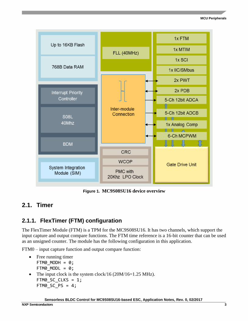
MC9S08SU16 represents very low-cost portfolio of S08 MCUs with peripherals modules dedicated for
motor control applications. The typical application segment includes BLDC sensor or sensorless motor
control applications.
The key features of the MC9S08SU16 device are as follows:
• 40-Mhz S08 core
• 768-bytes SRAM, 16-KB program flash memory
• Voltage range: 4.5 V to 18 V
• 5 V input/output for logical I/O
• One I2C module supporting SMbus communications interface
• One SCI module
• Two 12-bit ADCs with up to 8 channels
• Analog comparator with up to 4 inputs and internal 6-bit DAC
• High voltage GDU (4.5 V - 18 V)
• Two 16-bit pulse width timers (PWT)
• Two programmable delay block (PDB)
• One 16-bit FTM
• One 16-bit modulo timer (MTIM)
• One 16-bit 6-channel PWM
• Up to 17 GPIOs
• Windowed COP with multiple clock sources (watchdog)
• Inter-peripheral Crossbar Switch (XBAR)
• Cyclic redundancy check(CRC)
• Temperature range (ambient): -40°C to 105°C
Figure 1 shows the overview diagram of the MC9S08SU16 device.
MCU Peripherals
Sensorless BLDC Control for MC9S08SU16-based ESC, Application Notes, Rev. 0, 02/2017
NXP Semiconductors 3
Figure 1. MC9S08SU16 device overview
2.1. Timer
2.1.1. FlexTimer (FTM) configuration
The FlexTimer Module (FTM) is a TPM for the MC9S08SU16. It has two channels, which support the
input capture and output compare functions. The FTM time reference is a 16-bit counter that can be used
as an unsigned counter. The module has the following configuration in this application.
FTM0 – input capture function and output compare function:
Free running timer
FTM0_MODH = 0; FTM0_MODL = 0;
The input clock is the system clock/16 (20M/16=1.25 MHz).
FTM0_SC_CLKS = 1; FTM0_SC_PS = 4;

MCU Peripherals
Sensorless BLDC Control for MC9S08SU16-based ESC, Application Notes, Rev. 0, 02/2017
4 NXP Semiconductors
The FTM0CH0 is configured to the input capture function.
FTM0_C0SC = FTM0_C0SC_ELSA_MASK | FTM0_C0SC_ELSB_MASK; The FTM0CH1 is configured to the output compare function.
FTM0_C1SC = FTM0_C1SC_ELSA_MASK | FTM0_C1SC_ELSB_MASK | FTM0_C1SC_MSA_MASK;
Enable the ISR for FTM0CH0 input capture, with the priority of level 3 (the highest priority).
IPC_ILRS4_ILRn0 = 3; Enable the ISR for FTM0CH1 output compare function, with the priority of level 3 (the highest
priority).
IPC_ILRS4_ILRn1 = 3;
2.1.2. PDB0 configuration
PDB0 is used to synchronize GDU’s comparator module and PWM module. The configuration is as
follows:
The input clock is the high speed clock (40 MHz).
The single short delay mode is chosen.
PDB_CTRL0 = 0x00
2.1.3. MTIM configuration
MTIM is selected as the timer interrupt in this application and the module is configured as follows:
The timer period is configured to 3 ms (MOD_INIT = 234).
MTIM_SC |= MTIM_SC_TRST_MASK; MTIM_CLK |= MTIM_CLK_PS_MASK; MTIM_MODL = MOD_INIT&0xff; MTIM_MODH = MOD_INIT>>8;
The MTIM overflow interrupt is enabled.
MTIM_SC |= MTIM_SC_TOIE_MASK;
Enable the overflow ISR, with the priority of level 1 (low priority).
IPC_ILRS7_ILRn0 = 0;
2.1.4. PWM configuration
The PWM module is used for PWM generation which drive inverter. The module has the following
configuration:
The input clock is the high speed clock, which is 40 MHz.
The PWM fault2 interrupt and the manual fault clear functions are enabled.
PWM_FCTRLL = PWM_FCTRLL_FIE2_MASK; The output PWM frequency is set to 16 KHz (PWM_MODULO = 2500).
PWM_CMODL = PWM_MODULO%256; PWM_CMODH = PWM_MODULO/256;
The reload frequency is set to 16 KHz.
PWM_CTRLH =0;

MCU Peripherals
Sensorless BLDC Control for MC9S08SU16-based ESC, Application Notes, Rev. 0, 02/2017
NXP Semiconductors 5
The edge-aligned complementary PWM is configured to use the combined (n) and (n+1)
channels.
PWM_CNFGH = PWM_CNFGH_EDG_MASK; PWM_CNFGL = 0;
The deadtime is set to 1 us.
PWM_DTIM0L = 40; PWM_DTIM0H = 0; PWM_DTIM1L = 40; PWM_DTIM1H = 0;
The top-side polarity is negative.
PWM_CNFGH |= PWM_CNFGH_TOPNEG_MASK The reload interrupt is enabled.
PWM_CTRLL = PWM_CTRLL_PWMEN_MASK | PWM_CTRLL_PWMRIE_MASK; The LDOK feature is used to update the duty-cycle.
PWM_CTRLL |= PWM_CTRLL_LDOK_MASK; Enable PWM reload ISR, with the priority of level 2.
IPC_ILRS1_ILRn2 = 2;
2.1.5. PWT configuration
The PWT module is used to capture a pulse width and pulse period. The duty command is captured
through this module in this application. The module has the following configurations:
The input clock is set to Bus clock/128, which equals to 156.25 KHz.
PWT0_CR_PRE = 7; The PWT0IN0 (PTA6) is chosen as the PWT input port.
PWT0_CR_PINSEL = 0; The ready interrupt is disabled.
PWT0_CS_PRDYIE = 0;
2.2. Analog configuration
2.2.1. GDU configuration
The Gate Drive Unit (GDU) module is designed for power conversion and 3-phase motor control
applications. It includes high-side and low-side Field Effect Transistor (FET) pre-drivers, motor BEMF
zero crossing detection circuit, and 2-current sensing amplifiers with pre-configured 20x gain and
limitation detection. GDU is also internally connected to the Crossbar module, PWM module, and ADC
module, so the signal propagation delays can be effectively reduced or minimized. The module has the
following configurations:
The delay time needs to be added after power-on, to make sure GDU module is normal powered
before initialization.
for (delayAfterClampEnable = 20000; delayAfterClampEnable > 0; delayAfterClampEnable--); {

MCU Peripherals
Sensorless BLDC Control for MC9S08SU16-based ESC, Application Notes, Rev. 0, 02/2017
6 NXP Semiconductors
asm(nop); }
By default, the Vclamp is set to 3.84 V and it needs to be manually tuned to 5 V.
GDU_CLMPCTRL_TUNE = 4; The virtual network is enabled with the 3 internal resistors.
GDU_PHASECTRL = GDU_PHASECTRL_VNEN_MASK; The OpMAP0 is enabled for DC bus over-current protection.
GDU_CURCTRL = GDU_CURCTRL_AMP0EN_MASK; The phase detection comparator with window/filter circuit is enabled.
GDU_PHCMPxCR0 = GCMP_FILT_CNT; GDU_PHCMPxCR1 = GDU_PHCMP0CR1_EN_MASK| GDU_PHCMP0CR1_WE_MASK|GDU_PHCMP0CR1_PMODE_MASK; GDU_PHCMPxFPR = ZC_COMP_SAMP_PER_SYSU; GDU_PHCMPxCR0_HYSTCTR = 1;
Enable over-voltage ISR, with the priority of level 3 (highest priority).
IPC_ILRS1_ILRn0 = 3; Enable over-current ISR, with the priority of level 3 (highest priority).
IPC_ILRS1_ILRn1 = 3;
2.3. Others
2.3.1. Clock configuration
The internal clock source module provides clock source choices for the MCU. The module has
following configurations:
The core clock is set to 40 MHz and the bus clock to 20 MHz.
ICS_C4 = 0x00; ICS_C2 = 0x00; SIM_SCDIV = SIM_SCDIV_DIV2_MASK;
The clock gate is opened for related peripherals.
SIM_SCGC1 = SIM_SCGC1_IPC_MASK | SIM_SCGC1_DBG_MASK | SIM_SCGC1_PMC_MASK; SIM_SCGC2 = SIM_SCGC2_PDB_MASK | SIM_SCGC2_ADC0_MASK | SIM_SCGC2_GDU_CMP_MASK | SIM_SCGC2_CMP0_MASK; SIM_SCGC3 = SIM_SCGC3_FTM_MASK | SIM_SCGC3_PWT0_MASK | SIM_SCGC3_MTIM_MASK | SIM_SCGC3_PWM_MASK;
The clock trim value calibration is enabled.
ICS_C3 = 0x50;
2.3.2. XBAR configuration
This module is used as a bridge between different peripherals. The module has following configurations:

Interrupts
Sensorless BLDC Control for MC9S08SU16-based ESC, Application Notes, Rev. 0, 02/2017
NXP Semiconductors 7
The PWM reload signal is configured to sync the PDB0 module.
XBAR_SEL9 = 4; The PDB0 output is configured as GCMP compare window.
XBAR_SEL10 = 9; XBAR_SEL11 = 9;
XBAR_SEL12 = 9;
The GCMP output is configured to trigger FTM0CH0 input capture ISR.
3. Interrupts
This application has 6-interrupt services:
4 interrupts are part of the BLDC motor control algorithm.
2 interrupts are used for over-current and over-voltage protection.
Table 1 summarizes ISR numbers and priority levels.
Table 1. Interrupt service list
Source Module function Application function Vector number ISR name Priority
FTM0 Zero-crossing time Zero-crossing time 16 isr_FTMch0_inputCapture 3
FTM0 Commutation time Commutation time 17 isr_FTMch1_outputCompare 3
GDU Over current fault Over current fault 13 isr_overCurrentFault 3
GDU Over voltage fault Over voltage fault 4 isr_overVoltageFault 3
PWM PWM reload PDB register update 6 isr_PWM_reload 2
MTIM MTIM overflow Timer Event 28 isr_MTIM 1
3.1. Over-current fault interrupt
The GDU module includes the over-current protection. The related circuit description is as follows:
The current sense circuit and the over-current detection circuit are integrated in the GDU module. The
bias voltage for the current sense circuit is VREF/2, where the default VREF value is 4.2 V. Customers
can change the ADC reference voltage from 4.2 V to 5 V by setting the register of GDU_SIGBIAS.
The default amplification factor is 20. Customers can add external resistor to change the amplification
factor. For example, if 2K resistor is selected, the amplification factor is 15. If 4K resistor is selected,
the amplification factor is 12.
The over-current detection circuit is realized by the comparator. The positive input of comparator is the
output of current sense circuit, and the negative input of comparator is the output of 6-bit DAC. Figure 2
shows the over-current interrupt flow chart.
This hardware fault interrupt subroutine is used in:
6-channel PWM mask;
Setting the Fault.

Interrupts
Sensorless BLDC Control for MC9S08SU16-based ESC, Application Notes, Rev. 0, 02/2017
8 NXP Semiconductors
Isr_PWMFault2
PWM six channel mask
Set fault
RTS
Figure 2. Over-current interrupt flow chart
3.2. Over-voltage fault interrupt
The over-voltage sense circuit is integrated in the GDU module. The input of the over-voltage sense
circuit is an eighth of DC bus voltage, and the reference voltage for the over-voltage sense circuit is
divided into two classes, 22 V and 24 V. Customers can distinguish it in the over-voltage interrupt and
take corresponding measures. For details, see the SU16 reference manual. Figure 3 shows the over-
voltage interrupt flow chart.
This hardware fault interrupt subroutine is used in:
6-channel PWM mask;
Setting the Fault.

Interrupts
Sensorless BLDC Control for MC9S08SU16-based ESC, Application Notes, Rev. 0, 02/2017
NXP Semiconductors 9
Isr_overVoltageFault
PWM six channel mask
Set fault
RTS
Figure 3. Over-voltage interrupt flow chart
3.3. MTIM interrupt
The state machine is executed in this ISR every 3 ms. Figure 4 shows the MTIM interrupt flow chart.
This is periodically called and is used in the following processes:
Calculating velocityAct from periodBLDCZcFlt;
Calculating the duty ramp value;
Setting PWM duty cycle.

Interrupts
Sensorless BLDC Control for MC9S08SU16-based ESC, Application Notes, Rev. 0, 02/2017
10 NXP Semiconductors
Isr_MITM
State machine execution
RTS
Figure 4. MTIM interrupt flow chart
3.4. FTM0CH0 input capture interrupt
The zero-crossing time is captured, and the next commutation time is calculated in this interrupt service.
Figure 5 shows the FTM0CH0 input capture interrupt flow chart. This zero-crossing timer input capture
interrupt is used in the following processes:
Recording the zero-crossing time (timeBLDCZc);
Calculating the commutation period (periodBLDCZC) and filter the commutation period
(periodBLDCZcFlt);
Calculating the period (periodBLDCZcToCmt) between the zero-crossing point (timeBLDCZc)
and the sequent commutation time (timeBLDCCmt);
Calculating the sequent commutation time (timeBLDCCmt = timeBLDCZC+
periodBLDCZcToCmt).

Interrupts
Sensorless BLDC Control for MC9S08SU16-based ESC, Application Notes, Rev. 0, 02/2017
NXP Semiconductors 11
isr_FTMch0_inputCapture
Recode timeBLDCZC
Calculate periodBLDCZC
Calculate next CMT time
RTS
Figure 5. FTM0CH0 input capture interrupt flow chart
3.5. FTM0CH1 output compare interrupt
The commutation is executed in this interrupt service. Figure 6 shows the FTM0ch1 output compare
interrupt flow chart. This commutation interrupt is used in the following processes:
When ZC Detection State = Current recirculation
— Configuring XBAR_SEL4 (non-conduct phase voltage selection);
— Selecting FTM0CH0 input capture edge;
— Changing the ZC detection state;
When ZC Detection State != Current recirculation
— Calculating current recirculation period (periodBLDCZcToff);
— Calculating force commutation period (periodBLDCCmtPreSet);
— Constructing the virtual neutral point;
— Making communication according to the current sector;
— Changing the ZC detection state.

Interrupts
Sensorless BLDC Control for MC9S08SU16-based ESC, Application Notes, Rev. 0, 02/2017
12 NXP Semiconductors
isr_FTMch1_outputCompare
ZC Detection state =
current recirculation
FTMch0 input capture
enable
Preset CMT time update
XBAR configure
ZC Detection state = ZC
detection
Calculate PeriodZCtoOff
Calculate PeriodPreset
Commutation
ZC detection state =
current recirculation
Current recirculation CMT
update
RTS
Y
N
Figure 6. FTM0CH1 output compare interrupt flow chart
3.6. PWM reload interrupt
The PDB0 comparison register is updated in this ISR, as PDB’s register update has no synchronization
mechanism for MC9S08SU16.
PDB0 compare register update
When throttle calculation done = 0
Throttle calculation
When throttle calculation done != 0
dutyCycleRequestU16 calculation

Software Description
Sensorless BLDC Control for MC9S08SU16-based ESC, Application Notes, Rev. 0, 02/2017
NXP Semiconductors 13
Isr_PWM_reload
PDB comparison register updatePWTDuty calculation
Throttle calibration done?
dutyCycleRequestU16 calculation Throttle calibration
RTS
Yes
No
Figure 7. PWM reload interrupt flow chart
4. Software Description
This application core is MC9S08SU16. The low-cost S08 chip has enough peripherals and features
suitable for implementation of sensorless BLDC six-step control.
This application is written in C language using Codewarrior 10.6, and calls the S08 embedded software
library for time saving.
4.1. System concept
The concept shown in Figure 8 is chosen. The sensor-less rotor position technique developed detects the
zero-crossing points of Back-EMF induced in the motor windings. The phase Back-EMF zero-crossing
points are sensed while one of the 3-phase windings is not powered. The obtained information is
processed to commutate with the energized phase pair and to control the phase voltage with the Pulse
Width Modulation.
The neutral point voltage is reconstructed by using the internal virtual resister network, and 3
comparators are integrated in GDU peripheral. The zero-crossing detection is synchronized with the
duty cycle of the edge-aligned PWM signal by the hardware trigger using comparator’s window
function, in order to:

Software Description
Sensorless BLDC Control for MC9S08SU16-based ESC, Application Notes, Rev. 0, 02/2017
14 NXP Semiconductors
Filter high-voltage spikes produced by the switch of the MOSFETs;
Avoid detecting incorrect zero-crossing point for unipolar PWM mode.
PWM Generator with deadtime
Duty regulator
Commutation control
Zero-crossing detection
GDU
FTM0
PWT
BLDC motor
XBAR PDB0
MTIM
Dcbus currentDcbus voltgage protection
U
VW
BDM
Figure 8. Concept diagram
4.2. State machine
Figure 9 shows how this application uses the state machine to control the system flow. After resetting
the chip to configure all peripherals, the system enters never-ending loop. The state machine is executed
at 3 ms timer interrupt routine with MTIM.
• INIT
All the PWM MOSFETs are switched off and variable initialization. The state machine transits
to the STOP state.
• STOP

Software Description
Sensorless BLDC Control for MC9S08SU16-based ESC, Application Notes, Rev. 0, 02/2017
NXP Semiconductors 15
The transition to the OPENLOOP state is performed once the motor run is required.
• OPENLOOP
The motor is started-up with an initial duty cycle. The commutation period is constant and zero-
crossing detection is not executed in the first two commutation steps.
— If the zero-crossing point is not detected when the commutation step is greater than 4, the
state machine is forced to transit to the RUN state.
— If the zero-crossing point is detected when the commutation step is less than 5 and greater
than 2, the state machine transits to the RUN state.
• RUN
The motor speeds the calculation and duty cycle addition or subtraction is executed in this state.
If the motor stop is required, the state machine is switched to the STOP state.
• FAULT
— If an application detects any of the following fault:
– DC bus over voltage (Vsup > 22V)
– DC bus over current (DC bus current > 10A)
the state machine enters the FAULT state. The PWM MOSFETs are switched OFF.
— If no fault is detected in the 3 seconds period, the state machine exist the FAULT state
and transits to the INIT state.
INIT
STOP
OPENLOOP
RUN
FAULT
dutyCycleRequest >= threshold
ZC point found
| openloopCmtCnt >threshold value
faultReleaseCnt > threshold value
overCurrentFault=1
|overVoltageFault=1
overCurrentFault=1
|overVoltageFault=1
overCurrentFault=1
|overVoltageFault=1
overCurrentFault=1
|overVoltageFault=1
Throttle calibration done = 1
Figure 9. Application state machine

Software Description
Sensorless BLDC Control for MC9S08SU16-based ESC, Application Notes, Rev. 0, 02/2017
16 NXP Semiconductors
4.3. OPENLOOP
The OPENLOOP state is described as above. Figure 10 shows the startup workflow of this application.
Sector = 0
dutyCycle update
Preset CMT time
FTM0ch1 interrupt enable
ZCP detected?
Preset CMT time
expired?
Sector++
Commutation
dutyCycle update
Preset CMT time update
CMT times <2?
CMT times >4?
Yes
Yes
Yes
No
No
No
Yes
No
Openloop state
Run state
Figure 10. OOPENLOOP flow chart

Software Description
Sensorless BLDC Control for MC9S08SU16-based ESC, Application Notes, Rev. 0, 02/2017
NXP Semiconductors 17
4.4. Zero-crossing detection and commutation
Figure 11 is zero-crossing detection and commutation timing diagram. If the comparator is used to
detect zero-crossing point, the window function for comparator is used to avoid incorrect zero-crossing
point detection.
PWM TOP Channel
PDB0ch1
GCMPWindow
GCMP
XBAR_SEL9 = 4
XBAR_SEL10 = 9XBAR_SEL11 = 9XBAR_SEL12 = 9
GCMP COUT with filter
GCMP COUT without filter
Isr_FTM0InputCaptureFTM0ch0
XBAR_SEL4 = 12XBAR_SEL4 = 13XBAR_SEL4 = 14
Plus input(non-conduct phase)
Minus input(Virtual neutral)
Reload signal
1
2
3
4
Isr_FTM0OutputCompare
FTM0ch1
5
6
PWM Sync signal
PWM CNT
Isr_FTM0OutputCompare
7
8
Figure 11. Zero-crossing detection & communication timing diagram

Hardware Description
Sensorless BLDC Control for MC9S08SU16-based ESC, Application Notes, Rev. 0, 02/2017
18 NXP Semiconductors
NOTE
1. The virtual neutral can be flexibly reconstructed with the register (GDU_PHASECTRL).
2. Customers need to change the XBAR_SEL4 configuration according to sector number in the
application.
— If non-conducted phase is phase A, XBAR_SEL4 = 12.
— If non-conducted phase is phase B, XBAR_SEL4 = 13.
— If non-conducted phase is phase C, XBAR_SEL4 = 14.
3. 1 us for the PDB0 rising edge delay period in this application.
4. 12 us for the GDU comparator filter period in this application.
5. The window function is generated by PDB0ch1. The synchronization between this two
peripherals is realized by XBAR peripheral, described in Figure 11.
6. PWM and PDB0 are synchronized with the XBAR peripheral, described in Figure 11. PWM
reload signal is generated in every PWM period in this application.
7. The FTM0ch1 output compare interrupt (ZC Detection state = current recirculation) time is
obtained through calculation, not aligned to actual time points in Figure 11.
8. The FTM0ch1 output compare interrupt (ZC Detection state ≠ current recirculation) time is
obtained through calculation, not aligned to actual time points in Figure 11.
5. Hardware Description
5.1. Schematic
Figure 12 shows the CPU peripheral circuit. C1 is important and supply Vclamp to drive high bridge P-
Mosfet. C6 and C40 need to be added if customers want to use 4.2 V as ADC reference voltage.
Figure 12. MCU peripheral circuit

Hardware Description
Sensorless BLDC Control for MC9S08SU16-based ESC, Application Notes, Rev. 0, 02/2017
NXP Semiconductors 19
Figure 13 shows the 3-phase inverter and related other circuit. The amplification factor is 20x in this
application.
Figure 13. Driver circuit
5.2. Hardware board
In this application, the output current is designed for 15A. Thus the PCB layout needs to be well
considered, especially for following points:
• Heat dissipation for power components
• Power ground copper pouring to avoid influence by high frequency signal
Figure 14 shows the front side of the hardware board and Figure 15 shows the back side.
Figure 14. Front side of hardware board

Application Operation
Sensorless BLDC Control for MC9S08SU16-based ESC, Application Notes, Rev. 0, 02/2017
20 NXP Semiconductors
Figure 15. Back side of hardware board
6. Application Operation
6.1. FreeMASTER installation on PC or notebook
You can download the FreeMASTER PC application on www.NXP.com/freemaster. Select
FreeMASTER 2.0 Application Installation and click the Run button to start the installation.
6.2. Establishing connection between PC and embedded application
The FreeMASTER enables the use of multiple communication interfaces between the embedded
application and the PC or notebook (UART (RS232), CAN, Ethernet, BDM, and so on). For this
application, the BDM Communication Plug-in is used.
For the FreeMASTER configuration, follow the path:
• Project->Options->Comm

Application Operation
Sensorless BLDC Control for MC9S08SU16-based ESC, Application Notes, Rev. 0, 02/2017
NXP Semiconductors 21
Figure 16. FreeMASTER Comm page
• Project->Options->MAP Files:
Figure 17. FreeMASTER MAP Files page

Application Operation
Sensorless BLDC Control for MC9S08SU16-based ESC, Application Notes, Rev. 0, 02/2017
22 NXP Semiconductors
6.3. Application platform
Figure 18 shows the phase A voltage waveform and phase A current when the duty cycle ratio is 20%.
The purple waveform is the phase voltage, and the green waveform is the corresponding phase current
waveform.
Figure 18. Phase voltage and phase current
The motor, which is used in this application, is Tiger motor (MT2208-18). Table 2 describes motor
parameters.
Table 2. Motor parameters
Characteristics Symble Value Unit
Rated voltage V 14.8 V
Rated speed - 12000 RPM
Rated power P 109 W
Number of pole pairs PP 7
Figure 19 shows the application platform.

Revision History
Sensorless BLDC Control for MC9S08SU16-based ESC, Application Notes, Rev. 0, 02/2017
NXP Semiconductors 23
Figure 19. Application platform
6.4. Microcontroller usage
Table 3 shows how much memory is needed to run the application.
Table 3. Memory usage in Byte
Header Row Text 1 Header Row Text 2 Header Row Text 3
Flash 16 K 5222
RAM 768 2241
1. Include the stack size (78 bytes).
7. References
• MC9S08SU16 reference manual
• MC9S08SU16 datasheet
NXP documents are available at www.NXP.com.
8. Revision History Table 4. Revision history
Revision number Date Substantive changes
0 12/2016 Initial release

Document Number: AN5394 Rev. 0
02/2017
How to Reach Us:
Home Page:
nxp.com
Web Support:
nxp.com/support
Information in this document is provided solely to enable system and software
implementers to use NXP products. There are no express or implied copyright licenses
granted hereunder to design or fabricate any integrated circuits based on the
information in this document. NXP reserves the right to make changes without further
notice to any products herein.
NXP makes no warranty, representation, or guarantee regarding the suitability of its
products for any particular purpose, nor does NXP assume any liability arising out of
the application or use of any product or circuit, and specifically disclaims any and all
liability, including without limitation consequential or incidental damages. “Typical”
parameters that may be provided in NXP data sheets and/or specifications can and do
vary in different applications, and actual performance may vary over time. All operating
parameters, including “typicals,” must be validated for each customer application by
customer’s technical experts. NXP does not convey any license under its patent rights
nor the rights of others. NXP sells products pursuant to standard terms and conditions
of sale, which can be found at the following address: nxp.com/SalesTermsandConditions.
NXP™ and the NXP logo are trademarks of NXP B.V. All other product or service
names are the property of their respective owners. All rights reserved.
© 2017 NXP B.V.