seminar b topological insulators - university of...
TRANSCRIPT
�✁✂✄☎✆✝✞ ✟ ✠✡☛☞✌✡✍✎✏
✑✞✒✓✔✕☎✕✞ ✝✞ ✖✍✗✘✖✍✗✏✙✚ ✏✎ ✛✜✏✙✚
Oddelek za fiziko
Seminar 1b – 1. letnik, II. stopnja
Topological insulators
Author: Ziga Kos
Supervisor: prof. dr. Dragan Mihailovic
Ljubljana, June 24, 2013
Abstract
In the seminar, the basic ideas behind the theory of topological insulators will be presented.At first, quantum Hall and quantum spin Hall states will be explained, which show importantsimilarities to a 3-dimensional topological insulator. Symmetrical and topological properties ofthese states will be emphasised. Experimental realization of such states will be explained andthe scope for future and active research will be mentioned.
Seminar 1b – Topological insulators June 24, 2013
Contents
1 Introduction 3
2 Quantum Hall effect 42.1 Hall effect . . . . . . . . . . . . . . . . . . . . . . . . . . . . . . . . . . . . . . . . . . 42.2 Hall conductivity . . . . . . . . . . . . . . . . . . . . . . . . . . . . . . . . . . . . . . 42.3 Edge states . . . . . . . . . . . . . . . . . . . . . . . . . . . . . . . . . . . . . . . . . 6
3 Quantum spin Hall effect 73.1 Edge states protected by time reversal invariance . . . . . . . . . . . . . . . . . . . . 73.2 HgTe-CdTe quantum wells . . . . . . . . . . . . . . . . . . . . . . . . . . . . . . . . . 9
4 3D topological insulators 104.1 Experimental observations . . . . . . . . . . . . . . . . . . . . . . . . . . . . . . . . . 114.2 Applications of topological insulators . . . . . . . . . . . . . . . . . . . . . . . . . . . 12
5 Conclusion 13
2

Seminar 1b – Topological insulators June 24, 2013
1 Introduction
Usually, states of matter are recognized by which symmetry they spontaneously break. For example,translational symmetry in crystals or rotational symmetry in liquid crystals. In 1980, a new stateof matter, describing the quantum Hall effect was proposed. It does not spontaneously breakany symmetries. Instead of geometrical order, the quantum Hall state is described in terms oftopological order. Although quantum Hall effect is not the main topic of this seminar, it is included,because of a great resemblance to the quantum spin Hall effect. The generalization of quantumspin Hall effect in 3 dimensions is called a topological insulator. The main characteristic of theseeffects is that such materials are insulators in the bulk, but have surface conducting states. Theycan be described by topological quantum numbers.
Topology is a branch of mathematics that can be used to describe such properties of objectsthat do not change under continuous transformations. The most commonly used example is thetopological equivalency between a torus and a coffee mug (figure 1), since one can be continu-ously transformed into another without closing or opening any holes. Another example would bethe topology of knots (figure 1), where two knots on a closed loop are equivalent if they can betransformed one into another without cutting a string. To describe such structures, topologicalinvariants are defined.
Figure 1: a) topological equivalence between a mug and a donut, since they both have a single hole.To transform them into an orange, the hole must be closed. b) the simplest non-trivial knot – thetrefoil knot compared to the trivial closed loop – the unknot. [1],[2]
At the contact of two materials, the contact regions can exist, one with trivial topology and onewith non trivial, where the topological quantum numbers have to change between the two cases.Since topological invariants are integers, this change can not be gradual. This indicates interestingbehavior on the surface.
Two theories are generally used to describe the topological state. Topological band theorytries to evaluate topological invariants from the band structure. It is valid only for non-interactingsystems. Topological field theory takes different approach and is also valid for interacting systems.Under certain conditions, it can be reduced to topological band theory. The determination oftopological invariants is not the main topic of this seminar, but we comment on the influence thatthey have on physical systems.
3

Seminar 1b – Topological insulators June 24, 2013
2 Quantum Hall effect
2.1 Hall effect
When a conducting material is put in the magnetic field, and there is an electric current throughthe conductor, a voltage difference which is transverse to the magnetic field and the electric currentoccurs (see figure 2). This is known as Hall effect.
Figure 2: Hall effect measurement setup. [3]
The effect occurs due to the Lorentz force that separates opposite charged moving chargeson the opposite sides of the conducting plate. The value of the Hall voltage VH depends on theproperties of the conducting material, such as the density of the carrier electrons or whether amaterial is a conductor or a semiconductor. The above explanation includes electrons as particlesmoving through a conductor. It provides good evaluation of Hall voltage at room temperatures,but is invalid at extremely low temperature and high magnetic field. It these conditions we speakof quantum Hall effect. For it’s discovery, von Klitzing was awarded Nobel Prize in 1985.
2.2 Hall conductivity
In classical image, free electrons, without any momentum in direction of an external magnetic field,move in circular orbits. In quantum limit, however, the energy of these orbits is quantized inLandau levels ([1]):
εm = ~ωc(m+1
2), (1)
where ωc represents cyclotron frequency ωc = eBm . The Hall conductivity, defined as σxy = I
VHis
also quantized:
σxy = Ne2
h. (2)
N in equation 2 corresponds to the number of filled Landau levels. The degeneracy of each Landaulevel grows proportionally with the magnetic field strength ([4]), and so does the energy of eachlevel. If the strength of the magnetic field is increased, the energy of higher Landau levels may raiseabove Fermi energy. In that case, the electrons would occupy lower levels and Hall conductivitywould decrease. This is shown on figure 3 in terms of the Hall resistance, which is the inverse valueof σxy.
The way to describe this system topologically ([1]) is to introduce the Chern number. Inorder for lattice translations to commute with one other in the presence of external perpendicular
4

Seminar 1b – Topological insulators June 24, 2013
N=2
3
4
56
magnetic field (T)1 2 3 4 5 6 7
2
4
6
8
10
12
Figure 3: Hall resistance as the strength of the magnetic field gets increased. The numbers aboveplateaus show how many Landau levels are filled. [5],[6]
magnetic field, unit area enclosing a flux quantum must be defined ([1]). Only than can be stateslabeled with 2D crystal momentum ([1]). When a wave vector k is transported around Brillouinzone, Bloch wave function |u(k)〉 acquires a Berry phase, which is equal to the line integral of Berry’connection Am:
Am(k) = i〈um(k)|∇k|um(k)〉, (3)
where ∇k represents the gradient in k-space. Berry flux is defined as
Fm = ∇×Am. (4)
The Chern invariant is the integral of the Berry flux over the whole Brillouin zone:
nm =1
2π
∫d2kFm. (5)
The integration is represented graphically in figure 4. Since the surface integral of the Berry fluxis a multiple of 2π, nm is an integer. Chern number is the sum of nm over all occupied bands ([1]),
1. BZ
Figure 4: Berry flux over the Brillouin zone.
which are formed from Landau levels modified by the periodic potential:
n =∑
nm. (6)
5

Seminar 1b – Topological insulators June 24, 2013
Chern number in fact notes the number of filled Landau levels. Thouless, Kohmoto, Nightingaleand den Nijs showed, that Chern number n is identical to N in equation 2. In mathematics, Chernnumber is associated with vector bundles. In our case, we consider mapping from Brillouin zone tothe Hamiltonian in a Hilbert space. Chern number describes equivalence classes of H(k) that canbe smoothly transformed into one another ([1]).
The topological background of quantum Hall effect helps to explain why σxy is quantized sorigidly. Since the topological invariants do not change under small variation of the Hamiltonian, themeasurements of Hall conductivity can be very precise, despite of the imperfections of the material.It is of great importance in metrology. The precision of the measurement of the fine structureconstant using quantum Hall effect is just slightly below the precision of the experiment measuringthe electron’s anomalous magnetic moment ([6]). Fine structure constant is known to the precisionof 3 · 10−12, whereas the measurement involving quantum Hall effect gives the precision of 2 · 10−11
([6]).
2.3 Edge states
Quantum Hall effect takes place in two dimensions. It exhibits interesting behavior at the edgeof the sample. In a semiclassical approximation this can be explained by orbits of the electrons.In the middle of the sample, there are no restrictions for the orbits, but when electrons hit theedge, they bounce back (see figure 5). But even after collision the electron propagates in the samedirection. Since there are no states available for backscattering ([1]) this process is dissipationless.
More adequate explanation is provided by the use of topological quantum numbers. The quan-tum Hall state has non-zero Chern number, opposed to the trivial insulator with Chern number 0.A trivial insulator, without any magnetic field required, is an example of a material with Chernnumber 0. For the Chern number to change, the energy gap on the edge between two materialsmust vanish. In that case the edge states become conductive. This conductive edges are the reasonfor the perfectly quantized Hall conductivity. The exact shape of the edge is not important.
E
k
EF
0
Conduction band
Valence band
Insulator
Quantum Hall state
n=0
n=1
B
Figure 5: Electrons’ orbits in quantum Hall state. In the bulk, Fermi energy lies in the energy gap.Boundary states have no energy gap – they are conductive. Energy bands are shown in dependenceon the component of the wave vector, which is parallel to the edge.
Quantum Hall effect is the first example, how the change in topology between two bulk materialscauses special robust edge states. Another, more recent example is quantum spin Hall effect.
6
Seminar 1b – Topological insulators June 24, 2013
3 Quantum spin Hall effect
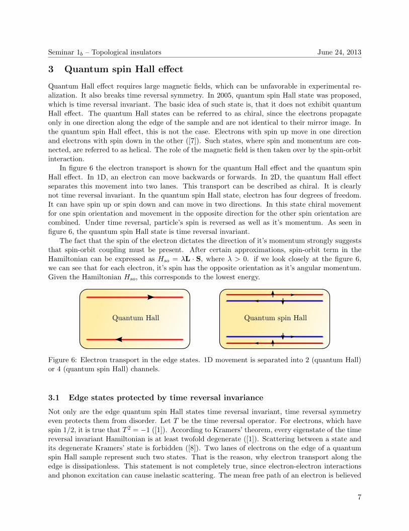
Quantum Hall effect requires large magnetic fields, which can be unfavorable in experimental re-alization. It also breaks time reversal symmetry. In 2005, quantum spin Hall state was proposed,which is time reversal invariant. The basic idea of such state is, that it does not exhibit quantumHall effect. The quantum Hall states can be referred to as chiral, since the electrons propagateonly in one direction along the edge of the sample and are not identical to their mirror image. Inthe quantum spin Hall effect, this is not the case. Electrons with spin up move in one directionand electrons with spin down in the other ([7]). Such states, where spin and momentum are con-nected, are referred to as helical. The role of the magnetic field is then taken over by the spin-orbitinteraction.
In figure 6 the electron transport is shown for the quantum Hall effect and the quantum spinHall effect. In 1D, an electron can move backwards or forwards. In 2D, the quantum Hall effectseparates this movement into two lanes. This transport can be described as chiral. It is clearlynot time reversal invariant. In the quantum spin Hall state, electron has four degrees of freedom.It can have spin up or spin down and can move in two directions. In this state chiral movementfor one spin orientation and movement in the opposite direction for the other spin orientation arecombined. Under time reversal, particle’s spin is reversed as well as it’s momentum. As seen infigure 6, the quantum spin Hall state is time reversal invariant.
The fact that the spin of the electron dictates the direction of it’s momentum strongly suggeststhat spin-orbit coupling must be present. After certain approximations, spin-orbit term in theHamiltonian can be expressed as Hso = λL · S, where λ > 0. if we look closely at the figure 6,we can see that for each electron, it’s spin has the opposite orientation as it’s angular momentum.Given the Hamiltonian Hso, this corresponds to the lowest energy.
Quantum Hall Quantum spin Hall
Figure 6: Electron transport in the edge states. 1D movement is separated into 2 (quantum Hall)or 4 (quantum spin Hall) channels.
3.1 Edge states protected by time reversal invariance
Not only are the edge quantum spin Hall states time reversal invariant, time reversal symmetryeven protects them from disorder. Let T be the time reversal operator. For electrons, which havespin 1/2, it is true that T 2 = −1 ([1]). According to Kramers’ theorem, every eigenstate of the timereversal invariant Hamiltonian is at least twofold degenerate ([1]). Scattering between a state andits degenerate Kramers’ state is forbidden ([8]). Two lanes of electrons on the edge of a quantumspin Hall sample represent such two states. That is the reason, why electron transport along theedge is dissipationless. This statement is not completely true, since electron-electron interactionsand phonon excitation can cause inelastic scattering. The mean free path of an electron is believed
7

Seminar 1b – Topological insulators June 24, 2013
to be of the order of few microns at low temperatures ([9]). Transport experiments (Hall resistancemeasurements) on HgTe quantum wells are performed at temperature below 30 mK on distances offew µm ([10]).
The absence of the elastic scattering can be explained by a semiclassical example as well. Onthe edge, there are only two states. Dissipation can occour only from one state to another. Thereare two possibilities of this, represented on the figure 7. On the left example, electron’s spin rotatesclockwise by the angle of π and on the right example by the angle of −π. On rotation of 2π, which isexactly the difference between two cases here, an electron’s wave function acquires additional factorof −1. Therefore, both states interfere destructively and backscattering is not allowed. This holdsif the impurity around which an electron would backscatter is non-magnetic. Magnetic impuritywould break time reversal symmetry and the electron transport would no longer be dissipationless.
Figure 7: Two possibilities of scattering around impurity. If impurity is non-magnetic both interferedestructively with one another. [8]
In time reversal invariant systems, the Chern number is always zero ([1]). Additional topologicalinvariant must be defined to describe the topological states of such systems. A new invariant isZ2 invariant, which means it can have only 0 or 1 values ([1]). Due to Kramers’ theorem, edgestate dispersions must cross where k = −k, that is at k = 0 and k = π/a ([1]) – at the edgeof the Brilloiun zone. The dispersion lines can cross Fermi energy even or odd number of times,which is represented in figure 8. An even number of crossing can be eliminated by slight changes ofdispersion. On the other hand, an odd number of crossings can not be eliminated. That is the caseof topologically nontrivial insulator. This even or odd difference is the reason for the Z2 invariant.
E
EF
0 k
Conduction band
Valence band
E
EF
0 k
Conduction band
Valence band
Figure 8: Dispersion of 1D edge states intersects Fermi energy even or odd number of times, whichleads to topologically trivial (even times) or nontrivial (odd) states. k represents a projection of2D Brillouin zone on the axis parallel to the edge. [9]
8
Seminar 1b – Topological insulators June 24, 2013
3.2 HgTe-CdTe quantum wells
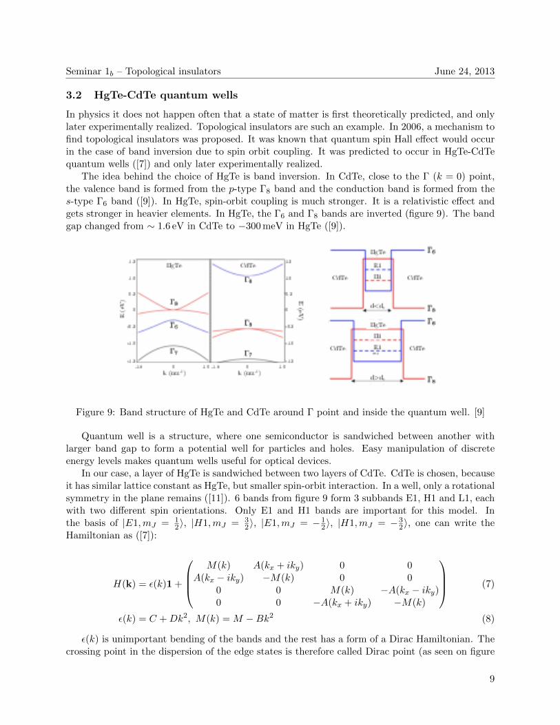
In physics it does not happen often that a state of matter is first theoretically predicted, and onlylater experimentally realized. Topological insulators are such an example. In 2006, a mechanism tofind topological insulators was proposed. It was known that quantum spin Hall effect would occurin the case of band inversion due to spin orbit coupling. It was predicted to occur in HgTe-CdTequantum wells ([7]) and only later experimentally realized.
The idea behind the choice of HgTe is band inversion. In CdTe, close to the Γ (k = 0) point,the valence band is formed from the p-type Γ8 band and the conduction band is formed from thes-type Γ6 band ([9]). In HgTe, spin-orbit coupling is much stronger. It is a relativistic effect andgets stronger in heavier elements. In HgTe, the Γ6 and Γ8 bands are inverted (figure 9). The bandgap changed from ∼ 1.6 eV in CdTe to −300 meV in HgTe ([9]).
Figure 9: Band structure of HgTe and CdTe around Γ point and inside the quantum well. [9]
Quantum well is a structure, where one semiconductor is sandwiched between another withlarger band gap to form a potential well for particles and holes. Easy manipulation of discreteenergy levels makes quantum wells useful for optical devices.
In our case, a layer of HgTe is sandwiched between two layers of CdTe. CdTe is chosen, becauseit has similar lattice constant as HgTe, but smaller spin-orbit interaction. In a well, only a rotationalsymmetry in the plane remains ([11]). 6 bands from figure 9 form 3 subbands E1, H1 and L1, eachwith two different spin orientations. Only E1 and H1 bands are important for this model. Inthe basis of |E1,mJ = 1
2〉, |H1,mJ = 32〉, |E1,mJ = −1
2〉, |H1,mJ = −32〉, one can write the
Hamiltonian as ([7]):
H(k) = ε(k)1 +
M(k) A(kx + iky) 0 0
A(kx − iky) −M(k) 0 00 0 M(k) −A(kx − iky)0 0 −A(kx + iky) −M(k)
(7)
ε(k) = C +Dk2, M(k) = M −Bk2 (8)
ε(k) is unimportant bending of the bands and the rest has a form of a Dirac Hamiltonian. Thecrossing point in the dispersion of the edge states is therefore called Dirac point (as seen on figure
9
Seminar 1b – Topological insulators June 24, 2013
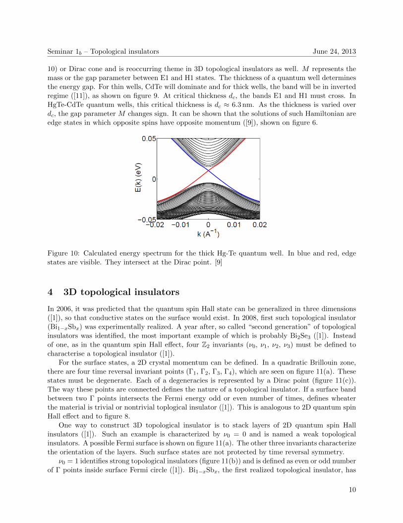
10) or Dirac cone and is reoccurring theme in 3D topological insulators as well. M represents themass or the gap parameter between E1 and H1 states. The thickness of a quantum well determinesthe energy gap. For thin wells, CdTe will dominate and for thick wells, the band will be in invertedregime ([11]), as shown on figure 9. At critical thickness dc, the bands E1 and H1 must cross. InHgTe-CdTe quantum wells, this critical thickness is dc ≈ 6.3 nm. As the thickness is varied overdc, the gap parameter M changes sign. It can be shown that the solutions of such Hamiltonian areedge states in which opposite spins have opposite momentum ([9]), shown on figure 6.
Figure 10: Calculated energy spectrum for the thick Hg-Te quantum well. In blue and red, edgestates are visible. They intersect at the Dirac point. [9]
4 3D topological insulators
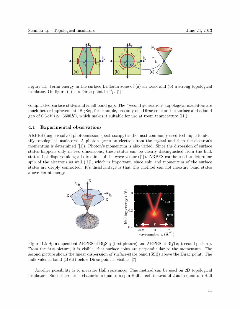
In 2006, it was predicted that the quantum spin Hall state can be generalized in three dimensions([1]), so that conductive states on the surface would exist. In 2008, first such topological insulator(Bi1−xSbx) was experimentally realized. A year after, so called “second generation” of topologicalinsulators was identified, the most important example of which is probably Bi2Se3 ([1]). Insteadof one, as in the quantum spin Hall effect, four Z2 invariants (ν0, ν1, ν2, ν3) must be defined tocharacterise a topological insulator ([1]).
For the surface states, a 2D crystal momentum can be defined. In a quadratic Brillouin zone,there are four time reversal invariant points (Γ1, Γ2, Γ3, Γ4), which are seen on figure 11(a). Thesestates must be degenerate. Each of a degeneracies is represented by a Dirac point (figure 11(c)).The way these points are connected defines the nature of a topological insulator. If a surface bandbetween two Γ points intersects the Fermi energy odd or even number of times, defines wheaterthe material is trivial or nontrivial toplogical insulator ([1]). This is analogous to 2D quantum spinHall effect and to figure 8.
One way to construct 3D topological insulator is to stack layers of 2D quantum spin Hallinsulators ([1]). Such an example is characterized by ν0 = 0 and is named a weak topologicalinsulators. A possible Fermi surface is shown on figure 11(a). The other three invariants characterizethe orientation of the layers. Such surface states are not protected by time reversal symmetry.
ν0 = 1 identifies strong topological insulators (figure 11(b)) and is defined as even or odd numberof Γ points inside surface Fermi circle ([1]). Bi1−xSbx, the first realized topological insulator, has
10
Seminar 1b – Topological insulators June 24, 2013
Figure 11: Fermi energy in the surface Brilloiun zone of (a) an weak and (b) a strong topologicalinsulator. On figure (c) is a Dirac point in Γ1. [1]
complicated surface states and small band gap. The “second generation” topological insulators aremuch better improvement. Bi2Se3, for example, has only one Dirac cone on the surface and a bandgap of 0.3 eV (kb · 3600K), which makes it suitable for use at room temperature ([1]).
4.1 Experimental observations
ARPES (angle resolved photoemission spectroscopy) is the most commonly used technique to iden-tify topological insulators. A photon ejects an electron from the crystal and then the electron’smomentum is determined ([1]). Photon’s momentum is also varied. Since the dispersion of surfacestates happens only in two dimensions, these states can be clearly distinguished from the bulkstates that disperse along all directions of the wave vector ([1]). ARPES can be used to determinespin of the electrons as well ([1]), which is important, since spin and momentum of the surfacestates are deeply connected. It’s disadvantage is that this method can not measure band statesabove Fermi energy.
ky
kx
K
E
K
-0.2 0 0.2
0
0.2
0.4
Figure 12: Spin dependent ARPES of Bi2Se3 (first picture) and ARPES of Bi2Te3 (second picture).From the first picture, it is visible, that surface spins are perpendicular to the momentum. Thesecond picture shows the linear disperssion of surface-state band (SSB) above the Dirac point. Thebulk-valence band (BVB) below Dirac point is visible. [7]
Another possibility is to measure Hall resistance. This method can be used on 2D topologicalinsulators. Since there are 4 channels in quantum spin Hall effect, instead of 2 as in quantum Hall
11

Seminar 1b – Topological insulators June 24, 2013
effect, resistance is quantized with the base level of h/2e2. Figure 13 shows the measurement ofresistance with respect to gate voltage for different thicknesses of the HgTe quantum well. Whenthe thickness of the HgTe layer is beyond dc, system behaves as an insulator (left picture). On theright picture are the measurements for d > dc and the width of the samples is varied. They allshow the same quantization of h/2e2 at small enough voltages. This proves edge conducting states.
gate voltage gate voltage
Figure 13: Measured Hall resistance on HgTe quantum wells for d < dc (left picture) and d > dc(right picture). Three different curves present measurements for three different sample widths.Since they all reach the plateau at h
2e , this proves edge states. [7]
Besides already mentioned methods, the surface Hall conductivity can also be observed byoptical methods or by measuring the magnetic fields, induced by the surface currents ([1]). Anotherpossibility is the use of scanning tunneling microscopy, which can provide additional informationabout impurities or the edges on the surface ([9]).
4.2 Applications of topological insulators
With the use of topological insulators, some interesting quasiparticles can be created, that areotherwise very elusive. Such example would be Marjorana fermions. They can be created bycombining topological insulators with superconductors. Majorana fermions are particles which arealso their antiparticles. They are of great importance for quantum computing. Seperated pairof Majorana bound states represents a qubit ([1]). Quantum information would be topologicallyprotected. Exchanging Marjorana states creates non-Abelian statistic, meaning that the stateof the system depends on the order in which the exchange was performed ([12]). Because ofthese properties, Marjorana states would be an important building block of a topological quantumcomputer.
12

Seminar 1b – Topological insulators June 24, 2013
5 Conclusion
Topological insulators are new and exiting field of physics, that has evolved in the last decade.They are a great achievement for the theoretical physics, since their existence was first predictedby theoretical approach. The classification of insulators into topological classes has proven to be anpowerful approach and can be extended to topological superconductors. Besides topological super-conductors, the main theoretical challenges for the future are believed to be electron-electron in-teractions, disorder effects and fractional topological insulators ([9]). For the experimental physics,the challenges include the production of pure enough materials, that are completely insulating inthe bulk, to tune Fermi level close to the Dirac point and to detect exotic quasiparticles ([9]).
As explained in the seminar, topological insulators are a playground to produce and to exper-iment with many quaiparticles, some of them have not been previously produced anywhere else.The proximity effect of superconductors can produce Majorana fermions. These could be the basisof the topological quantum computers. Dissipationless channels in quantum spin Hall states couldbe used for their low power consumption. Topological insulators have the potential for spintronicsdevices, infrared detectors and thermoelectric applications ([9]). The field has extended way abovethe initial expectations and certainly holds many new interesting developments in the future.
13

Seminar 1b – Topological insulators June 24, 2013
References
[1] M. Z. Hasan and C. L. Kane, Rev. Mod. Phys. 82 3045 (2010)
[2] J. E. Moore, Nature 464 194 (2010)
[3] http://en.wikipedia.org/wiki/Hall effect, (available on May 7, 2013)
[4] http://en.wikipedia.org/wiki/Quantum hall effect, (available on May 26, 2013)
[5] M. A. Paalanen et al, Phys. Rev. B 25 5566 (1982)
[6] J. E. Avron et al, Phys. Today 58 38 (2003)
[7] X. L. Qi and S. C. Zhang, Phys. Today 63 33 (2010)
[8] J. Maciejko et al, Annu. Rev. Condens. Matter Phys. 2 31 (2011)
[9] X. L. Qi and S. C. Zhang, Rev. Mod. Phys. 83 1057 (2011)
[10] M. Konig et al, J. Phys. Soc. Jpn 77 031007 (2008)
[11] B. A. Bernevik et al, Science 314 1757 (2006)
[12] http://en.wikipedia.org/wiki/Majorana fermion, (available on May 22, 2013)
[13] R. Li et al, Nature Phys. 6 284 (2010)
14