semiconductor memories lecture 1: may 10, 2006 ee summer camp abhinav agarwal
TRANSCRIPT

Semiconductor Memories
Lecture 1: May 10, 2006EE Summer CampAbhinav Agarwal

Outline
Concept/need of memory Parameters Types/classification Basic features Basic Cell circuits Peripheral circuitry
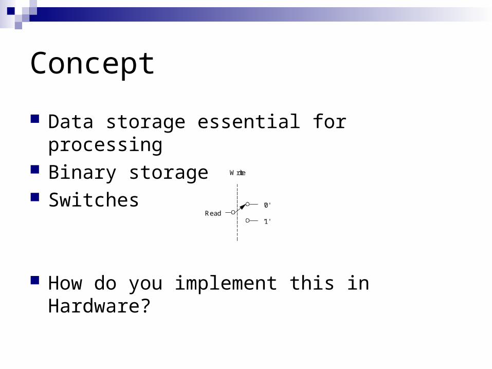
Concept
Data storage essential for processing Binary storage Switches
How do you implement this in Hardware?
'0'
'1'Read
Write

Requirements
Easy reading Easy Writing High density Speed, more speed and still more speed

Memory Chip Configuration
Ro
w D
ec
Memory Cell Array
Row AddressN bits
Complete AddressN+M Bits
2M Cells
Din
Dout
I/O Controldin
dout
Column Dec.
2N Cells
WL
DL
Cell
ControlSignals
I/O Inte
rfaceColumn Address
M Bits
© Digital Integrated Circuits2nd Memories
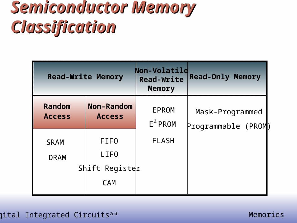
Semiconductor Memory ClassificationSemiconductor Memory Classification
Read-Write MemoryNon-VolatileRead-Write
Memory
Read-Only Memory
EPROM
E2PROM
FLASH
RandomAccess
Non-RandomAccess
SRAM
DRAM
Mask-Programmed
Programmable (PROM)
FIFO
Shift Register
CAM
LIFO

RAM
Random write and read operation for any cell Volatile data Most of computer memory DRAM
Low Cost High Density Medium Speed
SRAM High Speed Ease of use Medium Cost

ROM
Non-volatile Data Method of Data Writing Mask ROM
Data written during chip fabrication
PROM Fuse ROM: Non-rewritable EPROM: Erase data by UV rays EEPROM: Erase and write through electrical means
Speed 2-3 times slower than RAM Upper limit on write operations Flash Memory – High density, Low Cost

Basic Cells
DRAM
WL
DL
SRAM
VDD
WLWL
DLDL

© Digital Integrated Circuits2nd Memories
Static CAM Memory CellStatic CAM Memory Cell
CAM
Bit
Word
Bit
••• CAM
Bit Bit
CAM
Word
Wired-NOR Match Line
Match M1
M2
M7M6
M4 M5M8 M9
M3int
SWord
••• CAM
Bit Bit
S

© Digital Integrated Circuits2nd Memories
CAM in Cache MemoryCAM in Cache Memory
CAM
ARRAY
Input Drivers
Tag HitAddress
SRAM
ARRAY
Sense Amps / Input Drivers
DataR/W

ROM
Fuse ROM EEPROM
WL
DL
WL
DL
Floating Gate
© Digital Integrated Circuits2nd Memories
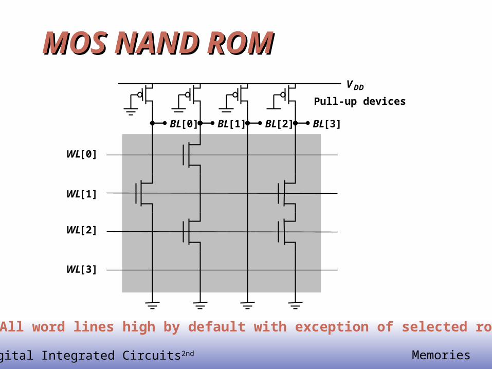
MOS NAND ROMMOS NAND ROM
All word lines high by default with exception of selected row
WL [0]
WL [1]
WL [2]
WL [3]
VDD
Pull-up devices
BL[3]BL [2]BL [1]BL [0]

© Digital Integrated Circuits2nd Memories
Non-Volatile MemoriesNon-Volatile MemoriesThe Floating-gate transistor (FAMOS)The Floating-gate transistor (FAMOS)
Floating gate
Source
Substrate
Gate
Drain
n+ n+_p
tox
tox
Device cross-section Schematic symbol
G
S
D

© Digital Integrated Circuits2nd Memories
Floating-Gate Transistor ProgrammingFloating-Gate Transistor Programming
0 V
-5 V 0 V
DS
Removing programming voltage leaves charge trapped
5 V
-2.5 V 5 V
DS
Programming results in higher VT.
20 V
10 V 5 V 20 V
DS
Avalanche injection

© Digital Integrated Circuits2nd Memories
A “Programmable-Threshold” TransistorA “Programmable-Threshold” Transistor
“0”-state “1”-state
DVT
VWL VGS
“ON”
“OFF”
© Digital Integrated Circuits2nd Memories
PeripheryPeriphery
Decoders Sense Amplifiers Input/Output Buffers Control / Timing Circuitry
© Digital Integrated Circuits2nd Memories
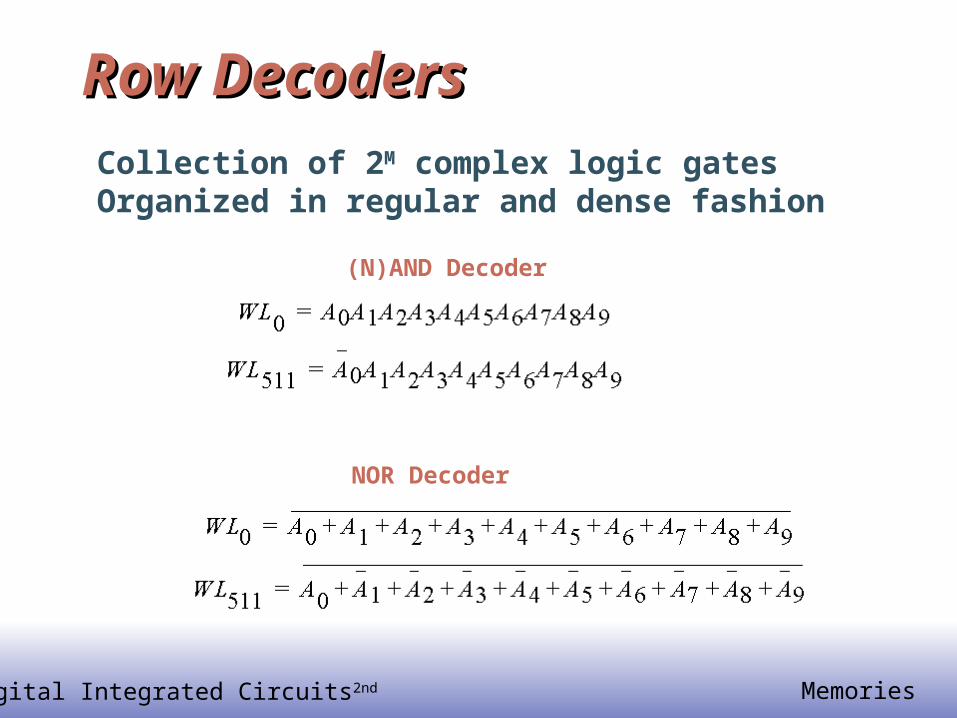
Row DecodersRow DecodersCollection of 2M complex logic gatesOrganized in regular and dense fashion
(N)AND Decoder
NOR Decoder

© Digital Integrated Circuits2nd Memories
Hierarchical DecodersHierarchical Decoders
• • •
• • •
A2A2
A2A3
WL 0
A2A3A2A3A2A3
A3 A3A0A0
A0A1A0A1A0A1A0A1
A1 A1
WL 1
Multi-stage implementation improves performance
NAND decoder usingNAND decoder using2-input pre-decoders2-input pre-decoders

© Digital Integrated Circuits2nd Memories
Sense AmplifiersSense Amplifiers
tpC V
Iav----------------=
make V as smallas possible
smalllarge
Idea: Use Sense Amplifer
outputinput
s.a.smalltransition

© Digital Integrated Circuits2nd Memories
Sense Amp OperationSense Amp Operation
DV(1)
V(1)
V(0)
t
VPRE
VBL
Sense amp activatedWord line activated
© Digital Integrated Circuits2nd Memories
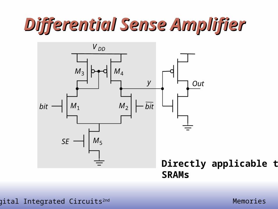
Differential Sense AmplifierDifferential Sense Amplifier
Directly applicable toSRAMs
M4
M1
M5
M3
M2
VDD
bitbit
SE
Outy

© Digital Integrated Circuits2nd Memories
Reliability and YieldReliability and Yield

References
Digital Integrated Circuits, 2nd Edition, Jan Rabaey, Anantha Chandrakasan, Borivoje Nikolic
Chapter 12 http://bwrc.eecs.berkeley.edu/IcBook/slides.htm
Sedra & Smith, Microelectronic Circuits, 4th Edition, Chapter 13 Section 13.9, 13.10, 13.11, 13.12
VLSI Memory Chip Design, Kiyoo Itoh