self report - info.ifpan.edu.pl
TRANSCRIPT

Załącznik 3 Self report English version – Rafał Jakieła
1
Warsaw, February 7, 2020
Dr Rafał Jakieła
Laboratory of X-Ray and Electron Microscopy Research
Group of X-ray Spectroscopy and Microanalysis
Institute of Physics Polish Academy of Sciences
Al. Lotników 32/46, 02-668 Warszawa
e-mail: [email protected]
SELF REPORT
1. Personal data: ...................................................................................................................... 2
2. Education and Degrees........................................................................................................ 2
3. Information on Previous Employment ................................................................................ 2
4. Description of the achievements, set out in art. 219 para 1 point 2 of the Act ................... 3
5. Scientific achievement being the subject of habilitation .................................................... 5
6. Bibliometric information .................................................................................................. 23
6.1 Total Number of Publications .................................................................................... 23
6.2 Total Impact Factor of publications ........................................................................... 23
6.3 Total citation number of publication ......................................................................... 23
6.4 Hirsch Index of publication ....................................................................................... 23
7. Presentation of significant scientific activity carried out at more than one university,
scientific or cultural institution, especially at foreign institutions. .......................................... 24
7.1 Scientific work before obtaining a Ph. D. degree in physics ..................................... 24
7.2 Scientific work after obtaining a Ph. D. degree in physics ........................................ 26
8. Presentation of teaching and organizational achievements as well as achievements in
popularization of science or art. ............................................................................................... 31
8.1 Creative professional works: ..................................................................................... 31
8.2 Managing and Participation in Domestic or International Research Projects before
obtaining Ph.D. degree ......................................................................................................... 32
8.3 Managing and Participation in Domestic or International Research Projects after
obtaining Ph.D. degree ......................................................................................................... 32
8.4 List of invited papers delivered at national or international conferences: ................. 33
8.5 Other papers personally delivered at national or international conferences: ............. 33
8.6 Seminars presented: ................................................................................................... 34
8.7 Construction of a unique science equipment ............................................................. 34
8.8 Organization of conferences, reviewing and editorial activities ............................... 34
8.9 Didactics and popularization of science .................................................................... 35
8.10 Patents and patent applications .................................................................................. 35
9. Bibliography ..................................................................................................................... 36

Załącznik 3 Self report English version – Rafał Jakieła
2
1. Personal data:
Rafał Jakieła
Born: April 20, 1974 in Rzeszow
Address: ul. Zadumana 1A/105, 02-206 Warszawa
2. Education and Degrees
Ph. D. in Physics 2005 Institute of Physics, Polish Academy of Sciences
Specialization: Solid State Physics
Thesis topic: Diffusion Mechanisms in A3B5 semiconductors
Ph. D. advisor: prof. dr hab. Adam Barcz
M. Sc. in Physics 1999 College of Sciences in Warsaw
Specialization: Physical Measuring Apparatus
Thesis topic: Silicon implantation into GaAs
M. Sc. degree advisor: prof. dr hab. Adam Barcz
Bachelor degree1997 College of Sciences in Warsaw
Specialization: Physics, Mathematics and Chemistry with a
Specialty in Electronic Measuring Equipment
Secondary education 1994 Electronic Technical School in Rzeszow
Specialization: Electrical and electronic industrial automation
3. Information on Previous Employment
01/07/2005 – now Specialist, Institute of Physics, Polish Academy of Sciences
Studies of semiconductor structures and materials using the SIMS
method
01/09/2006 – now IT administrator, Primary School 389 in Warsaw
30/09/1998 – 31/06/2005 Ph. D. student, Institute of Physics, Polish Academy of Sciences
01/11/1998 – 31/12/2015 Assistant, Institute of Electronic Materials Technology
Studies of semiconductor grown by MOCVD epitaxy.
01/05/1998 – 31/12/1998 Programmer, Computer Service Matrix sp. z o.o.

Załącznik 3 Self report English version – Rafał Jakieła
3
4. Description of the achievements, set out in art. 219 para 1 point 2 of the Act
Subject of publications: The role of atmospheric elements in the semiconductors
H1 R. Jakiela, E. Dumiszewska, P. Caban, A. Stonert, A. Turos, A. Barcz – Oxygen
diffusion into GaN from oxygen implanted GaN or Al2O3 – Phys. Status Solidi C 8
(2011) 1513
(IF = 0, cit. 7)
My contribution to this publication consisted of the idea and preparation of whole
experiment, preparing of MOCVD grown sample for implantation and annealing,
performing of all SIMS measurements as well as processing the obtained results.
I estimate my contribution to the 70%.
H2 A. Barcz, M. Kozubal, R. Jakieła, J. Ratajczak, J. Dyczewski, K. Gołaszewska, T.
Wojciechowski, G. K. Celler – Diffusion and impurity segregation in hydrogen-
implanted silicon carbide – Journal of Applied Physics 115 (2014) 223710
(IF = 2.183, cit. 11)
My contribution to this publication consisted of performing of all SIMS measurements,
processing the obtained results and participation in editing the manuscript. I estimate
my contribution to the 40%.
H3 A. Barcz, R. Jakieła, M. Kozubal, J. Dyczewski, G.K. Celler – Incorporation of oxygen
in SiC implanted with hydrogen – Nuclear Instruments and Methods in Physics Research
B 365 (2015) 146
(IF = 1.389, cit. 2)
My contribution to this publication consisted of performing of all SIMS measurements,
processing the obtained results and participation in editing the manuscript. I estimate
my contribution to the 40%
H4 R. Czernecki, E. Grzanka, R. Jakiela, S. Grzanka, C. Skierbiszewski, H. Turski, P.
Perlin, T. Suski, K. Donimirski, M. Leszczynski – Hydrogen diffusion in GaN:Mg and
GaN:Si – Journal of Alloys and Compounds 747 (2018) 354
(IF = 4.175, cit. 5)

Załącznik 3 Self report English version – Rafał Jakieła
4
My contribution to this publication consisted of performing of all SIMS measurements,
processing the obtained results and participation in editing the manuscript. I estimate
my contribution to the 40%
H5 R. Jakiela, A. Barcz, J. Sarnecki, G. K. Celler – Ultrahigh sensitivity SIMS analysis of
oxygen in silicon – Surface and Interface Analysis 50 (2018) 729
(IF = 1.319, cit. 3)
The above article is a summary of over 10-years research on oxygen diffusion in silicon.
My contribution to this publication consisted of carrying out all SIMS measurements,
writing a FTCS diffusion simulation program (Forward Time Center Space), comparing
the SIMS results with the results obtained from the simulation and co-editing the
manuscript. I estimate my contribution to the 80%
H6 R. Jakieła – The role of atmospheric elements in the wide band-gap semiconductors –
Acta Physica Polonica A 136(6) (2019) 916
(IF = 0.545, cit. 0)
The above article is a summary of my over 20-years’ experience in the measurement of
dopants and impurities in wide-band semiconductors, i.e. GaN, ZnO and SiC, in which
atmospheric elements, i.e. H, C, N and O, played a key role. The article is divided into
4 chapters (one for each element) including a summary of the current state of art on the
properties of the element in the given semiconductor and original results aimed at
showing the measurement methodology of a given element by the SIMS method with
an emphasis on its detectability. The idea, measurement, writing and editing the whole
manuscript is 100% of my contribution.
Total number of citations, excluding autocitation - 23.
Statements of co-authors of publications, confirming them individual contributions to the
paper are attached in attachment 5.

Załącznik 3 Self report English version – Rafał Jakieła
5
5. Scientific achievement being the subject of habilitation
5.1 Introduction
Since the beginning of the establishment of the Secondary Ion Mass Spectrometry (SIMS)
laboratory at the Institute of Physics Polish Academy of Sciences, I have participated in the
development and improvement of this complex analytical method and its applications for
semiconductor studying. As a result of developing special procedures and spectrometer
configuration, it was possible to obtain detection sensitivity for elements such as H, C, N, O,
especially demanding due to their prevalence - at a level unattainable for most laboratories in
the world [H5]. This fact somehow determined the main scope of my research and, as a
consequence, the subject of my habilitation thesis.
All chemical processes taking place in the Earth's atmosphere are inevitably exposed to
contamination with its gaseous components. Therefore, the main elements of the Earth's
atmosphere, i.e. hydrogen (H), carbon (C), nitrogen (N) and oxygen (O), can be included in
matter either as the main components or as trace contaminants. The same applies to
semiconductor materials where they are either the main component of some semiconductors
like GaN, ZnO, SiC, or intentional dopant like C in GaN, or N in ZnO and SiC. They present a
common source of contamination in processes occurring at atmospheric pressure, but also those
carried out under high vacuum, by interacting with residual gases. For many semiconductor
material growth processes, these elements are inert gases, but very often have a dominant effect
on their electrical properties. They can introduce donor or acceptor carriers into the material, or
cause passivation of carriers in a semiconductors.
On the other hand, the widespread occurrence of atmospheric gases imposes a limit of
detection when measuring their concentration in semiconductors, depending on the degree of
their adsorption on the surface of the sample. Most quantitative analytical methods are not well
adapted to measuring the content of these elements in solids, among others due to the high
contribution of the environment to the useful signal. The secondary ion mass spectrometry
method, operating in ultra-high vacuum and using the ionization facility of atmospheric
elements, allows, as one of the few methods, to measure their concentration in materials at a
ppm level or lower. It also gives the opportunity to determine their depth distribution into the
sample. This allows studying the properties of such dopants in semiconductors, i.e. their
diffusion and segregation coefficients, or formation energies related to the solubility of a given
dopant in a semiconductor.

Załącznik 3 Self report English version – Rafał Jakieła
6
5.2 Oxygen properties in gallium nitride [H1]
Oxygen is the second abundant atmospheric element and constitutes over 20% of the Earth's
atmosphere, and moreover ~ 46% of the Earth's crust and ~ 61% of the human body. It is also
the most reactive element contained in the atmosphere, easily forming chemical compounds
with the majority of elements. The high oxygen reactivity is due to its electron configuration.
The two unpaired electrons of the O2 molecule make it highly susceptible to bond formation.
Oxygen occurs in two allotropic forms: (oxygen – O2 and ozone – O3), both are excellent
oxidants. Usually, oxygen is present in the oxidation state –2 in the O2- form, but it can also
form other ions, e.g. O22- or O2
–. For various possible oxidation states, many molecular
compounds can be formed when another element reacts with oxygen.
In material engineering, oxygen is an issue mainly in III-V semiconductors, where in most cases
act as a donor. A high oxygen content occurs in semiconductors containing elements very easily
reacting with oxygen, i.e. Al in AlGaN and AlGaAs or Mn in MnGaAs and MnGaN.
The oxygen in GaN very easily substitutes the nitrogen site creating donor state ON, due to the
similar size of atoms. Therefore, nominally undoped GaN exhibits an n-type. The first report
on the growth of GaN crystals stated that it is defects that are responsible for the high electron
conductivity of the material, mainly the nitrogen vacancy VN. This hypothesis has been
questioned by Seifert [1], showing more likely oxygen contamination. By removing oxygen
from ammonia used for crystal growth and using Mg3N2, significant reduction of electron
concentration in GaN crystals was achieved. More comprehensive research on the oxygen in
the GaN layers obtained by the MOCVD method was performed by Chung and Gershenzon
[2]. The increase of carrier concentration along with an increase of oxygen concentration was
observed and the energy level of ON donor amounting to 78 meV was determined by means of
luminescence measurements. In the oxygen-implanted GaN the ionization energy (~29 meV)
of oxygen dopant by means of electrical measurements was determined [3]. Moreover, the low
activation efficiency of ON was observed. From the redistribution of oxygen implanted into
GaN, the upper limit of the oxygen diffusion coefficient at the level of 2.7×10⁻¹³ cm2/s at the
temperature of 1125°C was determined. Low diffusion coefficient of oxygen was confirmed in
SiO2/GaN samples [4].
The oxygen concentration in GaN depends on the conditions of material growth [5]. MBE or
MOCVD growth technology allows to obtain clean enough samples that the level of oxygen
concentration is below the detection limit of the SIMS method (<1016 at/cm3) [H6]. Equally

Załącznik 3 Self report English version – Rafał Jakieła
7
low oxygen concentration was also achieved in crystals grown by hydride vapor phase epitaxy
(HVPE), which makes it possible to obtain layers of even hundreds of microns thick [6, 7].
Bulk crystals growth methods such as high-pressure method [8], ammonothermal method [9]
or more and more popular Na-flux method, unfortunately not yet achieved such crystal purity
in terms of oxygen content [10, 11]. The greatest purity in this respect was achieved in Na-flux
method where the oxygen concentration has been reduced to a level of ~3×10¹⁶ at/cm3. In the
ammonothermal and high-pressure methods, the oxygen concentration exhibits values
respectively >1018 at/cm3 and >1019 at/cm3.
In the paper [H1] I focused on the high oxygen content in the GaN layer adjacent to the sapphire
substrate, often observed in measurements of GaN layers deposited on Al2O3 by various
epitaxial methods. The aim of the study was to check if the extent oxygen that builds up in the
semiconductor during the growth of GaN layers is oxygen from sapphire or extent oxygen
adsorbed on the substrate is the result of improper substrate preparation for the epitaxy process.
For this reason, I wrote a research project to the SPIRIT consortium and I was able to visit the
Helmholtz-Zentrum Dresden-Rossendorf Ev laboratory in order to prepare appropriate
specimens. The experiment consisted of implanting oxygen and argon into sapphire substrates
as well as oxygen into GaN layers. GaN epitaxy by the MOCVD method, under standard
growth conditions for this material at 1150ºC was then performed. In order to increase the
detectability of the tested element, 18O oxygen isotope with 0.2% abundance was used for
implantation, which allows for reduction of the detection limit of oxygen in GaN by three
orders of magnitude. Then, oxygen depth profiles were determined to study the oxygen
diffusion from three different sources: an oxygen-implanted GaN substrate, an oxygen-
implanted sapphire substrate, or a sapphire substrate in which oxygen should be released by
radiation damage.
Test results showed that oxygen diffusion into the deposited GaN layer occurs only when
oxygen was implanted into the Al2O3 substrate (Fig. 1a). In the case of oxygen implanted into
GaN and oxygen released from sapphire through radiation damage caused by Ar implantation,
the diffusion into the overgrown GaN layer was not observed (Rys. 1 b, c).

Załącznik 3 Self report English version – Rafał Jakieła
8
a) b) c)
Fig 1. Oxygen depth profiles in MOCVD GaN layers deposited on: a) O-implanted saphire, b) O-implanted GaN,
c) Ar-implanted saphire. [H1]
The experiment showed that unbound residual oxygen atoms from the GaN / sapphire interface
or from the sapphire surface diffuse and build into the GaN layer during the epitaxy process.
At the same time, the oxygen implanted into GaN is strongly bound to the GaN crystal lattice,
most likely substituting nitrogen vacancies and has no possibility of diffusion and incorporation
into the growing epitaxial layer. Similarly, the sapphire subjected to ion bombardment was also
excluded as a potential source of oxygen trapped in the GaN layer.
5.3 Hydrogen properties in silicon carbide [H2] and [H3]
Hydrogen is one of the most widespread elements on Earth. In the Earth's atmosphere, in the
largest amount occurs bonded with oxygen as water, but its large reservoir is also hydrocarbons
being the main component of all fossil fuels. Hydrogen is also common impurity in many
semiconductors, mainly due to the presence in the atmosphere, but also as constituents of
precursors used for the epitaxy of all semiconductors. Despite the simple structure (only one
proton and one electron) hydrogen exhibits very complex behavior. Its ability to bind to broken
or weak covalent bonds found in localized or extended defect centers often results in shifting
defect energy levels from or into the energy gap. This results in passivation or compensation of
both shallow and deep defects, but also the creation of extended defects, which have a large
impact on the electrical and optical properties of semiconductor materials. Hydrogen properties
are well known in more traditional semiconductors, such as Si and GaAs, while to a lesser
extend in wide bandgap semiconductors, such as gallium nitride GaN, zinc oxide ZnO or silicon
carbide SiC.

Załącznik 3 Self report English version – Rafał Jakieła
9
Hydrogen, due to its size, in the crystal lattice of the semiconductor usually occurs in the
interstitial position where can act in three electrical states: HO, H+ and H–. As a result of
Coulomb attraction, H+ (proton) builds into places with high electron density, hence interacts
preferably with anions, whereas H– (a proton with 2 electrons) builds into places with low
electron density, i.e. connects to cations. Charge of the hydrogen atom in the semiconductor is
determined by Fermi's energy level, hence H+ is the preferred state in the p-type whereas H– in
the n-type material. The amphoteric properties of hydrogen atom make it able to compensate
both electron and acceptor conductivity.
Chris van de Walle showed [12] that the HO state is generally unstable in semiconductors, and
the value of the transition energy level between H+/H– is pined relative to the vacuum level.
Thus, the properties of hydrogen in a given semiconductor depend on the position of the
semiconductor energy gap relative to the vacuum level, in the result on such parameters as
electron affinity and ionization potential Fig.2
Fig. 2 Band line-ups and position of the (+/–) level for a range of semiconductors and insulators. For each material,
the lower line indicates the position of the VBM, the upper line the position of the CBM, and the thick red line the
position of the hydrogen (+/–) level with respect to the VBM.
Therefore, depending on the location of the energy gap relative to the vacuum level in a given
semiconductor, hydrogen may exhibit acceptor properties as in Ge or GaSb, or donor – as in
InN or ZnO.
SiC silicon carbide is an excellent material for the production of electronic components
operating at high temperatures, as well as achieving high power and high breakdown voltage.
Due to the wide bandgap of 3 eV for 6H politype to 3.2 eV for 4H politype, typical leakage
currents in devices based on this material are order of magnitude lower than for silicon. In
addition, SiC is the only two-component semiconductor that can be thermally oxidized to
produce uniform SiO2 oxide. High electrical stability is undoubtedly an advantage, but it

Załącznik 3 Self report English version – Rafał Jakieła
10
imposes severe requirements when it comes to technological processes such as doping. Due to
the low diffusion coefficients of the dopants, they must be introduced in the implantation
process and then activated by heating at high temperatures. The use of high temperatures very
often causes the build-up of impurities, e.g. hydrogen. Hydrogen is also a component of gas
precursors used for SiC epitaxial growth, i.e. silane (SiH4) or propane (C3H8), as well as
dopants, e.g. diborane (B2H6).
The high mobility of hydrogen in SiC at temperatures of above 1000°C [H2] was demonstrated
and the difference in the diffusion coefficient depending on the electrical properties of the
semiconductor was confirmed. In the p-type material, where hydrogen is present as a proton,
the diffusion range at the temperature 1000OC during 1h annealing is ~0.5 microns higher than
in n-type material. Fig 3. Both depth profiles exhibit a characteristic drop in concentration,
indicating diffusion governed by concentration dependent diffusion coefficient.
Fig. 3 Hydrogen depth profiles in n- and p-type SiC crystal, as implanted and annealed at the temperature of 1000
and 1100°C during 1h under Ar pressure. [H2]
Such characteristic profiles appear in the case of various dopants in several crystalline materials
and indicate that the atom diffusion is determined by an additional factor reducing the atom
mobility [13, 14, 15, 16]. Influencing factors can be level of dopant trapping defects resulting
from the Fermi level, the charge state of defects affecting they mobility – which may also result
from the Fermi energy level or as in the case SiC, the complexes of dopants with diffusing
atoms. Then the hydrogen diffusion proceeds as follows: hydrogen atoms diffusing into
subsequent layers of the semiconductor, first passivates the dopants becoming less mobile, then
saturating all defects the excess of atoms diffuse deeper and the process repeats. The
characteristic drop of the hydrogen depth profile occurs at the H concentration level equal to
both the acceptor and donor concentration. The diffusion coefficient is higher for boron-doped
material, indicative of lower H-B binding energy compared to the H-N bond formed in the

Załącznik 3 Self report English version – Rafał Jakieła
11
nitrogen doped material. Our results also show that the diffusion of hydrogen in SiC take place
with the contribution of point defects produced by post-implantation damage, because the
diffusion process was observed only towards the area of high concentration of defects.
Interestingly, defects arising from the implantation process also cause oxygen segregation.
The use of higher implant doses leads to the formation of an irreversible, well-defined layer of
microcavities, voids and other extended defects containing large amounts of agglomerated
hydrogen. At high temperatures, such a layer tends to exfoliation, i.e. separation from the
substrate. In addition, a high oxygen content was observed in the defective layer, the
concentration of which drastically exceeded the level usually observed in bulk silicon carbide.
The results of research on the origin of these excess amounts of oxygen was presented in the
next publication [H3]. The aim of this work was to clarify the source of oxygen incorporation
into 4H-SiC - a semiconductor in which both solubility and diffusivity of oxygen are believed
to be extremely low. For this purpose, hydrogen and deuterium have been implanted into silicon
carbide at the energy range of 200 - 1000 keV to a doses of 1016 – 1017 at/cm2. The use of
deuterium instead of hydrogen allow better H detection by the SIMS method and higher energy
density deposited at the end of the ion penetration path where the most of damage is formed.
For comparison, silicon substrates obtained by Czochralski method and FZ (floating zone) were
also implanted in the same way. Similarly to the first publication [H2], SIMS studies showed
that heating of such a damaged layer in both Si or SiC samples, causes agglomeration of many
impurities. Oxygen was detected in both thereby produced silicon materials. In the case of SiC,
high oxygen concentrations were observed between the substrate and the implanted layer after
heating at 1150ºC under both steam and pure argon atmosphere Fig. 4a and 4b.
a) b) c)
Załącznik 3 Self report English version – Rafał Jakieła
12
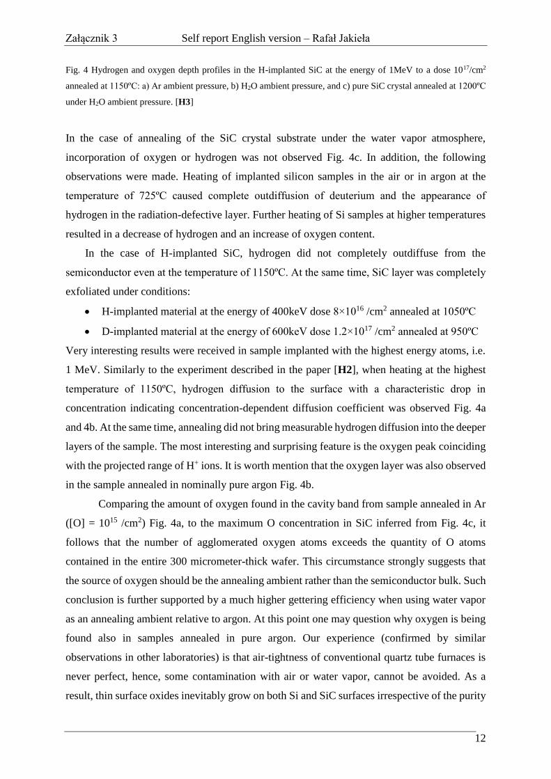
Fig. 4 Hydrogen and oxygen depth profiles in the H-implanted SiC at the energy of 1MeV to a dose 1017/cm2
annealed at 1150ºC: a) Ar ambient pressure, b) H2O ambient pressure, and c) pure SiC crystal annealed at 1200ºC
under H2O ambient pressure. [H3]
In the case of annealing of the SiC crystal substrate under the water vapor atmosphere,
incorporation of oxygen or hydrogen was not observed Fig. 4c. In addition, the following
observations were made. Heating of implanted silicon samples in the air or in argon at the
temperature of 725ºC caused complete outdiffusion of deuterium and the appearance of
hydrogen in the radiation-defective layer. Further heating of Si samples at higher temperatures
resulted in a decrease of hydrogen and an increase of oxygen content.
In the case of H-implanted SiC, hydrogen did not completely outdiffuse from the
semiconductor even at the temperature of 1150ºC. At the same time, SiC layer was completely
exfoliated under conditions:
H-implanted material at the energy of 400keV dose 8×10¹⁶ /cm2 annealed at 1050ºC
D-implanted material at the energy of 600keV dose 1.2×10¹⁷ /cm2 annealed at 950ºC
Very interesting results were received in sample implanted with the highest energy atoms, i.e.
1 MeV. Similarly to the experiment described in the paper [H2], when heating at the highest
temperature of 1150ºC, hydrogen diffusion to the surface with a characteristic drop in
concentration indicating concentration-dependent diffusion coefficient was observed Fig. 4a
and 4b. At the same time, annealing did not bring measurable hydrogen diffusion into the deeper
layers of the sample. The most interesting and surprising feature is the oxygen peak coinciding
with the projected range of H+ ions. It is worth mention that the oxygen layer was also observed
in the sample annealed in nominally pure argon Fig. 4b.
Comparing the amount of oxygen found in the cavity band from sample annealed in Ar
([O] = 1015 /cm2) Fig. 4a, to the maximum O concentration in SiC inferred from Fig. 4c, it
follows that the number of agglomerated oxygen atoms exceeds the quantity of O atoms
contained in the entire 300 micrometer-thick wafer. This circumstance strongly suggests that
the source of oxygen should be the annealing ambient rather than the semiconductor bulk. Such
conclusion is further supported by a much higher gettering efficiency when using water vapor
as an annealing ambient relative to argon. At this point one may question why oxygen is being
found also in samples annealed in pure argon. Our experience (confirmed by similar
observations in other laboratories) is that air-tightness of conventional quartz tube furnaces is
never perfect, hence, some contamination with air or water vapor, cannot be avoided. As a
result, thin surface oxides inevitably grow on both Si and SiC surfaces irrespective of the purity

Załącznik 3 Self report English version – Rafał Jakieła
13
of gases released to the furnace. However, because the low solubility, the supply of oxygen
from the surface oxide to the gettering layer cannot account for the magnitude of the observed
effect.
We postulated that the only path for oxygen agglomeration is migration of gaseous O2
or H2O from the edge of the sample through the porous layer. The exact nature of such lateral
diffusion remains to be further explored. There is no doubt, however, that the circumstance
favoring this before unseen process is the considerable porosity of the buried layer, with voids
and cavities visible in the TEM image.
5.4 Hydrogen properties in gallium nitride [H4]
The increase of interest in research on hydrogen in gallium nitride occurred when fabrication
of GaN based p-n junction was attempted. Unfortunately, the magnesium doped GaN layers
were highly resistive despite very high dopant concentration. The hydrogen passivation of
magnesium, which forms inactive complexes with a dopant was showed by Nakamura [17].
The annealing of the layers at suitable temperature results in the breaking of Mg-H bonds and
thus activation of magnesium. Interestingly, subsequent experiments on hydrogen in GaN at
low temperatures showed a complete lack of hydrogen atom mobility up to 900° C in GaN as
well as InN or AlN [18]. It would follow that when heating GaN crystals at high temperatures,
hydrogen bonds with magnesium are broken, but atoms are not removed from the material.
Subsequent studies have shown, that the acceptor conductivity in the GaN layers grown by
MBE can be extinguished by introducing hydrogen into the material. [19].
The variation of hydrogen mobility in materials with different Fermi levels been explained from
the first principles calculations [20]. Hydrogen as a proton H+ prefers the position close to the
nitrogen, forming a bond similar to that found in NH3 ammonia. Among the possible positions
of both atoms, the nitrogen antibonding site is the energetically most stable. Interestingly, this
is a different position than in Si or GaAs, due to the polarity of gallium nitride. The activation
energy for migration of bound hydrogen as 0.7 eV was calculated. For neutral hydrogen HO,
much smaller energy differences were found according to different sites. The energetically most
stable site for HO is the Ga antibonding site. For a proton with two electrons H–, the Ga
antibonding site is energetically most stable, as well as in the tetrahedral interstitial site, where
the distance between hydrogen and the neighboring Ga atoms is maximized, and the charge
density of the bulk crystal has a global minimum. In this position, the energy barrier for
hydrogen migration is as much as 3.4 eV. The charge state of hydrogen in GaN affects its

Załącznik 3 Self report English version – Rafał Jakieła
14
diffusion coefficient. In an n-type material (eg GaN: Si) this parameter is much lower than in a
p-type material (e.g. GaN: Mg), which was shown by calculations from the first principles
[21,22] and confirmed experimentally in the hydrogen implanted [23], plasma diffused [24, 25]
or epitaxial [26] GaN layers.
During my collaboration with the Epitaxy Lab at ITME, one of the first tasks was to develop a
method for removing hydrogen from GaN:Mg layers grown by the MOCVD method. Thus, the
heat treatment of a series of GaN samples at various temperatures and atmospheres was carried
out. The concentration of hydrogen in the heated layers was determined by the SIMS method.
The paper published in Optica Applicata [27] summarize the results of our studies. SIMS
measurements showed that annealing at 900°C for 15 min in N2 atmosphere allows removed
hydrogen to the background level of 1018 at/cm3.
Simultaneous SIMS depth profiling of hydrogen and magnesium allowed me to develop a
methodology for Mg measurement in GaN using negative ions, which is a non-standard method
for electropositive element. I have shown that the Mg profile can be obtained by measuring the
MgGaN⁻ ion cluster, obtaining Mg detection limit in GaN at the concentration level of 1017
at/cm3.
In the experiment with hydrogen diffusion in GaN layers with different types of conductivity
described in the article [H4] we showed the dependence of the diffusion coefficient on the type
of doping. However, unlike previous works, the experiment was conducted on homoepitaxial
GaN layers with low (107 /cm2) dislocation density. It allowed observing diffusion in the bulk
crystal and reducing the effect of hydrogen diffusion through dislocations.
For this purpose, 4 different layers with dislocation density and conductivity type shown in
Table 1 were annealed in the MOCVD reactor at a temperature of 1020ºC under the H2-NH3
atmosphere for 20 min.
Sample Dislocation density
(1/cm2)
Conductivity type and
carrier concentration
(1/cm3)
bulk crystal 107 n = 6.1×10¹⁸
GaN:Mg layer (MBE) 107 p = 3.5×10¹⁷
GaN:Si layer - template 5×10⁸ n = 3.6×10¹⁸
GaN:Mg layer (MOCVD) 5×10⁸ p = 7.2×10¹⁷
Table 1. Samples used in the experiment

Załącznik 3 Self report English version – Rafał Jakieła
15
The SIMS was the key method used to study the hydrogen depth profiles. The main difficulty
in SIMS measurement was achieving low hydrogen detection limit in GaN:Mg layers 0.5
micron and GaN:Si layers 1.5 micron thick. For such thin GaN layers, the primary beam current
and the setting of the secondary beam optics must be adequate to achieve proper detection (low
hydrogen background) at suitable depth resolution. In my measurement hydrogen detection at
the level of 2×10¹⁷ at/cm3 was achieved, which is the value only a one order of magnitude higher
compared to that achieved in the bulk GaN [H6], where the higher primary beam current
densities can be used.
We showed a high hydrogen diffusion coefficient in p-type (Fig. 5a and 5b), and no hydrogen
diffusion in n-type gallium nitride layers (Fig. 5c and 5d).
a) b) c) d)
Fig. 5 SIMS depth profiles in: a) as deposited GaN:Mg layer, b) annealed GaN:Mg layer, c) as deposited GaN:Si
layer, d) annealed GaN:Si layer. [H4]
Luminescence measurements carried out on the samples showed the greatest effects in the
GaN: Mg layer obtained by the MBE method. In the layer, which the SIMS measurement did
not show the presence of hydrogen before annealing and a high hydrogen concentration after
annealing (Fig. 5a and 5b), a decrease and shift of the "blue" luminescence and an increase in
the "yellow" luminescence compared to the original sample were observed. The effect most
likely resulted from the passivation of the Mg dopant by hydrogen through the formation of
Mg-H complexes (reduction of "blue luminescence"), and the formation of hydrogen complexes
with the VGa-H gallium vacancy ("yellow luminescence").
5.5 Oxygen properties in silicon [H5]
The above work was devoted to the subject probably best studied by our group, namely the
study of thermodynamic properties of oxygen in silicon using the SIMS method, based on its
solubility and diffusion. The first results of these studies were published in the paper [28] before

Załącznik 3 Self report English version – Rafał Jakieła
16
my Ph.D. degree. Publication [H5], which was submitted last year to the journal entitled Surface
and Interface Analysis, is a summary of our years-long research in this field, conducted mainly
on silicon detectors developed for the European Hadron Collider of the European
Organization for Nuclear Research CERN.
In silicon, similarly to SiC, stable planar SiO2 films serve as insulators, masks, and gate barriers
in metal‐oxide semiconductor transistors. Czochralski‐grown Si wafers usually contain oxygen
in quantities 7–10×1017 at/cm3. At room temperature, oxygen‐supersaturated Si is stable as the
oxygen atoms occupy predominantly bond‐centered interstitial sites in the lattice [29]. At
elevated temperatures, diffusion of oxygen leads to its aggregation into SiOx precipitates and to
the migration of atomic oxygen toward the external boundaries of the sample [30]. If the oxygen
content is sufficiently low, as in the float zone (FZ) silicon, it is possible to indiffuse oxygen
into the semiconductor from thermally grown or deposited SiO2 film [31].
To determine principal quantities characterizing the behavior of oxygen in Si, diffusivity (D)
and solid solubility (Cs) have been subject to numerous investigations employing a wide
spectrum of methods. However, SIMS delivers combined information on the depth profile of
both isolated and agglomerated species. Heating of supersaturated silicon leads to outdiffusion
of the interstitial O atoms and their segregation to the surface oxide, leaving a so‐called
“denuded zone” in the semiconductor.
The resultant surface concentration, Csurf(out), has commonly been taken as the solid solubility
of oxygen Cs at a given temperature [32, 33, 34]. However, we have shown that a correct
measure of Cs is the surface concentration Csurf(in) that is being set upon indiffusion of oxygen
into an FZ Si [28]. This is because atomic diffusion is an equilibrium process and, applying
sufficiently rapid quenching to room temperature, the precipitation can be effectively
suppressed. The outdiffusion profile cannot provide reliable information on the solid solubility
of oxygen because the atomic diffusion is accompanied by aggregation into immobile SiO2
precipitates that cannot be removed by diffusion. As a consequence, Csurf(out), determined from
SIMS data, always appears higher than Csurf(in). Regarding the diffusion coefficient of oxygen
in Si, determination of which requires only relative values of the concentration profile, our
findings do not deviate appreciably from the previously established data [35]. Our corrected
formula for Cs is:
)(2257,1
101,9 kT
eV
eCS

Załącznik 3 Self report English version – Rafał Jakieła
17
Our considerations on the measurement of oxygen in silicon by the SIMS method should be
started with the detection limit of this element. Fig. 6 summarizes the measured oxygen
concentration in different types of silicon that we have dealt with:
Fig. 6 Oxygen concentration levels measured in Si CZ, Si FZ, and in
epitaxial Si grown on either CZ or FZ silicon. [H5]
The values of 1018 at/cm3 and 1016 at/cm3 are considered typical for Si CZ and Si FZ,
respectively.
Our record low O signal of 2×10¹⁵ at/cm3 was obtained for silicon grown by atmospheric
pressure CVD, on Si FZ substrate. This value coincides with the detection limit of oxygen in Si
predicted by Gnaser [36] through extrapolation of the experimental data to the ideal vacuum in
the analysis chamber. The plot shown was taken after several minutes of uninterrupted sputter
etching with Cs beam at the energy of 14.5 keV. It should be noted that this result was achieved
by using a chromate cesium container in the ion source, yielding a beam of 600 nA current, ie,
twice higher than the current of a carbonate cesium source that we routinely use. A series of
tests with different raster sizes indicated that the detected O signal originates from the O‐
containing particles that adsorb on the analyzed surface and not from sample bulk. These
particles are likely to be resputtered by multiply scattered primary Cs ions. One such test is
shown in the Fig. 7.
Fig. 7. Raw data of SIMS depth profile of oxygen in Si. A step in Si profiles
is caused by increase of primary beam current density (raster change) [H5]
0 100 20010
1
102
103
104
105
106
107
108
109
1010
O
30
Si2 28
Si
SIM
S S
ignal (
c/s
)
Sputter time (s)
0 100 200 300
1015
1016
1017
1018
x10
Si:P epi / Si FZ
Si FZ
Si epi / Si CZ
Si CZ
Oxygen c
oncentr
ation (
at/cm
3 )
Sputter time ( s )

Załącznik 3 Self report English version – Rafał Jakieła
18
At first, the surface was raster‐scanned over 200 μm × 200 μm area, then the raster was reduced
to 50 μm × 50 μm while keeping the probing area unchanged. The O signal does not follow the
signals from silicon, which means that the source of “measured” oxygen is located outside the
sample bulk. In our system, the conversion factor from SIMS signal to oxygen concentration
relative sensitivity factor (RSF) amount 1019. Than oxygen concentration is calculated as
follows:
)/(10 319
230
16
cmatI
IC
Si
OO
where: CO – oxygen concentration, O
I 16 – oxygen signal, 2
30SiI – silicon signal.
Thus, the result presented in the Fig. 7 indicates that silicon epitaxial layers have an extremely
low concentration of oxygen (<1015 at/cm3), while oxygen adsorption during such a sensitive
measurement have to be monitored and minimized as much as possible. It is noteworthy that
there is no confirmation in the literature for such a low oxygen content in Si. Most epitaxial
structures are produced on a silicon substrate obtained by the Czochralski method with an
oxygen concentration above 1018 at/cm3, which diffuses into the layer when growing at 1100°C.
Achieving a low detection limit requires a high current density of the primary beam so that the
flux of oxygen secondary ions sputtered from the material prevails over adsorption rate of the
oxygen‐containing species. However, while the adsorption rate of residual gases may be
assumed constant, the resputtering caused by the (back) scattered incident Cs ions will scale
with the primary current. Also, the removal speed cannot be excessive when fine features in the
concentration profile have to be distinguished. Distribution of oxygen implanted into the epi‐Si
was measured with the sputtering rate of ~20 nm/s (Fig. 8). The oxygen implantation parameters
were energy 210 keV and a dose of 5×10¹⁴ /cm2. Here, the background level, below 1016 at/cm3,
could have been lowered by using higher current but at the expense of the profile definition.
Fig. 8. Depth profile of oxygen‐implanted epi‐Si. Dose 5×10¹⁴ at/cm2,
energy 210 keV [H5]
0 500 1000 1500 2000 250010
15
1016
1017
1018
1019
1020
O
30
Si2
Oxygen c
oncentr
ation (
at/cm
3 )
Depth ( nm )

Załącznik 3 Self report English version – Rafał Jakieła
19
Application of the conditions described above allowed studying the oxygen kinetics in Si
crystals. On Fig. 9 the oxygen profiles in Si as received under different annealing condition are
shown.
Fig. 9. Oxygen profiles: - outdiffusion form CZ Si (red), - diffusion into FZ
Si (blue), - diffusion into FZ Si at temp. 1150°C (black), - after additional
annealing the previous sample (green) [H5]
The most important result is the difference in surface concentrations of oxygen in FZ (low O
concentration) and Czochralski (high O concentration) silicon crystals after annealing at
1000°C. Oxygen diffuses into the Si FZ, while it outdiffuses from the Si CZ. The surface
concentrations of oxygen are not identical despite equal heating conditions. It is different when
oxygen is diffused at a higher temperature (black profile) and then annealed it in a lower
temperature (green) profile. Then the surface concentration of oxygen becomes comparable
under the same annealing conditions (green and blue profile).
A common observation is that heating of Si CZ crystal containing ~1018 at/cm3 results in
outdiffusion of oxygen to the oxide with surface concentration pinned at a value depending on
the solid solubility and degree of precipitation for a given temperature. Theoretically, however,
if Si with atomically clean, oxide‐free surface could be subjected to heat treatment in an inert
gas, a zero oxygen concentration at the surface should be observed.
One method to realize such artificial situation is to heat the Si wafer in vacuum. We have
employed a vacuum chamber used for evaporation of metals. Oxygen profiles in Si crystal
annealed under such condition are presented on Fig. 10.
0 10 20 30
1016
1017
1018
CZ 5h Ar
FZ 5h Ar
in-diffused FZ @ 1150 OC
in-diffused FZ + 5h Ar
10000C
Oxygen c
oncentr
ation (
at/cm
3 )
Depth ( m )

Załącznik 3 Self report English version – Rafał Jakieła
20
Fig. 10. Oxygen diffusion profiles into Si FZ (black) and outdiffusion
form Si CZ (red) as annealed at 1150°C, effect of 5 min. annealing in
vacuum at 1150°C for CZ Si (blue) and FZ Si (green) [H5]
Oxygen profiles for both bare CZ and previously indiffused FZ Si at 1150°C exhibit a deep
depletion near the surface, with surface concentrations ~10× lower than the corresponding
values for annealing in argon. This result shows, that the native oxide was removed by
sublimation and a clean Si surface was exposed to vacuum. In such case, oxygen freely
outdiffuses from the crystal.
For some applications, there is a need to monitor the oxygen distribution over large depths up
to the entire thickness of the wafer. Such is a case of indiffusion of oxygen from both sides into
an FZ Si for enhanced radiation hardness of charged particle detectors. In this situation, when
the depth of the eroded crater becomes comparable with its lateral size, substantial redeposition
of material on the crater bottom and resputtering from the crater walls make the resultant profile
unreliable, as shown in Fig. 11. To get correct values, beveling of the sample is necessary,
followed by step‐by‐step measurements. Enlarging the crater to dimensions typically used for
“nonatmospheric” species would improve the depth resolution but degrade the detectability
limit (not to mention the unacceptable increase of the time of analysis).
Fig. 11. Comparison of different results concerning deep O diffusion into
FZ Si: (1) calculated numerically with D=2×10⁻¹⁰ cm2/s, CO=1.7×10¹⁷
at/cm3, (2) line scan on a beveled surface with a background correction (3)
dynamic SIMS profile.
0 5 10 15 20 2510
16
1017
1018
1150oC
CZ 1h Ar
CZ 5 min vacuum
FZ 1h Ar
FZ 1h Ar + 5 min vacuum
Oxygen c
oncentr
ation (
at/cm
3 )
Depth ( m )
0 50 100 150 200 25010
15
1016
1017
1018
as calculated
line scan
continuous profiling
1150°C, 24 h
Oxygen c
oncentr
ation (
at/cm
3)
Depth ( m )

Załącznik 3 Self report English version – Rafał Jakieła
21
5.6 Properties the atmospheric elements in wide-bandgap semiconductors (H6)
The above publication is a review and summary of years-long research related to the detection
and profiling of atmospheric elements in wide-band semiconductors such as GaN, ZnO and SiC
performed in our laboratory. The publication contains four sections on the properties of
particular atmospheric elements, i.e. H, C, N and O. The first chapter concerns the properties
of hydrogen in GaN, ZnO and SiC, the second chapter describes the properties of carbon in
GaN and ZnO, the third chapter concerns the properties of nitrogen in ZnO and SiC, while the
fourth chapter describes the properties of oxygen in GaN and SiC. All chapters also contain the
methodology of SIMS measurements for mentioned elements in the relevant materials,
developed based on my own measurement experience. For this purpose, standards of studied
elements in the defined semiconductors were prepared as the implanted samples with a specific
dose D and implantation energy E:
a) Hydrogen in:
GaN – D=1e16 cm-2, E=25 keV,
ZnO – D=1e16 cm-2, E=250 keV,
SiC – D=1e16 cm-2, E=150 keV
b) Carbin in:
GaN – D=1e16 cm-2, E=350 keV,
ZnO – D=1e16 cm-2, E=500 keV,
c) Nitorgen in:
ZnO – D=8.6e15 cm-2, E=500 keV,
SiC – D=2e16 cm-2, E=100 keV,
d) Oxygen in:
GaN – D=1e16 cm-2, E=400 keV,
SiC – D=5e15 cm-2, E=100 keV.
All standards were measured by the SIMS method under the following measurement conditions:
a) O2+ beam at 8keV, positive secondary ions, primary beam current 800 nA, sputtered
area R=200×200 m,
b) Cs+ beam at 5.5keV, positive secondary ions, primary beam current 200 nA, sputtered
area R=200×200 m,
c) Cs+ beam at 14.5keV, negative secondary ions, primary beam current 200 nA, sputtered
area R=200×200 m,

Załącznik 3 Self report English version – Rafał Jakieła
22
equal for all elements. Comparison of depth profiles of atmospheric elements for individual
measurement conditions has allowed to determine the best SIMS measurement methodology.
Although all atmospheric elements provide the best detectability as negative ions, a
methodology for measuring these elements as positive ions was developed. The results
described in the paper [H6] present the circumstances and possibilities of atmospheric elements
detection as positive secondary ions. This is particularly applicable when the simultaneous
study of atmospheric elements with electropositive elements is crucial for understanding the
processes occurring in semiconductor material. Examples of such measurements published in
peer-reviewed journals are collected in references to this work.
Particular importance was placed on the detection of nitrogen, which of all atmospheric
elements has the lowest electron affinity and the highest ionization energy. These parameters
are extremely unfavorable for the SIMS measurement, compared to the other elements from the
Periodic Table. In the publication [H6] I described the methodology needed to achieve adequate
nitrogen detection (detection of the lowest concentrations) by measuring its clusters with other
elements, i.e. N-Si and N-C in silicon carbide or N-O in zinc oxide.
The work also contains the result of SIMS measurement showing the lowest detection limit of
atmospheric elements in gallium nitride obtained by the Halide Vapor Phase Epitaxy method
Appropriate methodology allowed to achieve the hydrogen detection at the level of 8×10¹⁵
at/cm3, carbon – 5×10¹⁵ at/cm3 and oxygen – 1016 at/cm3 (Fig. 12)
Fig. 12. Depth profiles of H, C, O and Si in GaN bulk crystals [H6]
Characteristic drops on the SIMS profiles of particular ambient elements result from testing the
analytical methodology by increasing the density of the primary beam current with appropriate
settings of the secondary beam optics.

Załącznik 3 Self report English version – Rafał Jakieła
23
The implanted samples were also used as standards for determining the relative sensitivity
factors (RSF) for studied elements, enabling the quantitative determination of atomic
concentration.
The bibliography of the publication [H6] contains nearly 50 references in which my SIMS
measurements were an important contribution to understanding the results presented in the cited
papers.
6. Bibliometric information
6.1 Total Number of Publications
191 including 160 after obtaining a Ph.D. degree in Physics. The papers were published in
peer-reviewed journals having high international reputation, such as:
Acta Physica Polonica – 21 articles (all after obtaining Ph.D. degree)
Journal of Crystal Growth – 14 articles (including 13 after obtaining Ph.D. degree)
Applied Physics Letters – 13 articles (including 10 after obtaining Ph.D. degree)
Journal of Alloys and Compounds – 12 articles (including 11 after obtaining Ph.D.
degree)
Physical Review B – 9 articles (all after obtaining Ph.D. degree)
Semiconductor Science and Technology – 8 articles (including 7 after obtaining Ph.D.
degree)
Journal of Physics: Condensed Matter – 4 articles (all after obtaining Ph.D. degree)
Journal of Applied Physics – 4 articles (all after obtaining Ph.D. degree)
6.2 Total Impact Factor of publications
after the Journal Citation Reports (JCR) according to year of publication = 302
6.3 Total citation number of publication
after the WoS base on 20/01/2020 = 1974 including without autocitation 1737
6.4 Hirsch Index of publication
after the WoS base on 20/01/2020 = 22

Załącznik 3 Self report English version – Rafał Jakieła
24
7. Presentation of significant scientific activity carried out at more than one university,
scientific or cultural institution, especially at foreign institutions.
7.1 Scientific work before obtaining a Ph. D. degree in physics
After graduating from the Electronic Technical School in Rzeszów in 1994, I started studying
at the College of Sciences in Warsaw, the Non-Public Higher School at the Polish Academy of
Sciences. After passing three years of study and doing two bachelor classes entitled: a)
Microwave rotational and oscillatory particle spectroscopy under the advisory of prof. Z.
Kisiel, and b) Low-temperature transport properties of PbTe layers grown by MBE method
under the advisory of prof. G. Grabecki, I obtained a bachelor's interdisciplinary degree in
physics, chemistry and mathematics. Then I continued my master's studies in the topic of
physical measuring devices. Simultaneously, I started a student internship in a newly created
SIMS laboratory equipped in the new CAMECA IMS6F spectrometer under the advisory of
prof. Adam Barcz. In addition to the improvement of SIMS measurements, I conducted
research on the diffusion and activation of silicon dopant in GaAs. Master's studies were
completed with presenting of the master's thesis entitled Silicon implantation into GaAs, under
the advisory of prof. Adam Barcz.
After receiving a master's degree, I have begun Ph. D. studies at the Institute of Physics of the
Polish Academy of Sciences in the SIMS laboratory under the supervision of prof. Adam
Barcz. Simultaneously I started cooperation with the group of Semiconductor Epitaxial Growth
at Institute of Electronic Material Technology (IEMT). The aim of the cooperation was
studying the GaAs-, InP- and GaN-based semiconductor structures grown by the MOCVD
method. Cooperation has led to significant progress in the characterization of semiconductor
structures using the SIMS method, which allowed to produce an increasingly better quality
structures. It resulted in many publications regarding the properties and parameters of epitaxial
growth of materials such as InP [37,38], GaN [39,40], InGaAs [41,42,43].
Cooperation with the laboratory of semiconductor epitaxy, allowed also to conduct my own
research on the dopants diffusion in gallium nitride. The result of this research concerning the
removing of hydrogen from the GaN:Mg layer resulting in activation of magnesium dopant,
was published in the journal Optica Applicata [44].
In order to improve the SIMS measurement technique, I completed a two-week internship at
the SIMS laboratory at the Chalmers University of Technology in Gothenburg. During my
stay, I resolved the calibration procedure allowing to determine the composition of the ternary
semiconductor compound (Ga,Mn)As.

Załącznik 3 Self report English version – Rafał Jakieła
25
As part of my Ph.D. studies I conducted research on the dopants diffusion in semiconductor
materials. One of the topic of research concerned the oxygen diffusion in silicon crystals. The
results were published in the journal Vacuum [45] and Semiconductor Science and Technology
[46]. However, my main interests concerned the dopants diffusion in III-V materials. The first
research topic was the diffusion and activation of silicon in gallium arsenide. As part of these
studies, the effect of doping, and thus the Fermi energy level, on Si diffusion in GaAs was
observed. The results have been published in the journal Vacuum [47]. At the same time, I
conducted the research resulting from the work on InP-based photodetectors carried out at
ITME, concerned the Zn diffusion in InP. In this material, the influence of the annealing
conditions on the generation of indium and phosphorus vacancies as well as the concentration-
dependent diffusion coefficient were observed. The results were also published in the Vacuum
journal [48]. Another research subject resulting from previous studies was the Si diffusion in
gallium nitride. The main conclusion was the influence of the annealing conditions on the
generation of Ga vacancies participated in silicon diffusion. The studies were presented at the
ICNS-6 conference in Bremen and published in the journal physica status solidi (c) [49]. The
last research topic resulting from the increased interest in dilute magnetic semiconductors was
the diffusion of manganese in the gallium arsenide. As in previous studies, the influence of the
annealing conditions on the diffusion coefficient was examined, and the concentration-
dependent diffusion coefficient was also observed. The results have been published in the
journal Journal of Alloys and Compounds [50]. Interesting research on Mn diffusion in CdTe
was conducted in cooperation with prof. Karczewski group and have been published in the
journal Thin Solid Films [51].
As part of the cooperation between the SIMS laboratory and the laboratories of the Institute of
Physics Polish Academy of Sciences, I conducted research on dopants and impurities in bulk
crystals of ZnO [52,53] (ON 1.1 department under the leadership of prof. A Mycielski) and
ZnO layers grown by ALD method [54] (ON 4.2 department under the leadership of prof. M.
Godlewski). In addition, I have established cooperation with leading polish institutes dealing
with semiconductor technologies. For the Department of Micro- and Nanotechnology of Wide
Bandgap Semiconductors at Institute of Electron Technology (IET), under the leadership of
prof. Anna Piotrowska I performed SIMS characterization supporting the research on ZnO
layers [55, 56, 57, 58, 59] and contacts for the wide-bandgap semiconductors [60, 61, 62, 63].
For High Pressure Research Center (HPRC), Polish Academy of Sciences I characterized
Mg-doped GaN layers grown by MBE method [64].

Załącznik 3 Self report English version – Rafał Jakieła
26
Also, I conducted research in cooperation with many foreign laboratories. For MBE laboratory
at Physikalisches Institut Universitat Wurzburg, I characterized (Ga,Mn)As layers [65, 66].
Cooperation with Lawrence Berkeley National Laboratory in the study of hydrogen and
oxygen impurities in one of the first InN layers obtained by the MBE method resulted in the
publication with the largest number of citations in my bibliography (195) [67]. Improvement of
SIMS and capacitance-voltage profilometer measurements for studying the diffusion and
electrical properties of dopants in GaAs, InP and GaN semiconductors was the main topic of
my Ph.D dissertation entitled: Diffusion mechanisms in A3B5 semiconductors under the
advisory of prof. A. Barcz (June 2005) As part of my Ph. D. studies, I also wrote a software
for converting raw data obtained from the SIMS apparatus to a format that facilitates their
import into the Origin program. I have also written software that simulates diffusion in various
thermodynamic conditions and parameters of atomic mobility. The studies for the Ph.D. thesis
resulted in two more publications on diffusion of Mn in GaAs and Si in GaN.
7.2 Scientific work after obtaining a Ph. D. degree in physics
After obtaining the Ph. D. degree I continued cooperation with the laboratories of the Institute
of Physics PAS as well as with other institutes dealing with semiconductor technologies, i.e.
IEMT, IET and HPRC PAS.
I also expanded my cooperation with polish and foreign institutes. A great contribution to the
research on doping and impurities of GaN bulk crystals brought the cooperation with Ammono
company started in 2007. However, for commercial reasons, no publications were allowed.
Similar cooperation was established with the VIGO company, for characterization the CdTe-
based semiconductor structures.
I continued research on the diffusion and activation of atoms in semiconductors. Due to the
increasing attractiveness of dilute magnetic semiconductors (DMS) one of the first steps of my
research after Ph.D. was the characterization of Fe diffusion in gallium nitride. The results were
presented as a poster on Jaszowiec 2006 and ELTE 2007 conferences.
Another subject of my study closely related to the habilitation thesis was the diffusion of oxygen
in gallium nitride. As part of this research, I wrote a proposal for the project SPIRIT (Support
of Public and Industrial Research using Ion Beam Technology) and I received the contract
for research entitled Oxygen diffusion into GaN from oxygen or argon implanted Al2O3. Within
this project, I passed a one-week internship at Helmholtz-Zentrum Dresden-Rossendorf Ev
to perform oxygen implantation into GaN and Al2O3 crystals. The results of research on oxygen
diffusion in GaN were published in the journal Physica Status Solidi C [68] and presented as a

Załącznik 3 Self report English version – Rafał Jakieła
27
poster presentation on Jaszowiec 2009 and The 3rd International Symposium on Growth of III-
Nitrides in Montpellier conferences.
Another research topic carried out under the statute of the Institute of Physics Polish Academy
of Sciences and related to the habilitation thesis, was the diffusion of hydrogen in silicon carbide
crystals. Differently doped and H-implanted SiC crystals were annealed by the rapid thermal
annealing method (RTA). The dependence of the diffusion coefficient on the doping type and
oxygen segregation effect was shown. The results were published in Journal of Apllied Physics
[69] and Nuclear Instruments and Methods in Physics Research B [70]. The studies on As
diffusion in zinc oxide crystals annealed under controlled pressure of arsenic vapors resulted in
the publication on As properties in ZnO published in Journal of Alloy and Compounds [71],
and poster presentation on Jaszowiec 2013 conference.
Cooperation with a prof. Maciej Sawicki group concerning dilute magnetic semiconductors
such as (Ga,Mn)N layers grown by MBE method resulted in interesting results regarding the
influence of residual oxygen on Mn diffusion in GaN. These findings have been published in a
renowned Journal of Alloy and Compounds [72] and presented at 34th International Conference
on Physics of Semiconductors 2018 in Monpellier and 7th International Symposium on Nitride
Growth 2018 in Warsaw.
Simultaneously with the research on the atomic diffusion in semiconductors, I have improved
the technique of SIMS measurements and presented the results at conferences on mass
spectrometry [73, 74, 75].
Even before the Ph.D. title, I have established cooperation with the European Organization
for Nuclear Research CERN oriented to silicon-based detector structures. Silicon detectors
manufactured at CERN and our own samples were prepared to study thermodynamic properties
and oxygen diffusion mechanisms in the silicon crystal. This extensive study resulted in a
comprehensive work published in the journal Surface and Interface Analysis [76]. In this paper
we report on the detection of very low oxygen concentration in silicon by SIMS method.
Applying a very high primary Cs+ ion flux, prolonged presputtering, extensive vacuum
chamber baking, titanium sublimation pump, and an liquid nitrogen (LN) trap, we have reached
a detection limit of ~2×10¹⁵ at/cm3 in chemical vapor deposition epitaxial Si films. This value
appears to be at least 10 times lower than in any published or unpublished source known to the
authors, including the reference sensitivities listed by the instrument manufacturer. Most likely,
the key improvement that has allowed us to drive the detection limit to 1015 at/cm3 is the use of
an ion pump in the analysis chamber. This paper demonstrates optimized analytical conditions
for the oxygen measurements in Si, as a function of depth:

Załącznik 3 Self report English version – Rafał Jakieła
28
very shallow profiles are practically impossible to measure accurately because of
native oxide at the surface,
shallow – to – medium range profiles, up to ~20 μm, are the most amenable to SIMS
measurements,
medium – to – deep (~20‐50 μm) range is required to follow interdiffusion and
segregation in epitaxial layers when the oxygen – free layer is grown on a CZ Si
substrate,
extremely deep profiles, up to full thickness of the wafer, definitely necessitate
beveling.
Our studies elucidated oxygen indiffusion and outdiffusion during annealing in Ar and in
vacuum, noting that the results are qualitatively and quantitatively different for FZ Si as
compared with CZ Si. We pointed out that using FZ Si and the indiffusion method provides the
most accurate values of the equilibrium oxygen solubility concentration.
For the research in cooperation with laboratories at the Institute of Physics PAS the most
abundant with respect to the SIMS characterization were studies of the layers grown by the
ALD method in the ON4.2 division led by prof. Marek Godlewski. Together with scientists
from this laboratory, we have published 31 papers. The majority of them concerned zinc oxide
and its properties [77, 78, 79, 80, 81]. Published papers were in particular related to the defects
[82, 83], dopants [84, 85, 86, 87, 88] and electronic properties [89, 90] of ZnO. The SIMS
characterization of zinc oxide layers consisted mainly of the study of impurities, i.e. H or C,
and dopants, i.e. N or Al. ZnO-based dilute magnetic semiconductors (DMS) performed by
adding Co or Mn elements to the matrix were also widely studied [91]. The research on a such
materials concerned the growth [92, 93, 94], optical [95, 96, 97], or electrical and magnetic [98,
99, 100, 101, 102] properties. Characterization by the SIMS method was to examine the amount
of embedded magnetic elements, homogeneity of doping and the impurities incorporation. For
this purpose, appropriate Co and Mn standards in ZnO were created, as well as the relative
sensitivity factor (RSF) coefficients were determined, allowing to calculate the content of both
elements with accuracy ±10%.
As part of cooperation with the ALD growth group, the research on the ZnMgO ternary
semiconductor [103], HfO2 as a diffusion barrier of ZnO/Ag junction [104] or Ti1−xNbxO2
properties grown by ALD method [105] was also started.
Equally publication-efficient is my cooperation with the Laboratory of Cryogenic and
Spintronic Research (SL2) of prof. Tomasz Dietl, and currently under the leadership of prof.

Załącznik 3 Self report English version – Rafał Jakieła
29
Maciej Sawicki in cooperation with Institut für Halbleiter- und Festkörperphysik
Johannes Kepler University (JKU) z Linz under the leadership of prof. Alberta Bonanni.
Together with colleagues from SL2, I became a co-author of 13 publications, most of which
were published in the renowned Physical Review B journal. As part of these studies, structural,
electrical magnetic [106, 107] and optical [108] properties of GaN:Fe, (Ga,Fe)N layers grown
by MOCVD, as well as the effect of Mg doping on epitaxial growth [109] were characterized.
Similar studies were conducted for GaN:Mn and (Ga,Mn)N layers [110, 111, 112]. In
cooperation of Institute of Physics PAS, JKU and Institute of Solid State Physics University
of Bremen groups, magnetic layers (Ga,Mn)N grown by MBE were also studied [113, 114].
One of the papers [115] was awarded of the director's award for the best paper of Institute of
Physics PAS of 2016 year. The scope of the research also included the Mg-doped GaN layers
[116, 117]. A part of the research employing SIMS measurements consisted in determining the
content of both the magnetic elements Fe and Mn, as well as the dopants, i.e. Mg and Si, but
also the H and O impurities.
Similarly, as for the ZnO, appropriate Mn and Fe in GaN standards were developed, allowing
determination of the atomic content of these elements in GaN layers up 10 at%. SIMS-
characterized manganese-doped layers brought insights into the measurement artifacts
associated with the Mn depth profiles, presented at the conference SIMS Europe 2016 [118].
Another scientific group from the Institute of Physics PAS, I had a close cooperation for a long
time, is the ON1.1 group under the leadership of prof. Andrzej Mycielski. The group mainly
deal with the growth of CdTe based bulk crystals. In addition to testing the purity of the
elements used to the crystal growth, my part of the study also included checking the
homogeneity and the stoichiometry, as well as doping level of the crystals. The scope of
publications with colleagues from the ON1.1 group refers to such subject as: fabrication of
contacts for semi-insulating crystals CdMnTe:V [119, 120, 121], CdMnTe and CdMgTe based
X-ray detectors [122, 123], growth and annealing of CdMnTe bulk crystals [124, 125] and
properties of Se doped CdTe bulk crystals [126]. The ZnO bulk crystals were also characterized
[127, 128].
As part of the statutory research of the Institute of Physics PAS, I also collaborated with ON1.2
group on molecular beam epitaxy growth the CdTe-based layers and crystals under the
leadership of prof. Tomasz Story and ON4.7 group dealing with molecular beam epitaxy of
ZnO of prof. Adrian Kozanecki. The scope of research in cooperation with the ON1.2 group
mainly involved the GeMnTe/BaF2 layer characterization [129, 130, 131, 132]. In the ON1.2
Załącznik 3 Self report English version – Rafał Jakieła
30
group I worked together with dr. hab. Ewa Przeździecka regarding the characterization of As
and Sb [133, 134, 135, 136, 137] or N [138, 139] doped ZnO layers grown by MBE method.
The continuation of research on the Mn diffusion in GaAs, started as part of my Ph. D. thesis,
was conducted with a SL1.2 research group of which I am a member, headed by prof. Krystyna
Ławniczak-Jabłońska. Within the EAGLE project, we investigated the local properties of Mn
atoms in GaAs crystals [140, 141, 142].
Other studies I took part in were: behavior of GaMnSb/GaSb annealed at the elevated
temperatures [143], properties of In/PbTe junction [144], properties of GaN/Si grown by MBE
method [145], structure of GaN/AlGaN superlattice [146], Co diffusion in Gd3Ga5O12 crystals
[147] and properties of (Ga,Mn)As and (Ga,Mn)(Bi,As) layers [148, 149].
After my Ph. D. thesis, I also continued cooperation with other Polish institutes dealing with
growth and crystal characterization. The largest number of projects, and thus publications,
resulted from joint projects with Department of Micro- and Nanotechnology of Wide Bandgap
Semiconductors led by prof. Anna Piotrowska and Department of Photonics under the
leadership of prof. Maciej Bugajski, both from Institute of Electron Technology (IET).
Research in cooperation with prof. Piotrowska group mainly relied on the characterization of
ZnO layers deposited by magnetron sputtering [150, 151]. Published research results
concerned: characterization of ZnO and ZnMnO layers produced by oxidation of Zn(Mn)Te
[152, 153, 154], ZnO doping by N, As or Sb elements [155, 156, 157] or ZnO doping by group
1B elements [158]. Other works devoted to the electric contacts for wide band-gap
semiconductor eg. Ti-Al-N [159, 160, 161] or Ni-Si [162]. The research conducted together
with the Department of Photonics concerned mainly the characterization of layers and devices
based on III-V semiconductors grown by the MBE method [163, 164, 165, 166, 167, 168, 169,
170]. For research groups from IET, I also characterized materials such as Si:Mn [171],
GaMnAs [172] and TaO2 [173].
After receiving the Ph.D. degree, I also continued cooperation with the Institute of Electronic
Materials Technology (IEMT) for the characterization of semiconductor layers based on
GaAs, InP, GaN and SiC grown by the MOVPE method [174]. The most fruitful cooperation
was brought with dr. Katarzyną Racką-Dzietko concerning the characterization of bulk SiC
crystals obtained by Physical Vapor Transport (PVT) method [175, 176, 177, 178, 179, 180,
181].
As for the cooperation with the High Pressure Research Center PAS I took part in
characterization of GaN materials manufactured by either MOVPE method ( prof. Tadeusz
Suski) [182, 183, 184, 185, 186] or using a novel Hydride Vapor Phase Epitaxy (HVPE) [187,

Załącznik 3 Self report English version – Rafał Jakieła
31
188, 189]. Properties of GaN crystals grown by Sublimation Sandwich Method (SSM) were
also studied [190, 191].
For completeness the list below comprises other studies of materials together with cooperating
institutions and publications:
(Ga,Mn)N layers [192, 193, 194] – Institute of Solid State Physics University of
Bremen,
(Ga,Mn)As [195, 196] and (In,Fe)As [197] layers – Helmholtz-Zentrum Dresden-
Rossendorf, Institute of Ion Beam Physics and Materials Research,
InSe:Mn [198, 199] and ZnO [200] – I. M. Frantsevich Institute for Problems of
Materials Science National Academy of Sciences of Ukraine,
HgCdTe:As [201, 202, 203, 204] – National Research Tomsk State University,
hydrogen diffusion in LiNbO3 [205] and Mn in YAlO3 [206] – Lviv Polytechnic
National University
(Ga,Mn)As [207, 208, 209] – Department of Physics University of Notre Dame,
SnTe:In [210] and InAlAs/InAs:Mn structures [211] – Institut fur Experimentelle
und Angewandte Physik Universitat Regensburg
GaN:Si/Al2O3 [212] – V. Lashkaryov Institute of Semiconductor Physics,
National Academy of Sciences of Ukraine.
Currently I am conducting a statutory research on Na diffusion and activation in zinc oxide
crystals. First results from the innovative method of introducing sodium into ZnO crystals from
aqueous NaCl solution at temperatures up to 300°C were presented at the 10th International
Workshop on Zinc Oxide and Other Oxide Semiconductors conference in Warsaw [213]. While
within the TECHMAGSTRATEG grant received by the Institute of High Pressure Physics PAS,
I characterize Be diffusion mechanisms in GaN crystals.
8. Presentation of teaching and organizational achievements as well as achievements in
popularization of science or art.
8.1 Creative professional works:
Coauthor of the book: Crystal Growth: Theory, Mechanism and Morphology, Chapter
9: MBE Growth of Type-II InAs/GaSb Superlattices on GaSb Buffer – A. Jasik, I.
Sankowska, K. Regiński, E. MAchowska-Podsiadło, A. Wawro, M. Wzorek, R.
Kruszka, R. Jakieła, J. Kubacka-Traczyk, M. Motyka, J. Kaniewski

Załącznik 3 Self report English version – Rafał Jakieła
32
Internship in the SIMS laboratory in Chalmers Institute in Goteborg, Sweden –
determination of the composition of AlGaN and MnGaAs layers by the SIMS method
Stay in Helmholtz-Zentrum Dresden – Rossendorf e.V., Germany according to project
of European Community as an Integrating Activity Support of Public and Industrial
Research Using Ion Beam Technology (SPIRIT) in order to carry out the research
entitled Oxygen diffusion into GaN from oxygen or argon implanted Al2O3
6 seminars, including 5 after obtaining Ph.D. degree
155 conference presentation:
- 2 coauthors of invited talk,
- 15 oral presentations (2 presented personally), including 11 after obtaining Ph.D.
degree (1 presented personally)
- 138 poster presentations (23 presented personally), including 109 after obtaining
Ph.D. degree (15 presented personally)
8.2 Managing and Participation in Domestic or International Research Projects before
obtaining Ph.D. degree
2001 – 2002, principal investigator in the government project KBN 7 11TB 001 21
entitled Si and Zn diffusion in InP performed in the Institute of Electronic Material
Technology
8.3 Managing and Participation in Domestic or International Research Projects after
obtaining Ph.D. degree
1996 – 1999, investigator in the government project KBN 8T11B08210 managed by
prof. A. Barcz, entitled: Study of thermodynamic properties of GaAs
2000 – 2003, investigator in the European Commission project IN LINE SIMS IST-
01-6-2B
2001 – 2005, investigator in the government project KBN 7T08A06021 managed by
prof. A. Barcz, entitled: Oxygen transport kinetics in the SiO2/Si FZ system
2008 – 2011 investigator in the government project MNiSW N507436834 managed
by prof. A. Barcz, entitled: Characterization of materials and SIC based structures -
SIMS, DLTS, I(C)-V
2009 – 2013, investigator in the project of ERC Advanced Grant Research – UE-27/1
managed by prof. T. Dietl, entitled: Functionalisation of Diluted Magnetic
Semiconductors FunDMS

Załącznik 3 Self report English version – Rafał Jakieła
33
2010, principal investigator of contract 227012 in the project SPIRIT (Support of
Public and Industrial Research using Ion Beam Technology) entitled: Oxygen
diffusion into GaN from oxygen or argon implanted Al2O3
2012 – 2017, investigator in the government project P-376/M managed by prof. T.
Dietl, entitled: Quantum phase transitions in magnetic layers controlled by an
external electric field
2014 – 2017, investigator in the government NCN project P-418/O managed by prof.
T. Dietl, entitled: Tunneling electrons and Cooper's pairs in quantum structures
containing a ferromagnetic insulator (Ga,Mn)N
2016 – 2018, investigator in the government project managed by prof. Andrzej
Mycielski, entitled: Insulating crystals (Cd,Mn)Te: Exploration and description of
spatial carrier transport and compensation conditions
2018 – now, investigator in the government project TECHMATSTRATEG
1/346720/8/NCBR/2017 managed by prof. Andrzej Mycielski, entitled: Technology
for the production of materials and structures for the detection of X and gamma
radiation, using low defect homogeneous crystals (Cd,Mn)Te, with high resistance to
defect generation as a result of irradiation
2019 – 2022, investigator in the government project NCN Opus 15 nr
2018/29/B/ST5/00338 managed by prof. Michał Boćkowski, entitled: Acceptors
implantation into intentional undoped GaN layers grown by the HVPE method -
structures that are the basis of vertical high power transistors
8.4 List of invited papers delivered at national or international conferences:
E. Kamińska, E. Przeździecka, A. Piotrowska, J. Kossut, E. Dynowska, A. Barcz, R.
Jakieła, W. Dobrowolski, I. Pasternak, P. Bogusławski – p-type doping in ZnO -
invited lecture – XXXV International School on the Physics of Semiconducting
Compounds, Jaszowiec 2006
Andrzej Mycielski, M. Witkowska-Baran, D. Kochanowska, A. Szadkowski, B.
Witkowska, W. Kaliszek, R. Jakiela, V. Domukhovski – (Cd,Mn)Te as a New
Material for X-ray and Gamma-ray Detectors – MRS 2007 Fall Meeting, Boston
8.5 Other papers personally delivered at national or international conferences:
R. Jakieła, A. Jasik, W. Strupiński, K. Góra, K. Kosiel, M. Wesołowski – Zależność
koncentracji wodoru w warstwach epitaksjalnych GaN:Mg od sposobu ich

Załącznik 3 Self report English version – Rafał Jakieła
34
wygrzewania – charakteryzacja metodą SIMS – IX Seminarium: Powierzchnia and
Struktury Cienkowarstwowe, Szklarska Poręba 2002
R. Jakiela, A. Barcz, J. Sarnecki, G. K. Celler – Ultra-high Sensitivity SIMS Analysis
of Oxygen in Silicon – 21st International Conference on SIMS, Kraków 2017
8.6 Seminars presented:
Charakteryzacja struktur półprzewodnikowych metodą SIMS – Seminarium Fizyki
Ciała Stałego Wydziału Przyrodniczego WSP Rzeszów, 2000
SIMS ? .. seems good ! – seminar in Ammono company, 2008
Spektrometria Masowa Jonów Wtórnych – Seminarium Rentgenowskie IFPAN –
2008
Transport atomowy w ciele stałym (2 seminars) – Konwersatorium ITME – 2008
Dyfuzja powierzchniowa – Konwersatorium ITME – 2008
Spektrometria Masowa Jonów Wtórnych – podstawy and zastosowanie w badaniach
struktur półprzewodnikowych – Seminarium Centrum Dydaktyczno-Naukowe
Mikroelektroniki and Nanotechnologii Uniwersytetu Rzeszowskiego – 2014
8.7 Construction of a unique science equipment
Service and maintenance of the secondary ion mass spectrometer – CAMECA IMS 6F
Adaptation of Capacitance-Voltage profilometer BIORAD PN4300 for the wide band
gap semiconductors
8.8 Organization of conferences, reviewing and editorial activities
Reviewer of article entitled P-type single-crystalline ZnO films obtained by (P,O) dual
implantation through dynamic annealing process for journal Superlattices and
Mictrostructures 2018
Reviewer of article entitled The effect of alpha particle irradiation on electrical
properties and defects of ZnO thin films prepared by sol-gel spin coating for journal
Material Science in Semiconductor Processing 2018
Reviewer of article entitled Structural and Optical Characteristics Investigations in
Oxygen Ion Implanted GaN Epitaxial layers for journal Material Science in
Semiconductor Procesing 2019

Załącznik 3 Self report English version – Rafał Jakieła
35
8.9 Didactics and popularization of science
Presentation of the SIMS laboratory on an annual Festiwal Nauki
Presentation of the SIMS laboratory on an annual Dni Otwarte Instytutu Fizyki PAN
Physics teacher in first class of high school with a biological - chemical profile
Notes in the science section of blog page Salon24.pl:
- Mercury - a rare possibility of observation.
- Semiconductor blue laser structure for lay people
- Two-dimensional electron gas in a field effect transistor
8.10 Patents and patent applications
patent co-author: PL218567, obtained on 20.05.2014 – A method for producing
semiconductor wafers from CdTe – Rafał Jakieła, Zbigniew Gołacki
patent co-author: PL215095, obtained on 15.04.2013 – The method of producing
heterostructures n-(Eu,Gd)Te/p-PbTe and heterostructure to generate random
numbers – Mąkosa Andrzej, Wrotek Sylwia, Dziawa Piotr, Osinnij Victor, Taliashvili
Badri, Tkaczyk Zbigniew, Jakieła Rafał, Figielski Tadeusz, Wosiński Tadeusz, Story
Tomasz

Załącznik 3 Self report English version – Rafał Jakieła
36
9. Bibliography
[1] W. Seifert, R. Franzheld, E. Butter, H. Sobotta, V. Riede – On the Origin of Free Carriers
in High-Conducting n-GaN – Crystal Res. & Technol. 18 (1983) 383
[2] B-C. Chung, and M. Gershenzon – The influence of oxygen on the electrical and optical
properties of GaN crystals grown by metalorganic vapor phase epitaxy – Journal of Applied
Physics 72 (1992) 651
[3] J. C. Zolper, R. G. Wilson, S. J. Pearton, R. A. Stall – Ca and O ion implantation doping of
GaN – Appl. Phys. Lett. 68 (1996) 1945
[4] S. J. Pearton, H. Cho, J. R. LaRoche, F. Ren, R. G. Wilson J. W. Lee – Oxygen diffusion
into SiO2–capped GaN during annealing – Appl. Phys. Lett. 75 (1999) 2939
[5] E. Dumiszewska, W. Strupinski, P. Caban, M. Wesolowski, D. Lenkiewicz, R. Jakiela, K.
Pagowska, A. Turos, K. Zdunek – The Influence of Growth Temperature on Oxygen
Concentration in GaN Buffer Layer – Mater. Res. Soc. Symp. Proc. 1068 (2008) 1068-C03-09
[6] M. Bockowski, M. Iwinska, M. Amilusik, M. Fijalkowski, B. Lucznik, T. Sochacki –
Challenges and future perspectives in HVPE GaN growth on ammonothermal GaN seeds –
Semicond. Sci. Technol. 31 (2016) 093002
[7] R. Jakiela, A. Barcz, J. Sarnecki, G. K. Celler - Ultra-high Sensitivity SIMS Analysis of
Oxygen in Silicon – oral presentation on SIMS 2017 conference in Kraków
[8] J. Karpiński, J. Jun, S. Porowski - Equilibrium Pressure of N2 Over GaN And High-Pressure
Solution Growth of GaN – Journal of Crystal Growth 66 (1984) 1
[9] R. Dwiliński et. al. – Bulk ammonothermal GaN – Journal of Crystal Growth 311 (2009)
3015
[10] Y. Mori, Y. Kitaoka, M. Imade, F. Kawamura, N. Miyoshi, M. Yoshimura, T. Sasaki –
Growth of GaN crystals by Na flux LPE method – Phys. Status Solidi A 207 (2010) 1283
[11] Y. Mori et. al. – Growth of bulk GaN crystal by Na flux method under various conditions
– Journal of Crystal Growth 350 (2012) 72
[12] Chris G. Van de Walle, J. Neugebauer – Universal alignment of hydrogen levels in
semiconductors, insulators and solutions – Nature 423 (2003) 626
[13] R. Jakieła, A. Barcz – Diffusion and activation of Si implanted into GaAs – Vacuum 70
(2003) 97
[14] R. Jakieła, A. Barcz, E. Wegner, A. Zagojski – Diffusion and activation of Zn implanted
into InP:S – Vacuum 78 (2005) 417
[15] R. Jakiela, A. Barcz, E. Dumiszewska, Andrzej Jagoda – Si diffusion in epitaxial GaN –
phys. stat. sol. (c) 3(6) (2006) 1416
[16] R. Jakieła, A. Barcz, E. Wegner, A. Zagojski – Diffusion of Mn in gallium arsenide –
Journal of Alloys and Compounds 423 (2006) 132
[17] S. Nakamura et. al. – Hole Compensation Mechanism of P-Type GaN Films – Jpn. J. Appl.
Phys. 31 (1992) 1258
[18] J. M. Zavada, R. G. Wilson, C. R. Abernathy, S. J. Pearton – Hydrogenation of GaN, AlN,
and InN – Applied Physics Letters 64 (1994) 2724
Załącznik 3 Self report English version – Rafał Jakieła
37
[19] M. S. Brandt, N. M. Johnson, R. J. Molnar, R. Singh, T. D. Moustakas – Hydrogenation
of p-type gallium nitride – Applied Physics Letters 64 (1994) 2264
[20] J. Neugebauer, C. G. Van de Walle – Hydrogen in GaN: Novel Aspects of a Common
Impurity – Phys. Rev. Lett. 75 (1995) 4452
[21] S. M. Myers, A. F. Wright, G. A. Petersen, W. R. Wampler, C. H. Seager, M. H. Crawford,
and J. Han – Diffusion, release, and uptake of hydrogen in magnesium-doped gallium nitride:
Theory and experiment – Journal of Applied Physics 89 (2001) 3195
[22] S. M. Myers, A. F. Wright – Theoretical description of H behavior in GaN p-n junctions
– Journal of Applied Physics 90 (2001) 5612
[23] S. J. Pearton, R. G. Wilson, J. M. Zavada, J. Han, R. J. Shul – Thermal stability of 2H–
implanted n- and p-type GaN – Appl. Phys. Lett. 73 (1998) 1877
[24] A. Y. Polyakov et. al. – Fermi level dependence of hydrogen diffusivity in GaN – Applied
Physics Letters 79 (2001) 1834
[25] B. Theys, Z. Teukam, F. Jomard, P. de Mierry, A Y Polyakov, M Barbe – Deuterium
diffusion in Mg-doped GaN layers grown by metalorganic vapour phase epitaxy – Semicond.
Sci. Technol. 16 (2001) L53
[26] S.J. Pearton, H. Cho, F. Ren, J.-I. Chyi, J. Han, R.G. Wilson – Properties and Effects of
Hydrogen in GaN – MRS Online 595 (1999) F99W10.6
[27] R. Jakiela, A. Jasik, W. Strupiński, K. Góra, K. Kosiel, M. Wesołowski – Influence of the
thermal annealing on hydrogen concentration in GaN layers - SIMS characterization – Optica
Applicata, 32(3) (2002) 365
[28] A. Barcz, A. Panas, R. Jakiela – Out- and in-diffusion of oxygen 16O in silicon –Semicond.
Sci. Technol. 19 (2004) 1311
[29] B. Pajot, E. Artacho, CAJ. Ammerlaan, J-M Spaeth – Interstitial O isotope effects in silicon
– J Phys Condens Matter. 7 (1995) 7077
[30] R.C. Newman – Oxygen diffusion and precipitation in Czochralski silicon – J Phys
Condens Matter. 12 (2000) R335
[31] F.M. Livingston, S. Messoloras, R.C. Newman et al. – An infrared and neutron scattering
analysis of the precipitation of oxygen in dislocation-free silicon – J Phys C: Solid State Phys.
17 (1984) 6253
[32] S.A. McQuaid, B.K. Johnson, D. Gambaro, R. Falster, M.A. Ashwin, J. H. Tucker – The
conversion of isolated oxygen atoms to a fast diffusing species in Czochralski silicon at low
temperatures – J. Appl. Phys. 86 (1999) 1878
[33] L. Zhong, F. Shimura – Hydrogen enhanced out‐diffusion of oxygen in Czochralski
silicon – J. Appl. Phys. 73 (1993) 707
[34] F. Shimura, T. Higuchi, R. S. Rockett – Outdiffusion of oxygen and carbon in Czochralski
silicon – Appl. Phys. Lett. 53 (1988) 69
[35] J. C. Mikkelsen – The diffusivity and solubility of oxygen in silicon. – Mater. Res. Soc.
Symp. Proc. 59 (1985) 19.
[36] H. Gnaser – Greatly enhanced detection sensitivity for carbon, nitrogen, and oxygen in
silicon by secondary ion mass spectrometry – Appl. Phys. Lett. 79 (2001) 497

Załącznik 3 Self report English version – Rafał Jakieła
38
[37] W. Strupinski, K. Kosiel, A. Jasik, R. Jakieła, A. Jelenski, E. Kollberg, L. Dillner, M.
Nawaz – MOVPE InP based material for millimeter and submillimeter wave generation and
amplification – Journal of Telecommunications and Information Technology 1/2002
[38] W. Strupinski, L. Dillner, J. Sass, K. Kosiel, J. Stake, M. Ingvarson, R. Jakiela – MOVPE
strain layers – growth and application – Journal of Crystal Growth 221 (2000) 20
[39] G. Tomaka, E. M. Sheregii, T. Kąkol, W. Strupiński, A. Jasik, R. Jakieła – Charge carrier
parameters in the conductive channels of HEMTs – phys. stat. sol. (a) 195 (2003) 127
[40] E. Dumiszewska, D. Lenkiewicz, W. Strupinski, A. Jasik, R. Jakieła, M. Wesołowski –
Problems with cracking of AlxGa1-xN layers – Optica Applicata 35(1) (2005) 111
[41] G. Tomaka, E. M. Sheregii, T. Kakol, W. Strupinski, R. Jakiela, A. Kolek, A. Stadler, K.
Mleczko – Magneto-transport in single InGaAs quantum wells of different shapes – Cryst. Res.
Technol. 38 (2003) 407 – 415
[42] J. Zynek, A. Jasik, W. Strupiński, J. Rutkowski, A. Jagoda, K. Przyborowska, R. Jakieła,
M. Piersa, A. Wnuk – Photodiode with resonant cavity based on InGaAs/InP for 1.9 m band
– Opto-Electronics Review 12(1) (2004) 149
[43] E. M. Sheregii, D. Ploch, M. Marchewka, G. Tomaka, A. Kolek, A. Stadler, K. Mleczko,
W. Strupiński, A. Jasik, and R. Jakiela – Parallel magnetotransport in multiple quantum well
structures – Low Temperature Physics 30 (2004) 858
[44] R. Jakiela, A. Jasik, W. Strupiński, K. Góra, K. Kosiel, M. Wesołowski – Influence of the
thermal annealing on hydrogen concentration in GaN layers - SIMS characterization – Optica
Applicata, 32(3) (2002) 365
[45] B. Jaroszewicz, T. Budzynski, A. Panas, A. Kociubinski, W. Slysz, W. Jung, R. Jakieła,
A. Barcz, J. Marczewski, P. Grabiec – High-quality p–n junction fabrication by ion
implantation using the LPCVD amorphous silicon films – Vacuum 70 (2003) 81
[46] A. Barcz, A. Panas, R. Jakiela – Out- and in-diffusion of oxygen 16O in silicon – Semicond.
Sci. Technol. 19 (2004) 1311
[47] R. Jakieła, A. Barcz – Diffusion and activation of Si implanted into GaAs – Vacuum 70
(2003) 97
[48] R. Jakieła, A. Barcz, E. Wegner, A. Zagojski – Diffusion and activation of Zn implanted
into InP:S – Vacuum 78 (2005) 417
[49] R. Jakiela, A. Barcz, E. Dumiszewska, A. Jagoda – Si diffusion in epitaxial GaN – phys.
stat. sol. (c) 3 (2006) 1416
[50] R. Jakieła, A. Barcz, E. Wegner, A. Zagojski – Diffusion of Mn in gallium arsenide –
Journal of Alloys and Compounds 423 (2006) 132
[51] A. Seweryn, T. Wojtowicz, G. Karczewski, A. Barcz, R. Jakieła – Cation diffusion in MBE-
grown CdTe layers – Thin Solid Films 367 (2000) 220
[52] A. Mycielski, A. Szadkowski, L. Kowalczyk, B. Witkowska, W. Kaliszek, B. Chwalisz,
A. Wysmołek, R. Stępniewski, J. M. Baranowski, M. Potemski, A. M. Witowski, R. Jakieła,
A. Barcz, P. Aleshkevych, M. Jouanne, W. Szuszkiewicz, A. Suchocki, E. Łusakowska, E.
Kamińska, W. Dobrowolski – ZnO and ZnO:Mn crystals obtained with the chemical vapour
transport method – phys. stat. sol. (c) 1 (2004) 884
[53] A. Mycielski, L. Kowalczyk, A. Szadkowski, B. Chwalisz, A. Wysmołek, R. Stępniewski,
J.M. Baranowski, M. Potemski, A. Witowski, R. Jakieła, A. Barcz, B. Witkowska, W. Kaliszek,

Załącznik 3 Self report English version – Rafał Jakieła
39
A. Jędrzejczak, A. Suchocki, E. Łusakowska, E. Kamińska – The chemical vapour transport
growth of ZnO single crystals – Journal of Alloys and Compounds 371 (2004) 150
[54] A. Wójcik, K. Kopalko, M. Godlewski, E. Łusakowska, E. Guziewicz, R. Minikayev,
W. Paszkowicz, J. Świderski, M. Klepka, R. Jakieła, M. Kiecana, M. Sawicki, K. Dybko, M.
R. Phillips – Thin films of ZnO and ZnMnO by atomic layer epitaxy – Optica Applicata 35(3)
(2005) 413
[55] E. Kaminska, A. Piotrowska, J. Kossut, R. Butkute, W. Dobrowolski, K. Golaszewska, A.
Barcz,, R. Jakiela, E. Dynowska, E. Przezdziecka, D. Wawer – p-type in ZnO:N by codoping
with Cr – Mat. Res. Soc. Symp. Proc. 786 (2004) E6.1.1
[56] E. Kamińska, A. Piotrowska, J. Kossut, R. Butkutė, W. Dobrowolski, R. Łukasiewicz, A.
Barcz, R. Jakieła, E. Dynowska, E. Przeździecka, M. Aleszkiewicz, P. Wojnar, E. Kowalczyk
– p-type conducting ZnO: fabrication and characterisation – phys. stat. sol. (c) 2 (2005)1119
[57] E. Przeździecka, E. Kamińska, E. Dynowska, R. Butkutė, W. Dobrowolski, H. Kępa, R.
Jakieła, M. Aleszkiewicz, E. Łusakowska, E. Janik, J. Kossut – Preparation and
characterization of hexagonal MnTe and ZnO layers – phys. stat. sol. (c) 2 (2005)1218
[58] E. Kaminska, J. Kossut, A. Piotrowska, E. Przezdziecka, W. Dobrowolski, E. Dynowska,
R. Butkute, A. Barcz,, R. Jakiela, M. Aleszkiewicz, E. Janik, E. Kowalczyk – Transparent p-
ZnO by oxidation of Zn-based compounds – AIP Conference Proceedings 772 (2005) 185
[59] E. Kaminska, A. Piotrowska, J. Kossut, A. Barcza, R. Butkute, W. Dobrowolski, E.
Dynowska, R. Jakiela, E. Przezdziecka, R. Lukasiewicz, M. Aleszkiewicz, P. Wojnar, E. Kowal
– Transparent p-type ZnO films obtained by oxidation of sputter-deposited Zn3N2 – Solid State
Communications 135 (2005) 11
[60] A. Piotrowska, E. Kaminska, A. Barcz,, K. Golaszewska, H. Wrzesinska, T. T. Piotrowski,
E. Dynowska, R. Jakiela – Stable ohmic contacts on GaAs znd GaN devices for high
temperatures – Mat. Res. Soc. Symp. Proc. 743 (2003) L11.57.1
[61] E. Kaminska, A. Piotrowska, A. Szczesny, A. Kuchuk, R. Lukasiewicz, K. Golaszewska,
R. Kruszka, A. Barcz,, R. Jakiela,, E. Dynowska, A. Stonert, A. Turos – Thermally stable Ru-
Si-O gate electrode for AlGaN/GaN HEMT – phys. stat. sol. (c) 2 (2005) 1060
[62] E. Kaminska, A. Piotrowska, K. Golaszewska, R. Lukasiewicz, A. Szczesny, E.
Kowalczyk, P. Jagodzinski, M. Guziewicz, A. Kudla, A. Barcz, R. Jakiela – Thermally stable
transparent Ru-Si-O Schottky contacts for n-type GaN and AlGaN – Mater. Res. Soc. Symp.
Proc. 831 (2005) E3.41.1
[63] D. Dobosz, K. Golaszewska, Z. R. Zytkiewicz, E. Kaminska, A. Piotrowska, T. T.
Piotrowski, A. Barcz, R. Jakiela – Properties of ZrN films as substrate masks in liquid phase
epitaxial lateral overgrowth of compound semiconductors – Cryst. Res. Technol. 40 (2005) 492
[64] A. Feduniewicza, C. Skierbiszewski, M. Siekacz, Z. R. Wasilewski, I. Sproule, S. Grzanka,
R. Jakieła, J. Borysiuk, G. Kamler, E. Litwin-Staszewska, R. Czernecki, M. Boćkowski, S.
Porowski – Control of Mg doping of GaN in RF-plasma molecular
beam epitaxy – Journal of Crystal Growth 278 (2005) 443
[65] G. M. Schott, G. Schmidt, G. Karczewski, L. W. Molenkamp, R. Jakiela, A. Barcz, G.
Karczewski – Influence of growth conditions on the lattice constant and composition
of (Ga,Mn)As – Appl. Phys. Lett. 82 (2003) 4678

Załącznik 3 Self report English version – Rafał Jakieła
40
[66] G. M. Schott, C. Rüster, K. Brunner, C. Gould, G. Schmidt, and L. W. Molenkamp, M.
Sawicki, R. Jakiela, A. Barcz, and G. Karczewski – Doping of low-temperature GaAs and
GaMnAs with carbon – Appl. Phys. Lett. 85 (2004) 4678
[67] J. Wu and W. Walukiewicz, S. X. Li, R. Armitage, J. C. Ho, E. R. Weber, and E. E. Haller,
H. Lu, W. J. Schaff, A. Barcz, R. Jakiela – Effects of electron concentration on the optical
absorption edge of InN – Appl. Phys. Lett. 84 (2004) 2805
[68] R. Jakiela, E. Dumiszewska, P. Caban, A. Stonert, A. Turos, A. Barcz – Oxygen diffusion
into GaN from oxygen implanted GaN or Al2O3 – Phys. Status Solidi C 8 (2011) 1513
[69] A. Barcz, M. Kozubal, R. Jakieła, J. Ratajczak, J. Dyczewski, K. Gołaszewska, T.
Wojciechowski, G. K. Celler – Diffusion and impurity segregation in hydrogen-implanted
silicon carbide – Journal of Applied Physics 115 (2014) 223710
[70] A. Barcz, R. Jakieła, M. Kozubal, J. Dyczewski, G.K. Celler – Incorporation of oxygen
in SiC implanted with hydrogen – Nuclear Instruments and Methods in Physics Research B 365
(2015) 146
[71] D. Snigurenko, R. Jakiela, E. Guziewicz, E. Przezdziecka, M. Stachowicz, K. Kopalko, A.
Barcz, W. Lisowski, J.W. Sobczak, M. Krawczyk, A. Jablonski – XPS study of arsenic doped
ZnO grown by Atomic Layer Deposition – Journal of Alloys and Compounds 582 (2014) 594
[72] R. Jakiela, K. Gas, M. Sawicki, A. Barcz – Diffusion of Mn in gallium nitride: Experiment
and modelling – Journal of Alloys and Compounds 771 (2019) 215
[73] R. Jakieła, M. Trzyna, A. Barcz – Metodology of Dopant Mesurement in SiC using SIMS
– a poster presentation on conference SIMS Europe 2014, Munster, Niemcy
[74] R. Jakieła, A. Barcz – Distortion of the Manganese Depth Profile as Measured by SIMS
Technique – a poster presentation on conference SIMS Europe 2016, Munster, Niemcy
[75] R. Jakieła, M. Galicka, P. Dziawa, G. Springholz, A. Barcz – Accurate determination of
matrix composition of topological insulator Pb1-xSnxSe by SIMS – a poster presentation on
conference SIMS Europe 2018, Munster, Niemcy
[76] R. Jakiela, A. Barcz, J. Sarnecki, G.K. Celler – Ultrahigh sensitivity SIMS analysis of
oxygen in silicon – Surface and Interface Analysis 50 (2018) 729
[77] M. Godlewski, E. Guziewicz , J. Szade, A. Wójcik-Głodowska, Ł. Wachnicki, T.
Krajewski, K. Kopalko, R. Jakieła, S. Yatsunenko, E. Przeździecka, P. Kruszewski, N. Huby,
G. Tallarida, S. Ferrari – Vertically stacked non-volatile memory devices – material
considerations – Microelectronic Engineering 85 (2008) 2434
[78] B.S. Witkowski, Ł. Wachnicki, R. Jakieła, E. Guziewicz, M. Godlewski –
Cathodoluminescence Measurements at Liquid Helium Temperature of Poly- and
Monocrystalline ZnO Films – Acta Physica Polonica A 120 (2012) A28
[79] G. Luka, L. Wachnicki, B. S. Witkowski, R. Jakiela, I. S. Virt – Structure-property
relationships in ZnO:Al-hydroquinone films grown on flexible substrates by atomic and
molecular layer deposition – Materials and Design 119 (2017) 297
[80] T. A. Krajewski, P. S. Smertenko, G. Luka, D. Snigurenko, K. Kopalko, E. Lusakowska,
R. Jakiela, E. Guziewicz – Tuning the properties of ALD-ZnO-based rectifying structures by
thin dielectric film insertion e Modeling and experimental studies – Journal of Alloys and
Compounds 693 (2017) 1164
[81] T. A. Krajewski, P. Terziyska, G. Luka, E. Lusakowska, R. Jakiela, E. S. Vlakhov, E.
Guziewicz – Diversity of contributions leading to the nominally n-type behavior of

Załącznik 3 Self report English version – Rafał Jakieła
41
ZnO films obtained by low temperature Atomic Layer Deposition – Journal of Alloys and
Compounds 727 (2017) 902
[82] T. A. Krajewski, G. Łuka, Ł. Wachnicki, R. Jakieła, B. Witkowski, E. Guziewicz, M.
Godlewski, N. Huby, G. Tallarida – Optical and electrical characterization of defects
in zinc oxide thin films grown by atomic layer deposition – Optica Applicata, 39 (2009) 865
[83] T. A. Krajewski, K. Dybko, G. Luka, E. Guziewicz, P. Nowakowski, B. S. Witkowski, R.
Jakiela, L. Wachnicki, A. Kaminska, A. Suchocki, M. Godlewski – Dominant shallow donors
in zinc oxide layers obtained by low-temperature atomic layer deposition: Electrical and
optical investigations – Acta Materialia 65 (2014) 69
[84] G. Luka, L. Wachnicki, B.S. Witkowski, T.A. Krajewski, R. Jakiela, E. Guziewicz, M.
Godlewski – The uniformity of Al distribution in aluminum-doped zinc oxide films grown by
atomic layer deposition – Materials Science and Engineering B 176 (2011) 237
[85] G. Luka, B.S. Witkowski, L. Wachnicki, R. Jakiela, I.S. Virt, M. Andrzejczuk, M.
Lewandowska, M. Godlewski – Electrical and mechanical stability of aluminum-doped ZnO
films grown on flexible substrates by atomic layer deposition – Materials Science and
Engineering B 186 (2014) 15
[86] Vl. Kolkovsky, D. Snigurenko, R. Jakiela, E Guziewicz – Electrical and structural
characterization of nitrogen doped ZnO layers grown at low temperature by atomic layer
deposition – Semicond. Sci. Technol. 29 (2014) 085006
[87] D. Snigurenko, K. Kopalko, T. A. Krajewski, R. Jakiela, E. Guziewicz – Nitrogen doped
p-type ZnO films and p-n homojunction – Semicond. Sci. Technol. 30 (2015) 015001
[88] D. Snigurenko, E. Guziewicz, T. A. Krajewski, R. Jakiela, Y. Syryanyy, K. Kopalko, W.
Paszkowicz – N and Al co-doping as a way to p-type ZnO without post-growth annealing –
Mater. Res. Express 3 (2016) 125907
[89] T. A. Krajewski, G. Luka, L. Wachnicki, A. J. Zakrzewski, B. S. Witkowski, M. I.
Lukasiewicz, P. Kruszewski, E. Lusakowska, R. Jakiela, M. Godlewski, E. Guziewicz –
Electrical parameters of ZnO films and ZnO-based junctions obtained by atomic layer
deposition – Semicond. Sci. Technol. 26 (2011) 085013
[90] E. Guziewicz, M. Godlewski, L. Wachnicki, T. A. Krajewski, G. Luka, S. Gieraltowska,
R. Jakiela, A. Stonert, W. Lisowski, M. Krawczyk, J. W. Sobczak, A. Jablonski – ALD grown
zinc oxide with controllable electrical properties – Semicond. Sci. Technol. 27 (2012) 074011
[91] M. I. Łukasiewicz, A. Wojcik-Głodowska, E. Guziewicz, A. Wolska, M. T. Klepka, P.
Dłuzewski, R. Jakieła, E. Łusakowska, K. Kopalko, W. Paszkowicz, Ł. Wachnicki, B. S.
Witkowski, W. Lisowski, M. Krawczyk, J.W. Sobczak, A. Jabłonski, M. Godlewski – ZnO,
ZnMnO and ZnCoO films grown by atomic layer deposition – Semicond. Sci. Technol. 27
(2012) 074009
[92] A. Wójcik, M. Godlewski, E. Guziewicz, K. Kopalko, R. Jakieła, M. Kiecana, M. Sawicki,
M. Guziewicz, M. Putkonen, L. Niinistö, Y. Dumont, N. Keller – Low temperature growth of
ZnMnO: A way to avoid inclusions of foreign phases and spinodal decomposition – Appl. Phys.
Lett. 90 (2007) 082502
[93] M. Lukasiewicz, A. Wojcik-Glodowska, M. Godlewski, E. Guziewicz, R. Jakiela, T.
Krajewski, L. Wachnicki, A. Szczepanik, E. Lusakowska, W. Paszkowicz, R. Minikayev,

Załącznik 3 Self report English version – Rafał Jakieła
42
M. Kiecana, M. Sawicki – ZnCoO Films Obtained at Low Temperature by Atomic Layer
Deposition Using Organic Zinc and Cobalt Precursors – Acta Physica Polonica A 114 (2008)
1235
[94] M. I. Łukasiewicz, B. Witkowski, M. Godlewski, E. Guziewicz, M. Sawicki, W.
Paszkowicz, E. Łusakowska, R. Jakieła, T. Krajewski, I.A. Kowalik, B.J. Kowalski – ZnCoO
Films by Atomic Layer Deposition – Influence of a Growth Temperature on Uniformity of
Cobalt Distribution – Acta Physica Polonica A 116 (2009) 921
[95] E. Guziewicz, M. I. Lukasiewicz, L. Wachnicki, K. Kopalko, A. Kovacs, R. E. Dunin-
Borkowski, B. S. Witkowski, B. J. Kowalski, J. Sadowski, M. Sawicki, R. Jakiela, M.
Godlewski – Synchrotron photoemission study of (Zn,Co)O films with uniform Co distribution
– Radiation Physicsand Chemistry 80 (2011) 1046
[96] E. Guziewicza, M. I. Lukasiewicz, L. Wachnicki, K. Kopalko, P. Dluzewski, R. Jakiela,
M. Godlewski – Synchrotron Photoemission Study of Ferromagnetic (Zn,Co)O Films – Acta
Physica Polonica A 120 (2011) A40
[97] M. Godlewski, A.Wasiakowski, V.Yu. Ivanov, A. Wójcik-Głodowska, M. Łukasiewicz,
E. Guziewicz, R. Jakieła, K. Kopalko, A. Zakrzewski, Y. Dumont – Puzzling magneto-optical
properties of ZnMnO films – Optical Materials 32 (2010) 680
[98] A. Wójcik,K. Kopalko, M. Godlewski, E. Guziewicz, R. Jakieła, R. Minikayev, W.
Paszkowicz – Magnetic properties of ZnMnO films grown at low temperature by atomic
layer deposition – Appl. Phys. Lett. 89 (2006) 051907
[99] M. Godlewski, A. Wojcik, K. Kopalko, V.Yu. Ivanov, Z. Wilamowski, R. Jakiela, E.
Guziewicz, A. Szczepanik, P. Dluzewski, E. Chikoidze, J. Barjon, Y. Dumont, M. Putkonen,
L. Niinisto, Dong Tang – Do We Understand Magnetic Properties of ZnMnO? – Acta Physica
Polonica A 112 (2007) 261
[100] M I. Łukasiewicz, B. Witkowski, M. Godlewski, E. Guziewicz, M. Sawicki, W.
Paszkowicz, R. Jakieła, T. A. Krajewski, G. Łuka – Effects related to deposition temperature
of ZnCoO films grown by atomic layer deposition – uniformity of Co distribution, structural,
optical, electrical and magnetic properties – Phys. Status Solidi B 247 (2010) 1666
[101] M. Godlewski, E. Guziewicz, M. I. Łukasiewicz, I. A. Kowalik, M. Sawicki, B. S.
Witkowski, R. Jakieła, W. Lisowski, J. W. Sobczak, M. Krawczyk – Role of interface in
ferromagnetism of (Zn,Co)O films – Phys. Status Solidi B (2011) 1
[102] M. Sawicki, E. Guziewicz, M. I. Łukasiewicz, O. Proselkov, I. A. Kowalik, W. Lisowski,
P. Dluzewski, A. Wittlin, M. Jaworski, A. Wolska, W. Paszkowicz, R. Jakiela, B. S. Witkowski,
L. Wachnicki, M. T. Klepka, F. J. Luque, D. Arvanitis, J. W. Sobczak, M. Krawczyk, A.
Jablonski, W. Stefanowicz, D. Sztenkiel, M. Godlewski, T. Dietl –Homogeneous and
heterogeneous magnetism in (Zn,Co)O: From a random antiferromagnet
to a dipolar superferromagnet by changing the growth temperature – Phys. Rev. B 88 (2013)
085204
[103] G. Luka, B. S. Witkowski L. Wachnicki K. Goscinski, R. Jakiela E. Guziewicz M.
Godlewski E. Zielony P. Bieganski, E. Placzek-Popko W. Lisowski J. W. Sobczak A. Jablonski
– Atomic layer deposition of Zn1-xMgxO:Al transparent conducting films – J Mater Sci 49 (2014)
1512

Załącznik 3 Self report English version – Rafał Jakieła
43
[104] T. A. Krajewski, G. Luka, S. Gieraltowska, A. J. Zakrzewski, P. S. Smertenko, P.
Kruszewski, L. Wachnicki, B. S. Witkowski, E. Lusakowska, R. Jakiela, M. Godlewski, E.
Guziewicz – Hafnium dioxide as a passivating layer and diffusive barrier in ZnO/Ag
Schottky junctions obtained by atomic layer deposition – Appl. Phys. Lett. 98 (2011) 263502
[105] G. Luka, L. Wachnicki, R. Jakiela, E. Lusakowska – Structural properties and metallic
conductivity of Ti1−xNbxO2 films grown by atomic layer deposition on crystalline substrates –
J. Phys. D: Appl. Phys. 48 (2015) 495305
[106] A. Bonanni, M. Kiecana, C. Simbrunner, T. Li, M. Sawicki, M Wegscheider, M. Quast,
H. Przybylińska, A. Navarro-Quezada, R. Jakieła, A. Wolos, W. Jantsch, T. Dietl –
Paramagnetic GaN:Fe and ferromagnetic (Ga,Fe)N: The relationship between structural,
electronic, and magnetic properties – Phys. Rev. B 75 (2007) 125210
[107] J.-G. Rousset, J. Papierska, W. Pacuski, A. Golnik, M. Nawrocki, W. Stefanowicz, S.
Stefanowicz, M. Sawicki, R. Jakieła, T. Dietl, A. Navarro-Quezada, B. Faina, T. Li, A.
Bonanni, J. Suffczynski – Relation between exciton splittings, magnetic circular dichroism, and
magnetization in wurtzite Ga1−xFexN – Phys. Rev. B 88 (2013) 115208
[108] M. Wegscheider, T. Li, A. Navarro-Quezada, B. Faina, A. Bonanni, W. Pacuski, R.
Jakieła, T. Dietl – Effects of magnetic ions on optical properties: the case of (Ga, Fe)N – J.
Phys.: Condens. Matter 20 (2008) 454222
[109] A. Navarro-Quezada, N. Gonzalez Szwacki, W. Stefanowicz, Tian Li, A. Grois, T.
Devillers, M. Rovezzi, R. Jakieła, B. Faina, J. A. Majewski, M. Sawicki, T. Dietl, A. Bonanni
– Fe-Mg interplay and the effect of deposition mode in (Ga,Fe)N doped with Mg – Phys. Rev.
B 84 (2011) 155321
[110] W. Stefanowicz, D. Sztenkiel, B. Faina, A. Grois, M. Rovezzi, T. Devillers, F. d’Acapito,
A. Navarro-Quezada, T. Li, R. Jakieła, M. Sawicki, T. Dietl, A. Bonanni – Structural and
paramagnetic properties of dilute Ga1−xMnxN – Phys. Rev. B 81 (2010) 235210
[111] A. Bonanni, M. Sawicki, T. Devillers, W. Stefanowicz, B. Faina, Tian Li, T. E. Winkler,
D. Sztenkiel, A. Navarro-Quezada, M. Rovezzi, R. Jakieła, A. Grois, M. Wegscheider, W.
Jantsch, J. Suffczynski, F. D’Acapito, A. Meingast, G. Kothleitner, T. Dietl – Experimental
probing of exchange interactions between localized spins in the dilute magnetic insulator
(Ga,Mn)N – Phys. Rev. B 84 (2011) 035206
[112] T. Devillers, M. Rovezzi, N. Gonzalez Szwacki, S. Dobkowska, W. Stefanowicz, D.
Sztenkiel, A. Grois, J. Suffczynski, A. Navarro-Quezada, B. Faina, T. Li, P. Glatzel, F.
d’Acapito, R. Jakiela, M. Sawicki, J. A. Majewski, T. Dietl, A. Bonanni – Manipulating Mn–
Mgk cation complexes to control the charge- and spin-state of Mn in GaN – Scientific Reports
2 (2012) 722
[113] S. Stefanowicz, G. Kunert, C. Simserides, J. A. Majewski, W. Stefanowicz, C. Kruse, S.
Figge, Tian Li, R. Jakieła, K. N. Trohidou, A. Bonanni, D. Hommel, M. Sawicki, T. Dietl –
Phase diagram and critical behavior of the random ferromagnet Ga1−xMnxN – Phys. Rev. B 88
(2013) 081201
[114] K. Gas, J. Z. Domagala, R. Jakiela, G. Kunert, P. Dluzewski, E. Piskorska-Hommel, W.
Paszkowicz, D. Sztenkiel, M. J. Winiarski, D. Kowalska, R. Szukiewicz, T. Baraniecki, A.
Miszczuk, D. Hommel, M. Sawicki – Impact of substrate temperature on magnetic properties
of plasma-assisted molecular beam epitaxy grown (Ga,Mn)N – Journal of Alloys and
Compounds 747 (2018) 946

Załącznik 3 Self report English version – Rafał Jakieła
44
[115] D. Sztenkiel, M. Foltyn, G.P. Mazur, R. Adhikari, K. Kosiel, K. Gas, M. Zgirski, R.
Kruszka, R. Jakiela, Tian Li, A. Piotrowska, A. Bonanni, M. Sawicki, T. Dietl – Stretching
magnetism with an electric field in a nitride semiconductor – Nature Communications 7 (2016)
13232
[116] C. Simbrunner,M. Wegscheider, M. Quast, Tian Li, A. Navarro-Quezada, H. Sitter, A.
Bonanni, R. Jakiela – On the effect of periodic Mg distribution in GaN:-Mg – Appl. Phys. Lett.
90 (2007) 142108
[117] M. Wegscheider, C. Simbrunner, T. Li, R. Jakieła, A. Navarro-Quezada, M. Quast, H.
Sitter, A. Bonanni – Periodic Mg distribution in GaN:-Mg and the effect of annealing on
structural and optical properties – Applied Surface Science 255 (2008) 731
[118] Rafał Jakieła, Adam Barcz – Distortion of the Manganese Depth Profile as Measured by
SIMS Technique – SIMS Europe 2016, Munster, Niemcy, prezentacja posterowa
[119] M. Witkowska-Baran, A. Mycielski, A. J. Szadkowski, E. Łusakowska,V. Domukhovski,
R. Jakieła, B. Witkowska, W. Kaliszek – Semi-insulating (Cd,Mn)Te:V crystals: Electrical
contacts – phys. stat. sol. (b) 244 (1706) 5
[120] M. Witkowska-Baran, A. Mycielski, D. Kochanowska, A. J. Szadkowski, R. Jakieła, B.
Witkowska, W. Kaliszek, J. Domagała, E. Łusakowska, V. Domukhovski, K. Dybko, Y. Cui,
R. B. James – Contacts for High-Resistivity (Cd,Mn)Te Crystals – IEEE Transactions On
Nuclear Science 58 (2011) 347
[121] M. Witkowska-Baran, A. Mycielski, D. Kochanowska, B. Witkowska, W. Kaliszek a, R.
Jakiela, E. Łusakowska, V. Domukhovski, M. Wegrzycki – Amorphous contact layers on
(Cd,Mn)Te crystals – Journal of Crystal Growth 320 (2011) 1
[122] A. S. Cross, J. P. Knauer, A. Mycielski, D. Kochanowska, M. Wiktowska-Baran, R.
Jakiela, J. Domagala, Y.Cui, R. B. James, R. Sobolewski – (Cd,Mn)Te detectors for
characterization of X-ray emissions generated during laser-driven fusion experiments –
Nuclear Instruments and Methods in Physics Research A 624 (2010) 649
[123] A. Mycielski, D. M. Kochanowska, M. Witkowska-Baran, A. Wardak, M. Szot,
J. Domagała, B. S. Witkowski, R. Jakieła, L. Kowalczyk, B. Witkowska – Investigation of Cd1-
xMgxTe as possible materials for X and gamma ray detectors – Journal of Crystal Growth 491
(2018) 73
[124] D. Kochanowska, M. Witkowska-Baran, A. Mycielski, A. Szadkowski, B. Witkowska,
W. Kaliszek, J. Domagała, R. Jakieła, P. Nowakowski, A. Dużyńska, P. Łach, A. Kamińska,
A. Suchocki, A. Reszka, B. J. Kowalski, T. Wojtowicz, M. Wiater, P. Kamiński, R. Kozłowski,
Z. Sidor, M. Juchniewicz, E. Kamińska – Growth and Characterization of (Cd, Mn)Te – IEEE
Transactions On Nuclear Science 60 (2013) 3805
[125] M. Witkowska-Baran, D. M. Kochanowska, A. Mycielski, R. Jakieła, A. Wittlin, W.
Knoff, A. Suchocki, P. Nowakowski, K. Korona – Influence of annealing on the properties of
(Cd,Mn)Te crystals – Phys. Status Solidi C 11 (2014) 1528
[126] A. Mycielski, D. Kochanowska, M. Witkowska-Baran, A. Wardak, M. Szot, J. Z.
Domagała, R. Jakieła, L. Kowalczyk, B. Witkowska – Semiconductor crystals based on CdTe
with Se – Some structural and optical properties – Journal of Crystal Growth 498 (2018) 405
[127] P. Skupinski, K. Kopalko, K. Grasza, E. Lusakowska, V. Domukhovski, R. Jakiela, A.
Mycielski – Substrates Grown from the Vapor for ZnO Homoepitaxy – Acta Physica Polonica
A 114 (2008) 1361

Załącznik 3 Self report English version – Rafał Jakieła
45
[128] P. Skupinski, K. Grasza, A. Mycielski, W. Paszkowicz, E. Łusakowska, E. Tymicki, R.
Jakieła, B. Witkowski – Seeded growth of bulk ZnO by chemical vapor transport – Phys. Status
Solidi B 247 (2010) 1457
[129] W. Knoff, P. Dziawa, V. Osinniy, B. Taliashvili, V. Domukhovski, R. Diduszko, J.
Domagała, E. Łusakowska, R. Jakieła, T. Story – Ferromagnetic and structural properties
of Ge1–xMnxTe epitaxial layers – Materials Science-Poland 26 (2008) 959
[130] P. Dziawa, W. Knoff, V. Domukhovski, J. Domagala, R. Jakiela, E. Lusakowska, V.
Osinniy, K. Swiatek, B. Taliashvili, T. Story – Magnetic and Structural Properties of
Ferromagnetic GeMnTe Layers – Springer Proceedings In Physics 119 (2008) 11
[131] W. Knoff, V. Domukhovski, K. Dybko, P. Dziawa, M. Górska, R. Jakiela, E.
Lusakowska, A. Reszka, B. Taliashvili, T. Story, J.R. Anderson, C.R. Rotund – Magnetic
Properties of Epitaxial (Ge,Mn)Te Thin Films with Varying Crystal Stoichiometry – Acta
Physica Polonica A 114 (2008) 1159
[132] W. Knoff, V. Domukhovski, K. Dybko, P. Dziawa, R. Jakieła, E. Łusakowska, A. Reszka,
K. Swiatek, B. Taliashvili, T. Story, K. Szałowski, T. Balcerza – Acta Physica Polonica A 116
(2009) 904
[133] E. Przezdziecka, A. Wierzbicka, A. Reszka, K. Goscinski, A. Droba, R. Jakiela, D.
Dobosz, T. A. Krajewski, K. Kopalko, J. M. Sajkowski, M. Stachowicz, M. A. Pietrzyk, A.
Kozanecki – Characteristics of ZnO: As/GaN heterojunction diodes obtained by PA-MBE – J.
Phys. D: Appl. Phys. 46 (2013) 035101
[134] E. Przeździecka, K. Gościński, S. Gieraltowska, E. Guziewicz, R. Jakieła, A. Kozanecki
– PA-MBE grown p-n (p-ZnO:(As+Sb)/n-GaN) and p-i-n (p-ZnO:As/HfO2/n-GaN)
heterojunctions as a highly selective UV detectors – Key Engineering Materials 605 (2014) 310
[135] E. Przezdziecka, A. Wierzbicka, P. Dłużewski, M. Stachowicz, R. Jakieła, K. Goscinski,
M. A. Pietrzyk, K. Kopalko, A. Kozanecki – Dual-acceptor doped p-ZnO:(As,Sb)/n-GaN
heterojunctions grown by PA-MBE as a spectrum selective ultraviolet photodetector – Phys.
Status Solidi A 211 (2014) 2072
[136] E. Przezdziecka, M. Stachowicz, W. Lisowski, E. Guziewicz, J.W. Sobczak, R. Jakieła,
A. Jablonski, D. Jarosz, A. Kozanecki – The chemical states of As 3d in highly doped ZnO
grown by Molecular Beam Epitaxy and annealed in different atmospheres – Thin Solid Films
605 (2016) 283
[137] E. Zielony, E. Przezdziecka, E. Placzek-Popko, W. Lisowski, M. Stachowicz,
K. M. Paradowska, R. Jakiela, A. Kozanecki – Deep levels in the MBE ZnO:As/n-GaN diodes
– Photoluminescence, electrical properties and deep level transient spectroscopy – Journal of
Alloys and Compounds 742 (2018) 296
[138] E. Przeździecka, M. Stachowicz, S. Chusnutdinow, R. Jakieła, A. Kozanecki – Electron
beam induced current profiling of the p-ZnO:N/n-GaN heterojunction – Appl. Pys. Lett. 106
(2015) 062106
[139] E. Przezdziecka,W. Lisowski, R. Jakiela, J.W. Sobczak, A. Jablonski, M. A. Pietrzyk,
A. Kozanecki – Arsenic chemical state in MBE grown epitaxial ZnO layers – doped with As, N
and Sb – Journal of Alloys and Compounds 687 (2016) 937
[140] I. N. Demchenko, K. Lawniczak-Jablonska, T. Story, V. Osinniy, R. Jakiela, J. Z.
Domagala, J. Sadowski, M. Klepka, A. Wolska, M. Chernyshova – Modification of the local

Załącznik 3 Self report English version – Rafał Jakieła
46
atomic structure around Mn atoms in (Ga, Mn)As layers by high temperature annealing – J.
Phys.: Condens. Matter 19 (2007) 496205
[141] A. Wolska, K. Lawniczak-Jablonska, M. T. Klepka, R. Jakiela, J. Sadowski, I.N.
Demchenko, E. Holub-Krappe, A. Persson, D. Arvanitis – XANES Studies of Mn K and L3,2
Edges in the (Ga,Mn)As Layers Modfied by High Temperature Annealing – Acta Physica
Polonica A 114 (2008) 357
[142] K. Lawniczak-Jablonska, J. Libera, A. Wolska, M. T. Klepka, R. Jakiela, J. Sadowski –
The ratio of interstitial to substitutional site occupation by Mn atoms in GaAs estimated by
EXAFS – Radiation Physics and Chemistry 78 (2009) S80
[143] P. Romanowski, J. Bak-Misiuk, E. Dynowska, J.Z. Domagala, J. Sadowski,
T. Wojciechowski, A. Barcz, R. Jakiela, W. Calieb – Defect Structure of High-Temperature-
Grown GaMnSb/GaSb – Acta Physica Polonica A 117 (2010) 341
[144] G. Grabecki, K. A. Kolwas, J. Wróbel, K. Kapcia, R. Puźniak, R. Jakieła, M.
Aleszkiewicz, T. Dietl, G. Springholz, G. Bauer – Contact superconductivity in In–PbTe
junctions – J. Appl. Phys. 108 (2010)
[145] M. Sobanska, K. Klosek, Z. R. Zytkiewicz, J. Borysiuk, B. S. Witkowski, E. Lusakowska,
A. Reszka, R. Jakiela – Plasma-assisted MBE growth of GaN on Si(111) substrates – Cryst.
Res. Technol. 47 (2012) 307
[146] K. Koronski, P. Strak, A. Wierzbicka, E. Grzanka, J. Borysiuk, K. Sobczak, R. Jakiela,
M. Sobanska, K. Klosek, E. Monroy, Z. R. Zytkiewicz, S. Krukowski, A. Kaminska -
Experimental and theoretical analysis of influence of barrier composition on optical properties
of GaN/AlGaN multi-quantum wells: Temperature- and pressure-dependent
photoluminescence studies – Journal of Alloys and Compounds 769 (2018) 1064
[147] D. Sugaka, I. I. Syvorotka, U. Yakhnevych, O. Buryy, M. Vakiv, S. Ubizskii,
D. Włodarczyk, Ya. Zhydachevskyy, A. Pieniazek, R. Jakiela, A. Suchocki – Investigation of
Co Ions Diffusion in Gd3Ga5O12 Single Crystals – Acta Physica Polonica A 133 (2018) 959
[148] L. Gluba, O. Yastrubchak, J. Z. Domagala, R. Jakiela, T. Andrearczyk, J. Żuk, T.
Wosinski, J. Sadowski, M. Sawicki – Band structure evolution and the origin of magnetism in
(Ga,Mn)As: From paramagnetic through superparamagnetic to ferromagnetic phase – Phys.
Rev. B 97 (2018) 115201
[149] K. Levchenko, T. Prokscha, J. Sadowski, I. Radelytskyi, R. Jakiela, M. Trzyna, T.
Andrearczyk, T. Figielski, T. Wosinski – Evidence for the homogeneous ferromagnetic phase
in (Ga,Mn)(Bi,As) epitaxial layers from muon spin relaxation spectroscopy – Scientific Reports
9 (2019) 3394
[150] M. A. Borysiewicz, I. Pasternak, E. Dynowska, R. Jakiela, M. Wzorek, V. Kolkovski, A.
Duzynska, E. Kaminska, A. Piotrowska – ZnO Thin Films of High Crystalline Quality
Deposited on Sapphire and GaN Substrates by High Temperature Sputtering – Mater. Res. Soc.
Symp. Proc. 1315 (2011) 113
[151] M. A. Borysiewicz, I. Pasternak, E. Dynowska, R. Jakieła, V. Kolkovski, A. Duzynska,
E. Kaminska, A. Piotrowska – ZnO Thin Films Deposited on Sapphire by High Vacuum
High Temperature Sputtering – Acta Physica Polonica A 119 (2011) 686
[152] E. Przeździecka, E. Kamińska, E. Dynowska, W. Dobrowolski, R. Jakieła, Ł.
Kłopotowski, M. Sawicki, M. Kiecana, J. Kossut – p-type ZnO and ZnMnO by oxidation of
Zn(Mn)Te films – phys. stat. sol. (c) 3 (2006) 988

Załącznik 3 Self report English version – Rafał Jakieła
47
[153] E. Kaminska, E. Przezdziecka, A. Piotrowska, J. Kossut, E. Dynowska, W. Dobrowolski,
A. Barcz, R. Jakiela, E. Lusakowska, J. Ratajczak – ZnO-based p-n Junctions with p-type ZnO
by ZnTe Oxidation – Mater. Res. Soc. Symp. Proc. 891 (2006) 0891-EE08-11.1
[154] E. Kaminska, E. Przezdziecka, A. Piotrowska, J. Kossut, P. Boguslawski, I. Pasternak,
R. Jakiela, E. Dynowska – Mater. Res. Soc. Symp. Proc. 957 (2007) 0957-K08-04
[155] E. Kaminska, E. Przezdziecka, A. Piotrowska, J. Kossut, E. Dynowska, R. Jakiela, W.
Dobrowolski, P. Boguslawski, I. Pasternak, E. Lusakowska – Towards efficient p-type doping
of ZnO with group-V atoms: N versus As and Sb – AIP Conference Proceedings 893 (2007) 337
[156] E. Przezdziecka, E. Kamiiiska, K. P. Korona, E. Dynowska, W. Dobrowolski, R. Jakiela,
W. Pacuski, L. Klopotowski, J. Kossut – Optical properties of p-type ZnO and ZnMnO doped
by N and/or As acceptors – AIP Conference Proceedings 893 (2007) 339
[157] E. Przezdziecka, E. Kaminska, K. P. Korona, E. Dynowska, W. Dobrowolski, R. Jakieła,
Ł. Kłopotowski, J. Kossut – Photoluminescence study and structural characterization of p-type
ZnO doped by N and/or As acceptors – Semicond. Sci. Technol. 22 (2007) 10
[158] E. Kaminska, I. Pasternak, P. Boguslawski, A. Jezierski, E. Dynowska, R. Jakiela, E.
Przezdziecka, A. Piotrowska, J. Kossut – Group IB acceptors in ZnO: experiment and theory –
AIP Conference Proceedings 1199 (2010) 120
[159] M.A. Borysiewicz, E. Kaminska, A. Piotrowska, I. Pasternak, R. Jakiela, E. Dynowska –
Ti-Al-N MAX Phase, a Candidate for Ohmic Contacts to n-GaN – Acta Physica Polonica A 114
(2008) 1061
[160] M. A. Borysiewicz, E. Kamińska, A. Piotrowska, I. Pasternak, R. Jakieła, E. Dynowska
– Phase Formation in Ti-Al-N MAX-Phase Contacts to GaN – Materials Science Forum 615-
617 (2009) 947
[161] M. A. Borysiewicz, M. Mysliwiec, K. Gołaszewska, R. Jakieła, E. Dynowska, E.
Kaminska, A. Piotrowska – Thermal stability of multilayer Ti2AlN-based ohmic contacts to n-
GaN in ambient air – Solid-State Electronics 94 (2014) 15
[162] A. V. Kuchuk, V. P. Kladko, A. Piotrowska, R. Ratajczak, R. Jakiela – On the Formation
of Ni-based Ohmic Contacts to n-type 4H-SiC – Materials Science Forum 615-617 (2009) 573
[163] K. Kosiel, J. Muszalski, A. Szerling, M. Bugajski, R Jakiela – Improvement of quantum
efficiency of MBE grown AlGaAs/InGaAs/GaAs edge emitting lasers by optimisation of
construction and technology – Vacuum 82 (2008) 383
[164] A. Jasik, A. Wnuk, A. Wojcik-Jedlinska, R. Jakiela, J. Muszalski, W. Strupinski, M.
Bugajski – The influence of the growth temperature and interruption time on the crystal quality
of InGaAs/GaAs QW structures grown by MBE and MOCVD methods – Journal of Crystal
Growth 310 (2008) 2785
[165] P. Karbownik, A. Barańska, A. Szerling, W. Macherzyński, E. Papis, K. Kosiel, M.
Bugajski, M. Tłaczała, R. Jakieła – Low resistance ohmic contacts to n-GaAs for application
in GaAs/AlGaAs quantum cascade lasers – Optica Applicata, 39(4) (2009) 655
[166] A. Jasik, J. Kubacka-Traczyk, K. Reginski, I. Sankowska, R. Jakieła, A. Wawro, J.
Kaniewski – Method of determination of AlGaAsSb layer composition in molecular beam
epitaxy processes with regard to unintentional As incorporation – J. Appl. Phys. 110 (2011)
073509
[167] A. Szerling, K. Kosiel, M. Szymański, Z. Wasilewski, K. Gołaszewska, A. Łaszcz, M.
Płuska, A. Trajnerowicz, M. Sakowicz, M. Walczakowski, N. Pałka, R. Jakieła, A. Piotrowska

Załącznik 3 Self report English version – Rafał Jakieła
48
– Processing of AlGaAs/GaAs quantum-cascade structures for terahertz laser – Journal of
Nanophotonics 9 (2015) 093079-1
[168] A. Szerling, K. Kosiel, M. Kozubal, M. Myśliwiec, R. Jakieła, M. Kuc, T. Czyszanowski,
R. Kruszka, K. Pągowska, P. Karbownik, A. Barcz, E. Kamińska, A. Piotrowska – Proton
implantation for the isolation of AlGaAs/GaAs quantum cascade lasers – Semicond. Sci.
Technol. 31 (2016) 075010
[169] A. Jasik, I. Sankowska, A. Wawro, J. Ratajczak, R. Jakieła, D. Pierścińska, D.
Smoczyński, K. Czuba, K. Regiński – Comprehensive investigation of the interfacial misfit
array formation in GaSb/GaAs material system – Applied Physics A 124 (2018) 512
[170] M. A. Kozubal, A. Szerling, K. Kosiel, M. Myśliwiec, K. Pągowska, R. Jakieła, R.
Kruszka, M. Guziewicza, A. Barcza – Electrical isolation of GaAs and AlGaAs/GaAs Quantum
Cascade Lasers by deep hydrogen implantation – Materials Science in Semiconductor
Processing 74 (2018) 88
[171] J. Bak-Misiuka, A. Misiuk, P. Romanowski, A. Barcz, R. Jakiela, E. Dynowska, J.Z.
Domagala, W. Caliebe – Effect of processing on microstructure of Si:Mn – Materials Science
and Engineering B 159–160 (2009) 99
[172] J. Bak-Misiuk, P. Romanowski, A. Misiuk, J. Sadowski, R. Jakiela, A. Barcz – Effect of
Stress on Structural Transformations in GaMnAs – Journal of Nanoscience and
Nanotechnology 12 (2012) 8721
[173] K. Kosiel, K. Pągowska, M. Kozubal, M. Guziewicz, K. Lawniczak-Jablonska, R. Jakieła,
Y. Syryanyy, T. Gabler, M. Śmietana – Compositional, structural, and optical properties of
atomic layer deposited tantalum oxide for optical fiber sensor overlays – Journal of Vacuum
Science & Technology A 36 (2018) 031505
[174] M. Marchewka, E.M. Sheregii, I. Tralle, D. Ploch, G. Tomaka, M. Furdak, A. Kolek,
A. Stadler, K. Mleczko, D. Zak, W. Strupinski, A. Jasik, R. Jakiela – Magnetospectroscopy of
symmetric and anti-symmetric states in double quantum wells – Physica E 40 (2008) 894
[175] K. Racka-Dzietko, E. Tymicki, M. Raczkiewicz, K. Grasza, M. Kozubal, E. Jurkiewicz-
Wegner, R. Jakieła, A. Brzozowski, M. Pawłowski, M. Piersa, J. Sadło, J. Krupka –
Characterization of 6H-SiC Single Crystals Grown by PVT Method Using Different Source
Materials and Open or Closed Seed Backside – Materials Science Forum 615-617 (2009) 19
[176] K. Racka-Dzietko, E. Tymicki, K. Grasza, M. Raczkiewicz, R. Jakieła, M. Kozubal, E.
Jurkiewicz-Wegner, A. Brzozowski, R. Diduszko, M. Piersa, K. Kościewicz, M. Pawłowski, J.
Krupka – Characterization of Vanadium Doped 4H- and 6H-SiC Grown by PVT Method Using
the Open Seed Backside – Materials Science Forum 645-648 (2010) 21
[177] E. Tymicki, K. Grasza, K. Racka, T. Łukasiewicz, M. Piersa, K. Kościewicz, D.
Teklińska, R. Diduszko, P. Skupiński, R. Jakieła, J. Krupka – Effect of Nitrogen Doping on the
Growth of 4H Polytype on the 6H-SiC Seed by PVT Method – Materials Science Forum 717-
720 (2012) 29
[178] K. Racka, E. Tymicki, K. Grasza, I. A. Kowalik, D. Arvanitis, M. Pisarek, K. Kościewicz,
R. Jakieła, B. Surma, R. Diduszko, D. Teklińska, J. Mierczyk, J. Krupka – Growth of SiC by
PVT method in the presence of cerium dopant – Journal of Crystal Growth 377 (2013) 88
[179] A. Avdonin, K. Racka, E. Tymicki, K. Grasza, R. Jakiela, M. Pisarek, W. Dobrowolski –
Structural and Electrical Properties of SiC Grown by PVT Method in the Presence of the
Cerium Vapor – Acta Physica Polonica A 123 (2013) 761
Załącznik 3 Self report English version – Rafał Jakieła
49
[180] K. Racka, E. Tymicki, K. Grasza, R. Jakieła, M. Pisarek, B. Surma, A. Avdonin, P.
Skupiński, J. Krupka – Growth of SiC by PVT method with different sources for doping
by a cerium impurity, CeO2 or CeSi2 – Journal of Crystal Growth 401 (2014) 677
[181] K. Racka, A. Avdonin, M. Sochacki, E. Tymicki, K. Grasza, R. Jakieła, B. Surma, W.
Dobrowolski – Magnetic, optical and electrical characterization of SiC doped with scandium
during the PVT growth – Journal of Crystal Growth 413 (2015) 86
[182] T. Suski,E. Litwin-Staszewska, R. Piotrzkowski, R. Czernecki, M. Krysko, S. Grzanka,
G. Nowak, G. Franssen, L. H. Dmowski, M. Leszczynski, P. Perlin, B. Łucznik, I. Grzegory,
R. Jakieła – Substrate misorientation induced strong increase in the hole concentration in Mg
doped GaN grown by metalorganic vapor phase epitaxy – Appl. Phys. Lett. 93 (2008) 172117
[183] P. Perlin, G. Franssen, J. Szeszko, R. Czernecki, G. Targowski, M. Kryśko, S. Grzanka,
G. Nowak, E. Litwin-Staszewska, R. Piotrzkowski, M. Leszczyński, , B. Łucznik, I. Grzegory,
R. Jakieła, M. Albrecht, T. Suski – Nitride-based quantum structures and devices on modified
GaN substrates – Phys. Status Solidi A 206(6) (2009) 1130
[184] L. Marona, P. Perlin, R. Czernecki, M. Leszczyński, M. Boćkowski, R. Jakiela, T. Suski,
S. P. Najda – Secondary ions mass spectroscopy measurements of dopant impurities in highly
stressed InGaN laser diodes – Appl. Phys. Lett. 98 (2011) 241115
[185] Z. Liliental-Weber, R. dos Reis, J. L. Weyher, G. Staszczak, R. Jakieła – The importance
of structural inhomogeneity in GaN thin films – Journal of Crystal Growth 456 (2016) 160
[186] R. Czernecki, E. Grzanka, R. Jakiela, S. Grzanka, C. Skierbiszewski, H. Turski, P. Perlin,
T. Suski, K. Donimirski, M. Leszczynski – Hydrogen diffusion in GaN:Mg and GaN:Si –
Journal of Alloys and Compounds 747 (2018) 354
[187] J. L. Weyher, T. Sochacki, M. Amilusik, M. Fijałkowski, B. Łucznik, R. Jakieła,
G. Staszczak, A. Nikolenko, V. Strelchuk, B. Sadovyi, M. Boćkowski, I. Grzegory – Photo-
etching of HVPE-grown GaN: Revealing extended non-homogeneities induced by periodic
carrier gas exchange – Journal of Crystal Growth 403 (2014) 77
[188] M. Iwinska, T. Sochacki, M. Amilusik, P. Kempisty, B. Lucznik, M. Fijalkowski,
E. Litwin-Staszewska, J. Smalc-Koziorowska, A. Khapuridze, G. Staszczak, I. Grzegory,
M. Bockowski – Homoepitaxial growth of HVPE-GaN doped with Si – Journal of Crystal
Growth 456 (2016) 91
[189] M. Iwinska, R. Piotrzkowski, E. Litwin-Staszewska, T. Sochacki, M. Amilusik, M.
Fijalkowski, B. Lucznik, M. Bockowski – Highly resistive C-doped hydride vapor phase
epitaxy-GaN grown on ammonothermally crystallized GaN seeds – Applied Physics Express
10 (2017) 011003
[190] M. Kaminski, S. Podsiadlo, K. Wozniak, L. Dobrzycki, R. Jakiela, A. Barcz, M. Psoda,
J. Mizera – Growth and structural properties of thick GaN layers obtained by sublimation
sandwich method – Journal of Crystal Growth 303 (2007) 395
[191] M. Kaminski, S. Podsiadlo, P. Dominik, K. Wozniak, L. Dobrzycki, R. Jakiela, A. Barcz,
M. Psoda, J. Mizera, R. Bacewicz, M. Zajac, A. Twardowski – New Chemical Method of
Obtaining Thick Ga1-xMnxN Layers: Prospective Spintronic Material – Chem. Mater. 19 (2007)
3139
[192] G. Kunert, S. Dobkowska, Tian Li, H. Reuther, C. Kruse, S. Figge, R. Jakiela, A.
Bonanni, J. Grenzer, W. Stefanowicz, J. von Borany, M. Sawicki, T. Dietl, D. Hommel – Ga1-
xMnxN epitaxial films with high magnetization – Appl. Phys. Lett. 101 (2012) 022413

Załącznik 3 Self report English version – Rafał Jakieła
50
[193] L. Tropf, G. Kunert, R. Jakieła, R. A. Wilhelm, S. Figge, J. Grenzer, D. Hommel –
Polarity dependence of Mn incorporation in (Ga,Mn)N superlattices – Journal of Crystal
Growth 437 (2016) 49
[194] L. Janicki, G. Kunert, M. Sawicki, E. Piskorska-Hommel, K. Gas, R. Jakiela, D. Hommel,
R. Kudrawiec – Fermi level and bands offsets determination in insulating (Ga,Mn)N/GaN
structures – Scientific Reports 7 (2017) 41877
[195] Y. Yuan, C. Xu, R. Hübner, R. Jakiela, R. Böttger, M. Helm, M. Sawicki, T. Dietl, S.
Zhou – Interplay between localization and magnetism in (Ga,Mn)As and (In,Mn)As – Phys.
Rev. Mat. 1 (2017) 054401
[196] Y. Yuan, M. Wang, C. Xu, R. Hübner, R. Böttger, R. Jakiela, M. Helm, M. Sawicki, S.
Zhou – Electronic phase separation in insulating (Ga,Mn)As with low compensation:
superparamagnetism and hopping conduction – J. Phys.: Condens. Matter 30 (2018) 095801
[197] Y. Yuan, R. Hübner, M. Birowska, C. Xu, M. Wang, S. Prucnal, R. Jakiela, K. Potzger,
R. Böttger, S. Facsko, J. A. Majewski, M. Helm, M. Sawicki, S. Zhou, Tomasz Dietl –
Nematicity of correlated systems driven by anisotropic chemical phase separation – Phys. Rev.
Mat. 2 (2018) 114601
[198] G. V. Lashkarev, V. I. Sichkovskiyi, M. V. Radchenko, V. A. Karpina, P. E. Butorin,
O. I. Dmitriev, V. I. Lazorenko, E. I. Slynko, P. M. Lytvyn, R. Jakiela, W. Knoff, T. Story, P.
Aleshkevych – Diluted magnetic semiconductors based on II–VI, III–VI, and IV–VI compounds
– Low Temp. Phys. 35 (2009) 62
[199] G.V. Lashkareva, V.I. Sichkovskyi, M.V. Radchenko, A.I. Dmitriev, P.E. Butorin, V.E.
Slynko, E.I. Slynko, Z. D. Kovalyuk, W. Knoff, T. Story, R. Szymczak, R. Jakiela, P.
Aleshkevych, W. Dobrowolski – Ferromagnetism of Narrow-Gap Ge1-x-ySnxMnyTe and
Layered In1-xMnxSe Semiconductors – Acta Physica Polonica A 114 (2008) 1219
[200] A. Ievtushenko, O. Khyzhun, I. Shtepliuk, O. Bykov, R. Jakieła, S. Tkach, E. Kuzmenko,
V. Baturin, О. Karpenko, O. Olifan, G. Lashkarev – X-ray photoelectron spectroscopy study of
highly-doped ZnO:Al,N films grown at O-rich conditions – Journal of Alloys and Compounds
722 (2017) 683
[201] I. I. Izhnin, S. A. Dvoretsky, K. D. Mynbaev, N. N. Mikhailov, Yu. G. Sidorov, V. S.
Varavin, R. Jakiela, M. Pociask, G. Savitsky – Arsenic incorporation in MBE-grown
HgCdTe studied with the use of ion milling – Phys. Status Solidi C 7 (2010) 1618
[202] I. I. Izhnin, K. D. Mynbaev, M. V. Yakushev, A. I. Izhnin, E. I. Fitsych, N. L. Bazhenov,
A. V. Shilyaev, H. V. Savitskyy, R. Jakiela, A. V. Sorochkin, V. S. Varavin, S. A. Dvoretsky –
Electrical and Optical Properties of CdHgTe Films Grown by MolecularBeam Epitaxy on
Silicon Substrates – Semiconductors 46 (2012) 1341
[203] I. I. Izhnin, A.V. Voitsekhovsky, A. G. Korotaev, O. I. Fitsych, A.Yu. Bonchyk, H.V.
Savytskyy, K. D. Mynbaev, V. S. Varavin, S. A. Dvoretsky, N. N. Mikhailov, M.V. Yakushev,
R. Jakiela – Optical and electrical studies of arsenic–implanted HgCdTe films grown with
molecular beam epitaxy on GaAs and Si substrates – Infrared Physics & Technology 81 (2017)
52
[204] I. I. Izhnin, A. V. Voitsekhovskiі, A. G. Korotaev, O. I. Fitsych, O. Yu. Bonchyk, H. V.
Savytskyy, K. D. Mynbaev, V. S. Varavin, S. A. Dvoretsky, M. V. Yakushev, R. Jakiela, M.
Trzyna – Properties of arsenic–implanted Hg1-xCdxTe MBE films – EPJ Web of Conferences
133 (2017) 01001
