self consistent scheme for obtaining electron/positron
TRANSCRIPT
April 26, 2005 CBN 05-8
SELF CONSISTENT SCHEME FOR OBTAINING ELECTRON/POSITRON COLLISIONS WITH MULTI-TEV ENERGY∗
A. Mikhailichenko, Cornell University, LEPP, Ithaca NY 14853
Abstract We describe here a self-consistent scheme for arrangement of multi-TeV collisions of −+ee by using a laser burst swept along microstructures with stable rate of acceleration ~10GeV/m. Shown that all component of the scheme are within present day technology. For energy ~1TeV luminosity could reach 1035 with wall-plug power of few tens of kW only.
INTRODUCTION It looks like the quest for high energy colliding beams is converging to ILC SC scheme. CLIC team enthusiastically supports the idea that theirs machine can be used for higher, than ILC energy. Anyway, no one can imagine that the scale of future machines will be defined by present day technologies available for particle acceleration. As there were no self consistent solutions for multi TeV e+e– collisions published so far, we decide to fulfill this vacancy by suggesting such a scheme for acceleration of charged particles up to tens of TeV. In some sense we believe that our scheme is much preferable for realization in comparison with ILC present status, i.e. it is ready now. First, let us specify what self consistence means for the purposes of interest in particle acceleration. In the simplest interpretation, the straight meaning of this is a possibility to build something with technology available at the time of proposal. Technology might be at hand in general, so with necessary funds one can buy it on the market. Parameters for the scheme under realization must be below all technical restrictions and of cause far apart from physical limitations applicable to every component of such device. Basically the idea we are following in our quest is that the technology existing at any particular time allows much wider applications that is currently in use. So, for example, easy analyses shows, that the phonograph invented at the end of nineteenth century could be a self consistent device even during time of ancient Egypt. Writing sounds (words) on a wooden plates covered by beeswax or clay tables was a common procedure. Later improvement initiated by Edison’s assistants yield a disk phonograph, what was even closer to the practices of those ancient days. So if somebody could show this device at those times, I think it would be not a problem to fabricate (make) a working copy with technology available there. Jewelry can serve as a reference for fine work possibilities. One can agree that the steam engine could be a self consistent device at the times of Rome Empire. Usage of this kind phenomenon for transportation could be demonstrated also: just if one could make a belt from rotating sphere to the wheel in a famous toy developed by Hero. Delta-wing and even some simple electrical elements also can fulfill the list. One can easily add to this. So our goal is to find such a scheme for acceleration of charged particles, which can be realized at present days with technologies available on the market. So as one can see, the driving force here is an idea on how combine things in desire to reach one specific goal with equipment available. The last can be acquired just for the time required to manufacture it, not to develop a concept for any new one. This activity requires shill understanding on what is possible to do and on how to do it with the existing technology.
∗ Supported by National Science Foundation. Electronic version available at http://www.lns.cornell.edu/public/CBN/2005/CBN05-8/cbn05-8.pdf

2
After this brief remark, let us return to the subject of particle acceleration. Situation with RF acceleration of charged particles might be a good example for all these ideas represented above. Generally speaking acceleration in this case means ability to arrange a process so the each particle can acquire the energy from RF fields. This means that particle acquires many RF photons during the acceleration process. In principle one can imagine the energy exchange between single high energy photon (having TeV scale), but in this case the source of these photons in quantities required will be a much more difficult problem, however. The possibility to accelerate charged particles of any sign of charge is a vital component of any scheme for High energy physics. Looks like plasma-methods are missing this important item, concentrating on electron acceleration. The method we are defending [1]-[3] uses micro fabrication technology to scale down accelerator structures. So first, this means that we are absolutely sure in the necessity for a presence of such structures for acceleration. Second, by scaling down accelerating structure, one can drastically reduce the RF energy stored in the fields. The tendency to the highest frequency in RF was clear from the earlier days of linear collider activity. One obstacle on this way is the absence of RF generators with appropriate power to drive high frequency structures. CLIC project demonstrates an attempt with two beams on a way to overcome this difficulty, slightly migrating from one scheme of drive beam generation to another. Meanwhile if one makes the jump to scale down to micrometer level, one can easily find the powerful RF source there –a laser. Here the language which uses a concept of photon absorption emerges at the scene more adequately. Basically one can recall the Feynman’s diagram which describes interaction of electron with the photon. In lowest order it involves two photons. Some time required while engineers working in accelerator physics recognized that one of these photons associated with the wake field, as they called it. I am not sure that people working with plasma methods of acceleration can tell where this second photon hidden in theirs methods, however. So this second photon is crucial agent in all business. Presence of this (radiated) photon allows, for example, particle acceleration by the plane wave; the process is going while particle re-radiates. In terms of photon absorption, the cross section of this process decreases with energy ~1/γ preventing usage of this method at high energy. The scheme we are proposing contains accelerating structures scaled down to a micrometer level. Excitation of each cell of the structure is going from the side through side opening. One can say that each cell has a tiny input waveguide attached from the side. So this scheme which realizes the method uses new micro technology required for fabrication of such structures. High gradient required by the necessity to keep the ratio of wakes to acceleration field at reasonable level. High gradient and hence, compact size comes to be a derivative from the method. Meanwhile in all other projects this appears as a primary request. Accelerating structure serves for confinement of EM field in space. Its precise location defined by accuracy of fabrication, accuracy of positioning, how far from equilibrium the fields are and by physical limitations. So the structure can not be much larger, than the wavelength of laser radiation, otherwise the fluctuations in a process of the field establishment will generate unnecessary long living (in terms of period) perturbations with undesirable spatial structure. That is why we think that so called photonic structures are useless for particle acceleration. Also, a small structure can not accommodate thermal photons, especially if the structure is cooled down–this positive property of compact structure goes in its advantage. Primary element of the scheme is the source of low emittance beam. We showered that the wiggler dominated ring with low field can satisfy requirements. Events at IP are going in deep quantum regime. Luminosity what can be achieved is far beyond the value suggested for ILC, leaving significant safety margins for reduction of the bunch population. Generally speaking if the wall plug power is of the order of kilo-Watts like it is for our scheme, optimization is going with different philosophy, avoiding requirements of higher transferring level of stored energy to the beam.

3
Let us remind first the principle; then we will describe the method and the way on how to obtain all necessary parameters with present day technology in hand.
PRINCIPLE Basically the problem with laser acceleration is in ability of materials to withstand the intense radiation. Experiments done show that the limit to damage is strongly dependent of the time of illumination; shorter the illumination time—higher density is allowable. For example, in [4] reported the density measured 6 J/cm2 for 1 ps pulse duration and 10 J/cm2 for 0.3 ps pulse. From the other hand if one suggests a structure, having length, say 3cm long the pass-time through this structure going to be ≅≅ cL /τ 100 ps. Other peculiarity here, that particle also traverses this structure with the speed of light. So idea emerged to illuminate (excite) only the part of structure, where currently the beam is located. We would like to specify here that the bunch is going inside the structure, pretty much as it is going inside usual RF structure. Only peculiarity here is that due to small dimensions, the laser radiation introduced into the each cell separately from the side hole. We proposed in [1] a method on how to arrange this local excitation, Fig.1. This is done by device, which makes sweep of focused laser radiation along the accelerating structure and called this procedure Travelling Laser Focus (TLF). Sweeping device could be characterized by deflection angle ϑ and by the angle of natural diffraction – ad /λϑ ≅ , where a –is the aperture of the sweeping device which is o the order of the transverse laser beam size (Fig.1). The ratio of deflection angle to diffraction angle is fundamental measure of the quality for any deflecting device. This ratio defines the number of resolved spots (pixels) placed along the structure, dRN ϑϑ /= . The last number is an invariant under optical transformations.
Figure 1: TLF principle of preparation of sloped laser bunch with the sweeping device.

4
Basically this number shows how many separated (resolved) focused spots this sweeping device can allocate along the accelerating structure. For laser radiation with the wavelengths mm ac µλµ 110 ≥≥ the number of resolved spots can be within 20-200. This shows that the laser power density distributed over accelerating surface can be up to two hundred times lower than when excitation is going for all structure at the time. One can see also, that lowering of illumination time for two hundred times drastically reduces the probability of damaging the surface. As the bunch is moving with the speed of light, the laser radiation structure must appear as it is shown in Fig.1. The focal point of the laser beam is following the beam in average. Some mismatches allowable, as the phase of the laser radiation is synchronized once with the particle’s bunch motion. Due to this arrangement, all laser pulsed power acts for generation of accelerating field at the instant particle’s location only. Power reduction and shortening of illuminating time is equal numerically to the number of resolved spots (pixels), associated with the sweeping device. Evidently that the slope angle satisfies the condition vc /tan =α where c is the speed of light, and v is the speed of the bunch. For relativistic electrons or positrons, the slope angle becomes 4/πα ≅ . Laser radiation applied to every point of structure during clt /~τ , where tl is the instant height of the sloped laser bunch, Fig. 1. The number of accelerating cells excited simultaneously is ~ acfl λ/ , where lf ~100λac is a spot size along the structure, Fig.1. The focal point is following the beam in average. Some mismatches are allowable, as the phase of the laser radiation is synchronized once with the particle’s bunch motion. Accelerating cells in a structure separated in longitudinal direction with distance acλ , so an electromagnetic field is in phase inside each cell. A cylindrical lens serves for the focusing of laser radiation in a transverse to the motion direction. N R value gives the number for the lowering the laser power required for the gradient desired and, also, the number for duty time reduction. The last is important for the structure heating reduction. So it is desirable to have this number as large as possible. Let us continue with the description of the deflection mechanism. In Fig. 2, there is represented a side view on scheme with an angular sweeping device. Additional lens 3 has a focal point located in effective sweeping center. After this lens laser bunches have no angular divergence. Lens 3a has focal point located at the accelerating structure, what is the plane marked 4. So the sweeping device 2 located between lenses 3a and 3.
Figure 2: Dynamics of laser bunch sweeping; a look from the side. 1–shows laser bunch configuration at the entrance, 1a– is a bunch after second lens, 2–is a sweeping device, 3 and 3a– are the focusing lenses. 4 –is an image plane, where accelerating structure located. Beam is moving from the bottom of this Fig. to the top.
Direction of sweep defines the laser bunch slope. For practical applications second lens 3 can be combined with cylindrical lens (shown in Fig. 1). Optimization of sweeping device shows, that its length must be ≅ 2/3 of distance from lens 3a to the lens 3, see reference in [3].
5
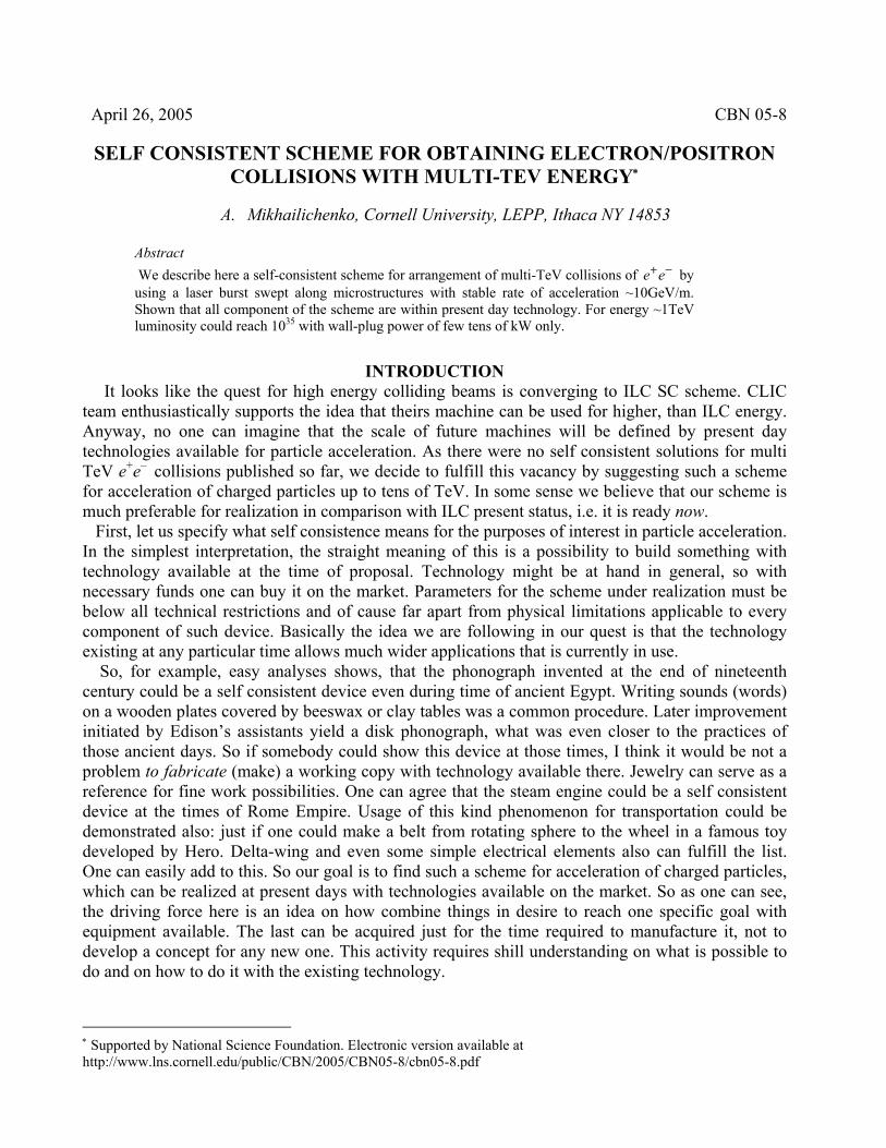
SWEEPING DEVICE For a prism-based device, Fig.3, change in refraction index yields the change in deflection angle. To arrange such a change, the basements of the prism must be covered by metallic foils and a high voltage applied to them.
Figure 3: The prism deflection device concept, left. Cross marks direction of optical axis. At the right- prisms with oppositely directed optical axes installed in series between two parallel strip–line electrodes, Electromagnetic pulse
)/( cytEx − propagates with laser bunch to the right. For a prism-based device, Fig.3, left, the deflecting angle is defined by the phase delay across the laser beam front arising from differences in the path lengths in material of the prism having a refractive index n
wLLn ba )( −
≅ϑ , (1)
where w~a –is the width of incident laser beam, La and Lb –are the distances through which the edges of the laser beam traverse the prism, Fig.3. A change in refractive index value yields a deflection angle change. If the basements of the prism are covered by metallization, then voltage V(t) applied to the metallization will change refractive index as∆ ∆n n V t= ( ( )) , so
wLLtnt ba )()()( −
≅ ∆ϑ∆ . (2)
The number of resolvable sports for this device N R can be found now as
λ∆
λ∆
λϑ∆ ln
LLnw
N baR ≅
−⋅=≅
/, (3)
where ba LLl −= stands for the prism base length and 1/ ≅wa in our case. In any case, a shorter wavelength is preferable from this point of view. One can see from (2) and (3) that with the increase in optic path difference l, both the deflection angle and the number of resolved spots increase also. To increase the last numbers the multiple-prism deflectors were developed, see Fig.3, right. Here neighboring prismatic crystals have oppositely oriented optical axes. These crystals positioned between the strip–line electrodes. In this case the full length of a sweeping device Ld serves as l in formulas (2), (3). To be able to sweep short laser bunches, the voltage pulse V (t) is propagating along this strip-line as a traveling wave together with the laser bunch to be swept, as it was proposed in [3]. This gives the necessary voltage profile along the laser pulse at cm distances, what corresponds to the pulse duration ~ cτ , which is ~100ps typically [2], [3].
6
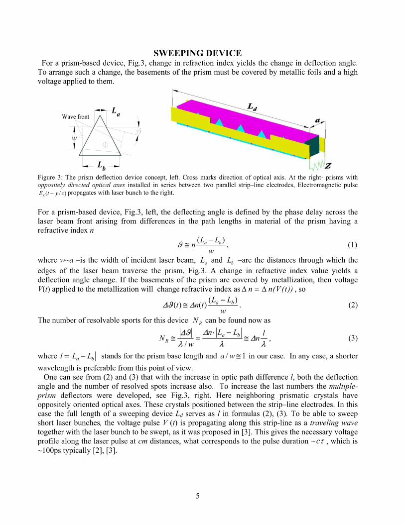
Figure 4: Laser pulse and EM driving wave propagating in the same direction.
The deflection angle and the number of resolved spots for such device become
)()( 302 tVrn
aL
wLtn ij
dd ⋅⋅≅≅ ∆ϑ∆ , max30max
max 2/
VrnLLnw
N ijdd
R ∆λλ
∆λϑ∆
==≅ , (4)
where Ld stands for full length of deflecting device, w–is the laser beam width (along direction of deflection), maxϑ∆ stands for full variation of deflection angle and electrical field substituted as
aVE /= . For Ld=25cm, one can expect for ≅≅ aw 0.5 cm, that deflection angle is ∆ϑ ≅ −10 2 and ≅RN 20 for λ µ≅ 10 m and, respectively ∆ϑ ≅ −10 2 and ≅RN 200 for λ µ≅ 1 m .
We estimated the field amplitude applied to the crystals as 10 kV/cm. This is really a field strength variation along the laser bunch. This variation is traveling together with the laser beam along the sweeping device, Fig. 4. For acceleration in one section, the laser flash energy passing through the single deflection system is ~0.1mJ. We estimated the area cowered by the laser beam as S w d≅ ⋅ , what is about 0.25cm2. This yields the energy density 0.3 mJ/ cm2 only. One can decrease the area up to 1000 times. Reduction of orthogonal dimension will reduce the power required for deflection. For such a sweeping device, a lot of electro-optical crystals can be used, see Table 1 below. For example, a crystal KDP (KH PO2 4 ) is transparent for a radiation with the wavelength λ ≅ 0.2÷1 µ m. Some other crystals, such as CdTe, CuCl, GaAs, ZnTe, and ZnS are transparent in the region of wavelengths around λ ≈ 10 µm . The last group of materials have rather high refractive indexes n0~(2-4) what compensate smaller electro- optical coefficient.
TABLE 1: Electro-optical materials for deflector
Wavelength Materials ϑ , rad NR
λ µ≅ 10 m GaAs, ZnTe, ZnS, CdS, CdTe, CuCl 0.01-0.02 20
λ µ≅ 5 m LiNbO3, LiTaO3, CuCl 0.01-0.02 40
λ µ≅ 1 m KDP, DKDP, ADP, KDA, LiNbO3 0.01-0.02 200
Despite the materials transparent for longer wavelengths have lower value of rij –components, they have higher values of refracting index, so the variation of refractive index becomes about the same.
7
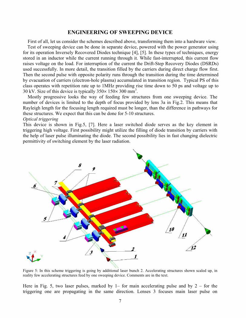
ENGINEERING OF SWEEPING DEVICE First of all, let us consider the schemes described above, transforming them into a hardware view. Test of sweeping device can be done in separate device, powered with the power generator using for its operation Inversely Recovered Diodes technique [4], [5]. In these types of techniques, energy stored in an inductor while the current running through it. While fast-interrupted, this current flow raises voltage on the load. For interruption of the current the Drift-Step Recovery Diodes (DSRDs) used successfully. In more detail, the transition filled by the carriers during direct charge flow first. Then the second pulse with opposite polarity runs through the transition during the time determined by evacuation of carriers (electron-hole plasma) accumulated in transition region. Typical PS of this class operates with repetition rate up to 1MHz providing rise time down to 50 ps and voltage up to 30 kV. Size of this device is typically 350× 150× 300 mm3. Mostly progressive looks the way of feeding few structures from one sweeping device. The number of devices is limited to the depth of focus provided by lens 3a in Fig.2. This means that Rayleigh length for the focusing length required must be longer, than the difference in pathways for these structures. We expect that this can be done for 5-10 structures. Optical triggering This device is shown in Fig.5, [7]. Here a laser switched diode serves as the key element in triggering high voltage. First possibility might utilize the filling of diode transition by carriers with the help of laser pulse illuminating the diode. The second possibility lies in fast changing dielectric permittivity of switching element by the laser radiation.
Figure 5: In this scheme triggering is going by additional laser bunch 2. Accelerating structures shown scaled up, in reality few accelerating structures feed by one sweeping device. Comments are in the text. Here in Fig. 5, two laser pulses, marked by 1– for main accelerating pulse and by 2 – for the triggering one are propagating in the same direction. Lenses 3 focuses main laser pulse on
8
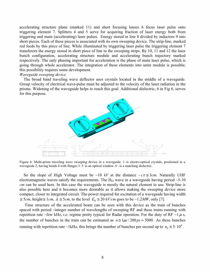
accelerating structure plane (marked 11) and short focusing lenses 6 focus laser pulse onto triggering element 7. Splitters 4 and 5 serve for acquiring fraction of laser energy both from triggering and main (accelerating) laser pulses. Energy stored in line 8 divided by inductors 9 into short pieces. Each of these pieces is associated with its own sweeping device. The strip-line, marked red feeds by this piece of line. While illuminated by triggering laser pulse the triggering element 7 transferees the energy stored in short piece of line to the sweeping strips. By 10, 11 and 12 the laser bunch configuration, accelerating structure module and accelerating bunch trajectory marked respectively. The only phasing important for acceleration is the phase of main laser pulse, which is going through whole accelerator. The integration of these elements into unite module is possible; this possibility requires some development. Waveguide sweeping device The broad band traveling wave deflector uses crystals located in the middle of a waveguide. Group velocity of electrical wave-pulse must be adjusted to the velocity of the laser radiation in the prisms. Widening of the waveguide helps to reach this goal. Additional dielectric, 6 in Fig 6, serves for this purpose.
Figure 6: Multi-prism traveling wave sweeping device in a waveguide. 1–is electro-optical crystals, positioned in a waveguide 2, having bends 4 with flanges 3. 5–is an optical window. 6 –is a matching dielectric.
So the slope of High Voltage must be ~10 kV at the distance ~ ≅τc 3cm. Naturally UHF electromagnetic waves satisfy the requirements. The H01 wave in a waveguide having period ~5-10 cm can be used here. In this case the waveguide is mostly the natural element to use. Strip-line is also possible here and it becomes more desirable as it allows making the sweeping device more compact, closer to integrated circuit. The power required for excitation of a waveguide having width ≅ 5cm, height≅ 1cm, λ ≅ 5cm, to the level 0E ≅ 20 kV/cm goes to be ~1.2MW, only [7]. Time structure of the accelerated beam can be seen with this device as the train of bunches spaced with period ~integer number of wavelengths of sweeping RF and these trains running with repetition rate ~few kHz, i.e. regime pretty typical for Radar operation. For the duty of RF ~1µ s, the number of bunches in the train can be estimated as 5000200/1 =≅ pssn µ . As these bunches running with repetition rate ~1kHz, this brings the number of bunches per second up to 6105 ⋅≅bn .
9
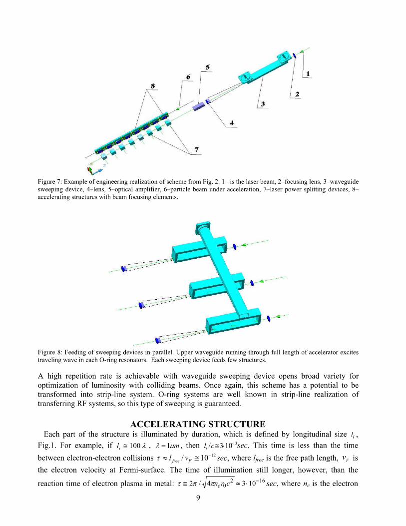
Figure 7: Example of engineering realization of scheme from Fig. 2. 1 –is the laser beam, 2–focusing lens, 3–waveguide sweeping device, 4–lens, 5–optical amplifier, 6–particle beam under acceleration, 7–laser power splitting devices, 8–accelerating structures with beam focusing elements.
Figure 8: Feeding of sweeping devices in parallel. Upper waveguide running through full length of accelerator excites traveling wave in each O-ring resonators. Each sweeping device feeds few structures. A high repetition rate is achievable with waveguide sweeping device opens broad variety for optimization of luminosity with colliding beams. Once again, this scheme has a potential to be transformed into strip-line system. O-ring systems are well known in strip-line realization of transferring RF systems, so this type of sweeping is guaranteed.
ACCELERATING STRUCTURE
Each part of the structure is illuminated by duration, which is defined by longitudinal size tl , Fig.1. For example, if λ100≅tl , mµλ 1= , then 13103/ −⋅≅clt sec. This time is less than the time between electron-electron collisions 1210/ −≅≈ Ffree vlτ sec, where lfree is the free path length, vF is the electron velocity at Fermi-surface. The time of illumination still longer, however, than the
reaction time of electron plasma in metal: 1620 1034/2 −⋅≈≅ crneππτ sec, where ne is the electron
10
density in a metal. Even doped semiconductor can be fast enough react to laser radiation. The tunneling probability brings a limit to the surface field as high as eUE
F/4 2
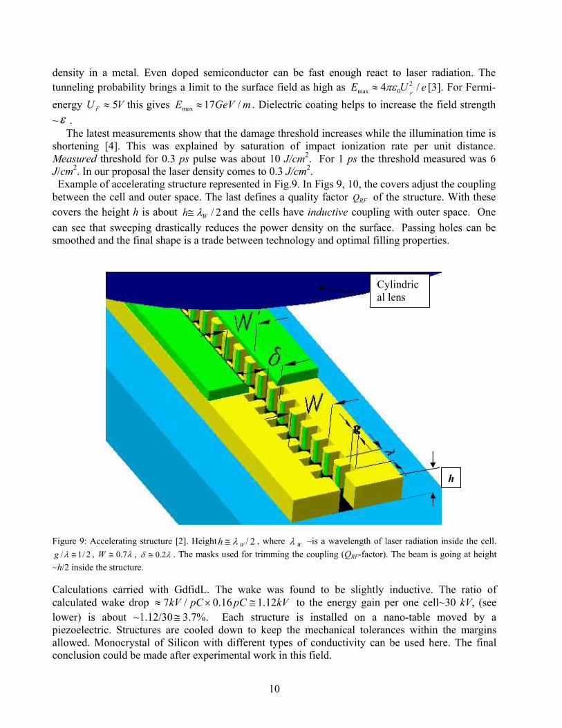
0max πε≈ [3]. For Fermi-energy VU F 5≈ this gives mGeVE /17max ≈ . Dielectric coating helps to increase the field strength ~ ε . The latest measurements show that the damage threshold increases while the illumination time is shortening [4]. This was explained by saturation of impact ionization rate per unit distance. Measured threshold for 0.3 ps pulse was about 10 J/cm2. For 1 ps the threshold measured was 6 J/cm2. In our proposal the laser density comes to 0.3 J/cm2. Example of accelerating structure represented in Fig.9. In Figs 9, 10, the covers adjust the coupling between the cell and outer space. The last defines a quality factor RFQ of the structure. With these covers the height h is about 2/Wh λ≅ and the cells have inductive coupling with outer space. One can see that sweeping drastically reduces the power density on the surface. Passing holes can be smoothed and the final shape is a trade between technology and optimal filling properties.
Figure 9: Accelerating structure [2]. Height h W≅ λ / 2 , where λ W –is a wavelength of laser radiation inside the cell. 2/1/ ≅λg , λ7.0≅W , λδ 2.0≅ . The masks used for trimming the coupling (QRF-factor). The beam is going at height
~h/2 inside the structure. Calculations carried with GdfidL. The wake was found to be slightly inductive. The ratio of calculated wake drop kVpCpCkV 12.116.0/7 ≅×≈ to the energy gain per one cell~30 kV, (see lower) is about ~1.12/30≅ 3.7%. Each structure is installed on a nano-table moved by a piezoelectric. Structures are cooled down to keep the mechanical tolerances within the margins allowed. Monocrystal of Silicon with different types of conductivity can be used here. The final conclusion could be made after experimental work in this field.
Cylindrical lens
h
11
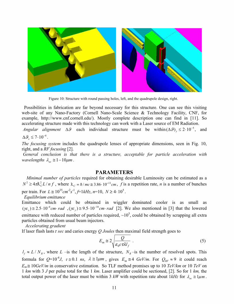
Figure 10: Structure with round passing holes, left, and the quadrupole design, right. Possibilities in fabrication are far beyond necessary for this structure. One can see this visiting web-site of any Nano-Factory (Cornell Nano-Scale Science & Technology Facility, CNF, for example, http://www.cnf.cornell.edu/). Mostly complete description one can find in [11]. So accelerating structure made with this technology can work with a Laser source of EM Radiation. Angular alignment ϑ∆ each individual structure must be within 5102)( −⋅≤∆ yϑ , and
4107 −⋅≤∆ xϑ . The focusing system includes the quadrupole lenses of appropriate dimensions, seen in Fig. 10, right, and a RF focusing [2]. General conclusion is that there is a structure, acceptable for particle acceleration with wavelengths mac µλ 101−≅ .
PARAMETERS Minimal number of particles required for obtaining desirable Luminosity can be estimated as a
fnLN C /4 22 Dπ≥ , where cmmcC111086.3/ −⋅≅= hD , f is a repetition rate, n is a number of bunches
per train. For ≅L 1035cm-2s-1, f=1kHz, n=10, 5104 ⋅≥N . Equilibrium emittance Emittance which could be obtained in wiggler dominated cooler is as small as
radcmx ⋅⋅≅ −8105.2)(γε , radcmy ⋅⋅≅ −10105.9)(γε [2]. We also mentioned in [3] that the lowered emittance with reduced number of particles required, ~105, could be obtained by scrapping all extra particles obtained from usual beam injectors. Accelerating gradient If laser flash lastsτ sec and caries energy Q Joules then maximal field strength goes to
fm lc
QEτλε 0
2≅ . (5)
l L Nf R≈ / , where L –is the length of the structure, RN –is the number of resolved spots. This formula for Q=10-4J, τ ≅ 0.1 ns, mµλ 1≅ , gives ≅mE 4 GeV/m. For 9≈RFQ it could reach Em≅ 10GeV/m in conservative estimation. So TLF method promises up to 10 TeV/km or 10 TeV on 1 km with 3 J per pulse total for the 1 km. Laser amplifier could be sectioned, [2]. So for 1 km, the total output power of the laser must be within 3 kW with repetition rate about 1kHz for mac µλ 1≅ .

12
Nd-Glass lasers can be used here. For pumping the driving lasers the diode laser arrays (efficiency ~30%) could be used for the wavelengths indicated. This brings efficiency of the laser up to 10% level. Bunch population Considering the balance of energy, accepted from the field, one can obtain for N estimation
f
ac
lcQ
geIN
τλεη 3
0
)(2≅ . (6)
)(gI –an analog of the transit time factor, With I(g )= 0.7, ≈η 0.05 (i.e. only 5% of energy stored in one cell carried out by the bunch), this yields N 5103 ⋅≅ for mac µλ 1≅ . Luminosity Formula for luminosity yxBfHNL σπσ4/2= , where f –is a repetition rate, yx,σ are the Gaussian widths for x and y directions respectively, HB – is the enhancement parameter. BN –is the number of bunches per train, gives for radcmx ⋅⋅≅ −8105.2γε , radcmx ⋅⋅≅ −10105.9γε and for
acyx λββ 3.0≈≈ , mac µλ 1≅ , 6102 ⋅=γ (pc=1TeV), 5103 ⋅≅N , ≅f 1 kHz, HB=1, NB=1 the value 1235107.1 −−⋅≈ scmL . For mac µλ 10≅ result will be about the same. The transverse Gaussian size
will be cmxxx9101.1/*)( −⋅≅≅ πγβγεσ and cmy
10102.2 −⋅≅σ . So the aspect ratio in this case is about ≅yx σσ / 5, what looks reasonable. Operation with high repetition rate, up to tens of MHz is possible here, drastically reducing the number of particles required. Radiation at IP Radiation can be characterized by Y0 parameter, cc HHEY /3/20 γω =≡ h , where H is the magnetic field, 1332 104.4/ ⋅≅= hecmHc G, ω c is critical frequency of classical synchrotron radiation. For E~1TeV, this parameter goes to be ~103. Formation length for the boundary particles goes to )/( 3/2
0 bCF Yl σγD≅ . Critical energy of radiated photons goes to 02 /Ymcc γω ≅h , and
corresponding wavelength is γω 20 // mccYc ccr hD =≅ . So the transverse size of coherence goes to
CbFcrcoh Yl DD 6/1
0≅≅⊥ σσ ~ cmC101015.13 −⋅≅D . So the radiation from the incoming bunch
formally could not be described as a dipole radiation of a single particle in coherent field of oncoming bunch. In this case the particles on opposite vertical sides of the bunch have opposite accelerations. This yield opposite polarizations of electromagnetic fields, radiated by these oppositely located particles. In it’s turn this yields a destructive interference of radiation in forward direction. So the resulting radiation looks like a quadrupole one. This type of radiation has zero intensity in forward direction. For peripheral coordinate the size Nyx /,σσ ≡⊥ , where N –is a bunch population, needs to be taken for estimations of magnetic field strength. So the radiation is strongly suppressed here N/1~ . This is a peculiarity of a laser driven accelerator [3]. Radiation in final lens Effect of synchrotron radiation in a quadrupole lens was considered first in [8]. In [9] there was considered focusing in plasma with adiabatically changing strength for reduction of final quad phenomena. We suggested an arrangement of the final focus as a multiplet of FODO arranged with RF structures. The number of (RF) lenses in such a multiplet ≈ 103 [2]. We extend the name Adiabatic Final Focus to this device also. The gradient in these RF lenses varies from very strong at the side closest to IP, to a weak one at opposite side. For 1 TeV, according to calculations done in

13
[3], the focusing parameter k could be as big as 103 1/m2. Focal distance F goes to be 2001051011 63 =⋅⋅≅≅ −kgF [Meters/cell] (g-from Fig.9). So the lens with ≈ 103 cells reaches
the focal distance F≈ 20 cm. Let just remind that these cells will occupy 0.1 cm only.
GENERAL SCHEME
General scheme represented in Fig.11 below. It looks traditional pretty much.
+ +2 1 km /2 10 TeV
Figure 11: Laser Linear Collider (LLC) complex. 1–is a laser master oscillator platform, 2 –is an optical splitter, 3,4–are the mirrors, 5–is a semi-transparent mirror, 6–is an absorber of laser radiation. 7–are the Final Focus Systems. 8–are the damping systems for preparing particle’s beams with small emittances, 9–are the isochronous bends for the particle’s beam. 10–are the accelerating X-band structures, 11–is an electron gun, 12–is a positron converter. The scheme with the damping rings as sources are shown here. The laser and particle’s bunch run first apart from the IP. On this way all parameters (laser, electron/positron) picked up, processed with appropriate algorithms locally and applied to correcting elements on the back way to IP. One can imagine that LLC has two stages with two wavelengths. Small crossing angle required for preventing illumination of the final lenses by used beam. Repetition rate up to few kHz, allows easy manipulation with the beams. Interaction of beams at IP is going in deep quantum regime. The beams of electrons and positrons can be polarized what gives the effective gain in luminosity and reduces the background. For this purposes a helical undulator can be installed in the system. As the beam size can be made small, undulator period goes into mm level, coming to ~10 m total length. Neighboring platforms aligned with help of sensors, installed at the end of each platform. So the sensor installed at one platform touches neighboring one. The sensors are similar to that used in tunneling microscope technique. This system could be made fast enough to exclude influence of ground motion, mostly intensive at lower edge of the spectrum. Bunching arranged by energy modulation and following dispersive drift. For this purpose laser radiation co-propagating with the particles inside a wiggler having appropriate period. Multistage system with two laser frequencies suggested here, [3].
14
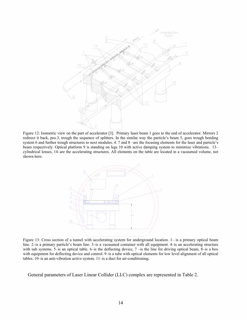
Figure 12: Isometric view on the part of accelerator [3]. Primary laser beam 1 goes to the end of accelerator. Mirrors 2 redirect it back, pos.3, trough the sequence of splitters. In the similar way the particle’s beam 5, goes trough bending system 6 and further trough structures to next modules, 4. 7 and 8 –are the focusing elements for the laser and particle’s beam respectively. Optical platform 9 is standing on legs 10 with active damping system to minimize vibrations. 13–cylindrical lenses, 14–are the accelerating structures. All elements on the table are located in a vacuumed volume, not shown here.
Figure 13: Cross section of a tunnel with accelerating system for underground location. 1– is a primary optical beam line. 2–is a primary particle’s beam line. 3–is a vacuumed container with all equipment. 4–is an accelerating structure with sub systems. 5–is an optical table. 6–is the deflecting device, 7 –is the line for driving optical beam, 8–is a box with equipment for deflecting device and control. 9–is a tube with optical elements for low level alignment of all optical tables. 10–is an anti-vibration active system. 11–is a duct for air-conditioning.
General parameters of Laser Linear Collider (LLC) complex are represented in Table 2.

15
Table 2: Parameters of collider
Wavelength mac µλ 1≅ Energy of e± beam 2× 10 TeV
Luminosity 1035cm-2s-1 Total two-linac length 2 × 1 km
Main linac gradient 10 GeV/m Bunch population 3 105
Bunch length 0.1 mµ No. of bunches/train 30
γ ε γ εx y/ radcm⋅⋅⋅ −− 99 101/105 Laser flash energy 2× 3J
Laser density 0.3 J/cm2
Illumination time 0.1 ps Length of section 3cm
Laser flash energy/section 100µJ Repetition rate 1 kHz
Laser beam power 2× 3kW Damping ring energy 2 GeV
Damping time 10ms Wall plug power** 2× 30 kW
** Without supplementary electronics.
CONCLUSION
Nano–technology available creates solid base for accelerator with Travelling Laser Focus. Illuminating time and total laser power reduction in this method defined by the number of resolved spots (pixels) associated with deflecting device. Lasers for the TLF method need to operate with ps100≈τ pulse duration. Any point on accelerating structure remains illuminated by ~0.3 ps only. TLF method promises up to 10 TeV/km with 3 mJ/m. With such high gradients, −+µµ , −+ππ ,
pp µπ , and ion-ion collisions become feasible. We conclude that acceleration in a laser-driven linac with TLF method is a present day technology and no physical and technical limitations found on this way. Testing of this method might be a highest priority task for accelerator physics.
REFERENCES
[1] A.A.Mikhailichenko, “The Method of Acceleration of Charged Particles”, Author’s certificate USSR N1609423, Priority May 1989, Bulletin of Inventions (in Russian), N6, p.220, 1994.
[2] A.A. Mikhailichenko, “Physical Foundations for Acceleration by Travelling Laser Focus”, Presented at AAC Workshop, Stony Brook, NY June 21-26, CBN 04-6. Electronic version available at http://www.lns.cornell.edu/public/CBN/2004/CBN04-6/phys_found.pdf
[3] A.A.Mikhailichenko, “Particle acceleration in Microstructures, Excited by Laser Radiation”, CLNS 00/1662, Cornell 2000; Also Snowmass 2001. Full list of referred can be found there. Electronic version available at http://www.lns.cornell.edu/public/CLNS/2000/
16
[4] D. Du, X. Lu, G. Korn, J. Squuier, G. Mourou, “Optical Breakdown with Femtosecond Laser Pulses”, CLEO94, May 8-13, 1994, Anaheim, California, Vol.8, p.407.
[5] I.V.Grekhov, V.M. Efanov, A.F. Kardo-Sysoev, S.V. Shenderei, Pis’ma Zh.Tech.Fiz., 1983, vol.9, no 7, p.435.
[6] I.V.Grekhov, V.M. Efanov, A.F. Kardo-Sysoev, S.V. Shenderei, Solid-State Electron., 1985, vol.28, no 6, p.597.
[7] A.A. Mikhailichenko, “Fast Sweeping Device for Laser Bunch”, CBN 05-6, Cornell University, LEPP, March 17, 2005. Electronic version is available at http://www.lns.cornell.edu/public/CBN/2005/CBN05-6/cbn05-6.pdf.
[8] V.L.Mikhalev, R.A.Rzaev, I.M.Ternov, “Motion of TeV-electrons in Quadrupole Magnetic Field allowing for Synchrotron Radiation”, Zh. Tech.Fiz. 52, 423-432(March 1982), Sov.Phys.Tech.Phys. 27(3), March 1982. Translation of American Institute of Physics.
[9] P.Chen, K.Oide, A.M.Sesler, S.S. Yu, “Plasma-Based Adiabatic Focuser”, Phys. Rev. Lett. 64(1231-1234), 12 March 1990.
[10] I.V.Grekhov, M.E. Levinstein, V.G. Sergeev, I.N.Yassievich, “Transient Characteristics of Semiconductor Switch, Triggered by Laser Pulse”, JETF, 1079, V. 49, N5, pp.1013-1021.
[11] Springer Handbook of Nano-Technology, Ed. Bhushan, ISBN 3-540-01218-4, 2004