self-assembly of complex multimetal nanostructures from ...snml.kaist.ac.kr/jou_pdf/183.pdf ·...
TRANSCRIPT

Self-Assembly of Complex Multimetal Nanostructures fromPerforated Lamellar Block Copolymer Thin FilmsSeung Keun Cha,† Gil Yong Lee,† Jeong Ho Mun,† Hyeong Min Jin,† Chang Yun Moon,† Jun Soo Kim,†
Kwang Ho Kim,*,‡ Seong-Jun Jeong,*,§ and Sang Ouk Kim*,†
†National Creative Research Initiative (CRI) Center for Multi-Dimensional Directed Nanoscale Assembly, Department of MaterialScience and Engineering, KAIST, Daejeon 34141, Republic of Korea‡Department of Materials Science and Engineering, Pusan National University, Pusan 46241, Republic of Korea§Device Laboratory, Device & System Research Center, Samsung Advanced Institute of Technology, Suwon 16678, Republic ofKorea
*S Supporting Information
ABSTRACT: We introduce a facile and effective fabrication of complexmultimetallic nanostructures through block copolymer self-assembly. Two- andthree-dimensional complex nanostructures, such as “nanomesh,” “double-layerednanomeshes,” and “surface parallel cylinders on nanomesh,” can be fabricatedusing the self-assembly of perforated lamellar morphology in block copolymerthin films. Simultaneous integration of various metallic elements, including Pt, Au,and Co, into the self-assembled morphologies generates multimetal complexnanostructures with highly interconnected morphology and a large surface. Theresultant metal nanostructures with a large surface area, robust electricalconnectivity, and well-defined alloy composition demonstrate a high-performanceelectrochemical catalysis for hydrogen evolution reaction (current density: 6.27mA/[email protected] V and Tafel slope: 43 mV/dec).
KEYWORDS: block copolymer, self-assembly, metal nanostructure, catalyst, hydrogen evolution
1. INTRODUCTION
Nanoscale self-assembly offers enormous potential for highlyefficient scalable nanofabrication.1−6 Functional nanopatternstructures prepared using the self-assembly principle can beuseful for a broad spectrum of application fields, includingelectronics, photonics, sensors, and energy storage/conver-sion.7−11 Block copolymer (BCP) self-assembly is a well-established representative self-assembly principle, which hasbeen widely exploited for nanopatterning applications partic-ularly aiming at semiconductor device fabrication.12−21 Itprovides dense periodic arrays of self-assembled nanodomainswith a typical characteristic dimension of 3−50 nm.13,22−27 Incontrast to the sphere, cylinder, or lamellar self-assembledmorphology commonly used for line or dot array patterning,perforated lamellar (PL) phase, known to be metastable in bulkphase, can be stabilized in thin films.28−31 Knoll et al. reportedthat cylinder-forming BCP thin films generated PL structuresunder specific conditions because of an interplay between thesurface field and confinement effects.30 Lyakhova et al.demonstrated that various structures including the PL phasewere found in BCP thin films, resulting from the differentsurface fields of the two interfaces.31 Such a PL morphologymay provide densely ordered nanoporous structures, which canbe used as a template for the complex nanoporous structureformation, such as membranes.32
In this work, we demonstrate a simple and effective self-assembly of multimetal complex nanoporous structures with aninterconnected morphology using a PL BCP self-assembly.Various nanoporous structures including two-dimensional (2D)nanomesh to three-dimensional (3D) nanocomplex structurescan be stabilized in BCP thin films by judicious control of thefilm thickness and interfacial energy. Subsequently, highlyspecific incorporation of metallic precursors into self-assembledhydrophilic nanodomains generates multimetal complexnanostructures. Among various resultant metal nanostructures,Pt nanomesh was used as a model catalyst for the electro-chemical hydrogen evolution reaction (HER). Owing to thehighly interconnected reliable electrical pathway and largeenough surface area, Pt nanomesh catalysts exhibit an improvedHER performance than the flat Pt catalysts and are at a levelsimilar to the Tafel slope of commercial Pt/C catalysts.
2. EXPERIMENTAL SECTION2.1. Fabrication of Monolayer Metal Nanomesh Patterns.
Polystyrene-block-poly(2-vinylpyridine) (PS-b-P2VP; Mn = 18 kg/molfor PS and 9 kg/mol for P2VP) was purchased from Polymer Source,Inc. PS-b-P2VP was dissolved in toluene (Sigma-Aldrich) to prepare
Received: March 8, 2017Accepted: April 12, 2017Published: April 12, 2017
Research Article
www.acsami.org
© 2017 American Chemical Society 15727 DOI: 10.1021/acsami.7b03319ACS Appl. Mater. Interfaces 2017, 9, 15727−15732
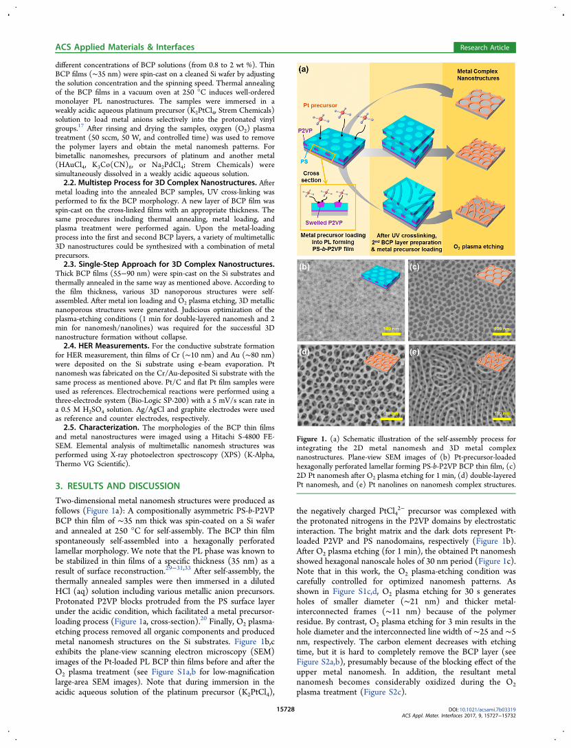
different concentrations of BCP solutions (from 0.8 to 2 wt %). ThinBCP films (∼35 nm) were spin-cast on a cleaned Si wafer by adjustingthe solution concentration and the spinning speed. Thermal annealingof the BCP films in a vacuum oven at 250 °C induces well-orderedmonolayer PL nanostructures. The samples were immersed in aweakly acidic aqueous platinum precursor (K2PtCl4, Strem Chemicals)solution to load metal anions selectively into the protonated vinylgroups.17 After rinsing and drying the samples, oxygen (O2) plasmatreatment (50 sccm, 50 W, and controlled time) was used to removethe polymer layers and obtain the metal nanomesh patterns. Forbimetallic nanomeshes, precursors of platinum and another metal(HAuCl4, K3Co(CN)6, or Na2PdCl4; Strem Chemicals) weresimultaneously dissolved in a weakly acidic aqueous solution.2.2. Multistep Process for 3D Complex Nanostructures. After
metal loading into the annealed BCP samples, UV cross-linking wasperformed to fix the BCP morphology. A new layer of BCP film wasspin-cast on the cross-linked films with an appropriate thickness. Thesame procedures including thermal annealing, metal loading, andplasma treatment were performed again. Upon the metal-loadingprocess into the first and second BCP layers, a variety of multimetallic3D nanostructures could be synthesized with a combination of metalprecursors.2.3. Single-Step Approach for 3D Complex Nanostructures.
Thick BCP films (55−90 nm) were spin-cast on the Si substrates andthermally annealed in the same way as mentioned above. According tothe film thickness, various 3D nanoporous structures were self-assembled. After metal ion loading and O2 plasma etching, 3D metallicnanoporous structures were generated. Judicious optimization of theplasma-etching conditions (1 min for double-layered nanomesh and 2min for nanomesh/nanolines) was required for the successful 3Dnanostructure formation without collapse.2.4. HER Measurements. For the conductive substrate formation
for HER measurement, thin films of Cr (∼10 nm) and Au (∼80 nm)were deposited on the Si substrate using e-beam evaporation. Ptnanomesh was fabricated on the Cr/Au-deposited Si substrate with thesame process as mentioned above. Pt/C and flat Pt film samples wereused as references. Electrochemical reactions were performed using athree-electrode system (Bio-Logic SP-200) with a 5 mV/s scan rate ina 0.5 M H2SO4 solution. Ag/AgCl and graphite electrodes were usedas reference and counter electrodes, respectively.2.5. Characterization. The morphologies of the BCP thin films
and metal nanostructures were imaged using a Hitachi S-4800 FE-SEM. Elemental analysis of multimetallic nanomesh structures wasperformed using X-ray photoelectron spectroscopy (XPS) (K-Alpha,Thermo VG Scientific).
3. RESULTS AND DISCUSSION
Two-dimensional metal nanomesh structures were produced asfollows (Figure 1a): A compositionally asymmetric PS-b-P2VPBCP thin film of ∼35 nm thick was spin-coated on a Si waferand annealed at 250 °C for self-assembly. The BCP thin filmspontaneously self-assembled into a hexagonally perforatedlamellar morphology. We note that the PL phase was known tobe stabilized in thin films of a specific thickness (35 nm) as aresult of surface reconstruction.29−31,33 After self-assembly, thethermally annealed samples were then immersed in a dilutedHCl (aq) solution including various metallic anion precursors.Protonated P2VP blocks protruded from the PS surface layerunder the acidic condition, which facilitated a metal precursor-loading process (Figure 1a, cross-section).20 Finally, O2 plasma-etching process removed all organic components and producedmetal nanomesh structures on the Si substrates. Figure 1b,cexhibits the plane-view scanning electron microscopy (SEM)images of the Pt-loaded PL BCP thin films before and after theO2 plasma treatment (see Figure S1a,b for low-magnificationlarge-area SEM images). Note that during immersion in theacidic aqueous solution of the platinum precursor (K2PtCl4),
the negatively charged PtCl42− precursor was complexed with
the protonated nitrogens in the P2VP domains by electrostaticinteraction. The bright matrix and the dark dots represent Pt-loaded P2VP and PS nanodomains, respectively (Figure 1b).After O2 plasma etching (for 1 min), the obtained Pt nanomeshshowed hexagonal nanoscale holes of 30 nm period (Figure 1c).Note that in this work, the O2 plasma-etching condition wascarefully controlled for optimized nanomesh patterns. Asshown in Figure S1c,d, O2 plasma etching for 30 s generatesholes of smaller diameter (∼21 nm) and thicker metal-interconnected frames (∼11 nm) because of the polymerresidue. By contrast, O2 plasma etching for 3 min results in thehole diameter and the interconnected line width of ∼25 and ∼5nm, respectively. The carbon element decreases with etchingtime, but it is hard to completely remove the BCP layer (seeFigure S2a,b), presumably because of the blocking effect of theupper metal nanomesh. In addition, the resultant metalnanomesh becomes considerably oxidized during the O2plasma treatment (Figure S2c).
Figure 1. (a) Schematic illustration of the self-assembly process forintegrating the 2D metal nanomesh and 3D metal complexnanostructures. Plane-view SEM images of (b) Pt-precursor-loadedhexagonally perforated lamellar forming PS-b-P2VP BCP thin film, (c)2D Pt nanomesh after O2 plasma etching for 1 min, (d) double-layeredPt nanomesh, and (e) Pt nanolines on nanomesh complex structures.
ACS Applied Materials & Interfaces Research Article
DOI: 10.1021/acsami.7b03319ACS Appl. Mater. Interfaces 2017, 9, 15727−15732
15728

For the formation of 3D metal complex nanostructures, suchas “double-layered metal nanomeshes” or “nanolines onnanomesh”, a multistep process was used (see the illustrationin Figure 1a). First, Pt-loaded monolayer PL-forming PS-b-P2VP BCP samples were prepared as described above andcross-linked using UV light to preserve the nanoscale structureduring the following overlay process. Subsequently, the secondPS-b-P2VP BCP layer was prepared in the same way over thecross-linked first layer. The phase morphology of the secondlayer was delicately dependent on the film thickness. Typically,the second BCP thin films with thicknesses of 35 and 30 nmwere deposited, where PL and surface parallel cylinder phaseswere formed, respectively. After the second Pt-loading process,the polymer template was completely removed by O2 plasmaetching. The resultant 3D Pt nanocomplex structures with a Ptnanomesh bottom layer are shown in Figure 1d,e. Plane-viewSEM images reveal that the underlying Pt nanomesh layers arewell-maintained and intact. The hole diameter and theinterconnected line width of the double-layered Pt nanomeshstructure were ∼25 and ∼5 nm (Figure 1d), respectively, andthe Pt line width in the Pt nanoline/nanomesh complex was 5nm (Figure 1e). This multistep approach can be furtherrepeated for obtaining thicker 3D nanoporous structures.Three-dimensional metal complex nanostructures could also
be obtained by a single-step deposition of BCP films with aprecisely controlled thickness (see the illustration in Figure 2a).
Compositionally asymmetric BCP thin films enable variousnanostructures, including wetting layer (dis), spherical micro-domains, a PL, and cylinders (C⊥ or C∥), as a result of thesurface reconstruction modulated by interference and confine-ment effects.30,33 Interestingly, PS-b-P2VP BCP thin films (Mn= 18 kg/mol for PS and 9 kg/mol for P2VP) with thethicknesses of ∼35 and ∼60 nm demonstrated single- anddouble-layered PL phases, respectively (Figure 2b). When thefilm thickness was ∼83 nm, a “double-layered surface parallel
cylinder/PL complex phase” was observed, which may bestrongly influenced by the thickness commensurability andsurface/interfacial energies. As shown in Figure 2c, the self-assembled BCP nanostructure consisted of a cylindrical bottomlayer and a PL top layer, where the Si substrate waspreferentially wetted by P2VP blocks. The morphologiesshown in Figure 2b,c are 3D Pt complex nanostructures afterPt ion loading and O2 plasma etching. The O2 plasma-etchingtime was also carefully controlled (for “double-layered Ptnanomeshes” and “nanoline/nanomesh”, O2 plasma-etchingtimes were 1 and 2 min, respectively). A brief etching for lessthan 1 min was not enough to reveal the bottomnanostructures, and a long etching for over 3 min destroyedthe 3D complex nanostructures (Figure S3).The perforated P2VP lamellar phase is an attractive
nanotemplate for highly interconnected multimetal nanostruc-tures. Figure 3 shows the plane-view SEM images of bimetallic
nanomeshes produced by the simultaneous incorporation oftwo different metal precursors (of Pt−Au, Pt−Pd, or Pt−Co).Interestingly, when a single precursor of Au, Pd, or Co wasloaded without Pt precursor, the resultant morphologies readilycollapsed (Figure 3b,e,h). By contrast, pure Pt nanomeshshowed an excellent morphological stability (Figures 1 and 2).This can be attributed to a high loading density of Pt precursor
Figure 2. (a) Schematic illustration of the single-step process for 3Dmetal nanostructures, based on the precise control of BCP filmthickness for surface reconstruction. Plane-view SEM images of (b)double-layered Pt nanomesh structures after O2 plasma etching for 1min and (c) Pt nanomesh on Pt lines after O2 plasma etching for 2min.
Figure 3. (a) Schematic procedure of bimetallic nanomeshes throughsimultaneous loading of two different metallic precursors. Plane-viewSEM images of metal nanomeshes according to the relativecompositions of different metals (Pt−Au, Pt−Pd, or Pt−Co) at 0mol % Pt (b,e,h), at 25 mol % Pt (c,f,i), and at 50 mol % Pt (d,g,j),respectively.
ACS Applied Materials & Interfaces Research Article
DOI: 10.1021/acsami.7b03319ACS Appl. Mater. Interfaces 2017, 9, 15727−15732
15729

into BCP templates with a strong agglomeration behavior. Asshown in Figure S4, Pt nanodots showed densely agglomeratedmorphologies with small diameters (13−15 nm). By contrast,Pd (15−18 nm) and Au dots (16−20 nm) showed coarselypacked nanocluster morphologies with larger diameters, whichindicates that the loaded metal patterns do not exactly followthe BCP nanotemplate. Co anions were not loaded into theBCP template enough, so the resultant Co dot pattern wasunclear with many defects. These results demonstrate that Pt isa good metal element to maintain the entire nanopatterns ofBCP films, enabling the stable nanomesh morphology duringthe metal-loading and plasma-etching processes. As a result,when the Pt composition was above 50 mol % in themultimetallic nanostructure formation, the morphologicalstability was significantly improved (Figure 3d,g,j). The exactchemical compositions of the bimetallic nanomeshes wereconfirmed using XPS analysis (Figure S5 and Table 1). Thefabricated bimetallic nanomeshes were composed of Pt (38 at%)−Au (62 at %), Pt (56 at %)−Pd (44 at %), and Pt (79 at%)−Co (21 at %).
Multimetal complex 3D nanostructures could be accom-plished by multistep repetition of BCP self-assembly andmetallization cycles (see Figure 4a). First, precursors of Pt andanother metal were loaded into the first self-assembled PL BCPlayers. Subsequently, the samples were illuminated using UVlight for morphology fixing by chemical cross-linking. Thesecond BCP layer was overlaid upon the cross-linked BCP layerby spin-coating and thermally annealed for self-assembly. Asubsequent metal-loading process with precursors of Pt and athird metal and O2 plasma treatment achieved 3D multimetalcomplex nanostructures. Figure 4b,c shows the plane-view SEMimages of “double-layered nanomeshes” with a Pt−Co top layerand a Pt−Pd bottom layer and with a Pt−Au top layer and aPt−Co bottom layer, respectively. The chemical composition ofthe multimetal complex nanostructures was also confirmedusing the XPS analysis (Figures 4d and S6). The fabricatedtrimetallic complex nanostructure were composed of Pt (52.8 at%)−Pd (33.8 at %)−Co (13.4 at %) and Pt (53.7 at %)−Co(26.9 at %)−Au (19.4 at %) (Table S1). To confirm thecontamination possibility of the preceding lower layer duringthe subsequent metal-loading process, we prepared a Pt-precursor-loaded PS-b-P2VP BCP film. After its cross-linkingand immersion into a Co precursor solution, its metalnanomesh was carefully analyzed using XPS. Note that itspolymer part was sufficiently removed by O2 plasma beforeXPS analysis. As shown in Figure S7, we have not found thesecond metal element (Co) other than the first metal element(Pt) in the metal nanomesh within the detection limit. Theresult clearly demonstrates that the metal-loading processes weused enabled the multimetal complex nanomesh structureswithout any contaminations between each layer. It may be dueto the weak interaction between metal anions and cross-linkedP2VP blocks. These results elucidate that our scalable approach
successfully achieved 3D multimetal complex nanostructureswhile maintaining the different underlying bimetallic nano-meshes. Note that we could also fabricate the multimetalcomplex nanostructures based on nanolines on nanomesh witha Pt−Co−Pd alloy (see Figure S8).Finally, we recorded the electrochemical HER measurements
using a three-electrode setup under an acidic solution conditionto characterize the HER catalyst performance of the fabricatedmetallic nanomesh structures. Hydrogen has been attractingenormous research attention as a promising alternative energycarrier. To date, various catalyst materials have been exploitedto maximize the energy conversion efficiency. In this work, ahighly interconnected Pt nanomesh with a large surface areawas used as the HER catalyst. As a reference for HERperformance, a commercial Pt/C catalyst and a flat Pt film werealso characterized. Figure 5 shows the typical polarizationcurves (I−V plot) and the Tafel plots of the three samples.Although the commercial Pt/C catalyst showed the highestHER performance, the improved HER performance of Ptnanomesh was also demonstrated (current density of Pt/C =17.5 mA/[email protected] V, Ptnanomesh = 6.27 mA/[email protected] V, andPtflat = 1.04 mA/[email protected] V). The Tafel slope of the Ptnanomesh was at a level similar to that of Pt/C catalyst [Tafelslope (T) of the three samples: T(Pt/C) = 36 mV/dec,T(Pt nanomesh) = 43 mV/dec, and T(flat Pt film) = 85 mV/dec].These superior HER performances of Pt nanomesh could beattributed to the highly connected robust electrical pathway andthe large active catalytic surface area of the nanomesh structure.
Table 1. Composition of Bimetallic Nanomeshes of Pt−Au,Pt−Pd, and Pt−Co Analyzed Using XPSa
element composition of Pt (at %) composition of second metal (at %)
Pt−Au 38 62Pt−Pd 56 44Pt−Co 79 21
aThe molar ratio between the two precursors is 1/1.
Figure 4. (a) Schematic procedure of the fabrication of 3D multimetalcomplex nanomeshes through the multistep process. SEM images of3D multimetallic nanomeshes with the elements of (b) Pt−Pd−Co(bottom Pt−Pd and top Pt−Co) and (c) Pt−Co−Au (bottom Pt−Coand top Pt−Au). (d) XPS spectra of the Pt−Pd−Co multimetallicnanomesh double layer (b).
ACS Applied Materials & Interfaces Research Article
DOI: 10.1021/acsami.7b03319ACS Appl. Mater. Interfaces 2017, 9, 15727−15732
15730

4. CONCLUSIONS
We have successfully fabricated hexagonally perforated metallicnanoscale mesh structures via a PL-forming BCP self-assembly.Such a 2D nanomesh structure formation principle could befurther developed for 3D complex nanoporous structures by areliable repetition of the multistep process. The peculiarcharacteristic of the P2VP self-assembled nanodomains tospecifically attract various anionic metal precursors facilitatesdiverse multimetallic complex nanostructures with differentalloy compositions at each different mesh layer. It was foundthat a highly specific Pt precursor is crucial for the structuralstability of the metal nanostructures. Nonetheless, synergisticintegration of other metallic elements to form versatilemultimetallic complex 3D nanoscale morphologies can bepotentially useful for advanced technologies, includingelectronics, photonics, and catalysis.
■ ASSOCIATED CONTENT
*S Supporting InformationThe Supporting Information is available free of charge on theACS Publications website at DOI: 10.1021/acsami.7b03319.
Additional SEM images of flat Pt nanomeshes andunoptimized complex nanostructures, SEM images andcorresponding diameters of diverse metal nanodots, XPSanalysis of Pt nanomesh and multimetallic nanomeshes,and SEM images of multimetallic complex nanomesh/cylinder structures (PDF)
■ AUTHOR INFORMATION
Corresponding Authors*E-mail: [email protected] (K.H.K.).*E-mail: [email protected] (S.-J.J.).*E-mail: [email protected] (S.O.K.).
ORCID
Sang Ouk Kim: 0000-0003-1513-6042NotesThe authors declare no competing financial interest.
■ ACKNOWLEDGMENTS
This research was supported by the National Creative ResearchInitiative (CRI) Center for Multi-Dimensional DirectedNanoscale Assembly (2015R1A3A2033061) and the GlobalFrontier Hybrid Interface Materials (GFHIM) of the NationalResearch Foundation of Korea (NRF) funded by the Ministryof Science, ICT and Future Planning (2013M3A6B1078874).
■ REFERENCES(1) Akcora, P.; Liu, H.; Kumar, S. K.; Moll, J.; Li, Y.; Benicewicz, B.C.; Schadler, L. S.; Acehan, D.; Panagiotopoulos, A. Z.; Pryamitsyn, V.;Ganesan, V.; Ilavsky, J.; Thiyagarajan, P.; Colby, R. H.; Douglas, J. F.Anisotropic Self-Assembly of Spherical Polymer-Grafted Nano-particles. Nat. Mater. 2009, 8, 354−359.(2) Grzelczak, M.; Vermant, J.; Furst, E. M.; Liz-Marzan, L. M.Directed Self-Assembly of Nanoparticles. ACS Nano 2010, 4, 3591−3605.(3) Lopes, W. A.; Jaeger, H. M. Hierarchical Self-Assembly of MetalNanostructures on Diblock Copolymer Scaffolds. Nature 2001, 414,735−738.(4) Spatz, J. P.; Mossmer, S.; Hartmann, C.; Moller, M.; Herzog, T.;Krieger, M.; Boyen, H.-G.; Ziemann, P.; Kabius, B. OrderedDeposition of Inorganic Clusters from Micellar Block CopolymerFilms. Langmuir 2000, 16, 407−415.(5) Zeng, H.; Li, J.; Liu, J. P.; Wang, Z. L.; Sun, S. Exchange-CoupledNanocomposite Magnets by Nanoparticle Self-Assembly. Nature 2002,420, 395−398.(6) Zhang, Y.; Lu, F.; Yager, K. G.; van der Lelie, D.; Gang, O. AGeneral Strategy for the DNA-Mediated Self-Assembly of FunctionalNanoparticles into Heterogeneous Systems. Nat. Nanotechnol. 2013, 8,865−872.(7) Atwater, H. A.; Polman, A. Plasmonics for Improved PhotovoltaicDevices. Nat. Mater. 2010, 9, 205−213.(8) Corma, A.; Atienzar, P.; Garcia, H.; Chane-Ching, J.-Y.Hierarchically Mesostructured Doped CeO2 with Potential for Solar-Cell Use. Nat. Mater. 2004, 3, 394−397.(9) Leite, E. R.; Weber, I. T.; Longo, E.; Varela, J. A. A New Methodto Control Particle Size and Particle Size Distribution of SnO2
Nanoparticles for Gas Sensor Applications. Adv. Mater. 2000, 12,965−968.(10) Maier, S. A.; Brongersma, M. L.; Kik, P. G.; Meltzer, S.;Requicha, A. A. G.; Atwater, H. A. PlasmonicsA Route to NanoscaleOptical Devices. Adv. Mater. 2001, 13, 1501−1505.(11) Tseng, R. J.; Huang, J.; Ouyang, J.; Kaner, R. B.; Yang.Polyaniline Nanofiber/Gold Nanoparticle Nonvolatile Memory. NanoLett. 2005, 5, 1077−1080.(12) Chang, J.-B.; Son, J. G.; Hannon, A. F.; Alexander-Katz, A.;Ross, C. A.; Berggren, K. K. Aligned Sub-10-Nm Block CopolymerPatterns Templated by Post Arrays. ACS Nano 2012, 6, 2071−2077.(13) Jeong, S.-J.; Xia, G.; Kim, B. H.; Shin, D. O.; Kwon, S.-H.; Kang,S.-W.; Kim, S. O. Universal Block Copolymer Lithography for Metals,Semiconductors, Ceramics, and Polymers. Adv. Mater. 2008, 20,1898−1904.(14) Tavakkoli, K. G. A.; Gotrik, K. W.; Hannon, A. F.; Alexander-Katz, A.; Ross, C. A.; Berggren, K. K. Templating Three-DimensionalSelf-Assembled Structures in Bilayer Block Copolymer Films. Science2012, 336, 1294−1298.(15) Kim, S. H.; Misner, M. J.; Xu, T.; Kimura, M.; Russell, T. P.Highly Oriented and Ordered Arrays from Block Copolymers viaSolvent Evaporation. Adv. Mater. 2004, 16, 226−231.(16) Kim, S. O.; Solak, H. H.; Stoykovich, M. P.; Ferrier, N. J.; dePablo, J. J.; Nealey, P. F. Epitaxial Self-Assembly of Block Copolymers
Figure 5. (a) Polarization curves of flat Pt film, Pt/C, and Pt nanomesh and (b) corresponding Tafel plots.
ACS Applied Materials & Interfaces Research Article
DOI: 10.1021/acsami.7b03319ACS Appl. Mater. Interfaces 2017, 9, 15727−15732
15731

on Lithographically Defined Nanopatterned Substrates. Nature 2003,424, 411−414.(17) Mun, J. H.; Chang, Y. H.; Shin, D. O.; Yoon, J. M.; Choi, D. S.;Lee, K.-M.; Kim, J. Y.; Cha, S. K.; Lee, J. Y.; Jeong, J.-R.; Kim, Y.-H.;Kim, S. O. Monodisperse Pattern Nanoalloying for SynergisticIntermetallic Catalysis. Nano Lett. 2013, 13, 5720−5726.(18) Park, S.; Lee, D. H.; Xu, J.; Kim, B.; Hong, S. W.; Jeong, U.; Xu,T.; Russell, T. P. Macroscopic 10-Terabit-per-Square-Inch Arrays fromBlock Copolymers with Lateral Order. Science 2009, 323, 1030−1033.(19) Stoykovich, M. P.; Muller, M.; Kim, S. O.; Solak, H. H.;Edwards, E. W.; De Pablo, J. J.; Nealey, P. F. Directed Assembly ofBlock Copolymer Blends into Nonregular Device-Oriented Structures.Science 2005, 308, 1442−1446.(20) Chai, J.; Wang, D.; Fan, X.; Buriak, J. M. Assembly of AlignedLinear Metallic Patterns on Silicon. Nat. Nanotechnol. 2007, 2, 500−506.(21) Park, M.; Harrison, C.; Chaikin, P. M.; Register, R. A.;Adamson, D. H. Block Copolymer Lithography: Periodic Arrays of∼1011 Holes in 1 Square Centimeter. Science 1997, 276, 1401−1404.(22) Jeong, J. W.; Park, W. I.; Kim, M.-J.; Ross, C. A.; Jung, Y. S.Highly Tunable Self-Assembled Nanostructures from a Poly(2-vinylpyridine-b-dimethylsiloxane) Block Copolymer. Nano Lett.2011, 11, 4095−4101.(23) Matsen, M. W.; Bates, F. S. Origins of Complex Self-Assemblyin Block Copolymers. Macromolecules 1996, 29, 7641−7644.(24) Park, S.; Wang, J.-Y.; Kim, B.; Chen, W.; Russell, T. P. Solvent-Induced Transition from Micelles in Solution to CylindricalMicrodomains in Diblock Copolymer Thin Films. Macromolecules2007, 40, 9059−9063.(25) Shin, D. O.; Mun, J. H.; Hwang, G.-T.; Yoon, J. M.; Kim, J. Y.;Yun, J. M.; Yang, Y.-B.; Oh, Y.; Lee, J. Y.; Shin, J.; Lee, K. J.; Park, S.;Kim, J. U.; Kim, S. O. Multicomponent Nanopatterns by DirectedBlock Copolymer Self-Assembly. ACS Nano 2013, 7, 8899−8907.(26) Ramanathan, M.; Tseng, Y.-C.; Ariga, K.; Darling, S. B.Emerging Trends in Metal-Containing Block Copolymers: Synthesis,Self-Assembly, and Nanomanufacturing Applications. J. Mater. Chem.C 2013, 1, 2080−2091.(27) Peng, Q.; Tseng, Y.-C.; Darling, S. B.; Elam, J. W. NanoscopicPatterned Materials with Tunable Dimensions via Atomic LayerDeposition on Block Copolymers. Adv. Mater. 2010, 22, 5129−5133.(28) Knoll, A.; Lyakhova, K. S.; Horvat, A.; Krausch, G.; Sevink, G. J.A.; Zvelindovsky, A. V.; Magerle, R. Direct Imaging and MesoscaleModelling of Phase Transitions in a Nanostructured Fluid. Nat. Mater.2004, 3, 886−891.(29) Fasolka, M. J.; Banerjee, P.; Mayes, A. M.; Pickett, G.; Balazs, A.C. Morphology of Ultrathin Supported Diblock Copolymer Films:Theory and Experiment. Macromolecules 2000, 33, 5702−5712.(30) Knoll, A.; Horvat, A.; Lyakhova, K. S.; Krausch, G.; Sevink, G. J.A.; Zvelindovsky, A. V.; Magerle, R. Phase Behavior in Thin Films ofCylinder-Forming Block Copolymers. Phys. Rev. Lett. 2002, 89,035501.(31) Lyakhova, K.; Sevink, G.; Zvelindovsky, A.; Horvat, A.; Magerle,R. Role of Dissimilar Interfaces in Thin Films of Cylinder-FormingBlock Copolymers. J. Chem. Phys. 2004, 120, 1127−1137.(32) Lee, A.; Elam, J. W.; Darling, S. B. Membrane Materials forWater Purification: Design, Development, and Application. Environ.Sci.: Water Res. Tenchol. 2016, 2, 17−42.(33) Tsarkova, L.; Sevink, G. A.; Krausch, G. Nanopattern Evolutionin Block Copolymer Films: Experiment, Simulations and Challenges.In Complex Macromolecular Systems I; Muller, A. E., Schmidt, H., Eds.;Springer: Berlin, Heidelberg, 2010; pp 33−73.
ACS Applied Materials & Interfaces Research Article
DOI: 10.1021/acsami.7b03319ACS Appl. Mater. Interfaces 2017, 9, 15727−15732
15732