secure digital memory card - digitalspirit · 9/49 smsxxxaf, smsxxxbf secure digital memory card...
TRANSCRIPT

1/49
TARGET SPECIFICATION
August 2004This is preliminary information on a new product forseen to be developed. Details are subject to change without notice.
SMSxxxAFSMSxxxBF
16 MByte, 32 MByte, 64 MByte, 128 MByte, 256 MByte512 MByte and 1 GByte, 3V Supply Secure Digital™ Card
FEATURES SUMMARY SD MEMORY CARD SPECIFICATION
VERSION 1.01 COMPLIANT UP TO 1 GBYTE OF UNFORMATTED DATA
STORAGE BUS MODE
– SD Protocol (1 - 4 Data lines)– SPI Protocol
OPERATING VOLTAGE RANGE: – Basic communication
(CMD0,CMD15,CMD55,ACMD41): 2.0V to 3.6V
– Other commands and memory access: 2.7V to 3.6V
VARIABLE CLOCK RATE: 0 to 25MHz READ ACCESS (USING 4 DATA LINES)
– Sustained Multiple Block: 9.1MB/s WRITE ACCESS (USING 4 DATA LINES)
– Sustained Multiple Block: 2.8MB/s MAXIMUM DATA RATE WITH UP TO 10
CARDS POWER DISSIPATION ( for 128 MByte SD
Memory Card)– Standby Mode: 450µA at VDD = 2.7V ,
500µA at VDD = 3.6V– Read Mode: 50mA at VDD = 2.7V , 62mA
at VDD = 3.6V– Write Mode: 56mA at VDD = 2.7V , 65mA
at VDD = 3.6V AIMED AT PORTABLE AND STATIONARY
APPLICATIONS DESIGNED FOR READ-ONLY AND READ/
WRITE CARDS MEMORY FIELD ERROR CORRECTION SAFE CARD REMOVAL DURING READ WRITE PROTECT FEATURE USING
MECHANICAL SWITCH BUILT-IN WRITE PROTECTION FEATURES
(PERMANENT AND TEMPORARY)
Figure 1. Packages
COMMUNICATION CHANNEL PROTOCOL ATTRIBUTES:– Six-wire communication channel (clock,
command, 4 data lines)– Error-proof data transfer– Single or Multiple block oriented data
transfer
SD
SDSecure Digital™
miniSDReduced Size Secure Digital™
(package to be announced)

SMSxxxAF, SMSxxxBF
2/49
Table 1. Product List
Reference Part Number Package Form Factor Operating Voltage Range
SMSxxxAF
SMS016AF
SD (full size)
2.7V to 3.6V
SMS032AF
SMS064AF
SMS128AF
SMS256AF
SMS512AF
SMS01GAF
SMSxxxBF
SMS016BF
miniSD (reduced size)SMS032BF
SMS064BF
SMS128BF

3/49
SMSxxxAF, SMSxxxBF
TABLE OF CONTENTS
FEATURES SUMMARY . . . . . . . . . . . . . . . . . . . . . . . . . . . . . . . . . . . . . . . . . . . . . . . . . . . . . . . . . . . . . 1
Figure 1. Packages . . . . . . . . . . . . . . . . . . . . . . . . . . . . . . . . . . . . . . . . . . . . . . . . . . . . . . . . . . . . . . 1Table 1. Product List . . . . . . . . . . . . . . . . . . . . . . . . . . . . . . . . . . . . . . . . . . . . . . . . . . . . . . . . . . . . 2
SUMMARY DESCRIPTION. . . . . . . . . . . . . . . . . . . . . . . . . . . . . . . . . . . . . . . . . . . . . . . . . . . . . . . . . . . 7
Related Documentation . . . . . . . . . . . . . . . . . . . . . . . . . . . . . . . . . . . . . . . . . . . . . . . . . . . . . . . . . 7Table 2. System Performance . . . . . . . . . . . . . . . . . . . . . . . . . . . . . . . . . . . . . . . . . . . . . . . . . . . . . 7Table 3. Environmental Specifications. . . . . . . . . . . . . . . . . . . . . . . . . . . . . . . . . . . . . . . . . . . . . . . 7Table 4. Physical Dimensions . . . . . . . . . . . . . . . . . . . . . . . . . . . . . . . . . . . . . . . . . . . . . . . . . . . . . 7Table 5. System Reliability and Maintenance . . . . . . . . . . . . . . . . . . . . . . . . . . . . . . . . . . . . . . . . . 7
MEMORY ARRAY PARTITIONING . . . . . . . . . . . . . . . . . . . . . . . . . . . . . . . . . . . . . . . . . . . . . . . . . . . . 8
Block . . . . . . . . . . . . . . . . . . . . . . . . . . . . . . . . . . . . . . . . . . . . . . . . . . . . . . . . . . . . . . . . . . . . . . . . . 8Sector . . . . . . . . . . . . . . . . . . . . . . . . . . . . . . . . . . . . . . . . . . . . . . . . . . . . . . . . . . . . . . . . . . . . . . . . 8Write Protect Group (WP-Group) . . . . . . . . . . . . . . . . . . . . . . . . . . . . . . . . . . . . . . . . . . . . . . . . . . . 8Table 6. Memory Array Structures. . . . . . . . . . . . . . . . . . . . . . . . . . . . . . . . . . . . . . . . . . . . . . . . . . 8Figure 2. Write Protection Hierarchy. . . . . . . . . . . . . . . . . . . . . . . . . . . . . . . . . . . . . . . . . . . . . . . . . 8
SECURE DIGITAL MEMORY CARD INTERFACE . . . . . . . . . . . . . . . . . . . . . . . . . . . . . . . . . . . . . . . . 9
Figure 3. Full Size Secure Digital Memory Card Form Factor . . . . . . . . . . . . . . . . . . . . . . . . . . . . . 9Table 7. Full-Size SD Memory Card Pin Assignment . . . . . . . . . . . . . . . . . . . . . . . . . . . . . . . . . . . 9Secure Digital Memory Card Bus Topology . . . . . . . . . . . . . . . . . . . . . . . . . . . . . . . . . . . . . . . . 10Figure 4. Secure Digital Memory Card System Bus Topology . . . . . . . . . . . . . . . . . . . . . . . . . . . . 10SD Bus Protocol . . . . . . . . . . . . . . . . . . . . . . . . . . . . . . . . . . . . . . . . . . . . . . . . . . . . . . . . . . . . . . 11Figure 5. "No Response" and "No Data" Operations . . . . . . . . . . . . . . . . . . . . . . . . . . . . . . . . . . . 11Figure 6. (Multiple) Block Read Operation . . . . . . . . . . . . . . . . . . . . . . . . . . . . . . . . . . . . . . . . . . . 12Figure 7. (Multiple) Block Write Operation . . . . . . . . . . . . . . . . . . . . . . . . . . . . . . . . . . . . . . . . . . . 12Figure 8. Command Token Format. . . . . . . . . . . . . . . . . . . . . . . . . . . . . . . . . . . . . . . . . . . . . . . . . 12Figure 9. Response Token Format . . . . . . . . . . . . . . . . . . . . . . . . . . . . . . . . . . . . . . . . . . . . . . . . . 12Figure 10.Data Packet Format . . . . . . . . . . . . . . . . . . . . . . . . . . . . . . . . . . . . . . . . . . . . . . . . . . . . 13SD Memory Card Functional Description . . . . . . . . . . . . . . . . . . . . . . . . . . . . . . . . . . . . . . . . . . 13Operation Modes . . . . . . . . . . . . . . . . . . . . . . . . . . . . . . . . . . . . . . . . . . . . . . . . . . . . . . . . . . . . . . 13Table 8. Card States vs. Operation Modes . . . . . . . . . . . . . . . . . . . . . . . . . . . . . . . . . . . . . . . . . . 13Card Identification Mode . . . . . . . . . . . . . . . . . . . . . . . . . . . . . . . . . . . . . . . . . . . . . . . . . . . . . . . . . 14Figure 11.SD Memory Card State Diagram (Card Identification Mode) . . . . . . . . . . . . . . . . . . . . . 15Data Transfer Mode. . . . . . . . . . . . . . . . . . . . . . . . . . . . . . . . . . . . . . . . . . . . . . . . . . . . . . . . . . . . . 15Figure 12.SD Memory Card State Diagram (Data Transfer Mode) . . . . . . . . . . . . . . . . . . . . . . . . . 17Commands . . . . . . . . . . . . . . . . . . . . . . . . . . . . . . . . . . . . . . . . . . . . . . . . . . . . . . . . . . . . . . . . . . . 18Table 9. SD Card Command Format . . . . . . . . . . . . . . . . . . . . . . . . . . . . . . . . . . . . . . . . . . . . . . . 18Responses . . . . . . . . . . . . . . . . . . . . . . . . . . . . . . . . . . . . . . . . . . . . . . . . . . . . . . . . . . . . . . . . . . . 19Table 10. Response R1. . . . . . . . . . . . . . . . . . . . . . . . . . . . . . . . . . . . . . . . . . . . . . . . . . . . . . . . . . 19Table 11. Response R2. . . . . . . . . . . . . . . . . . . . . . . . . . . . . . . . . . . . . . . . . . . . . . . . . . . . . . . . . . 19Table 12. Response R3. . . . . . . . . . . . . . . . . . . . . . . . . . . . . . . . . . . . . . . . . . . . . . . . . . . . . . . . . . 19

SMSxxxAF, SMSxxxBF
4/49
Table 13. Response R6. . . . . . . . . . . . . . . . . . . . . . . . . . . . . . . . . . . . . . . . . . . . . . . . . . . . . . . . . . 20
SD MEMORY CARD HARDWARE INTERFACE . . . . . . . . . . . . . . . . . . . . . . . . . . . . . . . . . . . . . . . . . 21
SD Memory Card Bus Circuitry . . . . . . . . . . . . . . . . . . . . . . . . . . . . . . . . . . . . . . . . . . . . . . . . . . 21Figure 13.Full Size SD Memory Card Circuitry . . . . . . . . . . . . . . . . . . . . . . . . . . . . . . . . . . . . . . . . 21Power-Up . . . . . . . . . . . . . . . . . . . . . . . . . . . . . . . . . . . . . . . . . . . . . . . . . . . . . . . . . . . . . . . . . . . . 21Figure 14.Power-Up Diagram . . . . . . . . . . . . . . . . . . . . . . . . . . . . . . . . . . . . . . . . . . . . . . . . . . . . . 22Hot Insertion/Removal . . . . . . . . . . . . . . . . . . . . . . . . . . . . . . . . . . . . . . . . . . . . . . . . . . . . . . . . . 22Power Protection . . . . . . . . . . . . . . . . . . . . . . . . . . . . . . . . . . . . . . . . . . . . . . . . . . . . . . . . . . . . . . 22Electrical Specification . . . . . . . . . . . . . . . . . . . . . . . . . . . . . . . . . . . . . . . . . . . . . . . . . . . . . . . . . 22Table 14. Bus Operating Conditions . . . . . . . . . . . . . . . . . . . . . . . . . . . . . . . . . . . . . . . . . . . . . . . . 23Figure 15.Bus Signal levels . . . . . . . . . . . . . . . . . . . . . . . . . . . . . . . . . . . . . . . . . . . . . . . . . . . . . . . 23Table 15. Bus Signal Condition - I/O Signal Voltages . . . . . . . . . . . . . . . . . . . . . . . . . . . . . . . . . . . 23Figure 16.Data Input/Output Timings Referenced to Clock. . . . . . . . . . . . . . . . . . . . . . . . . . . . . . . 24Table 16. Bus Timings. . . . . . . . . . . . . . . . . . . . . . . . . . . . . . . . . . . . . . . . . . . . . . . . . . . . . . . . . . . 24
CARD REGISTERS. . . . . . . . . . . . . . . . . . . . . . . . . . . . . . . . . . . . . . . . . . . . . . . . . . . . . . . . . . . . . . . . 25
Table 17. SD Memory Card Registers. . . . . . . . . . . . . . . . . . . . . . . . . . . . . . . . . . . . . . . . . . . . . . . 25OCR Register . . . . . . . . . . . . . . . . . . . . . . . . . . . . . . . . . . . . . . . . . . . . . . . . . . . . . . . . . . . . . . . . . 26Table 18. OCR Register Definition . . . . . . . . . . . . . . . . . . . . . . . . . . . . . . . . . . . . . . . . . . . . . . . . . 26CID Register . . . . . . . . . . . . . . . . . . . . . . . . . . . . . . . . . . . . . . . . . . . . . . . . . . . . . . . . . . . . . . . . . . 27Table 19. CID Fields . . . . . . . . . . . . . . . . . . . . . . . . . . . . . . . . . . . . . . . . . . . . . . . . . . . . . . . . . . . . 27CSD Register . . . . . . . . . . . . . . . . . . . . . . . . . . . . . . . . . . . . . . . . . . . . . . . . . . . . . . . . . . . . . . . . . 28Table 20. CSD Fields Compatible with CSD Structure V1 / MM Card Specification V2.11. . . . . . . 28RCA Register . . . . . . . . . . . . . . . . . . . . . . . . . . . . . . . . . . . . . . . . . . . . . . . . . . . . . . . . . . . . . . . . . 29DSR Register (Optional) . . . . . . . . . . . . . . . . . . . . . . . . . . . . . . . . . . . . . . . . . . . . . . . . . . . . . . . . 29SCR Register . . . . . . . . . . . . . . . . . . . . . . . . . . . . . . . . . . . . . . . . . . . . . . . . . . . . . . . . . . . . . . . . . 29Table 21. SCR Fields. . . . . . . . . . . . . . . . . . . . . . . . . . . . . . . . . . . . . . . . . . . . . . . . . . . . . . . . . . . . 29
TIMINGS . . . . . . . . . . . . . . . . . . . . . . . . . . . . . . . . . . . . . . . . . . . . . . . . . . . . . . . . . . . . . . . . . . . . . . . . 30
Table 22. Timing Diagram Symbols. . . . . . . . . . . . . . . . . . . . . . . . . . . . . . . . . . . . . . . . . . . . . . . . . 30Command and Response . . . . . . . . . . . . . . . . . . . . . . . . . . . . . . . . . . . . . . . . . . . . . . . . . . . . . . . 30Card Identification and Operating Conditions Timings . . . . . . . . . . . . . . . . . . . . . . . . . . . . . . . . . . 30Figure 17.Identification Sequence . . . . . . . . . . . . . . . . . . . . . . . . . . . . . . . . . . . . . . . . . . . . . . . . . . 30Card Relative Address Timings . . . . . . . . . . . . . . . . . . . . . . . . . . . . . . . . . . . . . . . . . . . . . . . . . . . . 30Figure 18.SEND_RELATIVE_ADDRESS Command . . . . . . . . . . . . . . . . . . . . . . . . . . . . . . . . . . . 30Data Transfer Mode. . . . . . . . . . . . . . . . . . . . . . . . . . . . . . . . . . . . . . . . . . . . . . . . . . . . . . . . . . . . . 30Figure 19.Response (Data Transfer Mode). . . . . . . . . . . . . . . . . . . . . . . . . . . . . . . . . . . . . . . . . . . 31Last Card Response, Next Host Command Timings. . . . . . . . . . . . . . . . . . . . . . . . . . . . . . . . . . . . 31Figure 20.Response End To Next CMD Start (Data Transfer Mode) . . . . . . . . . . . . . . . . . . . . . . . 31Last Host Command, Next Host Command Timings. . . . . . . . . . . . . . . . . . . . . . . . . . . . . . . . . . . . 31Figure 21.Command Sequence (All Modes) . . . . . . . . . . . . . . . . . . . . . . . . . . . . . . . . . . . . . . . . . . 31Data Read . . . . . . . . . . . . . . . . . . . . . . . . . . . . . . . . . . . . . . . . . . . . . . . . . . . . . . . . . . . . . . . . . . . . 32Single Block Read . . . . . . . . . . . . . . . . . . . . . . . . . . . . . . . . . . . . . . . . . . . . . . . . . . . . . . . . . . . . . . 32Figure 22.Single Block Read Command . . . . . . . . . . . . . . . . . . . . . . . . . . . . . . . . . . . . . . . . . . . . . 32Multiple Block Read. . . . . . . . . . . . . . . . . . . . . . . . . . . . . . . . . . . . . . . . . . . . . . . . . . . . . . . . . . . . . 32

5/49
SMSxxxAF, SMSxxxBF
Figure 23.Multiple Block Read Command . . . . . . . . . . . . . . . . . . . . . . . . . . . . . . . . . . . . . . . . . . . . 32Figure 24.STOP_TRANSMISSION Command (CMD12, Data Transfer Mode) . . . . . . . . . . . . . . . 32Data Write. . . . . . . . . . . . . . . . . . . . . . . . . . . . . . . . . . . . . . . . . . . . . . . . . . . . . . . . . . . . . . . . . . . . 33Single Block Write . . . . . . . . . . . . . . . . . . . . . . . . . . . . . . . . . . . . . . . . . . . . . . . . . . . . . . . . . . . . . . 33Figure 25.Block Write Command. . . . . . . . . . . . . . . . . . . . . . . . . . . . . . . . . . . . . . . . . . . . . . . . . . . 33Multiple Block Write . . . . . . . . . . . . . . . . . . . . . . . . . . . . . . . . . . . . . . . . . . . . . . . . . . . . . . . . . . . . . 33Figure 26.Multiple Block Write Command . . . . . . . . . . . . . . . . . . . . . . . . . . . . . . . . . . . . . . . . . . . . 33STOP_TRANSMISSION Command. . . . . . . . . . . . . . . . . . . . . . . . . . . . . . . . . . . . . . . . . . . . . . . . 34Figure 27.STOP_TRANSMISSION During Data Transfer From The Host . . . . . . . . . . . . . . . . . . . 34Figure 28.STOP_TRANSMISSION During CRC Status Transfer From Card . . . . . . . . . . . . . . . . . 34Figure 29.STOP_TRANSMISSION Received After Last Data Block with Card Busy Programming34Figure 30.STOP_TRANSMISSION Received After Last Data Block with Card Idle . . . . . . . . . . . . 35Erase, Set and Clear Write Protect Timings . . . . . . . . . . . . . . . . . . . . . . . . . . . . . . . . . . . . . . . . . . 35Re-selecting a busy card . . . . . . . . . . . . . . . . . . . . . . . . . . . . . . . . . . . . . . . . . . . . . . . . . . . . . . . . . 35Timing Values . . . . . . . . . . . . . . . . . . . . . . . . . . . . . . . . . . . . . . . . . . . . . . . . . . . . . . . . . . . . . . . . 35Table 23. Timing Values . . . . . . . . . . . . . . . . . . . . . . . . . . . . . . . . . . . . . . . . . . . . . . . . . . . . . . . . . 35
SERIAL PERIPHERAL INTERFACE (SPI) MODE . . . . . . . . . . . . . . . . . . . . . . . . . . . . . . . . . . . . . . . . 36
SPI Bus Topology . . . . . . . . . . . . . . . . . . . . . . . . . . . . . . . . . . . . . . . . . . . . . . . . . . . . . . . . . . . . . 36Figure 31.SD Memory Card System SPI Mode Bus Topology . . . . . . . . . . . . . . . . . . . . . . . . . . . . 36SPI Bus Protocol . . . . . . . . . . . . . . . . . . . . . . . . . . . . . . . . . . . . . . . . . . . . . . . . . . . . . . . . . . . . . . 37Mode Selection . . . . . . . . . . . . . . . . . . . . . . . . . . . . . . . . . . . . . . . . . . . . . . . . . . . . . . . . . . . . . . . . 37Bus Transfer Protection. . . . . . . . . . . . . . . . . . . . . . . . . . . . . . . . . . . . . . . . . . . . . . . . . . . . . . . . . . 37Data Read . . . . . . . . . . . . . . . . . . . . . . . . . . . . . . . . . . . . . . . . . . . . . . . . . . . . . . . . . . . . . . . . . . . . 37Figure 32.Read Operation Mechanism . . . . . . . . . . . . . . . . . . . . . . . . . . . . . . . . . . . . . . . . . . . . . . 37Figure 33.Multiple Block Read Operation . . . . . . . . . . . . . . . . . . . . . . . . . . . . . . . . . . . . . . . . . . . . 38Figure 34.Read Data Error . . . . . . . . . . . . . . . . . . . . . . . . . . . . . . . . . . . . . . . . . . . . . . . . . . . . . . . 38Data Write . . . . . . . . . . . . . . . . . . . . . . . . . . . . . . . . . . . . . . . . . . . . . . . . . . . . . . . . . . . . . . . . . . . . 38Figure 35.Write Operation . . . . . . . . . . . . . . . . . . . . . . . . . . . . . . . . . . . . . . . . . . . . . . . . . . . . . . . . 38Erase & Write Protect Management . . . . . . . . . . . . . . . . . . . . . . . . . . . . . . . . . . . . . . . . . . . . . . . . 38Figure 36.Erase & Write Protect Operations . . . . . . . . . . . . . . . . . . . . . . . . . . . . . . . . . . . . . . . . . . 38Read CID/CSD Registers . . . . . . . . . . . . . . . . . . . . . . . . . . . . . . . . . . . . . . . . . . . . . . . . . . . . . . . . 39Reset Sequence . . . . . . . . . . . . . . . . . . . . . . . . . . . . . . . . . . . . . . . . . . . . . . . . . . . . . . . . . . . . . . . 39Memory Array Partitioning. . . . . . . . . . . . . . . . . . . . . . . . . . . . . . . . . . . . . . . . . . . . . . . . . . . . . . . . 39Card Lock/Unlock Commands. . . . . . . . . . . . . . . . . . . . . . . . . . . . . . . . . . . . . . . . . . . . . . . . . . . . . 39Application Specific Commands. . . . . . . . . . . . . . . . . . . . . . . . . . . . . . . . . . . . . . . . . . . . . . . . . . . . 39SPI Mode Commands . . . . . . . . . . . . . . . . . . . . . . . . . . . . . . . . . . . . . . . . . . . . . . . . . . . . . . . . . . 40Table 24. Command Format . . . . . . . . . . . . . . . . . . . . . . . . . . . . . . . . . . . . . . . . . . . . . . . . . . . . . . 40Table 25. Command Classes in SPI Mode . . . . . . . . . . . . . . . . . . . . . . . . . . . . . . . . . . . . . . . . . . . 40Responses . . . . . . . . . . . . . . . . . . . . . . . . . . . . . . . . . . . . . . . . . . . . . . . . . . . . . . . . . . . . . . . . . . . 41R1 Format . . . . . . . . . . . . . . . . . . . . . . . . . . . . . . . . . . . . . . . . . . . . . . . . . . . . . . . . . . . . . . . . . . . . 41R1b Format . . . . . . . . . . . . . . . . . . . . . . . . . . . . . . . . . . . . . . . . . . . . . . . . . . . . . . . . . . . . . . . . . . . 41R2 Format . . . . . . . . . . . . . . . . . . . . . . . . . . . . . . . . . . . . . . . . . . . . . . . . . . . . . . . . . . . . . . . . . . . . 41R3 Format . . . . . . . . . . . . . . . . . . . . . . . . . . . . . . . . . . . . . . . . . . . . . . . . . . . . . . . . . . . . . . . . . . . . 41Clearing Status Bits . . . . . . . . . . . . . . . . . . . . . . . . . . . . . . . . . . . . . . . . . . . . . . . . . . . . . . . . . . . 41SPI Bus Timings . . . . . . . . . . . . . . . . . . . . . . . . . . . . . . . . . . . . . . . . . . . . . . . . . . . . . . . . . . . . . . 41

SMSxxxAF, SMSxxxBF
6/49
Table 26. SPI Timing Symbols . . . . . . . . . . . . . . . . . . . . . . . . . . . . . . . . . . . . . . . . . . . . . . . . . . . . 41Table 27. SPI Timing Values . . . . . . . . . . . . . . . . . . . . . . . . . . . . . . . . . . . . . . . . . . . . . . . . . . . . . . 41Figure 37.Host Command to Card Response - Card is Ready . . . . . . . . . . . . . . . . . . . . . . . . . . . . 41Figure 38.Host Command to Card Response - Card is Busy . . . . . . . . . . . . . . . . . . . . . . . . . . . . . 42Figure 39.Card Response to Host Command . . . . . . . . . . . . . . . . . . . . . . . . . . . . . . . . . . . . . . . . . 42Data Read Timings . . . . . . . . . . . . . . . . . . . . . . . . . . . . . . . . . . . . . . . . . . . . . . . . . . . . . . . . . . . . . 42Figure 40.Single Block Read Operation . . . . . . . . . . . . . . . . . . . . . . . . . . . . . . . . . . . . . . . . . . . . . 42Figure 41.STOP_TRANSMISSION between Blocks During Multiple Block Read. . . . . . . . . . . . . . 43Figure 42.STOP_TRANSMISSION within a Block During Multiple Block Read . . . . . . . . . . . . . . . 43Figure 43.CSD Register Read Operation . . . . . . . . . . . . . . . . . . . . . . . . . . . . . . . . . . . . . . . . . . . . 43Data Write Timings . . . . . . . . . . . . . . . . . . . . . . . . . . . . . . . . . . . . . . . . . . . . . . . . . . . . . . . . . . . . . 43Figure 44.Single Block Write Operation . . . . . . . . . . . . . . . . . . . . . . . . . . . . . . . . . . . . . . . . . . . . . 44Figure 45.Multiple Block Write Operation . . . . . . . . . . . . . . . . . . . . . . . . . . . . . . . . . . . . . . . . . . . . 44
PACKAGE MECHANICAL . . . . . . . . . . . . . . . . . . . . . . . . . . . . . . . . . . . . . . . . . . . . . . . . . . . . . . . . . . 45
Figure 46.Full-Size Secure Digital Memory Card Dimensions. . . . . . . . . . . . . . . . . . . . . . . . . . . . . 45Table 28. Full-Size Secure Digital Memory Card Mechanical Data. . . . . . . . . . . . . . . . . . . . . . . . . 45Figure 47.MiniSD Memory Card Dimensions . . . . . . . . . . . . . . . . . . . . . . . . . . . . . . . . . . . . . . . . . 46Table 29. MiniSD Memory Card Mechanical Data. . . . . . . . . . . . . . . . . . . . . . . . . . . . . . . . . . . . . . 46
PART NUMBERING . . . . . . . . . . . . . . . . . . . . . . . . . . . . . . . . . . . . . . . . . . . . . . . . . . . . . . . . . . . . . . . 47
Table 30. Ordering Information Scheme . . . . . . . . . . . . . . . . . . . . . . . . . . . . . . . . . . . . . . . . . . . . . 47
REVISION HISTORY. . . . . . . . . . . . . . . . . . . . . . . . . . . . . . . . . . . . . . . . . . . . . . . . . . . . . . . . . . . . . . . 48
Table 31. Document Revision History . . . . . . . . . . . . . . . . . . . . . . . . . . . . . . . . . . . . . . . . . . . . . . . 48

7/49
SMSxxxAF, SMSxxxBF
SUMMARY DESCRIPTIONThe Secure Digital Memory Card (SD MemoryCard) is a Flash-Based Memory Card. It is specif-ically designed to meet the security, capacity, per-formance and environmental requirements of thelatest-generation audio and video consumer elec-tronic devices, that is mobile phones, digital cam-eras, digital recorders, PDAs, organizers,electronic toys, etc. The Secure Digital Memory Card is a high-mobili-ty, high-performance, low-cost and low-powerconsumption device that features high datathroughput at the memory card interface. It includes a copyright protection mechanism thatcomplies with the security of the SDMI (SecureDigital Music Initiative) standard. The Secure Dig-ital Memory Card security system uses mutual au-thentication and a “cipher algorithm" that protectsthe card from illegal use. Unsecured access to theuser's personal content is also available. The Secure Digital Memory Cards have an ad-vanced communication interface designed to op-erate in a low voltage range. The full-size SecureDigital Memory Card has a 9-pin interface where-as the Mini Secure Digital Memory Card has a 11-pin interface but can be fitted with a 9-pin adapter.Only the 9-pin interface is described in this docu-ment.Tables 2, 3, 4 and 5 give an overview of the Se-cure Digital Memory Card features.Related Documentation Secure Digital Memory Card Specifications:
Part 1 Physical Layer Specification, Version 1.01.
miniSD Memory Card Specifications: Addendum to SD Memory Card Specifications Part 1 Physical layer Specification, Version 1.02.
Table 2. System Performance
Note: 1. 62X, 61X, 19X and 10X, Speed grade markings where 1X= 150 KBytes/s.
Table 3. Environmental Specifications
Table 4. Physical Dimensions
Table 5. System Reliability and Maintenance
Note: 1. MTBF = Mean Time Between Failures.
System Performance Max Unit
Reset to Ready 30 ms
Sustained Multiple Block Read(1) 9.1 (62X) MBytes/s
Burst Single Block Read(1) 8.9 (61X) MBytes/s
Sustained Multiple Block Write(1) 2.8 (19X) MBytes/s
Burst Single Block Write(1) 1.5 (10X) MBytes/s
Power-up to Ready 200 ms
Environmental Specifications Operating Non-Operating
Temperature −25°C to 85°C −40°C to 85°C
Humidity (non- condensing) TBD TBD
Acoustic Noise (at 1 meter) TBD TBD
Vibration (peak-to-peak) TBD. TBD.
Shock TBD. TBD
Parameter SD miniSD Unit
Width 24 20 mm
Height 32 21.5 mm
Thickness 2.1 1.4 mm
Weight Approx. 2 Approx. 1 g
Number of Pins 9 11 N/A
MTBF(1) TDB
Preventive Maintenance TDB
Data Reliability TDB
Endurance TBD

SMSxxxAF, SMSxxxBF
8/49
MEMORY ARRAY PARTITIONINGThe basic unit of data transfer to/from the SDMemory Card is the Byte. The memory array is di-vided into several structures as described belowand summarized in Table 15.Block. The Block is the unit structure related toblock-oriented read and write commands. Its sizeis the number of Bytes that are transferred when ablock-oriented read or write command is sent bythe host. The SD Memory Card Block size is eitherprogrammable or fixed. The information about al-lowed block sizes and programmability is stored inthe CSD Register. The details of the Memory Ar-ray Structure and the number of addressableBlocks are shown in Table 15.
Sector. The sector is the unit structure related tothe erase commands. Its size is the number ofblocks that are erased at any one time. The sectorsize is fixed for each device. The information aboutthe sector size (in blocks) is stored in the CSD reg-ister.Write Protect Group (WP-Group). The WP-Group is the smallest structure that may be individ-ually protected. Its size is the number of Sectorsthat are Write Protected with one bit. The informa-tion about the Write Protect Group size is stored inthe CSD Register.
Table 6. Memory Array Structures
Figure 2. Write Protection Hierarchy
Type of Structure
Number of Structures in Device
Unit 16 MByte Devices
32 MByte Devices
64 MByte Devices
128 MByte Devices
256 MByte Devices
512 MByte Devices
1 GByte Devices
Blocks 512 Bytes 28352 59776 122624 248320 499712 1002496 1998848
Sector Block 128 128 128 128 128 128 128
WP-Groups sector 32 32 32 32 32 32 32
Memory Card
ai10041
Write Protect Group 1
Write Protect Group 2
Write Protect Group 0
Sector 1
Sector 3
Sector 2
Block 1 Block 2

9/49
SMSxxxAF, SMSxxxBF
SECURE DIGITAL MEMORY CARD INTERFACEThis section applies to the full-size SD MemoryCard only, or to the miniSD card when used withan adapter.Details on the 11-pin communication interface ofthe miniSD card used without an adapter are stillto be announced.The Secure Digital Memory Card has an advanced9-pin communication interface (Clock, Command,4 Data pins and 3 Power Supply pins) designed tooperate in a low voltage range. The Secure DigitalCard has its nine pins exposed on one side (seeFigure 3.). The signal/pin assignments are listed inTable 7. The pin types are Power Supply, Input,Output and Push-Pull. The signals include sixcommunication lines CMD, DAT0, DAT1, DAT2,DAT3, CLK and three supply lines VDD, VSS1 andVSS2.
Figure 3. Full Size Secure Digital Memory Card Form Factor
Table 7. Full-Size SD Memory Card Pin Assignment
Note: 1. S: power supply; I: input; O: output using push-pull drivers; PP: I/O using push-pull drivers; 2. The extended DAT lines (DAT1-DAT3) are input on power-up. They start to operate as DAT lines after SET_BUS_WIDTH com-
mand.3. After power-up this line is input with 50kΩ pull-up (can be used for card detection or SPI mode selection). The pull-up should be
disconnected by the user, during regular data transfer, with SET_CLR_CARD_DETECT (ACMD42) command.
ai10029
SD MemoryCard
1 2 3 4 5 6 7 89
Write Enable (Up)
Write Protect (Down)
Pin #SD Mode SPI Mode
Name Type(1) Description Name Type Description
1 CD/DAT3(2) I/O/PP(3) Card Detect / Data Line [Bit 3] CS I Chip Select (active Low)
2 CMD PP Command/Response DI I Data In
3 VSS1 S Supply voltage ground VSS S Supply voltage ground
4 VDD S Supply voltage VDD S Supply voltage
5 CLK I Clock SCLK I Clock
6 VSS2 S Supply voltage ground VSS2 S Supply voltage ground
7 DAT0 I/O/PP Data Line [Bit 0] DO O/PP Data Out
8 DAT1(2) I/O/PP Data Line [Bit 1] Reserved
9 DAT2(2) I/O/PP Data Line [Bit 2] Reserved

SMSxxxAF, SMSxxxBF
10/49
Secure Digital Memory Card Bus TopologyThe Secure Digital Memory Card system definestwo alternative communications protocols: SD andSPI that correspond to two operating modes. Either mode can be selected in the application,mode selection is transparent to the host. The hostautomatically detects the operating mode of thecard by issuing the Reset command (refer to ModeSelection paragraph) and will expect all furthercommunications to use the same mode. There-fore, applications that use only one communica-tion mode do not have to be aware of the other.The SD bus includes the following signals: CLK: Host to card clock signal CMD: Bi-directional Command/Response
signal DAT0 - DAT3: 4 Bi-directional data signals. VDD, VSS1, VSS2: Power and ground signals.The SD Memory Card bus has a synchronous startopology (refer to Figure 4., Secure Digital Memo-ry Card System Bus Topology) with a single mas-ter (the application) and multiple slaves (the
cards). The Clock, power and ground signals arecommon to all cards. The command (CMD) anddata (DAT0 - DAT3) signals are dedicated to thecards, they provide continuous point-to-point con-nection to all the cards. During the initialization process, commands aresent to each card individually, allowing the applica-tion to detect the cards and assign logical address-es to the physical slots. Data is always sent(received) to (from) each card individually. Howev-er, in order to simplify the handling of the cardstack, after the initialization process, all com-mands may be sent concurrently to all cards. Ad-dressing information is provided in the commandpacket. The SD bus allows dynamic configuration of thenumber of data lines. After power-up the SD Mem-ory Card defaults to using only DAT0 for datatransfer. After initialization the host can change thebus width (number of active data lines). This fea-ture is an easy trade off between hardware costand system performance.
Figure 4. Secure Digital Memory Card System Bus Topology
Note: 1. DAT1 and DAT2 not connected.
CLKVDDVSS
DAT0-DAT3(A)CMD(A)
CLKVDD
VSS
DAT0-DAT3 CMD
SD MemoryCard (A)
CLKVDD
VSS
DAT0-DAT3 CMD
SD MemoryCard (B)
DAT0-DAT3(B)CMD(B)
CLKVDD
VSS
DAT0, CS, CMD(1)DAT0-DAT3(C)CMD(C)
MultiMediaCard(C)
ai10029
HOST

11/49
SMSxxxAF, SMSxxxBF
SD Bus ProtocolCommunication over the SD bus is based on com-mand and data bit streams which are initiated by astart bit and terminated by a stop bit. Command: a command is a token which
starts an operation. A command is sent from the host either to a single card (addressed command) or to all connected cards (broadcast command). Commands are transferred serially on the CMD line. See Figure 5., "No Response" and "No Data" Operations.The Command token format is shown in Figure 8.
Response: a response is a token which is sent from an addressed card, or (simultaneously) from all connected cards, to the host, as an answer to a previously received command. Responses are transferred serially on the CMD line. A response is illustrated in Figure 5., "No Response" and "No Data" Operations.The Response token format is shown in Figure 9.
Data: data can be transferred from the card to the host or from the host to the card. Data is transferred via the data lines. See Figure 6., (Multiple) Block Read Operation for an illustration.The Data Packet format is shown in Figure 10.
Card addressing is implemented using a sessionaddress assigned to the card during the initializa-tion phase (See SD Memory Card Specification,Chapter 4). The basic transaction on the SD bus isthe command/response transaction. In this type ofbus transactions, the information is directly trans-ferred within the command or response structure.
In addition, some operations have a data token.Data transfers to/from the SD Memory Card aredone in blocks. Data blocks are always followed byCRC bits. Single and Multiple Block operations are support-ed. Note that the Multiple Block operation modeimproves the speed of write operations. A MultipleBlock transmission is terminated by issuing aSTOP_TRANSMISSION command on the CMDline (See Figures 6 and 7).Data transfer can be configured by the host to usesingle or multiple data lines (provided that the cardsupports this feature).
A busy signal on DAT0 is used to indicate that aBlock Write operation is ongoing (see Figure 7.).The same busy signaling is used regardless of thenumber of data lines used to transfer the data.Response tokens (see Figure 9.) have four codingschemes depending on their content. The tokenlength is either 48 or 136 bits (See SD MemoryCard Specification, Chapter 4.5 for detailed defini-tions of the commands and responses). The CRCprotection algorithm for data block is a 16 bitCCITT polynomial (see SD Memory Card Specifi-cation, chapter 4.5).
On the CMD line, the MSB bit is transmitted firstand the LSB bit last. When the wide bus option isused, the data is transferred 4 bits at a time (referto Figure 10.). Start bits, End bits and CRC bits,are transmitted on all the DAT lines used. CRCbits are calculated and checked for every DAT lineindividually. The CRC status response and Busyindication are sent by the card to the host on DAT0only (DAT1-DAT3 are Don’t Care).
Figure 5. "No Response" and "No Data" Operations
Command ResponseCommandCMD
DAT
ai10031
Operation(no response)
Operation(no data)
from Cardto Host
from Hostto Card
from Hostto Card

SMSxxxAF, SMSxxxBF
12/49
Figure 6. (Multiple) Block Read Operation
Figure 7. (Multiple) Block Write Operation
Figure 8. Command Token Format
Figure 9. Response Token Format
ResponseCommandCMD
DAT
ai10032
Block Read operation Data Stop operation
ResponseCommand
Data Block CRC Data Block CRC Data Block CRC
Multiple Block Read operation
from Cardto Host
from Hostto Card Data from
Card to HostSTOP_TRANSMISSION command
stops data transfer
ResponseCommandCMD
DAT
ai10033
Block Write operation Data Stop operation
ResponseCommand
Data Block CRC
Multiple Block Write operation
from Cardto Host
from Hostto Card
Data fromHost toCard
STOP_TRANSMISSION commandstops data transfer
busy Data Block CRC busy
CRC all rightresponseand busyfrom Card
Total Length = 48 bits
Start Bitalways '0'
Transmitter Bit'1' = command from Host
0 1 CONTENT CRC 1
Command content: command and addressinformation or parameter, protected by 7 bit CRC checksum
ai10034
End bit always '1'
ai10035
Total Length = 48 bits
Start Bitalways '0'
Transmitter Bit'0' = Card response
0 0 CONTENT CRC???
1
Response content: mirrored command and statusinformation (R1 response), OCR Register (R3 response)or RCA (R6 response)protected by 7 bit CRC checksum
End bit always '1'
Total Length = 136 bits
0 0 CONTENT = CID or CSD CRC 1
R1, R3, R6
R2
End bit always '1'

13/49
SMSxxxAF, SMSxxxBF
Figure 10. Data Packet Format
SD Memory Card Functional DescriptionAll communications between the host and thecards are controlled by the host (master). The host sends commands of two types: Broadcast commands which are intended
for all cards. Some of these commands require a response.
Addressed (point-to-point) commands that are sent to the addressed card and are followed by a response from the card.
Operation ModesFigure 11. and Figure 12. show an overview of thecommand flow for the Card Identification modeand the Data Transfer mode, respectively. Table 8. shows the relationship between operationmodes and card states. Each state in the SDMemory Card state diagram (see Figure 16. andFigure 17.) is associated with one operation mode.
Table 8. Card States vs. Operation Modes
ai10035
Block Length
Start Bitalways '0'
MSB (bit 4095)
0 CONTENT CRC 1
End bit always '1'
Standard bus (only DAT0 used)
LSB (bit 0)
Block Length / 4
Start Bitalways '0'
MSB Number
0 CONTENT CRC 1
End bit always '1'
Wide bus (all four data lines used)
LSB Number
0 CONTENT CRC 1
0 CONTENT CRC 1
0 CONTENT CRC 1DAT0
DAT2
DAT3
DAT1
4095
4093
4094
4092
Card state Operation mode
Inactive State Inactive
Idle State
Card Identification ModeReady State
Identification State
Stand-by State
Data Transfer Mode
Transfer State
Sending-data State
Receive-data State
Programming State
Disconnect State

SMSxxxAF, SMSxxxBF
14/49
Card Identification Mode. The host enters theCard Identification mode after reset and remains inthis mode until it has finished searching for newcards on the bus. Cards enter the Card Identification mode afterreset and remain in this mode until they receivethe SEND_RCA command (CMD3) (or theSET_RCA command for MultiMediaCards).While in Card Identification mode the host resetsall the cards that are in Card Identification mode,validates the operation voltage range, identifiesevery card and asks them to publish their RelativeCard Addresses (RCA). This operation is doneseparately for each card on its own CMD line. Inthis mode, all data communications use the com-mand line (CMD) only.The host starts the card identification process atthe identification clock rate fOD. The SD MemoryCard has push-pull CMD line output drives. Once the bus has been activated the host askseach card to send their valid operation conditions(ACMD41 preceded by APP_CMD - CMD55 withRCA=0000h). The response to ACMD41 is the Operation Condi-tion Register of the card. The same command issent to all the new cards in the system. Incompat-ible cards are switched to Inactive State.
The host then issues the ALL_SEND_CID com-mand (CMD2), to every card to get their uniquecard identification (CID) numbers. All unidentifiedcards (which are in Ready State) answer by send-ing their CID numbers (on the CMD line) andswitch to the Identification State. Then the host is-sues a CMD3 (SEND_RELATIVE_ADDR) com-mand to ask the cards to publish a relative cardaddress (RCA). The RCA is shorter than the CID,and will be used to address the card (typically at aclock rate higher than fOD) once this is in DataTransfer mode. Once the RCA is received the cardstate changes to Standby. At this point, the hostmay ask the card to publish another RCA numberby sending another SEND_RELATIVE_ADDRcommand to the card. The last published RCA isthe actual RCA of the card.The host repeats the identification process, that isthe cycles with CMD2 and CMD3, for each card inthe system. Once all the SD Memory Cards havebeen initialized, the host initializes the MultiMedi-aCards that are in the system (if any) by issuingCMD2 and CMD3 as explained in the MultiMedi-aCard specification. Note that in the SD system allthe cards are connected separately so each Multi-MediaCard has to be initialized individually.

15/49
SMSxxxAF, SMSxxxBF
Figure 11. SD Memory Card State Diagram (Card Identification Mode)
Data Transfer Mode. Cards enter the DataTransfer mode once their Relative Card Address-es (RCA) have been published. The host enters the Data Transfer mode afteridentifying all the cards on the bus.The host issues SEND_CSD (CMD9) to obtain thecontents of the Card Specific Data (CSD) Registerfor each card. The CSD Register contains informa-tion like the block length and the card storage.Until the host knows the contents of all the CSDRegisters, the fPP clock rate must remain at fODbecause some cards may have operating frequen-cy limitations. The broadcast command SET_DSR (CMD4) con-figures the driver stages of all identified cards. Itprograms their Driver Stage Registers (DSR) ac-cording to the application bus layout (length), thenumber of cards on the bus and the data transferfrequency. The clock rate is changed from fOD tofPP at that point. The SET_DSR command is anoption for the card and the host. CMD7 is used to select one card and switch it tothe Transfer State. Only one card can be in Trans-fer State at a given time. If a previously selected
card is still in Transfer State when the host usesCMD7 to switch another card to the Transfer state,then the connection between the previously se-lected card and the host is released and the cardreverts to the Standby State. When CMD7 is issued with the reserved relativecard address "0000h", all cards revert to theStandby State. This function may be used beforeidentifying new cards, to avoid resetting alreadyregistered cards. When in Standby state the cardsthat already have an RCA do not respond to iden-tification commands (CMD41, CMD2, CMD3). Note that a card is deselected when it receives aCMD7 with an RCA that does not match. Card de-selection is automatic if another card in a systemis selected and the cards share the same CMDlines. So, in an SD Memory Card system, the host mayeither have a common CMD line for all SD MemoryCards (in which case card deselection is automaticjust like in a MultiMediaCard system) or the hostmay have separate CMD lines, in which case itmust be aware of the necessity of deselectingcards.
SPI OperationMode
CMD0 +CS asserted
Idle State(Idle) CMD0
from all statesexcept for (ina)
ACMD41
Ready State(ready)
CMD2
Identification State(ident)
CMD3
Stand-by State(stby)
Power-on
Inactive State(ina) CMD15
Card withincompatiblevoltage range
Card is busy orhost omitted
voltage range
Start MultiMediaCardinitialization process
starting at CFM1
No response (invalid command),must be a MultiMediaCard
Card respondswith new RCA
CMD0
Card Respondswith new RCA
from all states inData Transfer mode
Card Identification mode
Data Transfer mode
ai10037

SMSxxxAF, SMSxxxBF
16/49
All data communications in the Data TransferMode are point-to point between the host and theselected card (using addressed commands). Alladdressed commands are acknowledged by a re-sponse on the CMD line.The relationships between the various states inthe Data Transfer mode are summarized below(see Figure 12.): All Data Read commands (CMD17, CMD18,
CMD30, CMD56, ACMD51) can be aborted at any time using the Stop command (CMD12). The data transfer will terminate and the card will return to the Transfer State.
All Data Write commands (CMD24,CMD25, CMD26, CMD27, CMD42, CMD56) can be aborted at any time using the Stop command (CMD12). The write commands must be stopped prior to deselecting the card using CMD7.
As soon as the data transfer has completed, the card switches from the Data Write state to either the Programming state (if the transfer was successful) or the Transfer state (if the transfer failed).
If a Block Write operation is stopped and the block length and CRC of the last block are valid, the data will be programmed.
The card can provide buffering during Block Write. This means that the data to be programmed to the next block can be sent to
the card while the previous block is being programmed.
If all write buffers are full, the DAT0 line will remainLow (BUSY) as long as the card is in the Program-ming state (see Figure 12.). There is no buffering option for Write CSD,
Write CID, Write Protection and erase. This means that while the card is busy with any one of these commands, no other Data Transfer command will be accepted. The DAT0 line will remain Low as long as the card is busy and in the Programming state.
Parameter Set commands (CMD16, CMD32, CMD33) are not allowed while the card is programming.
Read commands are not allowed while the card is programming.
Switching another card from the Standby to the Transfer state (using CMD7) will not terminate erase and programming operations. The card will switch to the Disconnect state and release the DAT line.
A card in the Disconnect state can be reselected using CMD7. The card will then revert to the Programming state and reactivate the busy signaling.
Resetting a card (using CMD0 or CMD15) will terminate any pending or ongoing programming operation. This may result in the loss of card contents. It is up to the host to prevent possible data loss.

17/49
SMSxxxAF, SMSxxxBF
Figure 12. SD Memory Card State Diagram (Data Transfer Mode)
CMD3 CMD15 CMD0
Card Identification mode
Data Transfer mode from all statesin Data Transfer mode
CMD13, CMD55
no state transitionin Data Transfer mode
Standby State(stby)
CMD4,CMD9CMD10
"OperationComplete"
Disconnect State(dis)
CMD7
ProgrammingState (prg)
CMD7
CMD7
Transfer State(tran)
CMD7
CMD28,CMD29CMD38
"OperationComplete"
CMD24,CMD25CMD26,CMD27
CMD42,CMD56(w)
Receive DataState (rcv)
CMD12 orTransfer End
CMD17,CMD18CMD30,CMD56(r)
ACMD51
Sending DataState (data)
CMD12,"OperationComplete"
ai10038

SMSxxxAF, SMSxxxBF
18/49
CommandsFour types of commands are used to control theSD Memory Card: Broadcast commands (bc), no response:
The broadcast feature is available only if all the CMD lines are interconnected at the level of the host. If they are not interconnected then each individual card will accept the command in turn.
Broadcast commands with response (bcr): Since there is no Open Drain mode in SD Memory Cards, this type of command is used only if the host does not use a common CMD line. The command is accepted by every individual Card and the responses from all cards are sent simultaneously.
addressed (point-to-point) commands (ac): There is no data transfer on DAT.
addressed (point-to-point) data transfer commands (adtc): There is a data transfer on DAT.
All commands have a fixed code length of 48 bitsfor a transmission time of 2.4µs at 20MHz. Allcommands and responses are sent over the CMDline of the SD Memory Card. Command transmis-sion always starts with the most significant bit(MSB) of the command codeword. All commandsare protected by a CRC. All Command codewordsare terminated by the end bit (always '1'). Table 9.shows the command format.All commands and their arguments are specified inthe SD Memory Card Specification.
Table 9. SD Card Command Format
Bit position 47 46 45:40 39:8 7:1 0
Width 1 1 6 32 7 1
Value '0 ''1 'x x x '1'
Description Start bitTransmission
bitCommand
index Argument CRC7 End bit

19/49
SMSxxxAF, SMSxxxBF
ResponsesAll responses are sent via the command line CMD.Response transmission always starts with the left-most bit of the response codeword. The codelength depends on the response type. A responsealways starts with a start bit (always '0'), followedby the bit indicating the direction of transmission(from card = '0'). A value denoted by 'X' in Tables 10, 11, 12 and 13indicates a variable entry. All responses (except for R3 Responses) are pro-tected by a CRC. All response codewords are ter-minated by the end bit (always '1'). There are four types of responses. Their formatsare defined as follows: R1 (normal response command): the code
length is 48 bits. Bits 45 to 40 indicate the index of the command to respond to. The index is a binary coded number (between 0 and 63). The status of the card is coded in 32 bits (see Table 10.). Note that if data transfer to the card takes place, then a busy signal may appear on the data line after the transmission of each block of data. The host has to check for busy after data block transmission.
R1b is identical to R1 with an optional busy signal transmitted on the data line. The card may become busy after receiving these commands, depending on the state it was in prior to receiving the command. The Host has to check for busy in the response.
R2 (CID, CSD Register): the code length is 136 bits. The contents of the CID Register are sent as a response to the CMD2 and CMD10 commands. The contents of the CSD Register are sent as a response to CMD9. Only the bits [127...1] of the CID and CSD Registers are transferred, the reserved bit [0] of these registers is replaced by the end bit of the response (see Table 11.).
R3 (OCR register): the code length is 48 bits. The contents of the OCR register are sent as a response to ACMD41 (see Table 12.).
R6 (Published RCA response): the code length is 48 bits. Bits 45 to 40 indicate the index of the command to respond to. In this case it is '000011' (together with bit 5 in the status bits it means = CMD3) as shown in Table 13. The 16 MSB bits of the argument field are used for the Published RCA number.
For more details about Response formats, pleaserefer to the SD Memory Card Specification.
Table 10. Response R1
Table 11. Response R2
Table 12. Response R3
Bit Position 47 46 [45:40] [39:8] [7:1] 0
Width (bits) 1 1 6 32 7 1
Value ‘0’ ‘0’ X X X ‘1’
Description start bit transmission bit command index card status CRC7 end bit
Bit Position 135 134 [133:128] [127:1] 0
Width (bits) 1 1 6 127 1
Value ‘0’ ‘0’ ‘111111’ X ‘1’
Description start bit transmission bit reservedCID or CSD register incl. internal CRC7 end bit
Bit Position 47 46 [45:40] [39:8] [7:1] 0
Width (bits) 1 1 6 32 7 1
Value ‘0’ ‘0’ ‘111111’ X ‘111111’ ‘1’
Description start bit transmission bit reserved OCR Register reserved end bit

SMSxxxAF, SMSxxxBF
20/49
Table 13. Response R6
Bit Position 47 46 [45:40][39:8]
Argument Field[7:1] 0
Width (bits) 1 1 6 16 16 7 1
Value ‘0’ ‘0’ X X X X ‘1’
Description start bittransmission bit
command index (‘000011’)
New published RCA [31:16] of the card
[15:0] card status bits: 23, 22, 19 and 12 to 0
CRC7 end bit

21/49
SMSxxxAF, SMSxxxBF
SD MEMORY CARD HARDWARE INTERFACESD Memory Card Bus Circuitry Figure 13. shows the internal bus circuitry requiredfor the Full Size SD Memory Card. The SD Memory Card may also feature two addi-tional contacts, that are not part of the internal cir-cuitry. When present in the device, these contactsare located at the level of the Write Protect/CardDetect switch in the socket, and should be con-nected as illustrated in Figure 13.
When DAT3 is used for card detection, the RDATresistor connected to DAT3 should be disconnect-ed and another resistor should be connected toGround.RDAT and RCMD are pull-up resistors used to pro-tect the DAT and CMD lines, respectively, againstbus floating when no card is inserted or when allcard drivers are high impedance. RWP is used toprotect the Write Protect/Card Detection switch.
Figure 13. Full Size SD Memory Card Circuitry
Power-UpThe power-up of the SD Memory Card bus is han-dled locally in each SD Memory Card and in thebus master. After power-up (or after hot insertion)the SD Memory Card enters the Idle state. Whenin this state, the SD Memory Card ignores all bustransactions until ACMD41 is received (ACMDcommand type should always be preceded byCMD55).ACMD41 is a special synchronization commandused to negotiate the operating voltage range andto poll the cards until they are out of their power-upsequence. In addition to the operating voltage pro-file of the cards, the response to ACMD41 con-tains a busy flag that indicates that the power-up
sequence has not completed and the card is notready for identification. The host has to wait (andcontinue polling the cards in turn) until the bit iscleared (‘0’). The power-up sequence of an indi-vidual card should not exceed 1 second.After power-up the host starts the clock and sendsthe initializing sequence on the CMD line. This se-quence is a contiguous stream of logical 1's. Itdoes not exceed 1ms, 74 clocks or the supply-ramp-up-time. Note that the maximum duration is fixed to 74clocks which is ten clock cycles more than the 64clocks after which the card is normally ready forcommunication to eliminate all power-up synchro-nization problems.
SD Memory CardHost
SD MemoryCard
91 2 3 4 5 6 7 8
CLK
DAT0-DAT3
CMD
Write Protect
RDAT RCMD RWP
C1 C2 C3
VDD VDDVDD
VSS
ai10042

SMSxxxAF, SMSxxxBF
22/49
Figure 14. Power-Up Diagram
Note: 1. Initialization delay = 1ms (max) + 74 clock cycles + supply ramp-up time.2. Timeout value for initialization process is 1s.
Hot Insertion/RemovalHot insertion and removal are allowed. Inserting aCard in or removing it from the SD Memory Cardbus with the power on will not damage the card.Data transfer operations are protected by CRCcodes, therefore any bit changes induced by cardinsertion and removal can be detected by the SDMemory Card bus master. The inserted card must be properly reset even
when the clock frequency is fPP. Each card should be fitted with a protection
from the power supply to prevent damage to the card (and host).
Data transfer failures induced by removal/insertion are detected by the bus master. They must be corrected by the application, which may repeat the issued command.
Power ProtectionCards have to be inserted in or removed from thebus without being damaged. If one of the supplypins (VDD or VSS) is not connected properly, thenthe current is drawn through a data line. All thecard outputs should also be able to withstandshortcuts to either supply. If the hot insertion fea-
ture is implemented in the host, then the host hasto be able to withstand an instant shortcut betweenVDD and VSS without being damaged.Electrical SpecificationTable 14. defines the Bus Operating Conditions forthe SD Memory Card. The total capacitance CL ofthe CLK line of the SD Memory Card bus is thesum of the bus master capacitance CHOST, thebus capacitance CBUS and the capacitancesCCARD of all the cards connected to this line.CL = CHOST + CBUS + N × CCARD, where: N is the number of cards connected to the line. CHOST + CBUS must be lower than 30pF for up
to 10 cards and lower than 40pF for up to 30 cards.
The values in Table 14. should not be exceeded.
As the bus can be supplied with a variable supplyvoltage, all signal levels are related to the supplyvoltage. See Figure 15., Bus Signal levels and Ta-ble 15., Bus Signal Condition - I/O Signal Voltag-es.
VDDmin
ai10043
VDDmax
Bus mastersupply voltage
Valid voltagerange for CMD0,CMD15, CMD55
and ACMD41commands
Valid voltagerange for all othercommands andmemory access
Power uptime
Supply ramp uptime
Initializationsequence
ACMD41
Initializationdelay(1)
ACMD41
ACMD41 CMD2
NCC NCCNCC
Optional repetitions ofACMD41, until no card
responds with the busy bit set.
Time out value forinitialization process(2)
Supply voltage
time

23/49
SMSxxxAF, SMSxxxBF
Table 14. Bus Operating Conditions
Figure 15. Bus Signal levels
Table 15. Bus Signal Condition - I/O Signal Voltages
Symbol Parameter Min Max. Unit Remark
Peak voltage on all lines −0.3 VDD+0.3 V
Input Leakage Current −10 10 A
Output Leakage Current −10 10 A
VDD Supply voltage 2.0 3.6 V
Supply voltage specified in OCR register
VSS1, VSS2 Supply voltage differentials −0.3 0.3 V
power-up time 250 ms
RCMD, RDAT Pull-up resistance 10 100 KΩ
CL Bus signal line capacitance 250 pF fPP < 5MHz 21 Cards
100 pF fPP < 20MHz 21 Cards
CCARD Single Card capacitance 10 pF
Maximum signal line Inductance 16 nH fPP < 20MHz
RDAT3Pull-up resistance inside card (pin1)
10 90 KΩ
Symbol Parameter Conditions Min Max. Unit
VOH HIGH Output voltage IOH = −100µA at VDD min 0.75VDD V
VOL LOW Output voltage IOL = 100µA at VDD min 0.125VDD V
VIH HIGH Input voltage 0.625VDD VDD + 0.3 V
VIL LOW Input voltage VSS − 0.3 0.25VDD V
LowInput Level
HighInput Level
LowOutput Level
HighOutput Level
Undefined
V
t
VDD
VOH
VIH
VIL
VOL
VSSai10044

SMSxxxAF, SMSxxxBF
24/49
Figure 16. Data Input/Output Timings Referenced to Clock
Table 16. Bus Timings
Note: 1. Clock CLK: All values are referred to min (VIL) and max (VIH).
Symbol Alt Parameter Condition Min Max. Unit
tKLKL fPP Clock frequency Data Transfer Mode CL = 100pF (7 cards) 0 25 MHz
fOD
Clock Frequency Identification Mode (the low frequency is required for MultiMediaCard compatibility).
CL = 250pF (21 cards) 0 400 kHz
tKLKH tWL Clock low timeCL = 100pF (7 cards) 10 ns
CL = 250pF (21 cards) 50 ns
tKHKL tWH Clock high timeCL = 100pF (7 cards) 10 ns
CL = 250pF (21 cards) 50 ns
tr tTLH Clock rise timeCL = 100pF (7 cards) 10 ns
CL = 250pF (21 cards) 50 ns
tf tTHL Clock fall timeCL = 100pF (7 cards) 10 ns
CL = 250pF (21 cards) 50 ns
Inputs CMD, DAT (referenced to CLK)
tQVKH tISU Input set-up time CLL = 25pF (1 card) 5 ns
tKHQX tIH Input hold time CL =25pF (1 card) 5 ns
Outputs CMD, DAT (referenced to CLK)
tKLDXtKLDV
tODLY Output Delay time CL =25pF (1 card) 14 ns
Input
Output VALID
ai10045
tKLKL
tKLKH
tf tr
tKHKL
tKLDV
tQVKH tKHQX
tKLDX
VALID

25/49
SMSxxxAF, SMSxxxBF
CARD REGISTERSSix registers are defined in the card interface:OCR, CID, CSD, RCA, DSR and SCR. See Table17. for a description. The registers are accessed by using the corre-sponding commands. The OCR, CID, CSD andSCR registers contain the card/content specific in-
formation, whereas the RCA and DSR registersare configuration registers that store the actualconfiguration parameters.For more details about the register structure,please refer to the SD Memory Card Specificationv.1.01.
Table 17. SD Memory Card Registers
Note: 1. The RCA Register is not used (available) in SPI mode.
Name Width Description
CID 128 Card IDentification number register. It contains the card’s individual identification number. It is mandatory.
RCA(1) 16Relative Card Address register. It contains the local system address of the card, that is dynamically suggested by the card and approved by the host during initialization. It is mandatory.
DSR 16Driver Stage Register. It is used to configure the card's output drivers. It is optional.
CSD 128Card Specific Data register. It contains the information about the card’s operation conditions. It is mandatory.
SCR 64SD Configuration Register. It contains the information about the SD Memory Card's Special Feature capabilities. It is mandatory
OCR 32 Operation Condition Register. It is mandatory.

SMSxxxAF, SMSxxxBF
26/49
OCR RegisterThe 32-bit Operation Conditions Register containsthe VDD voltage profile of the card. It also includesa status information bit that goes High (set to ‘1’)once the card power-up sequence has completed.The OCR register is used by the cards that do notsupport the full operating voltage range of the SDMemory Card bus, or by cards whose power-upsequence does not match the definition given inFigure 14., Power-Up Diagram.
Table 18. OCR Register Definition
OCR Bit Position VDD Voltage Range
0-3 reserved
4 1.6V to 1.7V
5 1.7V to 1.8V
6 1.8V to 1.9V
7 1.9V to 2.0V
8 2.0V to 2.1V
9 2.1V to 2.2V
10 2.2V to 2.3V
11 2.3V to 2.4V
12 2.4V to 2.5V
13 2.5V to 2.6V
14 2.6V to 2.7V
15 2.7V to 2.8V
16 2.8V to 2.9V
17 2.9V to 3.0V
18 3.0V to 3.1V
19 3.1V to 3.2V
20 3.2V to 3.3V
21 3.3V to 3.4V
22 3.4V to 3.5V
23 3.5V to 3.6V
24-30 reserved
31
card power-up status bit (busy). This bit is Low during the card power-up routine. It goes High on completion
27/49
SMSxxxAF, SMSxxxBF
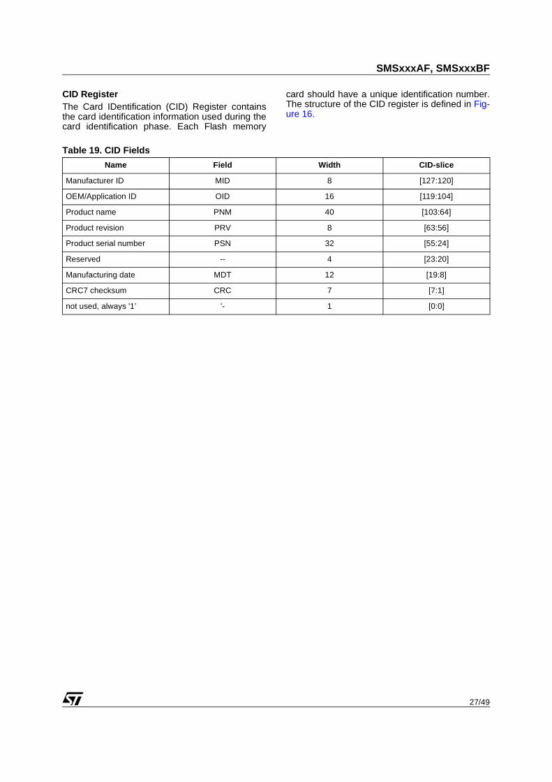
CID RegisterThe Card IDentification (CID) Register containsthe card identification information used during thecard identification phase. Each Flash memory
card should have a unique identification number.The structure of the CID register is defined in Fig-ure 16.
Table 19. CID Fields
Name Field Width CID-slice
Manufacturer ID MID 8 [127:120]
OEM/Application ID OID 16 [119:104]
Product name PNM 40 [103:64]
Product revision PRV 8 [63:56]
Product serial number PSN 32 [55:24]
Reserved -- 4 [23:20]
Manufacturing date MDT 12 [19:8]
CRC7 checksum CRC 7 [7:1]
not used, always '1’ '- 1 [0:0]

SMSxxxAF, SMSxxxBF
28/49
CSD RegisterThe Card Specific Data Register provides informa-tion on how to access the card contents. The CSDRegister defines the data format, error correctiontype, maximum data access time, data transfer
speed, whether the DSR register can be used etc.The programmable register parameters (entrieswith cell type W or R, listed in Table 20.) can bechanged using CMD27.
Table 20. CSD Fields Compatible with CSD Structure V1 / MM Card Specification V2.11
Note: 1. R = readable, W(1) = can be written once, W = can be written several times.
Name Field Width Cell Type(1) CSD-slice
CSD structure CSD_STRUCTURE 2 R [127:126]
reserved - 6 R [125:120]
data read access-time-1 TAAC 8 R [119:112]
data read access-time-2 in CLK cycles (NSAC*100)
NSAC 8 R [111:104]
Max. data transfer rate TRAN_SPEED 8 R [103:96]
card command classes CCC 12 R [95:84]
Max. read data block length READ_BL_LEN 4 R [83:80]
partial blocks for read allowed READ_BL_PARTIAL 1 R [79:79]
write block misalignment WRITE_BLK_MISALIGN 1 R [78:78]
read block misalignment READ_BLK_MISALIGN 1 R [77:77]
DSR implemented DSR_IMP 1 R [76:76]
reserved - 2 R [75:74]
device size C_SIZE 12 R [73:62]
Max. read current @VDD min VDD_R_CURR_MIN 3 R [61:59]
Max. read current @VDD max VDD_R_CURR_MAX 3 R [58:56]
Max. write current @VDD min VDD_W_CURR_MIN 3 R [55:53]
Max. write current @VDD max VDD_W_CURR_MAX 3 R [52:50]
device size multiplier C_SIZE_MULT 3 R [49:47]
erase single block enable ERASE_BLK_EN 1 R [46:46]
sector size SECTOR_SIZE 7 R [45:39]
write protect group size WP_GRP_SIZE 7 R [38:32]
write protect group enable WP_GRP_ENABLE 1 R [31:31]
reserved for MultiMediaCard compatibility - 2 R [30:29]
write speed factor R2W_FACTOR 3 R [28:26]
Max. write data block length WRITE_BL_LEN 4 R [25:22]
partial blocks for write allowed WRITE_BL_PARTIAL 1 R [21:21]
reserved - 5 R [20:16]
File format group FILE_FORMAT_GRP 1 R/W(1) [15:15]
copy flag (OTP) COPY 1 R/W(1) [14:14]
permanent write protection PERM_WRITE_PROTECT 1 R/W(1) [13:13]
temporary write protection TMP_WRITE_PROTECT 1 R/W [12:12]
File format FILE_FORMAT 2 R/W(1) [11:10]
reserved - 2 R/W [9:8]
CRC CRC 7 R/W [7:1]
not used, always'1 '- 1 - [0:0]

29/49
SMSxxxAF, SMSxxxBF
RCA RegisterThe writable 16-bit Relative Card Address Regis-ter contains the card address published by thecard during the identification phase. This addressis used for addressed host-card communicationsafter the card identification phase. The default val-ue of the RCA register is 0000h. This value is re-served, the CMD7 command uses it to set all thecards to the Standby state.DSR Register (Optional)The 16-bit Driver Stage Register is not used in ST-Microelectronics Cards.
SCR RegisterThe SD Card Configuration Register (SCR) is aconfiguration register. The SCR provides informa-tion on the special features that are configured inthe SD Memory Card. The size of SCR Register is64 bit. This register is programmed in the factory by theSD Memory Card manufacturer. Table 21. de-scribes the SCR contents.
Table 21. SCR Fields
Note: 1. R = readable.
Description Field Width Cell Type(1) SCR Slice
SCR Structure SCR_STRUCTURE 4 R [63:60]
SD Memory Card - Specification. Version
SD_SPEC 4 R [59:56]
data_status_after erases DATA_STAT_AFTER_ERASE 1 R [55:55]
SD Security Support SD_SECURITY 3 R [54:52]
DAT Bus width supported SD_BUS_WIDTHS 4 R [51:48]
reserved - 16 R [47:32]
reserved for manufacturer usage - 32 R [31:0]

SMSxxxAF, SMSxxxBF
30/49
TIMINGSThe symbols listed in Table 22. are used in all tim-ing diagrams.The difference between P-bits and Z-bits is that P-bits are actively driven to High by the card or thehost output driver whereas Z-bits are driven toHigh and kept High by the pull-up resistors RCMDand RDAT. P-bits, which are actively driven High,are less sensitive to noise. All timing values aredefined in Table 23.
Table 22. Timing Diagram Symbols
Command and ResponseThe host command and the card response areboth clocked out on the rising edge of the hostclock. Card Identification and Operating ConditionsTimings. The timings for CMD2(ALL_SEND_CID) and ACMD41 are shown in Fig-
ure 17. The command is followed by two Z-bits (toleave time for the bus to switch direction) and thenby P-bits pushed up by the responding card. Thecard response to the host command starts afterNID clock cycles.
Figure 17. Identification Sequence
Card Relative Address Timings. The SD Mem-ory Card timings for CMD3(SEND_RELATIVE_ADDR) are given in Figure
18. The minimum delay between the host com-mand and the card response is NCR clock cycles.
Figure 18. SEND_RELATIVE_ADDRESS Command
Data Transfer Mode. After publishing its RCAthe card switches to the Data Transfer mode. Thecommand is followed by two Z-bits (to leave timetime for the bus to switch direction) and then by P-bits pushed by the responding card as shown in
Figure 19. The timing diagram presented in Figure19. applies to all host commands followed by cardresponses, and to ACMD41 and CMD2 com-mands.
Symbol Description
S Start bit (= ‘0’)
T Transmitter bit (Host = '1', Card = '0')
P One-cycle pull-up (= '1')
E End bit (=1)
Z High impedance state (-> = '1')
D Data bits
X Don't Care data bits (from card)
* Repetition
CRC Cyclic redundancy check bits (7 bits)
Card active
Host active
S T CONTENT CRC E Z Z P *** P S T CONTENT Z Z Z
Host Command CID or OCRNID Cycles
ai10046
CMD
S T CONTENT CRC E Z Z P *** P S T Z Z Z
Host Command ResponseNCR Cycles
ai10047
CONTENT CRC ECMD

31/49
SMSxxxAF, SMSxxxBF
Figure 19. Response (Data Transfer Mode)
Last Card Response, Next Host CommandTimings. After receiving the last card response,the host can start the next command transmission
after NRC clock cycles as shown in Figure 20. Thetiming diagram presented in Figure 20. applies toany host command.
Figure 20. Response End To Next CMD Start (Data Transfer Mode)
Last Host Command, Next Host CommandTimings. The host can send a new commandNCC clock cycles after sending the previous oneas shown in Figure 21.
Figure 21. Command Sequence (All Modes)
S T CONTENT CRC E Z Z P *** P S T Z Z Z
Host Command ResponseNCR Cycles
ai10047
CONTENT CRC ECMD
S T CONTENT CRC E Z ****** Z S T
Response Host CommandNRC Cycles
ai10048
CONTENT CRC ECMD
S T CONTENT CRC E Z ****** Z S T
Host Command Host CommandNCC Cycles
ai10049
CONTENT CRC ECMD

SMSxxxAF, SMSxxxBF
32/49
Data Read Single Block Read. The host selects one cardfor the data read operation by issuing CMD7, andsets the valid block length for oriented data trans-fer by issuing CMD16. Figure 22. shows the tim-ings for a basing bus read operation. Thesequence starts with a Single Block Read com-mand (CMD17) which specifies the start address
in the argument field. The response is sent on theCMD line.Data transmission from the card starts NAC afterthe end bit of the read command, where NAC is theaccess time. CRC check bits are appended to thedata bits to allow the host to check for transmis-sion errors.
Figure 22. Single Block Read Command
Multiple Block Read. In Multiple Block Readmode, the card responds to the read commandfrom the host by sending a continuous flow of datablocks. The data flow is terminated by aSTOP_TRANSMISSION command (CMD12). Fig-ure 23. describes the Multiple Block Read com-
mand followed by the data blocks and Figure 24.,the response to a STOP_TRANSMISSION com-mand. The data transmission stops two clock cy-cles after the end bit of theSTOP_TRANSMISSION command.
Figure 23. Multiple Block Read Command
Figure 24. STOP_TRANSMISSION Command (CMD12, Data Transfer Mode)
S T CONTENT CRC E Z *** P S T
Host Command ResponseNCR Cycles
ai10050
CONTENT CRC ECMD Z P
Z **** ZZ Z Z Z Z Z Z P ********** P S D ***D D
NAC Cycles Read Data
DAT
S T CONTENT CRC E Z * P S T
Host Command ResponseNCR
Cycles
ai10051
CONTENT CRC ECMD Z P
Z **** ZZ Z Z Z Z Z Z P ******* P S D D D
NAC Cycles Read Data
DAT
Z Z P P P P P P P P P
CONTENT CRC E P ******* S D D
P P P P
P
NAC Cycles Read Data
S T CONTENT CRC E Z * * * P S T
Host Command ResponseNCR Cycles
ai10052
CONTENT CRC ECMD Z P
D * * * * * * * * DD D D D E Z Z * * * * * * * * * * * * * * * * * * * *DAT
33/49
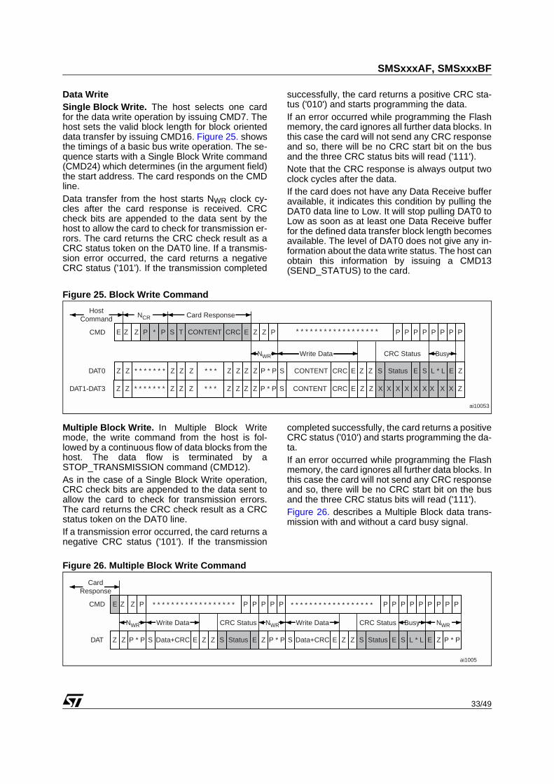
SMSxxxAF, SMSxxxBF
Data WriteSingle Block Write. The host selects one cardfor the data write operation by issuing CMD7. Thehost sets the valid block length for block orienteddata transfer by issuing CMD16. Figure 25. showsthe timings of a basic bus write operation. The se-quence starts with a Single Block Write command(CMD24) which determines (in the argument field)the start address. The card responds on the CMDline. Data transfer from the host starts NWR clock cy-cles after the card response is received. CRCcheck bits are appended to the data sent by thehost to allow the card to check for transmission er-rors. The card returns the CRC check result as aCRC status token on the DAT0 line. If a transmis-sion error occurred, the card returns a negativeCRC status ('101'). If the transmission completed
successfully, the card returns a positive CRC sta-tus ('010') and starts programming the data.If an error occurred while programming the Flashmemory, the card ignores all further data blocks. Inthis case the card will not send any CRC responseand so, there will be no CRC start bit on the busand the three CRC status bits will read ('111'). Note that the CRC response is always output twoclock cycles after the data. If the card does not have any Data Receive bufferavailable, it indicates this condition by pulling theDAT0 data line to Low. It will stop pulling DAT0 toLow as soon as at least one Data Receive bufferfor the defined data transfer block length becomesavailable. The level of DAT0 does not give any in-formation about the data write status. The host canobtain this information by issuing a CMD13(SEND_STATUS) to the card.
Figure 25. Block Write Command
Multiple Block Write. In Multiple Block Writemode, the write command from the host is fol-lowed by a continuous flow of data blocks from thehost. The data flow is terminated by aSTOP_TRANSMISSION command (CMD12).As in the case of a Single Block Write operation,CRC check bits are appended to the data sent toallow the card to check for transmission errors.The card returns the CRC check result as a CRCstatus token on the DAT0 line.If a transmission error occurred, the card returns anegative CRC status ('101'). If the transmission
completed successfully, the card returns a positiveCRC status ('010') and starts programming the da-ta.If an error occurred while programming the Flashmemory, the card ignores all further data blocks. Inthis case the card will not send any CRC responseand so, there will be no CRC start bit on the busand the three CRC status bits will read ('111'). Figure 26. describes a Multiple Block data trans-mission with and without a card busy signal.
Figure 26. Multiple Block Write Command
S
E Z * P S T
HostCommand Card ResponseNCR
ai10053
CONTENT CRC ECMD Z P
Z * * * * * * * ZZ Z Z Z * * * P * P L * L E Z
NWR
DAT0
Z Z P
X X
P P P P
CONTENT CRC E Z E S
P P P P
Status
BusyWrite Data
* * * * * * * * * * * * * * * * * *
Z Z Z Z S
SZ * * * * * * * ZZ Z Z Z * * * P * P X ZDAT1-DAT3 CONTENT CRC E Z X XZ Z Z Z X XX X
CRC Status
E Z
CardResponse
ai1005
CMD Z
NWR
DAT
P P P P P P P P P
Write Data
* * * * * * * * * * * * * * * * * *
CRC Status
P P P P P * * * * * * * * * * * * * * * * * * P
P * P SE ZStatusSSZ P * P Data+CRC E ZZ Z L * L EE SStatusSData+CRC E Z Z Z P * P
NWR Write Data CRC Status NWRBusy

SMSxxxAF, SMSxxxBF
34/49
STOP_TRANSMISSION CommandThe STOP_TRANSMISSION command works inthe same way as in the read mode. Figures 27 to30 describe the timings of theSTOP_TRANSMISSION command in differentcard states.The card will consider that a data block was suc-cessfully received and is ready for programmingonly if the CRC data of the block was validated andthe CRC status token, returned to the host. Figure 28. is an example of an interrupted (by aSTOP_TRANSMISSION command from the host)attempt to transmit the CRC status token. The re-sult is the same as in other examples where theSTOP_TRANSMISSION command is implement-ed: the end bit of the STOP_TRANSMISSIONcommand from the host is followed, on the dataline, by one more data bit, then an end bit and two
Z-bits. The two Z-bits, which correspond to twoclock cycles, are used to switch the bus direction.The received data block is considered incompleteand will not be programmed.In the previous Stop Transmission examples, thehost stopped the data transmission during an ac-tive data transfer. In Figure 29. and Figure 30. theSTOP_TRANSMISSION command is received bythe card after all the data blocks have been sent.In Figure 29., the card is busy programming thelast block when the STOP_TRANSMISSION com-mand is received whereas in Figure 30. the card isidle but the input buffers still contain data blocks tobe programmed. In the second case, the cardstarts programming the blocks upon reception ofthe STOP_TRANSMISSION command and acti-vates the busy signal.
Figure 27. STOP_TRANSMISSION During Data Transfer From The Host
Figure 28. STOP_TRANSMISSION During CRC Status Transfer From Card
Note: 1. The card CRC status response was interrupted by the host.
Figure 29. STOP_TRANSMISSION Received After Last Data Block with Card Busy Programming
ai09518
S T CONTENT CRC E Z * * * * * * P P S T
Host Command Host CommandCard ResponseNCR Cycles
CONTENT S T CONTENTCRC ECMD Z P
D DD D D D D D D D E Z Z LS Z Z Z
Card is programming
DAT E Z Z ZZZ* * * * * * * * * * * * * * * * * * * * * *
ai10062
S T CONTENT CRC E Z P * * * * * * P S T
Host Command HostCommand
Card ResponseNCR Cycles
CONTENT S T CONTENTCRC ECMD Z P
D ZD D D D Z S Status E Z Z LS Z Z Z
Card is programming
DAT E Z Z ZZZ* * * * * * * * * * * * * * * * * * * * * *
DataBlock
CRCStatus(1)
ai10063
S T CONTENT CRC E Z * * * S T
Host Command HostCommand
Card ResponseNCR Cycles
CONTENT S T CONTENTCRC ECMD Z P
LS Z Z Z
Card is programming
DAT E Z Z ZZZ* * * * * * * * * * * * * * * * * * * * * * * * * * * * * * * * * * * * * *
P
L

35/49
SMSxxxAF, SMSxxxBF
Figure 30. STOP_TRANSMISSION Received After Last Data Block with Card Idle
Erase, Set and Clear Write Protect Timings.The host must first tag the start (CMD32) and end(CMD33) addresses of the range to be erased.The Erase command (CMD38), once issued, willerase all the selected write blocks. Similarly, Setand Clear Write Protect commands start a pro-gramming operation as well. The card will signal"busy" (by pulling the DAT line Low) for the dura-tion of the erase or program operation. The bustransaction timings are the same as those givenfor the STOP_TRANSMISSION Command in Fig-ure 30.Re-selecting a busy card. When a busy card inDisabled state is reselected, it restores its busysignaling on the data line. The timing diagram forthis command / response / busy transaction is thesame as that for STOP_TRANSMISSION com-mand illustrated in Figure 30.
Timing ValuesTable 23. gives all timings.
Table 23. Timing Values
ai10064
S T CONTENT CRC E Z * * * S T
Host Command HostCommand
Card ResponseNCR Cycles
CONTENT S T CONTENTCRC ECMD Z P
LS Z Z Z
Card is programming
DAT E Z Z ZZZ* * * * * * * * * * * * * * * * * * * * *
P
LZ Z ZZ Z ZZZ Z Z Z
Parameter Min Max Unit
NCR 2 64 clock cycle
NID 5 5 clock cycle
NAC 2 TAAC + NSAC clock cycle
NRC 8 - clock cycle
NCC 8 - clock cycle
NWR 2 - clock cycle

SMSxxxAF, SMSxxxBF
36/49
SERIAL PERIPHERAL INTERFACE (SPI) MODEThe SPI mode is a secondary communication pro-tocol, which is available in Flash memory-basedSD Memory Cards. The SD Memory Card SPI im-plementation uses a subset of the SD MemoryCard protocol and command set. The advantageof the SPI mode is the capability of using off-the-shelf host, hence reducing the design-in effort to aminimum. The disadvantage is the loss of perfor-mance (e.g., Single data line and hardware CSsignal per card). The SPI mode is selected duringthe first Reset command after power-up (CMD0)and cannot be changed once the part is poweredon.SPI Bus TopologyThe SPI compatible communication mode of theSD Memory Card is designed to communicate withan SPI channel, commonly found in various micro-controllers on the market. The SPI standard de-fines the physical link only, and not the completedata transfer protocol. The SD Memory Card SPIand SD modes use the same command set.
Like all SPI devices, the SD Memory Card SPIchannel uses the four following signals: CS: Host to card Chip Select signal. CLK: Host to card clock signal DataIn: Host to card data signal. DataOut: Card to host data signal.All data tokens are multiples of Bytes (8 bits) andalways Byte-aligned to the CS signal. The cardidentification and addressing methods are re-placed by a hardware Chip Select (CS) signal.There are no broadcast commands. For everycommand, a card (slave) is selected by asserting(active Low) the CS signal (see Figure 31., SDMemory Card System SPI Mode Bus Topolo-gy).The CS signal must be continuously active forthe duration of the SPI transaction. The only ex-ception occurs during card programming, whenthe host can de-assert the CS signal without af-fecting the programming process. The SPI inter-face uses 7 out of the 9 SD signals (DAT1 andDAT2 are not used, DAT3 is the CS signal) of theSD bus.
Figure 31. SD Memory Card System SPI Mode Bus Topology
CS(A)
VDDVSS
CSVDDVSS
CLK, DataIN, DataOut
SD MemoryCard (A)
(SPI mode)
CSVDD
VSS
CLK, DataIN, DataOut
SD MemoryCard (B)
(SPI mode)CLKDataINDataOut
CS
VDD
VSS
CLK, DataIN, DataOut
MultiMediaCard(C)
(SPI mode)
ai10065
HOST
CS(B)
CS(B)

37/49
SMSxxxAF, SMSxxxBF
SPI Bus ProtocolWhereas the SD channel is based on commandand data bit streams initiated by a start bit and ter-minated by a stop bit, the SPI channel is Byte-ori-ented. Every command or data block is built upwith 8-bit Bytes and is Byte-aligned to the CS sig-nal (that is, the length is a multiple of 8 clock cy-cles). Like in the SD protocol, messages in the SPI pro-tocol consist of command, response and data-block tokens. All communications between hostand cards are controlled by the host (master). Thehost starts every bus transaction by asserting theCS signal Low. The response behaviors in SPI mode and SDmode differ in three ways. In the SPI mode: the selected card always responds to the
command. two additional (8 & 16 bit) response structures
are used when the card encounters a data retrieval
problem, it sends an error response in place of the expected data block (in the SD mode the card does not respond but implements a timeout).
In addition to returning a response for every com-mand received, the card returns a special data re-sponse token for every data block received duringwrite operations. Mode Selection. The SD Memory Card wakesup in the SD mode. It will enter the SPI mode if theCS signal is asserted (Low) when the Reset com-mand (CMD0) is received.The only way to return to the SD mode is to start anew power-down/power-up sequence.
In SPI mode, the SD Card protocol state machinedoes not apply.Bus Transfer Protection. On entering the SPImode the card defaults to the non-protected modewhere there is no CRC (Cyclic RedundancyCheck). So systems using reliable data links arenot obliged to have the hardware and firmwarenecessary to implement CRC functions. In non-protected mode, the CRC bits are stillpresent but are Don't Care. The CRC option canbe turned on and off by the host through theCRC_ON_OFF command (CMD59).Data Read. Single and Multiple Block Read oper-ations are supported in SPI mode. The main differ-ence with the SD mode is that in SPI mode dataand responses to the host are both sent on theDataOut line. As a consequence the data transfermay be interrupted and the last data block, re-placed by the response to aSTOP_TRANSMISSION command. The basic unit of data transfer is the block. Themaximum size of a block is defined in the CSDRegister (READ_BL_LEN). If READ_BL_PARTIAL is set, smaller blocks en-tirely contained in a physical block (as defined byREAD_BL_LEN) may also be transmitted. SingleBlock Read operations are initiated by issuing theREAD_SINGLE_BOCK command (CMD17). Thestart address can be any Byte in the valid addressrange of the card. Every block, however, must becontained in a single physical card sector.Multiple Block Read operations are initiated by is-suing the READ_MULTIPLE_BLOCK command(CMD18) and every transferred block has a 16-bitCRC appended to it. The STOP_TRANSMISSIONcommand (CMD12) will actually stop the datatransfer operation (just like in the SD mode).
Figure 32. Read Operation Mechanism
Command CommandData in
Data out
ai10066
from Cardto Host
from Hostto Card
next command
Response Data Block CRC
data from Cardto Host

SMSxxxAF, SMSxxxBF
38/49
Figure 33. Multiple Block Read Operation
Figure 34. Read Data Error
Data Write. Single and Multiple Block Write oper-ations are supported in SPI mode. Upon reception of a valid write command, the cardsends a response token and waits for a data blockto be sent from the host. Write operations, as illus-trated in Figure 35., follow the same rules as Readoperations (refer to Data Write) as regards theCRC, block length and start address.
After receiving a data block, the card returns adata response token. If the data block receivedcontains no error, it is programmed. Throughoutthe programming operation the card sends a con-tinuous stream of busy tokens to the host (by hold-ing the DataOut line Low).
Figure 35. Write Operation
Erase & Write Protect Management. The eraseand write protect management procedures are thesame in the SPI and SD modes.
While the card is erasing or changing the write pro-tection bits, it remains in the busy state and holdsthe DataOut line Low.
Figure 36. Erase & Write Protect Operations
Command STOP_TRANSMISSIONCommand
Data in
Data out
ai10067
from Cardto Host
from Hostto Card
next command
Response Data Block CRC
data from Cardto Host
Data Block CRC Data B. Response
Command CommandData in
Data out
ai10068
from Cardto Host
from Hostto Card
next command
Response Data Error
Data Error messagefrom Card to Host
CommandData in
Data out
ai10069
from Cardto Host
from Hostto Card
Response DataResponse Busy
data fromHost
to Card
Data Block>
DataResponse Busy
Data Block> >
Data starttoken Data Response
and Busyfrom Card
data from Hostto Card Data stop
token
Command CommandData in
Data outai10070
from Cardto Host
from Hostto Card
from Hostto Card
Response Response
from Cardto Host
Busy

39/49
SMSxxxAF, SMSxxxBF
Read CID/CSD Registers. In SPI mode the CIDand CSD Registers use a Block Read operation.When a Read command is issued, the card returnsa response message followed by a 16 Byte datablock with a 16-bit CRC. As TAAC, the Data Read Access Time, is stored inthe CSD Register, it cannot be used as the read la-tency of the CSD Register. NCR (see Table23., Timing Values) is used instead.Reset Sequence. The SD Memory Card requiresa defined reset sequence. After power-on reset orCMD0 (software reset) the card enters an idlestate. When idle, the only host commands the cardwill accept are CMD1 (SEND_OP_COND),ACMD41 (SD_SEND_OP_COND) and CMD58(READ_OCR). In SPI mode CMD1 and ACMD41 have the samefunction. The host must poll the card (by repeated-ly sending CMD1 or ACMD41) until the 'in-idle-state' bit in the card response switches to Low,thus indicating that the card has completed its ini-
tialization process and is ready for the next com-mand. In the SPI mode, as opposed to the SD mode,CMD1 (and ACMD41) has no operands and doesnot return the contents of the OCR register. In-stead, the host may use CMD58 (available in SPImode only) to read the OCR register. Also it is up to the host to pay attention not to gainaccess to cards that do not support its voltagerange. The use of CMD58 is not restricted to theinitializing phase, it can be issued at any time. Memory Array Partitioning. It is the same as inthe SD mode.Card Lock/Unlock Commands. In the SPImode, the Lock and Unlock commands are thesame as in the SD mode.Application Specific Commands. The only dif-ference between the SD and SPI modes is theAPP_CMD status bit, which is not available in theSPI mode.

SMSxxxAF, SMSxxxBF
40/49
SPI Mode CommandsAll the SPI commands are 6 Bytes long. The com-mand always starts with the MSB of the string,which corresponds to the command code. See Ta-ble 24. for details of the command format.Like in the SD mode, the commands in the SPImode are divided into classes. However, theclasses supported by the two modes are different.See Table 25. For details.
The commands supported in the SPI mode are de-scribed in detail in Table 25. If no argument is re-quired in the command, the value of the fieldshould be set to '0'. Reserved commands are re-served in both the MultiMediaCard and SPImodes. The contents of the command index fieldare binary: for example, it is '000000' for CMD0and '100111' for CMD39.For more details about commands and argu-ments, please refer to the SD Memory Card Spec-ification.
Table 24. Command Format
Table 25. Command Classes in SPI Mode
Bit Position 47 46 [45:40] [39:8] [7:1] 0
Width (bits) 1 1 6 32 7 1
Value 0 1 x x x 1
Descriptions start bit transmission bit command index argument CRC7 end bit
Card CMD Class (CCC) Class Description
Supported Commands
0 1 9 10 12 13 16 17 18 24 25 27 28 29 30 32 33 38 42 55 56 58 59
class 0 Basic + + + + + + + +
class 1 Not supported in SPI
class 2 Block Read + + +
class 3 Not supported in SPI
class 4 Block Write + + +
class 5 Erase + + +
class 6 Write Protection (optional)
+ + +
class 7 Lock Card (optional) +
class 8 Application specific + +
class 9 Not supported in SPI
class 10 - class 11
Reserved

41/49
SMSxxxAF, SMSxxxBF
ResponsesThere are several types of response tokens. As inthe SD mode, all are transmitted MSB first.R1 Format. The card sends this response tokenafter every command except for theSEND_STATUS command. R1 Format Responses are one Byte long. TheMSB is always zero and the other bits indicate er-rors, an error being indicated by a '1'. R1b Format. This response token is similar to theR1 Format response token but for the option ofadding the busy signal. The busy signal token can be any number ofBytes. A zero value indicates that the card is busy.A non-zero value indicates that the card is readyfor the next command.R2 Format. This response token is two Byteslong. It is sent as a response to theSEND_STATUS command. R3 Format. This response token is sent by thecard when a READ_OCR command is received.The response length is 5 Bytes. The structure ofthe first Byte is identical to that of the R1 Formatresponse. The other four Bytes contain the OCRregister.For more details about responses, please refer tothe SD Memory Card Specification v.1.01.Clearing Status BitsIn the SPI mode, as described in the previousparagraphs, status bits are reported to the host inthree different formats: R1 Format response, R2Format response and data error token (the samebits may exist in several response types - e.g.Card ECC failed). As in the SD mode, error bits are cleared whenread by the host, regardless of the response for-mat.State indicators are cleared either when read bythe host or in accordance with the card state. Formore details, please refer to the SD Memory CardSpecification.
SPI Bus TimingsFigure 38. illustrates the basic Command/Re-sponse transaction in SPI mode (that is, when thecard is ready).Figure 39. describes a Command/ Responsetransaction when the card is busy (R1b responseformat). For timings, refer to Table 23.
Table 26. SPI Timing Symbols
Table 27. SPI Timing Values
Figure 37. Host Command to Card Response - Card is Ready
S Start Bit (=0)
T Transmitter Bit (Host = 1, Card = 0)
P One-Cycle Pull-up (=1)
E End Bit (= 1)
Z High impedance stage
D Data Bits
* Repeater
Timing Min Max Unit
NCS 0 8 clock cycles
NCR 1 8 8 clock cycles
NCX 0 8 8 clock cycles
NRC 1 8 clock cycles
NAC 1specified in
CSD Register
8 clock cycles
NWR 1 8 clock cycles
NEC 0 8 clock cycles
NDS 0 8 clock cycles
NBR 1 1 8 clock cycles
H L L L * * * * * * * * * * * * * * * * * * * * *CS
X HX H HH H X X XData In
L L L
* * * * * * * * * * H * * H
L H H H
NEC
H
H * * H 6 Byte Command
ai10071
Z HZ H HH H H Z Z1 or 2 Byte ResponseH * * H* * * * * * * * *Data Out Z H H H H
NCS
NEC

SMSxxxAF, SMSxxxBF
42/49
Figure 38. Host Command to Card Response - Card is Busy
Figure 39. Card Response to Host Command
Data Read Timings. The timing diagram for de-selecting the card by de-asserting CS after the lastcard response corresponds to a standard com-mand-to-response timing diagram as illustrated inFigure 39. During open-ended Multiple BlockRead operations, the STOP_TRANSMISSIONcommand may be sent while the card is transmit-
ting data to the host. In this case, the card stopstransmitting the data block within two clock cycles(the bits in the first Byte may not all be set to '1')and returns the response message after a timemeasured in numbers of clock cycles (NCR). SeeFigure 40.., for details. For timings, refer to Table23.
Figure 40. Single Block Read Operation
L L L * * * * * * * * * * * * * * * * * * * * *CS
X H H HH H X XData In
L L L
H * * H
L L H H
NEC
H
H * * H 6 Byte Command
ai10072
Z ZZ H HZ H H ZResponseH * * H* * * * * * * * *Data Out H H H H
NCS
NCR
H H H LL L L L
H H H H X * X H H H * HH
Busy BusyZL
NDS NEC
L L L L * * * * * * * * * * * * * * * * * * * * *CS
H HH HH H X X XData In
L
* * * * * * * * * *
L H H HL
6 Byte Command
ai10073
H HH H HH H Z Z1 or 2 Byte Response H * * H * * * * * * * * *Data Out H H H
NRC
H HH H H HH H
L L L * * * * * * * * * * * * * * * * * * * * *CS
X H
H
HH H X X XData In
H
* * * * * * * * * * * *
H H H HH
Read Command
ai10074
Z HZ H HH Z Z ZCard ResponseH * * H* * * * * * *Data Out H H H
NCR
H X
L L L
H * * H H * H
Data BlockH * * H
NCS NEC
NAC

43/49
SMSxxxAF, SMSxxxBF
Figure 41. STOP_TRANSMISSION between Blocks During Multiple Block Read
Figure 42. STOP_TRANSMISSION within a Block During Multiple Block Read
Figure 43. CSD Register Read Operation
Data Write Timings. The host may deselect acard at any moment during Single and MultipleBlock Write operations. The card will release theDataOut line one clock cycle after it is deselected(CS High). To check whether the card is still busy,the host must reselect it by driving CS Low. Thecard will then take control of the DataOut line oneclock cycle after being reselected. In MultipleBlock Write operations, the timings from the com-
mand being issued to the first data block beingtransmitted by the card are the same as for SingleBlock Write operations (see Figure 44.. for de-tails). The timing of Stop Tran prefixes is the sameas that of data blocks. After the card receives theSTOP_TRANSMISSION command, the data onthe DataOut line is undefined for one Byte (NBR),then a busy message may be sent by the card. Fortimings, refer to Table 23.
L L * * * * * * * * * * * * * * * * * * * * *CS
X HH H HData In
L L L L LH
H * H ReadCommand
ai10075
Z Z CardResponse* * * *Data Out H H H
NCS
NCR
H
H HH H H H H H
H * H
H
H * H
* * * * * * * * * * * STOP_TRAN.CMD
Data Block H * HH * HData Block CardResponse
NAC NAC NCR
L L * * * * * * * * * * * * * * * * * * * * *CS
X HH H HData In
L L L L LH
H * H ReadCommand
ai10076
Z Z CardResponse* * * *Data Out H H H
NCS
NCR
X
H HH H H H H H
H * H
H
H * H
* * * * * * * * STOP_TRAN.CMD
DataH * HData Block CardResponse
NAC NAC NCR
H H HH
HH * *X
L L * * * * * * * * * * * * * * * * * * * * *CS
X X XData In
L H H H HH
H * * H Read Command
ai10077
Z Z Card Response* * * * * *Data Out H H H
NCS
NCR
X XH H H H
Z Z
H * H
ZH * * H
* * * * * * * * * *
Data Block
H
H HH
L L L
H HH * * H
NCX
NEC

SMSxxxAF, SMSxxxBF
44/49
Figure 44. Single Block Write Operation
Figure 45. Multiple Block Write Operation
L L* * * * * * * * * * * * * * * * * * * * *CS
X H HData In
H L L L LH
H * H Write Command
ai10078
Z Z CardResponse* * * *Data Out H H H
NCS
NCR
H HH H H H
H
X * X
H * H Busy
H
Z ZZ
L H H
LDataResponse
NCX
NDS
L L L L LL L
HH H * H H * HH H H HData Block
BusyH H H H H HH
NWR NEC
L* * * * * * * * * * * * * * * * * * * * *CS
H H HData In
L L L L LL
ai10079
H HData
ResponseData Out H H H
NBR
H HH H H H
X * X
H
L L LL L L L LL L
HH H * H H H H HData Block
BusyH H H H H HH
NWR
L L L L
Data Block STOP_TRCMD
H * HH H HH
BusyData
Response Busy H HH H HH
NWR

45/49
SMSxxxAF, SMSxxxBF
PACKAGE MECHANICAL
Figure 46. Full-Size Secure Digital Memory Card Dimensions
Note: Drawing is not to scale.
Table 28. Full-Size Secure Digital Memory Card Mechanical Data
Symbolmillimeters inches
Typ Min Max Typ Min Max
A 2.100 2.050 2.250 0.0827 0.0807 0.0886
D 32.000 31.900 32.100 1.2598 1.2559 1.2638
E 24.000 23.900 24.100 0.9449 0.9409 0.9488
E1 15.000 – – 0.5906 – –
FD 4.000 3.900 4.100 0.1575 0.1535 0.1614
FE 4.000 3.900 4.100 0.1575 0.1535 0.1614
SE 8.125 – – 0.3198 – –
T1 – 1.400 – – 0.0551 –
T9 – 1.400 – – 0.0551 –
T8 – 0.900 – – 0.0353 –
T7 – 1.100 – – 0.04331 –
TD1 – – 1.600 – – 0.06299
TD2 – 5.000 – – 0.19685 –
A
MMC-002
E1 E
TD1
TD2
T7
FE
FD
SE
D
1234567
9
8
T8
T1
T9

SMSxxxAF, SMSxxxBF
46/49
Figure 47. MiniSD Memory Card Dimensions
Package to be announced.
Table 29. MiniSD Memory Card Mechanical DataPackage to be announced.

47/49
SMSxxxAF, SMSxxxBF
PART NUMBERING
Table 30. Ordering Information Scheme
Note: Other digits may be added to the ordering code for preprogrammed parts or other options. Devices are shipped from the factory with the memory content bits erased to ’1’.For further information on any aspect of the device, please contact the nearest ST Sales Office.
Example: SMS 256 A F A 5 E
Memory Card Standard
SMS = Storage Medium, Secure Digital
Density
016 = 16 MBytes
032 = 32 MBytes
064 = 64 MBytes
128 = 128 MBytes
256 = 256 MBytes
512 = 512 MBytes
01G = 1GByte
Options of the Standard
A = SD full size
B = miniSD (reduced size)
Memory Type
F = Flash Memory
Card Version
A
Temperature Range
5 = −25 to 85°C
Packing
E = Lead-Free Package, Standard Packing (tray)
SMSxxxAF, SMSxxxBF
48/49
REVISION HISTORY
Table 31. Document Revision History
Date Rev. Description of Revision
03-Aug-2004 0.1 First issue.

49/49
SMSxxxAF, SMSxxxBF
Information furnished is believed to be accurate and reliable. However, STMicroelectronics assumes no responsibility for the consequences of use of such information nor for any infringement of patents or other rights of third parties which may result from its use. No license is granted by implication or otherwise under any patent or patent rights of STMicroelectronics. Specifications mentioned in this publication are subject to change without notice. This publication supersedes and replaces all information previously supplied. STMicroelectronics products are not
authorized for use as critical components in life support devices or systems without express written approval of STMicroelectronics.
The ST logo is a registered trademark of STMicroelectronics.All other names are the property of their respective owners
© 2004 STMicroelectronics - All rights reserved
STMicroelectronics group of companiesAustralia - Belgium - Brazil - Canada - China - Czech Republic - Finland - France - Germany - Hong Kong - India - Israel - Italy - Japan -
Malaysia - Malta - Morocco - Singapore - Spain - Sweden - Switzerland - United Kingdom - United States of Americawww.st.com