section 5 undersampling applications - … harmonic sampling, bandpass sampling, or super-nyquist...
TRANSCRIPT

1
SECTION 5
UNDERSAMPLING APPLICATIONS
Fundamentals of Undersampling
Increasing ADC SFDR and ENOB using External SHAs
Use of Dither Signals to Increase ADC Dynamic Range
Effect of ADC Linearity and Resolution on SFDR andNoise in Digital Spectral Analysis Applications
Future Trends in Undersampling ADCs
2
SECTION 5
UNDERSAMPLING APPLICATIONSWalt Kester
An exciting new application for wideband, low distortion ADCs is calledundersampling, harmonic sampling, bandpass sampling, or Super-NyquistSampling. To understand these applications, it is necessary to review the basics ofthe sampling process.
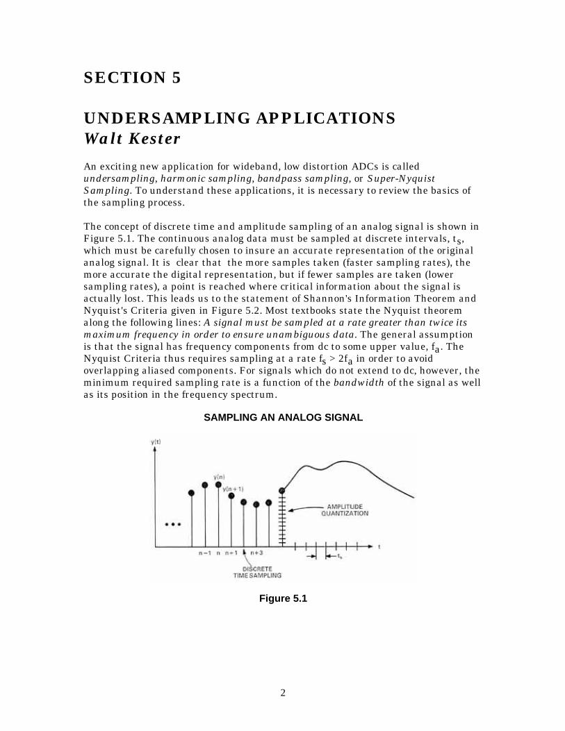
The concept of discrete time and amplitude sampling of an analog signal is shown inFigure 5.1. The continuous analog data must be sampled at discrete intervals, ts,which must be carefully chosen to insure an accurate representation of the originalanalog signal. It is clear that the more samples taken (faster sampling rates), themore accurate the digital representation, but if fewer samples are taken (lowersampling rates), a point is reached where critical information about the signal isactually lost. This leads us to the statement of Shannon's Information Theorem andNyquist's Criteria given in Figure 5.2. Most textbooks state the Nyquist theoremalong the following lines: A signal must be sampled at a rate greater than twice itsmaximum frequency in order to ensure unambiguous data. The general assumptionis that the signal has frequency components from dc to some upper value, fa. TheNyquist Criteria thus requires sampling at a rate fs > 2fa in order to avoidoverlapping aliased components. For signals which do not extend to dc, however, theminimum required sampling rate is a function of the bandwidth of the signal as wellas its position in the frequency spectrum.
SAMPLING AN ANALOG SIGNAL
Figure 5.1

3
SHANNON’S INFORMATION THEOREMAND NYQUIST’S CRITERIA
Shannon:
An Analog Signal with a Bandwidth of fa Must be Sampledat a Rate of fs>2fa in Order to Avoid the Loss ofInformation.The signal bandwidth may extend from DC to fa (BasebandSampling) or from f1 to f2, where fa = f2 - f1 (Undersampling,Bandpass Sampling, Harmonic Sampling, Super-Nyquist)
Nyquist:
If fs<2fa, then a Phenomena Called Aliasing Will Occur.Aliasing is used to advantage in undersamplingapplications.
Figure 5.2
In order to understand the implications of aliasing in both the time and frequencydomain, first consider the four cases of a time domain representation of a sampledsinewave signal shown in Figure 5.3. In Case 1, it is clear that an adequate numberof samples have been taken to preserve the information about the sinewave. In Case2 of the figure, only four samples per cycle are taken; still an adequate number topreserve the information. Case 3 represents the ambiguous limiting condition wherefs=2fa. If the relationship between the sampling points and the sinewave were suchthat the sinewave was being sampled at precisely the zero crossings (rather than atthe peaks, as shown in the illustration), then all information regarding the sinewavewould be lost. Case 4 of Figure 5.3 represents the situation where fs<2fa, and theinformation obtained from the samples indicates a sinewave having a frequencywhich is lower than fs/2, i.e. the out-of -band signal is aliased into the Nyquistbandwidth between dc and fs/2. As the sampling rate is further decreased, and theanalog input frequency fa approaches the sampling frequency fs, the aliased signalapproaches dc in the frequency spectrum.

4
TIME DOMAIN EFFECTS OF ALIASING
Figure 5.3
The corresponding frequency domain representation of the above scenario is shownin Figure 5.4. Note that sampling the analog signal fa at a sampling rate fs actuallyproduces two alias frequency components, one at fs+fa, and the other at fs–fa. Theupper alias, fs+fa, seldom presents a problem, since it lies outside the Nyquistbandwidth. It is the lower alias component, fs–fa, which causes problems when theinput signal exceeds the Nyquist bandwidth, fs/2.

5
FREQUENCY DOMAIN EFFECTS OF ALIASING
Figure 5.4
From Figure 5.4, we make the extremely important observation that regardless ofwhere the analog signal being sampled happens to lie in the frequency spectrum (aslong as it does not lie on multiples of fs/2), the effects of sampling will cause eitherthe actual signal or an aliased component to fall within the Nyquist bandwidthbetween dc and fs/2. Therefore, any signals which fall outside the bandwidth ofinterest, whether they be spurious tones or random noise, must be adequatelyfiltered before sampling. If unfiltered, the sampling process will alias them backwithin the Nyquist bandwidth where they can corrupt the wanted signals.
Methods exist which use aliasing to our advantage in signal processing applications.Figure 5.5 shows four cases where a signal having a 1MHz bandwidth is located indifferent portions of the frequency spectrum. The sampling frequency must bechosen such that there is no overlapping of the aliased components. In general, thesampling frequency must be at least twice the signal bandwidth, and the sampledsignal must not cross an integer multiple of fs/2.

6
MINIMUM SAMPLING RATE REQUIRED FOR NON-OVERLAPPING ALIASING OF A 1MHz BANDWIDTH SIGNAL
Figure 5.5
In the first case, the signal occupies a band from dc to 1MHz, and therefore must besampled at greater than 2MSPS. The second case shows a 1MHz signal whichoccupies the band from 0.5 to 1.5MHz. Notice that this signal must be sampled at aminimum of 3MSPS in order to avoid overlapping aliased components. In the thirdcase, the signal occupies the band from 1 to 2MHz, and the minimum requiredsampling rate for no overlapping aliased components drops back to 2MSPS. The lastcase shows a signal which occupies the band from 1.5 to 2.5MHz. This signal mustbe sampled at a minimum of 2.5MSPS to avoid overlapping aliased components.
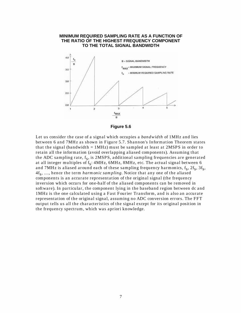
This analysis can be generalized as shown in Figure 5.6. The actual minimumrequired sampling rate is a function of the ratio of the highest frequency component,fMAX, to the total signal bandwidth, B. Notice for large ratios of fMAX to thebandwidth, B, the minimum required sampling frequency approaches 2B.
7
MINIMUM REQUIRED SAMPLING RATE AS A FUNCTION OFTHE RATIO OF THE HIGHEST FREQUENCY COMPONENT
TO THE TOTAL SIGNAL BANDWIDTH
Figure 5.6
Let us consider the case of a signal which occupies a bandwidth of 1MHz and liesbetween 6 and 7MHz as shown in Figure 5.7. Shannon's Information Theorem statesthat the signal (bandwidth = 1MHz) must be sampled at least at 2MSPS in order toretain all the information (avoid overlapping aliased components). Assuming thatthe ADC sampling rate, fs, is 2MSPS, additional sampling frequencies are generatedat all integer multiples of fs: 4MHz, 6MHz, 8MHz, etc. The actual signal between 6and 7MHz is aliased around each of these sampling frequency harmonics, fs, 2fs, 3fs,4fs, ...., hence the term harmonic sampling. Notice that any one of the aliasedcomponents is an accurate representation of the original signal (the frequencyinversion which occurs for one-half of the aliased components can be removed insoftware). In particular, the component lying in the baseband region between dc and1MHz is the one calculated using a Fast Fourier Transform, and is also an accuraterepresentation of the original signal, assuming no ADC conversion errors. The FFToutput tells us all the characteristics of the signal except for its original position inthe frequency spectrum, which was apriori knowledge.

8
INTERMEDIATE FREQUENCY (IF) SIGNAL BETWEEN6 AND 7 MHz IS ALIASED BETWEEN DC AND 1MHz
BY SAMPLING AT 2MSPS
Figure 5.7
A popular application of undersampling is in digital receivers. A simplified blockdiagram of a traditional digital receiver using baseband sampling is shown in Figure5.8. The mixer in the RF section of the receiver mixes the signal from the antennawith the RF frequency of the local oscillator. The desired information is contained inrelatively small bandwidth of frequencies Delta f. In actual receivers, Delta f maybe as high as a few megahertz. The local oscillator frequency is chosen such that theDelta f band is centered about the IF frequency at the bandpass filter output.Popular IF frequencies are generally between 10 and 100MHz. The detector thentranslates the Delta f frequency band down to baseband where it is filtered andprocessed by a baseband ADC. Actual receivers can have several stages of RF and IFprocessing, but the simple diagram serves to illustrate the concepts.
SIMPLIGIED DIGITAL RECEIVERUSING BASEBAND SAMPLING
Figure 5.8
In a receiver which uses direct IF-to-digital techniques (often called undersampling,harmonic, bandpass, or IF sampling), the IF signal is applied directly to a widebandwidth ADC as shown in Figure 5.9. The ADC sampling rate is chosen to be atleast 2 Delta f. The process of sampling the IF frequency at the proper rate causesone of the aliased components of Delta f to appear in the dc to fs/2 Nyquist

9
bandwidth of the ADC output. DSP techniques can now be used to process thedigital baseband signal. This approach eliminates the detector and its associatednoise and distortion. There is also more flexibility in the DSP because the ADCsampling rate can be shifted to tune the exact position of the ∆f signal within thebaseband.
The obvious problem with this approach is that the ADC must now be able toaccurately digitize signals which are well outside the dc to fs/2 Nyquist bandwidthwhich most ADCs were designed to handle. Special techniques are available,however, which can extend the dynamic range of ADCs to include IF frequencies.
SIMPLIFIED DIGITAL RECIEVERUSING IF SAMPLING
Figure 5.9
Let us consider a typical example, where the IF frequency is 72.5MHz, and thedesired signal occupies a bandwidth of 4MHz (B=4MHz), centered on the IFfrequency (see Figure 5.10). We know from the previous discussion that theminimum sampling rate must be greater than 8MHz, probably on the order of10MHz in order to prevent dynamic range limitations due to aliasing. If we place thesampling frequency at the lower band-edge of 70MHz (72.5–2.5), we will definitelyrecover the aliased component of the signal in the dc to 5MHz baseband. There is,however, no need to sample at this high rate, so we may choose any samplingfrequency 10MHz or greater which is an integer sub-multiple of 70MHz, i.e., 70÷2 =35.000MHz, 70÷3 = 23.333MHz, 70÷4 = 17.500MHz, 70÷5 = 14.000MHz, 70÷6 =11.667MHz, or 70÷7 = 10.000MHz. We will therefore choose the lowest possiblesampling rate of 10.000MHz (70÷7).

10
INTERMEDIATE FREQUENCY (IF) SIGNALAT 72.5MHz ( 2MHz) IS ALIASED BETWEENDC AND 5MHz BY SAMPLING AT 10MSPS
Figure 5.10
There is an advantage in choosing a sampling frequency which a sub-multiple of thelower band-edge in that there is no frequency inversion in the baseband alias aswould be the case for a sampling frequency equal to a sub-multiple of the upperband-edge. (Frequency inversion can be easily dealt with in the DSP software shouldit occur, so the issue is not very important).
Undersampling applications such as the one just described generally requiresampling ADCs which have low distortion at the high input IF input frequency. Forinstance, in the example just discussed, the ADC sampling rate requirement is only10MSPS, but low distortion is required (preferably 60 to 80dB SFDR) at the IFfrequency of 72.5MHz.
A large opportunity for bandpass sampling is in digital cellular radio base stations.For systems which have RF frequencies at 900MHz, 70MHz is a popular first-IFfrequency. For systems using an RF frequency of 1.8GHZ, first-IF frequenciesbetween 200 and 240MHz are often used.
In broadband receiver applications, one ADC digitizes multiple channels in thereceive path. Individual channel selection and filtering is done in the digital domain.Narrowband channel characteristics such as bandwidth, passband ripple, andadjacent channel rejection can be controlled with changes to digital parameters (i.e.filter coefficients). Such flexibility is not possible when narrowband analog filters arein the receive path.
Figure 5.11 illustrates the kind of input spectrum an ADC must digitize in amultichannel design. The spectral lines represent narrowband signal inputs from avariety of signal sources at different received power levels. Signal "C" couldrepresent a transmitter located relatively far away from the signal sources "A" and"B". However, the receiver must recover all of the signals with equal clarity. Thisrequires that distortion from the front-end RF and IF signal processing components,

11
including the ADC, not exceed the minimum acceptable level required to demodulatethe weakest signal of interest. Clearly, third-order intermodulation distortiongenerated by "A" and "B" (2B - A, and 2A - B) will distort signals C and D if thenonlinearities in the front-end are severe. Strong out-of-band signals can alsointroduce distortion; signal "E" in Figure 5.11 shows a large signal that is partiallyattenuated by the antialiasing filter. In many systems, the power level of theindividual transmitters is under control of the base station. This capability helps toreduce the total dynamic range required.
BROADBAND DIGITAL RECEIVER ADC INPUT
Figure 5.11
In broadband receiver applications (using an RF frequency of approximately900MHz, and a first-IF frequency of 70MHz), SFDR requirements for the ADC aretypically 70 to 80dBc. Signal bandwidths between 5MHz and 10MHz are common,requiring corresponding sampling rates of 10MSPS to 20MSPS.
Sampling ADCs are generally designed to process signals up to Nyquist (fs/2) with areasonable amount of dynamic performance. As we have seen, however, even thoughthe input bandwidth of a sampling ADC is usually much greater than its maximumsampling rate, the SFDR and effective bit (ENOB) performance usually decreasesdramatically for full scale input signals much above fs/2. This implies that theselection criteria for ADCs used in undersampling applications is SFDR or ENOB atthe IF frequency, rather than sampling rate.
The general procedure for selecting an ADC for an undersampling application is notstraightforward. The signal bandwidth and its location within the frequencyspectrum must be known. The bandwidth of the signal determines the minimumsampling rate required, and in order to ease the requirement on the antialiasingfilter, a sampling rate of 2.5 times the signal bandwidth works well. Afterdetermining the approximate sampling frequency needed, select the ADC based onthe required SFDR, S/(N+D), or ENOB at the IF frequency. This is where thedilemma usually occurs. You will find that an ADC specified for a maximumsampling rate of 10MSPS, for instance, will not have adequate SFDR at the IFfrequency (72.5MHz in the example above), even though its performance is excellentup to its Nyquist frequency of 5Mhz. In order to meet the SFDR, S/(N+D), or ENOB

12
requirement, you will generally require an ADC having a much higher sampling ratethan is actually needed.
Figure 5.12 shows the approximate SFDR versus input frequency for theAD9022/AD9023 (20MSPS), AD9026/AD9027 (31MSPS), and the AD9042 (40MSPS)series of low distortion ADCs. Notice that the AD9042 has superior SFDRperformance.
SFDR COMPARISON BETWEEN 12-BIT SAMPLING ADCs
Figure 5.12
The AD9042 is a state-of-the-art 12-bit, 40MSPS two stage subranging ADCconsisting of a 6-bit coarse ADC and a 7-bit residue ADC with one bit of overlap tocorrect for any DNL, INL, gain or offset errors of the coarse ADC, and offset errorsin the residue path. A block diagram is shown in Figure 5.13. A proprietary gray-code architecture is used to implement the two internal ADCs. The gain alignmentsof the coarse and residue, likewise the subtraction DAC, rely on the statisticalmatching of the process. As a result, 12-bit integral and differential linearity isobtained without laser trim. The internal DAC consists of 126 interdigitated currentsources. Also on the DAC reference are an additional 20 interdigitated currentsources to set the coarse gain, residue gain, and full scale gain. The interdigitizationremoves the requirement for laser trim. The AD9042 is fabricated on a high speeddielectrically isolated complementary bipolar process. The total power dissipation isonly 575mW when operating on a single +5V supply.

13
BLOCK DIAGRAM OF AD9042 12-BIT, 40MSPS ADC
Figure 5.13
AD9042 12-BIT, 40MSPS ADC KEY SPECIFICATIONS
Input Range: 1V peak-to-peak, Vcm = +2.4V
Input Impedance: 250 to Vcm
Effective Input Noise: 0.33LSBs rms
SFDR at 20MHz Input: 80dB
S/(N+D) at 20MHz Input = 66dB
Digital Outputs: TTL Compatible
Power Supply: Single +5V
Power Dissipation: 575mW
Fabricated on High Speed Dielectrically Isolated ComplementaryBipolar Process
Figure 5.14
The outstanding performance of the AD9042 is partly due to the use of differentialtechniques throughout the device. The low distortion input amplifier converts thesingle-ended input signal into a differential one. If maximum SFDR performance isdesired, the signal source should be coupled directly into the input of the AD9042without using a buffer amplifier. Figure 5.15 shows a method using capacitivecoupling.

14
INPUT STRUCTURE OF AD9042 ADC ISDESIGNED TO BE DRIVEN DIRECTLY FROM 50
SOURCE FOR BEST SFDR
Figure 5.15
INCREASING ADC SFDR AND ENOB USING EXTERNALSHAS
An external SHA can increase the SFDR and ENOB of a sampling ADC forundersampling applications if properly selected and interfaced to the ADC. The SHAmust have low hold-mode distortion at the frequency of interest. In addition, theacquisition time must be short enough to operate at the required samplingfrequency. Figure 5.17 shows the effects of adding a SHA to an 8-bit flash converter.The ADC is clocked at 20MSPS, and the input frequency to the ADC is 19.98MHz.The scope photo shows the "beat" frequency of 2kHz reconstructed with an 8-bitDAC. Notice that without the SHA, the ADC has non-linearities and missing codes.The addition of the SHA (properly selected and timed) greatly improves the linearityand reduces the distortion.

15
THE ADDITION OF AN EXTERNAL WIDEBAND LOWDISTORTIOIN SHA EXTENDS THE LOW FREQUENCY
PERFORMANCE OF THE ADC TO HIGHER FREQUENCIES
Figure 5.16
EFFECTS OF EXTERNAL SHA ON FLASH ADCPERFORMANCE FOR fin = 19.98MHz, fs = 20.00MSPS
Figure 5.17

16
Most SHAs are specified for distortion when operating in the track mode. What is ofreal interest, however, is the signal distortion in the hold mode when the SHA isoperating dynamically. The AD9100 (30MSPS) and AD9101(125MSPS) are ultra-fast SHAs and are specified in terms of hold-mode distortion. The measurement isdone using a high performance low distortion ADC (such as the AD9014 14-bit,10MSPS) to digitize the held value of the SHA output. An FFT is performed on theADC output, and the distortion is measured digitally. For sampling rates greaterthan 10MSPS, the ADC is clocked at an integer sub-multiple of the SHA samplingfrequency. This causes a frequency translation in the FFT output because ofundersampling, but the distortion measurement still represents that of the SHAwhich is operating at the higher sampling rate. The AD9100 is optimized for lowdistortion up to 30MSPS, while the AD9101 will provide low distortion performanceup to a sampling rate of 125MSPS. The low distortion performance of these SHAs isprimarily due to the architecture which differs from the classical open-loop SHAarchitecture shown in Figure 5.18.
CLASSIC OPEN-LOOP SHA ARCHITECTURE
Figure 5.18
The sampling switch in the classic open-loop architecture is not within a feedbackloop, and therefore distortion is subject to the non-linearity of the switch. TheAD9100/AD9101 architecture shown in Figure 5.19 utilizes switches inside thefeedback loop to achieve better than 12-bit AC and DC performance. The devices arefabricated on a high speed complementary bipolar process. In the track mode, S1applies the buffered input signal to the hold capacitor, CH, and S2 provides negativefeedback to the input buffer. In the hold mode, both switches are disconnected fromthe hold capacitor, and negative feedback to the input buffer is supplied by S1. Thisarchitecture provides extremely low hold-mode distortion by maintaining high loopgains at high frequency. The output buffer can be configured to provide voltage gain(AD9101), which allows the switches to operate on lower common-mode voltage,thereby giving lower overall distortion.

17
CLOSED-LOOP SHA ARCHITECTUREPROVIDES LOW DISTORTION AND HIGH SPEED
(AD9100, AD9101)
Figure 5.19
The hold-mode SFDR of the AD9100 is a function of the peak-to-peak input signallevel and frequency as shown in Figure 5.20. Notice the data was taken as asampling frequency of 10MSPS for three input amplitudes. The test configuration ofFigure 5.21 was used to collect the data. For each input amplitude, the gain of the opamp between the AD9100 and the AD9014 ADC was adjusted such that the signalinto the AD9014 was always full scale (2V peak-to-peak). Notice that optimumSFDR was obtained with a 200mV p-p input signal. Timing between the SHA andthe ADC is critical. The SHA acquisition time should be long enough to achieve thedesired accuracy, but short enough to allow sufficient hold-time for the ADC front-end to settle and yield a low-distortion conversion. For the test configuration shown,the optimum performance was achieved using an acquisition time of 20ns and a holdtime of 80ns. The ADC is clocked close to the end of the SHA's hold time. Bestperformance in this type of application is always achieved by optimizing the timingin the actual circuit.

18
AD9100 HOLD-MODE SFDR MEASURED ATA SAMPLING RATE OF 10MSPS
Figure 5.20
TEST CONFIGURATION AND TIMING FORMEASURING AD9100 SFDR AT 10MSPS
Figure 5.21
Figure 5.22 shows the SFDR of the AD9100 superimposed on the SFDR of theAD9026/AD9027 and the AD9042 ADCs. These data indicate that the AD9100 willsignificantly improve the SFDR of the AD9026/AD9027 ADC at the higher inputfrequencies. The performance of the AD9042 indicates that SFDR improvements willonly occur at input frequencies above 40MHz.

19
SFDR PERFORMANCE OF AD9100 SHA,AD9026/AD9027 ADC, AND AD9042 ADC
Figure 5.22
The performance of the AD9100 SHA driving the AD9026/AD9027 ADC at asampling frequency of 10MSPS is shown in Figure 5.23. The input signal is a 200mVpeak-to-peak 71.4MHz sinewave. The amplifier between the SHA and the ADC isadjusted for a gain of 10. The SFDR is 72dBc, and the SNR is 62dB.
FFT OUTPUT FOR AD9100 SHA DRIVING AD9026 ADC:INPUT = 200mV p-p, G = 10, fs = 10MSPS, fin = 71.4MHz
Figure 5.23
Similar dynamic range improvements can be achieved with high speed flashconverters at higher sampling rates with the AD9101 SHA. The architecture is

20
similar to the AD9100, but the output buffer amplifier is optimized for a gain of 4(see Figure 5.24). This configuration allows the front end sampler to operate atrelatively low signal amplitudes, resulting in dramatic improvement in hold-modedistortion at high input frequencies and sampling rates up to 125MSPS. TheAD9101 has an input bandwidth of 350MHz and an acquisition time of 7ns to 0.1%and 11ns to 0.01%.
AD9101 125MSPS SHA
Figure 5.24
A block diagram and a timing diagram is shown for the AD9101 driving the AD90028 bit flash converter at 125MSPS (Figure 5.25). The corresponding dynamic rangewith and without the AD9101 is shown in Figure 5.26.

21
AD9101 SHA DRIVING AD9002 8-BIT, 125MSPSFLASH CONVERTER FOR IMPROVED DYNAMIC RANGE
Figure 5.25
AD9002 DYNAMIC PERFORMANCEWITH AND WITHOUT AD9101 SHA
Figure 5.26

22
USE OF DITHER SIGNALS TO INCREASE ADC DYNAMICRANGE
In the development of classical ADC quantization noise theory, the assumption isusually made that the quantization error signal is uncorrelated with the ADC inputsignal. If this is true, then the quantization noise appears as random noise spreaduniformly over the Nyquist bandwidth, dc to fs/2, and it has an rms value equal toq/(sqrt 12). If, however, the input signal is locked to an non-prime integer sub-multiple of fs, the quantization noise will no longer appear as uniformly distributedrandom noise, but instead will appear as harmonics of the fundamental inputsinewave. This is especially true if the input is an exact even submultiple of fs.Figure 5.27 illustrates the point using FFT simulation for an ideal 12 bit ADC. TheFFT record length was chosen to be 4096. The spectrum on the left shows the FFToutput when the input signal is an exact even submultiple (1/32) of the samplingfrequency (the frequency was chosen so that there were exactly 128 cycles perrecord). The SFDR is approximately 78dBc. The spectrum on the right shows theoutput when the input signal is such that there are exactly 127 cycles per record.The SFDR is now about 92dBc which is an improvement of 14dB. Signal-correlatedquantization noise is highly undesirable in spectral analysis applications, where itbecomes difficult to differentiate between real signals and system-induced spuriouscomponents, especially when searching the spectrum for the presence of low-levelsignals in the presence of large signals.
EFFECTS OF SAMPLING A SIGNAL WHICH IS AN EXACT EVENSUB-MULTIPLE OF THE ADC SAMPLING FREQUENCY
(M = 4096, IDEAL 12-BIT ADC SIMULATION)
Figure 5.27
There are a number of ways to reduce this effect, but the easiest way is to add asmall amount of broadband rms noise to the ADC input signal as shown in Figure5.28. The rms value of this noise should be equal to about 1/2 LSB. The effect of thisis to randomize the quantization noise and eliminate its possible signal-dependence.In most systems, there is usually enough random noise present on the input signalso that this happens automatically. This is especially likely when using high speedADCs which have 12 or more bits of resolution and a relatively small input range of2V p-p or less. The total noise at the ADC is composed of the noise of the inputsignal, the effective input noise of the ADC, and an additional component caused by

23
the effects of the sampling clock jitter. In most cases, the rms value of the total ADCinput noise is greater than 1/2 LSB.
THE ADDITION OF WIDEBAND GAUSSIAN NOISETO THE ADC INPUT RANDOMIZES QUANTIZATION
NOISE AND REMOVES INPUT SIGNAL DEPENDENCE
Figure 5.28
EFFECT OF ADC LINEARITY AND RESOLUTION ON SFDRAND NOISE IN DIGITAL SPECTRAL ANALYSISAPPLICATIONS
In order to understand the relationships between ADC resolution, noise, andSpurious Free Dynamic Range (SFDR), it is first necessary to review the some of theissues relating to digital spectral analysis, specifically the FFT. The FFT takes adiscrete number of time samples, M, and converts them into M/2 discrete spectralcomponents. The spacing between the spectral lines is Delta f = fs/M. When a fullscale sinewave signal is applied to an ADC having a resolution of N bits, thetheoretical rms signal to rms noise ratio is 6.02N + 1.76dB. If the quantization noiseis uncorrelated with the signal, it appears as gaussian noise spread uniformly overthe bandwidth dc to fs/2. The FFT acts as a narrowband filter with a bandwidth ofDelta f, and the FFT noise floor is therefore 10log10(M/2) dB below the broadbandquantization noise level (6.02N + 1.76dB). The FFT noise floor is pushed down by3dB each time the FFT record length, M, is doubled (see Figure 5.29). This reductionin the noise floor is the same effect achieved by narrowing the bandwidth of ananalog spectrum analyzer to a bandwidth of fs/M.
For example, a 4096 point FFT has a noise floor which is 33dB below the theoreticalbroadband rms quantization noise floor of 74dB for a 12-bit ADC as shown in Figure5.30 (where the average noise floor is about 74 + 33 = 107dB below full scale). Noticethat there are random peaks and valleys around the average FFT noise floor. These

24
peaks (due to quantization noise, FFT artifacts, and roundoff error) limit the idealSFDR to about 92dBc.
RELATIONSHIP BETWEEN AVERAGE NOISE IN FFT BINSAND BROADBAND RMS QUANTIZATION NOISE LEVEL
Figure 5.29

25
NOISE FLOOR FOR AN IDEAL 12-BIT ADCUSING 4096-POINT FFT
Figure 5.30
Approximately the same dynamic range could be achieved by reducing the resolutionof the ADC to 11 bits and using a 16,384 point FFT. There is a tradeoff, however,because lower resolution ADCs tend to have quantization noise which is correlatedto the input signal, thereby producing larger frequency spurs. Averaging the resultsof several FFTs will tend to smooth out the FFT noise floor, but does nothing toreduce the average noise floor.
Using more bits improves the SFDR only if the ADC AC linearity improves with theadditional bits. For instance, there would be little advantage in using a 14-bit ADCwhich has only 12-bit linearity. The extra bits would only serve to slightly reduce theoverall noise floor, but the improvement in SFDR would be only marginal.
FUTURE TRENDS IN UNDERSAMPLING ADCS
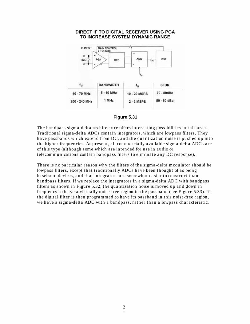
Future ADCs specifically designed for undersampling applications will incorporatethe previously discussed techniques in a single-chip designs. These ADCs will becharacterized by their wide SFDR at input frequencies extending well above theNyquist limit, fs/2. The basic architecture of the digital IF receiver is shown inFigure 5.31. The addition of a low-distortion PGA under DSP control increases thedynamic range of the system. IF frequencies associated with 900MHz digital cellularbase stations are typically around 70MHz with bandwidths between 5 and 10MHz.SFDR requirements are between 70 and 80dBc. On the other hand, 1.8GHZ digitalreceivers typically have IF frequencies between 200 and 240MHz with bandwidths of1MHz. SFDR requirements are typically 50dBc.
26
DIRECT IF TO DIGITAL RECEIVER USING PGATO INCREASE SYSTEM DYNAMIC RANGE
Figure 5.31
The bandpass sigma-delta architecture offers interesting possibilities in this area.Traditional sigma-delta ADCs contain integrators, which are lowpass filters. Theyhave passbands which extend from DC, and the quantization noise is pushed up intothe higher frequencies. At present, all commercially available sigma-delta ADCs areof this type (although some which are intended for use in audio ortelecommunications contain bandpass filters to eliminate any DC response).
There is no particular reason why the filters of the sigma-delta modulator should belowpass filters, except that traditionally ADCs have been thought of as beingbaseband devices, and that integrators are somewhat easier to construct thanbandpass filters. If we replace the integrators in a sigma-delta ADC with bandpassfilters as shown in Figure 5.32, the quantization noise is moved up and down infrequency to leave a virtually noise-free region in the passband (see Figure 5.33). Ifthe digital filter is then programmed to have its passband in this noise-free region,we have a sigma-delta ADC with a bandpass, rather than a lowpass characteristic.

27
REPLACING INTEGRATORS WITH BANDPASSFILTERS GIVES A BANDPASS SIGMA-DELTA ADC
Figure 5.32
NOISE SHAPING FUNCTIONS FOR TRADITIONAL ANDBANDPASS SIGMA-DELTA ADCs
Figure 5.33
The theory is straightforward, but the development of a sigma-delta ADC isexpensive, and there is no universal agreement on ideal characteristics for such abandpass sigma-delta ADC, so developing such a converter from scratch to verify thetheory would be unlikely to yield a commercial product. Researchers at AnalogDevices and the University of Toronto (See References 16, 17, and 18) have thereforemodified a commercial baseband (audio) sigma-delta ADC chip by rewiring itsintegrators as switched capacitor bandpass filters and reprogramming its digital

28
filter and decimator. This has provided a fast, and comparatively inexpensive, proofof the concept, but at the expense of relative low Effective Bits (11-bits), the result ofless than ideal bandpass filters. Nevertheless the results are extremely encouragingand open the way to the design of purpose-built bandpass sigma-delta ADC chips forspecific ASIC applications, especially, but not exclusively, radio receivers.
The overall performance characteristics of the experimental ADC are shown inFigure 5.34. The device was designed to digitize the popular radio IF frequency of455kHz.
SUMMARY OF RESULTS FOR EXPERIMENTALBANDPASS SIGMA-DELTA ADC
Center Frequency: 455kHz
Bandwidth: 10kHz
Sampling Rate: 1.852MSPS
Oversampling Ratio: 91
SNR in Specified Band: 65dB
Supply: 5V, Power: 750mW
Process: 3 m CMOS, Active Area: 1.8 x 3.4 mm
Figure 5.34
In the future it may be possible to have such bandpass sigma-delta ADCs with user-programmable digital filter coefficients, so that the passband of a receiver could bemodified during operation in response to the characteristics of the signal (and theinterference!) being received. Such a function is very attractive, but difficult toimplement, since it would involve loading, and storing, several hundreds or eventhousands of 16-22 bit filter coefficients, and would considerably increase the size,and cost, of the converter.
A feature which could be added comparatively easily to a sigma-delta ADC is a morecomplex digital filter with separate reference (I) and quadrature (Q) outputs. Such afeature would be most valuable in many types of radio receivers.
Technology exists today which should allow the bandpass sigma-delta architectureto achieve 16-bit resolution, SFDR of 70 to 80dBc, and an effective throughput rateof 10 to 20MSPS (input sampling rate = 100MSPS, corresponding to anoversampling ratio of 5 to 10). This would allow 40MHz IF with a 2MHz bandwidthto be digitized directly.

29
CHARACTERISTICS OF A BANDPASS SIGMA-DELTAADC DESIGN FOR IF-SAMPLING
IF Frequency: 40 to 70MHz
Signal Bandwidth: 2MHz
Input Sampling Rate: 100MSPS
Output Data Rate: 10 to 20MSPS
Process: BiCMOS
Figure 5.35
EFFECTS OF SAMPLING CLOCK JITTER INUNDERSAMPLING APPLICATIONS
The effects of sampling clock jitter on Signal-to-Noise Ratio (SNR) and Effective Bit(ENOB) performance discussed in Section 3 are even more dramatic inundersampling applications because of the higher input signal frequencies. Figure5.36 shows the relationship between sampling clock jitter and SNR previouslypresented.
Consider the case where the IF frequency is 70MHz, and 12-bit dynamic range isrequired (70 to 80dB). From Figure 5.36, the rms sampling clock jitter required tomaintain this SNR is approximately 1ps rms. This assumes an ideal ADC with nointernal aperture jitter. ADC aperture jitter combines with the sampling clock jitterin an rms manner to further degrade the SNR.
SNR DUE TO SAMPLING CLOCK JITTER (tj)
Figure 5.36

30
The implications of this analysis are extremely important in undersamplingapplications. The ADC aperture jitter must be minimal, and the sampling clockgenerated from a low phase-noise quartz crystal oscillator. Furthermore, theoscillator should use discrete bipolar and FET devices in the circuits recommendedby the crystal manufacturers. The popular oscillator design which uses a resistor,one or more logic gates, a quartz crystal, and a couple of capacitors should never beused! For very high frequency clocks, a surface acoustic wave (SAW) oscillator ispreferable.
SAMPLING CLOCK OSCILLATORS
Figure 5.37
The sampling clock should be isolated as much as possible from the noise present inthe digital parts of the system. There should be few or no logic gates in the samplingclock path, as a single ECL gate has approximately 4ps rms timing jitter. Thesampling clock generation circuitry should be on separate chips, perhaps withseparately decoupled power supplies, from the remainder of the digital system, andthe sampling clock signal lines should not be located where they can pick up digitalnoise from the rest of the system. All sampling clock circuitry should be groundedand decoupled to the analog ground plane, as would be the case for a critical analogcomponent.
Of course, the sampling clock is itself a digital signal. It has as much potential forcausing noise in the analog part of the system as any other digital signal. Wetherefore see that a sampling clock is very inconvenient, as it must be isolated fromboth the analog and digital parts of the system.
Because the sampling clock jitter is wideband and therefore creates widebandrandom noise, digital filtering can be used to reduce its effects in a system. In thecase of an FFT, however, doubling the FFT record length reduces the noise floor byonly 3dB.
This discussion illustrates the basic fact that undersampling systems havefundamental limitations with respect to their ability to process wide dynamic rangebroadband signals, and system tradeoffs between broadband and narrowbandapproaches must ultimately be made in the design of such systems.
31
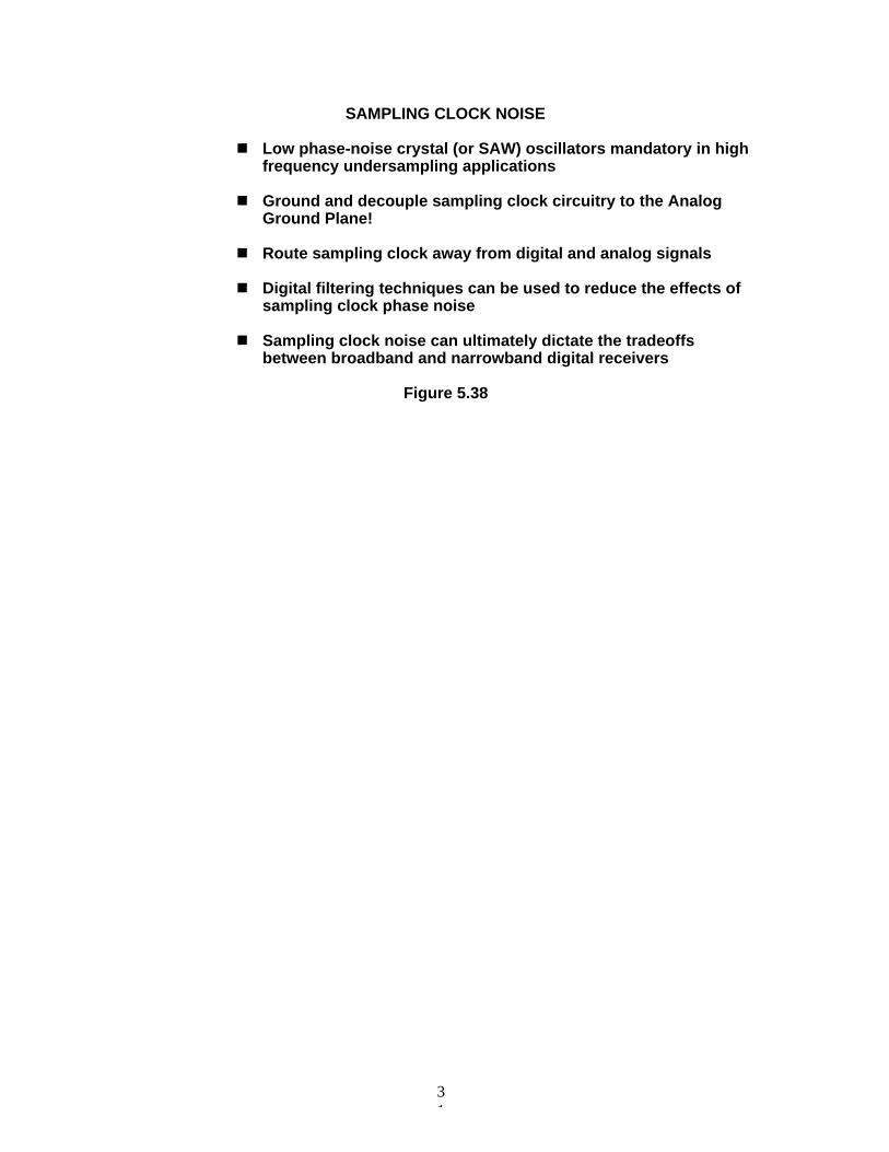
SAMPLING CLOCK NOISE
Low phase-noise crystal (or SAW) oscillators mandatory in highfrequency undersampling applications
Ground and decouple sampling clock circuitry to the AnalogGround Plane!
Route sampling clock away from digital and analog signals
Digital filtering techniques can be used to reduce the effects ofsampling clock phase noise
Sampling clock noise can ultimately dictate the tradeoffsbetween broadband and narrowband digital receivers
Figure 5.38

32
REFERENCES
1. System Applications Guide, Analog Devices, 1993, Chapter 15.
2. Richard Groshong and Stephen Ruscak, Undersampling TechniquesSimplify Digital Radio, Electronic Design, May 23, 1991, pp. 67-78.
3. Richard Groshong and Stephen Ruscak, Exploit Digital AdvantagesIn An SSB Receiver, Electronic Design, June 13, 1991, pp. 89-96.
4. Richard G. Lyons, How Fast Must You Sample?, Test and MeasurementWorld, November, 1988, pp. 47-57.
5. Richard C. Webb, IF Signal Sampling Improves Receiver DetectionAccuracy, Microwaves and RF, March, 1989, pp. 99-103.
6. Jeff Kirsten and Tarlton Fleming, Undersampling ReducesData-Acquisition Costs For Select Applications, EDN, June 21, 1990,pp 217-228.
7. Hans Steyskal and John F. Rose, Digital Beamforming For RadarSystems, Microwave Journal, January, 1989, pp. 121-136.
8. Tom Gratzek and Frank Murden, Optimize ADCs For EnhancedSignal Processing, Microwaves and RF, Vol. 30, No.3, March, 1991,pp. 129-136.
9. Howard Hilton, 10-MHz ADC With 110dB Linearity, High Speed ADCConference, Las Vegas, April 21-22, 1992.
10. Howard Hilton, 10MSample/Second ADC With Filter And Memory, HighSpeed ADC Conference, Las Vegas, April 21-22, l992.
11. Dan Asta, Recent Dynamic Range Characterization of Analog-to-DigitalConverters for Spectral Analysis Applications, Project Report AST-14,MIT Lincoln Laboratory, Lexington, MA, July 9, 1991.
12. Fred H. Irons and T.A. Rebold, Characterization of High-FrequencyAnalog-to-Digital Converters for Spectral Analysis Applications, ProjectReport AST-2, MIT Lincoln Laboratory, November 28, 1986.
13. F. H. Irons, Dynamic Characterization and Compensation of Analog-to-Digital Converters, IEEE International Symposium on Circuits andSystems, May 1986, San Jose, CA. Catalog No. CH2255-8/86/0000-1273.
14. T.A. Rebold and F. H. Irons, A Phase-Plane Approach to the Compensationof High-Speed Analog-to-Digital Converters, IEEE InternationalSymposium on Circuits and Systems, Philadelphia, PA, May, 1987.

33
15. Dan Asta and Fred H. Irons, Dynamic Error Compensation of Analog-to-Digital Converters, The Lincoln Laboratory Journal, Vol. 2, No. 2, 1989,pp. 161-182.
16. James M. Bryant, Bandpass Sigma-Delta ADCs for Direct IF Conversion,DSP- The Enabling Technology for Communications, RAICongrescentrum, Amsterdam, Netherlands, 9-10 March 1993.
17. S.A. Jantzi, M. Snelgrove, P.F. Ferguson, Jr., A 4th-Order BandpassSigma-Delta Modulator, Proceedings of the IEEE 1992 CustomIntegrated Circuits Conference, pp. 16.5.1-4.
18. S.A. Jantzi, R. Schreier, and M. Snelgrove, A Bandpass Sigma-DeltaConvertor for a Digital AM Receiver, Proceedings of the IEEInternational Conference on Analogue-to-Digital and Digital-to-Analogue Conversion, Swansea, UK., September, 1991, pp. 75-80.
19. S.A. Jantzi, W. Martin Snelgrove, and Paul F. Ferguson, Jr., A Fourth-Order Bandpass Sigma-Delta Modulator, IEEE Journal of Solid-StateCircuits, Vol. 38, No. 3, March 1993, pp. 282-291.
20. Barrie Gilbert, A Low Noise Wideband Variable-Gain Amplifier Usingan Interpolated Ladder Attenuator, IEEE ISSCC Technical Digest,1991, pages 280, 281, 330.
21. Barrie Gilbert, A Monolithic Microsystem for Analog Synthesis of Trigonometric Functions and their Inverses, IEEE Journal of SolidState Circuits, Vol. SC-17, No. 6, December 1982, pp. 1179-1191.
22. 1992 Amplifier Applications Guide, Analog Devices, Norwood MA,1992.
23. Carl Moreland, An 8-Bit 150MSPS Serial ADC, 1995 ISSCC Digest ofTechnical Papers, Vol. 38, pp. 272.
24. Roy Gosser and Frank Murden, A 12-Bit 50MSPS Two-Stage A/DConverter, 1995 ISSCC Digest of Technical Papers, p. 278.