section 12. i/o ports - microchip...
TRANSCRIPT
Section 12. I/O Ports
I/O P
orts
12
HIGHLIGHTSThis section of the manual contains the following topics:
12.1 Introduction.............................................................................................................. 12-2
12.2 Control Registers ..................................................................................................... 12-3
12.3 Modes of Operation ................................................................................................. 12-8
12.4 Operation in Power-Saving Modes........................................................................ 12-17
12.5 Effects of Various Resets....................................................................................... 12-17
12.6 Related Application Notes ..................................................................................... 12-18
12.7 Revision History..................................................................................................... 12-19
© 2007-2015 Microchip Technology Inc. DS60001120F-page 12-1
PIC32 Family Reference Manual
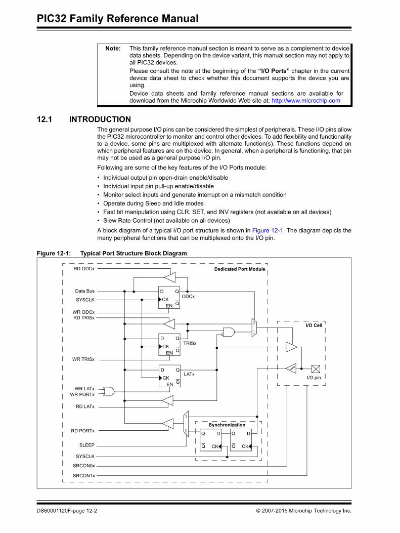
12.1 INTRODUCTIONThe general purpose I/O pins can be considered the simplest of peripherals. These I/O pins allow the PIC32 microcontroller to monitor and control other devices. To add flexibility and functionality to a device, some pins are multiplexed with alternate function(s). These functions depend on which peripheral features are on the device. In general, when a peripheral is functioning, that pin may not be used as a general purpose I/O pin.
Following are some of the key features of the I/O Ports module:
• Individual output pin open-drain enable/disable
• Individual input pin pull-up enable/disable
• Monitor select inputs and generate interrupt on a mismatch condition
• Operate during Sleep and Idle modes
• Fast bit manipulation using CLR, SET, and INV registers (not available on all devices)
• Slew Rate Control (not available on all devices)
A block diagram of a typical I/O port structure is shown in Figure 12-1. The diagram depicts the many peripheral functions that can be multiplexed onto the I/O pin.
Figure 12-1: Typical Port Structure Block Diagram
Note: This family reference manual section is meant to serve as a complement to device data sheets. Depending on the device variant, this manual section may not apply to all PIC32 devices. Please consult the note at the beginning of the “I/O Ports” chapter in the current device data sheet to check whether this document supports the device you are using. Device data sheets and family reference manual sections are available for download from the Microchip Worldwide Web site at: http://www.microchip.com
WR LATx
I/O pin
WR PORTx
Data Bus
RD LATx
RD PORTx
RD TRISx
WR TRISx
I/O Cell
Dedicated Port Module
0
1
RD ODCx
SYSCLK
QD
CKEN Q
QD
CKEN Q
QD
CKEN Q
Q D
CKQ
Q D
CKQ
0
1
Synchronization
SYSCLK
WR ODCx
ODCx
TRISx
LATx
SLEEP
SRCON1x
SRCON0x
DS60001120F-page 12-2 © 2007-2015 Microchip Technology Inc.
Section 12. I/O PortsI/O
Po
rts
12
12.2 CONTROL REGISTERS
Before reading and writing any I/O port, the desired pin or pins should be properly configured for the application. Each I/O port has nine registers directly associated with the operation of the port and one control register. Each I/O port pin has a corresponding bit in these registers. Throughout this section, the letter ‘x’, denotes any or all Port module instances. For example, TRISx would represent TRISA, TRISB, TRISC, and so on. Any bit and its associated data and control registers that is not valid for a particular device will be disabled and will read as zeros.
For additional information on the registers in this section, refer to the “I/O Ports” chapter in the specific device data sheet.
12.2.1 Registers for Configuring Tri-state Functions (TRISx)
The TRISx registers configure the data direction flow through port I/O pins. The TRISx register bits determine whether a PORTx I/O pin is an input or an output:
• If a data direction bit is ‘1’, the corresponding I/O port pin is an input
• If a data direction bit is ‘0’, the corresponding I/O port pin is an output
• A read from a TRISx register reads the last value written to that register
• All I/O port pins are defined as inputs after a Power-on Reset (POR)
12.2.2 Registers for Configuring PORT Functions (PORTx)
The PORTx registers allow I/O pins to be accessed:
• A write to a PORTx register writes to the corresponding LATx register (PORTx data latch). Those I/O port pin(s) configured as outputs are updated.
• A write to a PORTx register is the effectively the same as a write to a LATx register
• A read from a PORTx register reads the synchronized signal applied to the port I/O pins
12.2.3 Registers for Configuring Latch Functions (LATx)
The LATx registers (PORTx data latch) hold data written to port I/O pins:
• A write to a LATx register latches data to corresponding port I/O pins. Those I/O port pins configured as outputs are updated.
• A read from LATx register reads the data held in the PORTx data latch, not from the port I/O pins
12.2.4 Registers for Open-Drain Configuration (ODCx)
Each I/O pin can be individually configured for either normal digital output or open-drain output. This is controlled by the Open-Drain Control register, ODCx, associated with each I/O pin. If the ODCx bit for an I/O pin is a ‘1’, the pin acts as an open-drain output. If the ODCx bit for an I/O pin is a ‘0’, the pin is configured for a normal digital output (the ODCx bit is valid only for output pins). After a Reset, the status of all the bits of the ODCx register is set to ‘0’.
The Open-Drain feature allows the generation of outputs higher than VDD (for example, 5V) on any desired 5V-tolerant pins by using external pull-up resistors. The maximum open-drain voltage allowed is the same as the maximum VIH specification. The ODCx register setting takes effect in all of the I/O modes, allowing the output to behave as an open-drain even if a peripheral is controlling the pin. Although the user could achieve the same effect by manipulating the corresponding LATx and TRISx bits, this procedure will not allow the peripheral to operate in Open-Drain mode (except for the default operation of the I2C™ pins). Since I2C pins are already open-drain pins, the ODCx settings do not affect the I2C pins. Also, the ODCx settings do not affect the JTAG output characteristics as the JTAG scan cells are inserted between the ODCx logic and the I/O.
Note: Not all registers and associated bits are available on all devices. Refer to the “I/O Ports” chapter in the specific device data sheet to determine availability.
© 2007-2015 Microchip Technology Inc. DS60001120F-page 12-3
PIC32 Family Reference Manual
12.2.5 Registers for Configuring Analog and Digital Port Pins (ANSELx)
The ANSELx (or AD1PCFG) register controls the operation of the analog port pins. The port pins that are to function as analog inputs must have their corresponding ANSEL and TRISx bits set (or AD1PCFG cleared). To use port pins for I/O functionality with digital modules such as Timers, UARTs, etc., the corresponding ANSELx bit must be cleared (or the corresponding AD1PCFG bit must be set).
The ANSELx register has a default value of 0xFFFF (or 0x0000 for AD1PCFG); therefore, all pins that share analog functions are by default analog and not digital.
If the TRISx bit is cleared (output) while the ANSELx bit is set (or the AD1PCFG bit is cleared), the digital output level (VOH or VOL) is converted by an analog peripheral, such as the ADC module or the Comparator module.
When the PORTx register is read, all pins configured as analog input channels are read as cleared (a low-level).
Pins configured as digital inputs do not convert an analog input. Analog levels on any pin defined as a digital input (including the ANx pins) can cause the input buffer to consume current that exceeds the device specifications.
12.2.6 Registers for Input Change Notification (CN)
The input Change Notification (CN) function of the I/O ports allows PIC32 devices to generate interrupt requests to the processor in response to a change-of-state on selected input pins. This feature can detect input change-of-states even in Sleep mode, when the clocks are disabled.
The following control registers are associated with the CN functionality of each I/O port:
• Change Notice Pull-up Enable (CNPUEx)
• Change Notice Pull-down Enable (CNPDx)
• Change Notice Control (CNCONx) (Register 12-1)
• Change Notice Enable (CNENx/CNNEx)
• Change Notice Status (CNSTATx/CNFx) or the positive edge control
Each I/O pin also has a weak pull-up and a weak pull-down connected to it. The pull-ups act as a current source or sink source connected to the pin, and eliminate the need for external resistors when pushbutton or keypad devices are connected. The pull-ups and pull-downs are enabled separately using the CNPUEx and the CNPDx registers, which contain the control bits for each of the pins. Setting any of the control bits enables the weak pull-ups and/or pull-downs for the corresponding pins.
The CNCONx registers provide change notice control.
The CNENx/CNNEx registers contain the CN interrupt enable control bits for each of the input pins. Setting any of these bits enables a CN interrupt for the corresponding pins. CNENx enables a mismatch CN interrupt condition when EDGEDETECT is not set. When EDGEDETECT is set, CNNEx controls the negative edge while CNENx controls the positive. On devices that do not have EDGEDETECT, this CN logic acts as if EDGEDETECT is not set.
The CNSTATx/CNFx registers indicate whether a change occurred on the corresponding pin since the last read of the PORTx bit. The CNFx registers indicate the type of change that occurred.
Note: Pull-ups and pull-downs on Change Notification pins should always be disabled when the port pin is configured as a digital output.
DS60001120F-page 12-4 © 2007-2015 Microchip Technology Inc.
Section 12. I/O PortsI/O
Po
rts
12
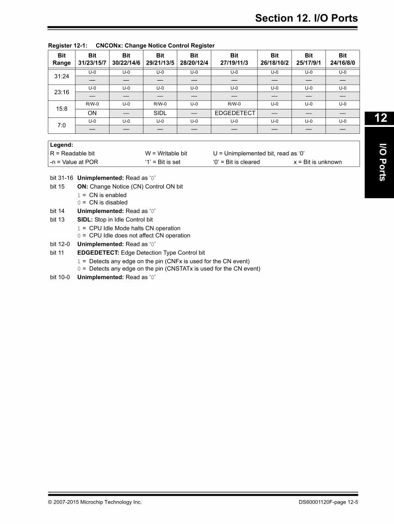
Register 12-1: CNCONx: Change Notice Control Register
Bit Range
Bit31/23/15/7
Bit30/22/14/6
Bit29/21/13/5
Bit28/20/12/4
Bit27/19/11/3
Bit26/18/10/2
Bit25/17/9/1
Bit24/16/8/0
31:24U-0 U-0 U-0 U-0 U-0 U-0 U-0 U-0
— — — — — — — —
23:16U-0 U-0 U-0 U-0 U-0 U-0 U-0 U-0
— — — — — — — —
15:8R/W-0 U-0 R/W-0 U-0 R/W-0 U-0 U-0 U-0
ON — SIDL — EDGEDETECT — — —
7:0U-0 U-0 U-0 U-0 U-0 U-0 U-0 U-0
— — — — — — — —
Legend:
R = Readable bit W = Writable bit U = Unimplemented bit, read as ‘0’
-n = Value at POR ‘1’ = Bit is set ‘0’ = Bit is cleared x = Bit is unknown
bit 31-16 Unimplemented: Read as ‘0’
bit 15 ON: Change Notice (CN) Control ON bit
1 = CN is enabled0 = CN is disabled
bit 14 Unimplemented: Read as ‘0’
bit 13 SIDL: Stop in Idle Control bit
1 = CPU Idle Mode halts CN operation0 = CPU Idle does not affect CN operation
bit 12-0 Unimplemented: Read as ‘0’
bit 11 EDGEDETECT: Edge Detection Type Control bit
1 = Detects any edge on the pin (CNFx is used for the CN event)0 = Detects any edge on the pin (CNSTATx is used for the CN event)
bit 10-0 Unimplemented: Read as ‘0’
© 2007-2015 Microchip Technology Inc. DS60001120F-page 12-5
PIC32 Family Reference Manual
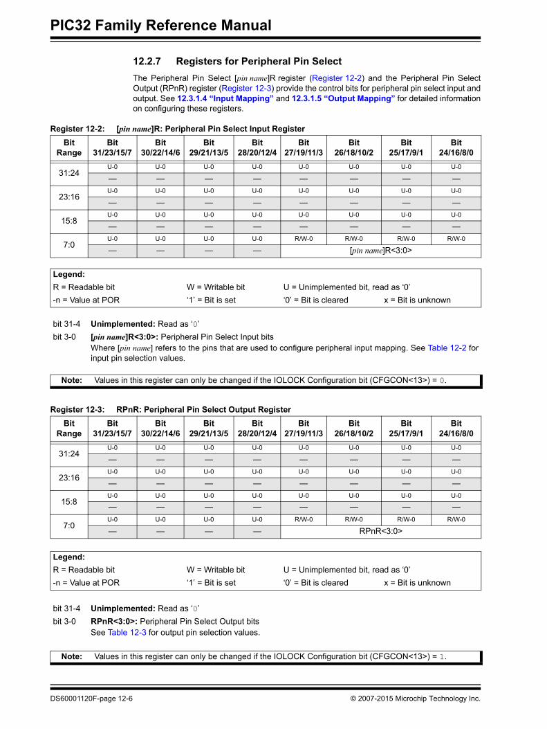
12.2.7 Registers for Peripheral Pin Select
The Peripheral Pin Select [pin name]R register (Register 12-2) and the Peripheral Pin Select Output (RPnR) register (Register 12-3) provide the control bits for peripheral pin select input and output. See 12.3.1.4 “Input Mapping” and 12.3.1.5 “Output Mapping” for detailed information on configuring these registers.
Register 12-2: [pin name]R: Peripheral Pin Select Input Register
Bit Range
Bit31/23/15/7
Bit30/22/14/6
Bit29/21/13/5
Bit28/20/12/4
Bit27/19/11/3
Bit26/18/10/2
Bit25/17/9/1
Bit24/16/8/0
31:24U-0 U-0 U-0 U-0 U-0 U-0 U-0 U-0
— — — — — — — —
23:16U-0 U-0 U-0 U-0 U-0 U-0 U-0 U-0
— — — — — — — —
15:8U-0 U-0 U-0 U-0 U-0 U-0 U-0 U-0
— — — — — — — —
7:0U-0 U-0 U-0 U-0 R/W-0 R/W-0 R/W-0 R/W-0
— — — — [pin name]R<3:0>
Legend:
R = Readable bit W = Writable bit U = Unimplemented bit, read as ‘0’
-n = Value at POR ‘1’ = Bit is set ‘0’ = Bit is cleared x = Bit is unknown
bit 31-4 Unimplemented: Read as ‘0’
bit 3-0 [pin name]R<3:0>: Peripheral Pin Select Input bitsWhere [pin name] refers to the pins that are used to configure peripheral input mapping. See Table 12-2 for input pin selection values.
Note: Values in this register can only be changed if the IOLOCK Configuration bit (CFGCON<13>) = 0.
Register 12-3: RPnR: Peripheral Pin Select Output Register
Bit Range
Bit31/23/15/7
Bit30/22/14/6
Bit29/21/13/5
Bit28/20/12/4
Bit27/19/11/3
Bit26/18/10/2
Bit25/17/9/1
Bit24/16/8/0
31:24U-0 U-0 U-0 U-0 U-0 U-0 U-0 U-0
— — — — — — — —
23:16U-0 U-0 U-0 U-0 U-0 U-0 U-0 U-0
— — — — — — — —
15:8U-0 U-0 U-0 U-0 U-0 U-0 U-0 U-0
— — — — — — — —
7:0U-0 U-0 U-0 U-0 R/W-0 R/W-0 R/W-0 R/W-0
— — — — RPnR<3:0>
Legend:
R = Readable bit W = Writable bit U = Unimplemented bit, read as ‘0’
-n = Value at POR ‘1’ = Bit is set ‘0’ = Bit is cleared x = Bit is unknown
bit 31-4 Unimplemented: Read as ‘0’
bit 3-0 RPnR<3:0>: Peripheral Pin Select Output bitsSee Table 12-3 for output pin selection values.
Note: Values in this register can only be changed if the IOLOCK Configuration bit (CFGCON<13>) = 1.
DS60001120F-page 12-6 © 2007-2015 Microchip Technology Inc.
Section 12. I/O PortsI/O
Po
rts
12
12.2.8 Set, Clear, and Invert I/O Port Registers
Every I/O module register has a corresponding SET, CLR, and INV register, which provide atomic bit manipulations. As the name of the register implies, a value written to a SET, CLR, or INV register effectively performs the implied operation, but only on the corresponding base register and only bits specified as ‘1’ are modified. Bits specified as ‘0’ are not modified.
• Writing 0x0001 to TRISASET register sets only bit 0 in the base register TRISA
• Writing 0x0020 to PORTDCLR register clears only bit 5 in the base register PORTD
• Writing 0x9000 to LATCINV register inverts only bits 15 and 12 in the base register LATC
Reading SET, CLR, and INV registers returns an undefined value. To see the affects of a write operation to a SET, CLR, or INV register, the base register must be read instead.
A typical method to toggle an I/O pin requires a read-modify-write operation performed on a PORTx register in software. For example, a read from a PORTx register, mask and modify the desired output bit or bits, and write the resulting value back to the PORTx register. This method is vulnerable to a read-modify-write issue where the port value may change after it is read and before the modified data can be written back, thus changing the previous state. This method also requires more instructions.
PORTA ^ = 0x0001;
A more efficient and atomic method uses the PORTxINV register. A write to the PORTxINV register effectively performs a read-modify-write operation on the target base register, equivalent to the software operation described previously; however, it is done in hardware. To toggle an I/O pin using this method, a ‘1’ is written to the corresponding bit in the PORTxINV register. This operation will read the PORTx register, invert only those bits specified as ‘1’, and write the resulting value to the LATx register, thus toggling the corresponding I/O pins all in a single atomic instruction cycle.
PORTAINV = 0x0001;
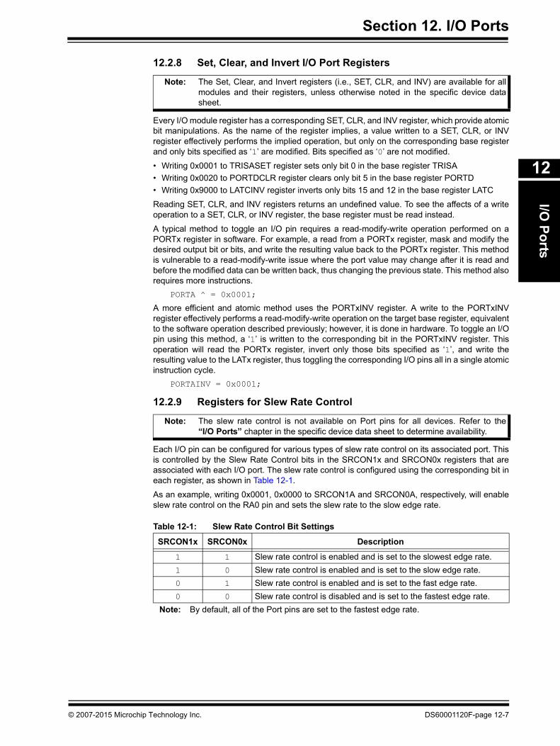
12.2.9 Registers for Slew Rate Control
Each I/O pin can be configured for various types of slew rate control on its associated port. This is controlled by the Slew Rate Control bits in the SRCON1x and SRCON0x registers that are associated with each I/O port. The slew rate control is configured using the corresponding bit in each register, as shown in Table 12-1.
As an example, writing 0x0001, 0x0000 to SRCON1A and SRCON0A, respectively, will enable slew rate control on the RA0 pin and sets the slew rate to the slow edge rate.
Table 12-1: Slew Rate Control Bit Settings
Note: The Set, Clear, and Invert registers (i.e., SET, CLR, and INV) are available for all modules and their registers, unless otherwise noted in the specific device data sheet.
Note: The slew rate control is not available on Port pins for all devices. Refer to the “I/O Ports” chapter in the specific device data sheet to determine availability.
SRCON1x SRCON0x Description
1 1 Slew rate control is enabled and is set to the slowest edge rate.
1 0 Slew rate control is enabled and is set to the slow edge rate.
0 1 Slew rate control is enabled and is set to the fast edge rate.
0 0 Slew rate control is disabled and is set to the fastest edge rate.
Note: By default, all of the Port pins are set to the fastest edge rate.
© 2007-2015 Microchip Technology Inc. DS60001120F-page 12-7

PIC32 Family Reference Manual
12.3 MODES OF OPERATION
12.3.1 Peripheral Pin Select (PPS)
A major challenge in general purpose devices is providing the largest possible set of peripheral features while minimizing the conflict of features on I/O pins. The challenge is even greater on low pin-count devices. In an application where more than one peripheral needs to be assigned to a single pin, inconvenient work arounds in application code or a complete redesign may be the only option.
Peripheral Pin Select (PPS) configuration provides an alternative to these choices by enabling peripheral set selection and their placement on a wide range of I/O pins. By increasing the pinout options available on a particular device, users can tailor the device to their entire application, rather than trimming the application to fit the device.
The PPS configuration feature operates over a fixed subset of digital I/O pins. Users may inde-pendently map the input and/or output of most digital peripherals to these I/O pins. PPS is per-formed in software and generally does not require the device to be reprogrammed. Hardware safeguards are included that prevent accidental or spurious changes to the peripheral mapping once it has been established.
12.3.1.1 AVAILABLE PINS
The number of available pins is dependent on the particular device and its pin count. Pins that support the PPS feature include the designation “RPn” in their full pin designation, where “RP” designates a remappable peripheral and “n” is the remappable port number.
12.3.1.2 AVAILABLE PERIPHERALS
The peripherals managed by the PPS are all digital-only peripherals. These include general serial communications (UART and SPI), general purpose timer clock inputs, timer-related peripherals (Input Capture and Output Compare) and interrupt-on-change inputs.
In comparison, some digital-only peripheral modules are never included in the PPS feature. This is because the peripheral’s function requires special I/O circuitry on a specific port and cannot be easily connected to multiple pins. These modules include I2C among others. A similar requirement excludes all modules with analog inputs, such as the ADC.
A key difference between remappable and non-remappable peripherals is that remappable peripherals are not associated with a default I/O pin. The peripheral must always be assigned to a specific I/O pin before it can be used. In contrast, non-remappable peripherals are always available on a default pin, assuming that the peripheral is active and not conflicting with another peripheral.
When a remappable peripheral is active on a given I/O pin, it takes priority over all other digital I/O and digital communication peripherals associated with the pin. Priority is given regardless of the type of peripheral that is mapped. Remappable peripherals never take priority over any analog functions associated with the pin.
12.3.1.3 CONTROLLING PPS
PPS features are controlled through two sets of Special Function Registers (SFRs): one to map peripheral inputs, and one to map outputs. Because they are separately controlled, a particular peripheral’s input and output (if the peripheral has both) can be placed on any selectable function pin without constraint.
The association of a peripheral to a peripheral-selectable pin is handled in two different ways, depending on whether an input or output is being mapped.
Note: Refer to the “I/O Ports” chapter in the specific device data sheet to determine availability.
DS60001120F-page 12-8 © 2007-2015 Microchip Technology Inc.

Section 12. I/O PortsI/O
Po
rts
12
12.3.1.4 INPUT MAPPING
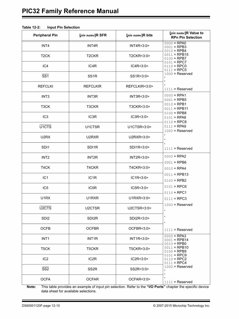
The inputs of the PPS options are mapped on the basis of the peripheral. That is, a control register associated with a peripheral dictates the pin it will be mapped to. The [pin name]R registers, where [pin name] refers to the peripheral pins listed in Table 12-2, are used to configure peripheral input mapping (see Register 12-2). Each register contains a set of four bit fields. Programming these bit fields with an appropriate value, maps the RPn pin with the corresponding value to that peripheral. Table 12-2 provides an example of the valid range of values for any bit field.
For example, Figure 12-2 illustrates the remappable pin selection for the U1RX input.
Figure 12-2: Remappable Input Example for U1RX
Note: Refer to the “I/O Ports” chapter in the specific device data sheet for the available input pin selections.
RPA2
RPB6
RPA4
0
1
2 U1RX input
U1RXR<3:0>
to peripheral
RPn
n
Note: For input only, PPS functionality does not have priority over TRISx settings. Therefore, when configuring RPn pin for input, the corresponding bit in the TRISx register must also be configured for input (set to ‘1’).
© 2007-2015 Microchip Technology Inc. DS60001120F-page 12-9
PIC32 Family Reference Manual
Table 12-2: Input Pin Selection
Peripheral Pin [pin name]R SFR [pin name]R bits[pin name]R Value to RPn Pin Selection
INT4 INT4R INT4R<3:0>0000 = RPA00001 = RPB30010 = RPB40011 = RPB150100 = RPB70101 = RPC70110 = RPC00111 = RPC51000 = Reserved•••
1111 = Reserved
T2CK T2CKR T2CKR<3:0>
IC4 IC4R IC4R<3:0>
SS1 SS1R SS1R<3:0>
REFCLKI REFCLKIR REFCLKIR<3:0>
INT3 INT3R INT3R<3:0> 0000 = RPA10001 = RPB50010 = RPB10011 = RPB110100 = RPB80101 = RPA80110 = RPC80111 = RPA91000 = Reserved•
•
•
1111 = Reserved
T3CK T3CKR T3CKR<3:0>
IC3 IC3R IC3R<3:0>
U1CTS U1CTSR U1CTSR<3:0>
U2RX U2RXR U2RXR<3:0>
SDI1 SDI1R SDI1R<3:0>
INT2 INT2R INT2R<3:0> 0000 = RPA2
0001 = RPB6
0010 = RPA4
0011 = RPB13
0100 = RPB2
0101 = RPC6
0110 = RPC1
0111 = RPC3
1000 = Reserved
•
•
•
1111 = Reserved
T4CK T4CKR T4CKR<3:0>
IC1 IC1R IC1R<3:0>
IC5 IC5R IC5R<3:0>
U1RX U1RXR U1RXR<3:0>
U2CTS U2CTSR U2CTSR<3:0>
SDI2 SDI2R SDI2R<3:0>
OCFB OCFBR OCFBR<3:0>
INT1 INT1R INT1R<3:0>0000 = RPA30001 = RPB140010 = RPB00011 = RPB100100 = RPB90101 = RPC90110 = RPC20111 = RPC41000 = Reserved•••
1111 = Reserved
T5CK T5CKR T5CKR<3:0>
IC2 IC2R IC2R<3:0>
SS2 SS2R SS2R<3:0>
OCFA OCFAR OCFAR<3:0>
Note: This table provides an example of input pin selection. Refer to the “I/O Ports” chapter the specific device data sheet for available selections.
DS60001120F-page 12-10 © 2007-2015 Microchip Technology Inc.
Section 12. I/O PortsI/O
Po
rts
12
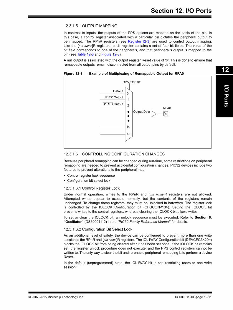
12.3.1.5 OUTPUT MAPPING
In contrast to inputs, the outputs of the PPS options are mapped on the basis of the pin. In this case, a control register associated with a particular pin dictates the peripheral output to be mapped. The RPnR registers (see Register 12-3) are used to control output mapping. Like the [pin name]R registers, each register contains a set of four bit fields. The value of the bit field corresponds to one of the peripherals, and that peripheral’s output is mapped to the pin (see Table 12-3 and Figure 12-3).
A null output is associated with the output register Reset value of ‘0’. This is done to ensure that remappable outputs remain disconnected from all output pins by default.
Figure 12-3: Example of Multiplexing of Remappable Output for RPA0
12.3.1.6 CONTROLLING CONFIGURATION CHANGES
Because peripheral remapping can be changed during run-time, some restrictions on peripheral remapping are needed to prevent accidental configuration changes. PIC32 devices include two features to prevent alterations to the peripheral map:
• Control register lock sequence
• Configuration bit select lock
12.3.1.6.1 Control Register Lock
Under normal operation, writes to the RPnR and [pin name]R registers are not allowed. Attempted writes appear to execute normally, but the contents of the registers remain unchanged. To change these registers, they must be unlocked in hardware. The register lock is controlled by the IOLOCK Configuration bit (CFGCON<13>). Setting the IOLOCK bit prevents writes to the control registers; whereas clearing the IOLOCK bit allows writes.
To set or clear the IOLOCK bit, an unlock sequence must be executed. Refer to Section 6. “Oscillator” (DS60001112) in the “PIC32 Family Reference Manual” for details.
12.3.1.6.2 Configuration Bit Select Lock
As an additional level of safety, the device can be configured to prevent more than one write session to the RPnR and [pin name]R registers. The IOL1WAY Configuration bit (DEVCFG3<29>) blocks the IOLOCK bit from being cleared after it has been set once. If the IOLOCK bit remains set, the register unlock procedure does not execute, and the PPS control registers cannot be written to. The only way to clear the bit and re-enable peripheral remapping is to perform a device Reset.
In the default (unprogrammed) state, the IOL1WAY bit is set, restricting users to one write session.
RPA0R<3:0>
0
15
1
Default
U1TX Output
U1RTS Output 2
14
Output DataRPA0
© 2007-2015 Microchip Technology Inc. DS60001120F-page 12-11

PIC32 Family Reference Manual
Table 12-3: Output Pin Selection
RPn Port Pin RPnR SFR RPnR bitsRPnR Value to Peripheral
Selection
RPA0 RPA0R RPA0R<3:0> 0000 = No Connect0001 = U1TX0010 = U2RTS0011 = SS10100 = Reserved0101 = OC10110 = Reserved0111 = C2OUT1000 = Reserved•••1111 = Reserved
RPB3 RPB3R RPB3R<3:0>
RPB4 RPB4R RPB4R<3:0>
RPB15 RPB15R RPB15R<3:0>
RPB7 RPB7R RPB7R<3:0>
RPC7 RPC7R RPC7R<3:0>
RPC0 RPC0R RPC0R<3:0>
RPC5 RPC5R RPC5R<3:0>
RPA1 RPA1R RPA1R<3:0> 0000 = No Connect0001 = Reserved0010 = Reserved0011 = SDO10100 = SDO20101 = OC20110 = Reserved•
•
•
1111 = Reserved
RPB5 RPB5R RPB5R<3:0>
RPB1 RPB1R RPB1R<3:0>
RPB11 RPB11R RPB11R<3:0>
RPB8 RPB8R RPB8R<3:0>
RPA8 RPA8R RPA8R<3:0>
RPC8 RPC8R RPC8R<3:0>
RPA9 RPA9R RPA9R<3:0>
RPA2 RPA2R RPA2R<3:0> 0000 = No Connect0001 = Reserved0010 = Reserved0011 = SDO10100 = SDO20101 = OC40110 = OC50111 = REFCLKO1000 = Reserved•••
1111 = Reserved
RPB6 RPB6R RPB6R<3:0>
RPA4 RPA4R RPA4R<3:0>
RPB13 RPB13R RPB13R<3:0>
RPB2 RPB2R RPB2R<3:0>
RPC6 RPC6R RPC6R<3:0>
RPC1 RPC1R RPC1R<3:0>
RPC3 RPC3R RPC3R<3:0>
RPA3 RPA3R RPA3R<3:0> 0000 = No Connect0001 = U1RTS0010 = U2TX0011 = Reserved0100 = SS20101 = OC30110 = Reserved0111 = C1OUT1000 = Reserved•
•
•
1111 = Reserved
RPB14 RPB14R RPB14R<3:0>
RPB0 RPB0R RPB0R<3:0>
RPB10 RPB10R RPB10R<3:0>
RPB9 RPB9R RPB9R<3:0>
RPC9 RPC9R RPC9R<3:0>
RPC2 RPC2R RPC2R<3:0>
RPC4 RPC4R RPC4R<3:0>
RPC3 RPC3R RPC3R<3:0>
Note: This table provides an example of output pin selection. Refer to the “I/O Ports” chapter in the specific device data sheet for available selections.
DS60001120F-page 12-12 © 2007-2015 Microchip Technology Inc.
Section 12. I/O PortsI/O
Po
rts
12
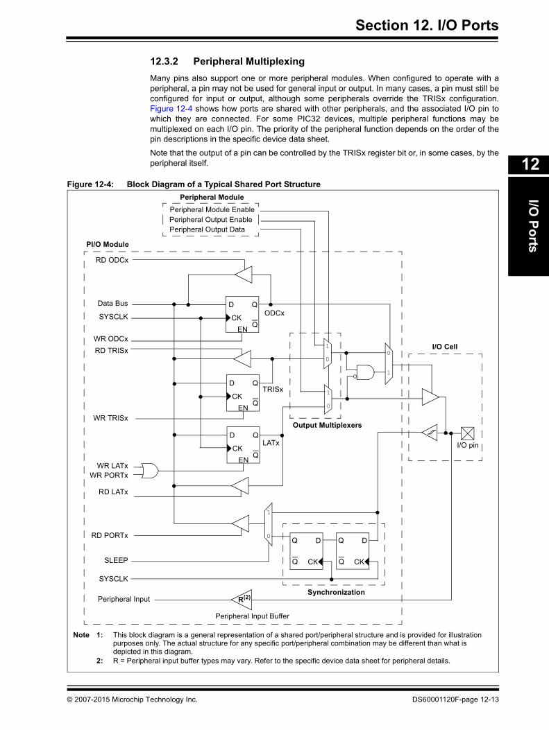
12.3.2 Peripheral Multiplexing
Many pins also support one or more peripheral modules. When configured to operate with a peripheral, a pin may not be used for general input or output. In many cases, a pin must still be configured for input or output, although some peripherals override the TRISx configuration. Figure 12-4 shows how ports are shared with other peripherals, and the associated I/O pin to which they are connected. For some PIC32 devices, multiple peripheral functions may be multiplexed on each I/O pin. The priority of the peripheral function depends on the order of the pin descriptions in the specific device data sheet.
Note that the output of a pin can be controlled by the TRISx register bit or, in some cases, by the peripheral itself.
Figure 12-4: Block Diagram of a Typical Shared Port Structure
Peripheral Output Data
Peripheral Module
Peripheral Output Enable
PI/O Module
Peripheral Module Enable
WR LATx
I/O pin
WR PORTx
Data Bus
RD LATx
RD PORTx
RD TRISx
WR TRISx
0
1
RD ODCx
SYSCLK
QD
CK
ENQ
QD
CK
ENQ
QD
CK
ENQ
Q D
CKQ
Q D
CKQ
0
1
SYSCLK
WR ODCx
ODCx
TRISx
LATx
SLEEP
1
0
1
0
Output Multiplexers
I/O Cell
SynchronizationR(2)Peripheral Input
Note 1: This block diagram is a general representation of a shared port/peripheral structure and is provided for illustration purposes only. The actual structure for any specific port/peripheral combination may be different than what is depicted in this diagram.
2: R = Peripheral input buffer types may vary. Refer to the specific device data sheet for peripheral details.
Peripheral Input Buffer
© 2007-2015 Microchip Technology Inc. DS60001120F-page 12-13
PIC32 Family Reference Manual
12.3.2.1 MULTIPLEXED DIGITAL INPUT PERIPHERAL
The following conditions are characteristic of a multiplexed digital input peripheral:
• Peripheral does not control the TRISx register. Some peripherals require the pin be configured as an input by setting the corresponding TRISx bit = 1
• Peripheral input path is independent of I/O input path and uses an input buffer that is dependent on the peripheral
• PORTx register data input path is not affected and is able to read the pin value
12.3.2.2 MULTIPLEXING DIGITAL OUTPUT PERIPHERAL
The following conditions are characteristic of a multiplexed digital output peripheral:
• Peripheral controls the output data. Some peripherals require the pin be configured as an output by setting the corresponding TRISx bit = 0
• If a peripheral pin has an automatic tri-state feature (e.g., PWM outputs), the peripheral has the ability to tri-state the pin
• Pin output driver type could be affected by peripheral (e.g., drive strength, slew rate, etc.)
• PORTx register output data has no effect
12.3.2.3 MULTIPLEXING DIGITAL BIDIRECTIONAL PERIPHERAL
The following conditions are characteristic of a multiplexed digital bidirectional peripheral:
• Peripheral automatically configures the pin as an output, but not as an input. Some peripherals require the pin be configured as an input by setting the corresponding TRISx bit = 1
• Peripherals control output data
• Pin output driver type could be affected by peripheral (e.g., drive strength, slew rate, etc.)
• PORTx register data input path is not affected and is able to read the pin value
• PORTx register output data has no effect
12.3.2.4 MULTIPLEXING ANALOG INPUT PERIPHERAL
The following condition is characteristic of a multiplexed analog input peripheral:
All digital port input buffers are disabled and PORTx registers read ‘0’ to prevent “crowbar”current.
12.3.2.5 MULTIPLEXING ANALOG OUTPUT PERIPHERAL
The following conditions are characteristic of a multiplexed analog output peripheral:
• All digital port input buffers are disabled and PORTx registers read ‘0’ to prevent crowbar current
• Analog output is driven onto the pin independent of the associated TRISx setting
12.3.2.6 SOFTWARE INPUT PIN CONTROL
Some of the functions assigned to an I/O pin may be input functions that do not take control of the pin output driver. An example of one such peripheral is the Input Capture module. If the I/O pin associated with the input capture is configured as an output, using the appropriate TRISx control bit, the user can manually affect the state of the input capture pin through its corresponding LATx register. This behavior can be useful in some situations, especially for testing purposes, when no external signal is connected to the input pin.
As shown previously in Figure 12-4, the organization of the peripheral multiplexers determines whether the peripheral input pin can be manipulated in software using the PORTx register. The conceptual peripherals shown in this figure disconnect the PORTx data from the I/O pin when the peripheral function is enabled.
Note: To use pins that are multiplexed with the ADC module for digital I/O, the corresponding bits in the AD1PCFG register, if present, must be set to ‘1’, even if the ADC module is turned OFF.
DS60001120F-page 12-14 © 2007-2015 Microchip Technology Inc.
Section 12. I/O PortsI/O
Po
rts
12
In general, the following peripherals allow their input pins to be controlled manually through the LATx registers:
• External Interrupts pins
• Input Capture pins
• Timer Clock input pins
• PWM Fault pins
Most serial communication peripherals, when enabled, take full control of the I/O pin so that the input pins associated with the peripheral cannot be affected through the corresponding PORTxregisters. These peripherals include the following modules:
• SPI
• I2C
• UART
12.3.3 Change Notice (CN) Pins
The CN pins provide PIC32 devices the ability to generate interrupt requests to the processor in response to a change of state on selected input pins (corresponding TRISx bits must be = 1). The total number of available CN inputs is dependent on the selected PIC32 device. Refer to the “I/O Ports” chapter in the specific device data sheet for further details.
The enabled pin values are compared with the values sampled during the last read operation of the designated PORTx register. If the pin value is different from the last value read, a mismatch condition is generated. The mismatch condition can occur on any of the enabled input pins. The mismatches are “ORed” together to provide a single interrupt-on-change signal. The enabled pins are sampled on every internal system clock cycle, SYSCLK.
12.3.3.1 CN CONFIGURATION AND OPERATION
The CN pins are configured as follows:
1. Disable CPU interrupts.
2. Set the desired CN I/O pin as an input by setting the corresponding TRISx register bits = 1.
3. Enable the CN Module by setting the ON bit (CNCONx<15>) = 1.
4. Enable individual CN input pins, enable optional pull-ups or pull-downs.5. Read the corresponding PORTx registers to clear the CN interrupt.6. Configure the CN Interrupt Priority bits, CNIP<2:0> (IPC6<20:18>), and Sub-priority bits,
CNIS<1:0> (IPC6<17:16>).
7. Clear the CN Interrupt Flag bit, by setting the CNIF bit (IFS1<0>) = 0.
8. Configure the CN pin interrupt for a specific edge detect using the EDGEDETECT bit in the CNCONx register, and set up edge control using the CNENx/CNNEx bits.
9. Enable the CN Interrupt Enable bit, by setting the CNIE bit (IEC1<0>) = 1.
10. Enable CPU interrupts.
The CNSTATx/CNFx registers indicate whether a change occurred on the corresponding pin since the last read of the PORTx bit. The CNFx registers indicate which type. When a CN interrupt occursin Mismatch mode, the user should read the PORTx register associated with the CN pins. This will clear the mismatch condition and set up the CN logic to detect the next pin change. The current PORTx value can be compared to the PORTx read value obtained at the last CN interrupt or during initialization, and used to determine which pin is changed. In Edge Detect mode, a CN interrupt can be controlled to occur only during a rising or falling edge condition on a pin. The CN pins have a minimum input pulse-width specification. Refer to the “Electrical Characteristics” chapter of the specific device data sheet to learn more.
Note: If the I/O pin is shared with an analog peripheral, it may be necessary to configure this pin as digital input.
© 2007-2015 Microchip Technology Inc. DS60001120F-page 12-15
PIC32 Family Reference Manual
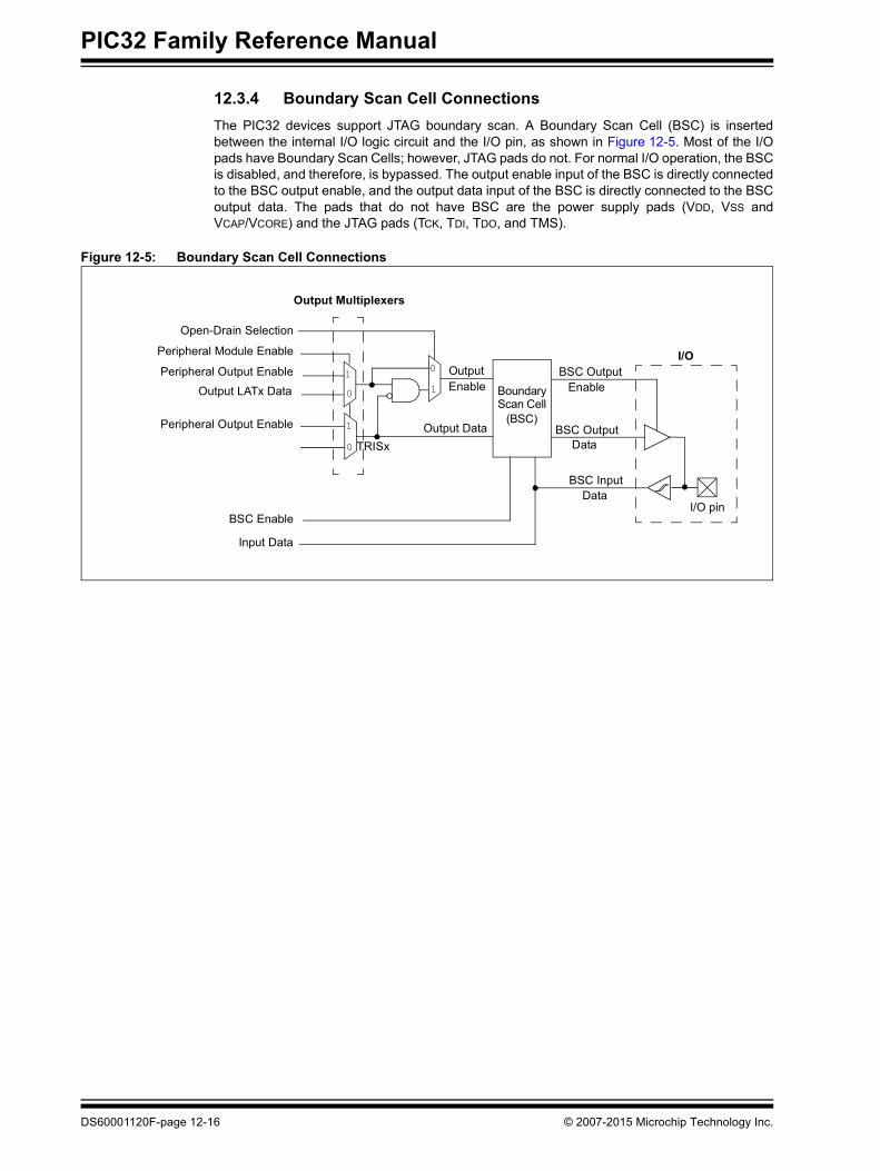
12.3.4 Boundary Scan Cell Connections
The PIC32 devices support JTAG boundary scan. A Boundary Scan Cell (BSC) is inserted between the internal I/O logic circuit and the I/O pin, as shown in Figure 12-5. Most of the I/O pads have Boundary Scan Cells; however, JTAG pads do not. For normal I/O operation, the BSC is disabled, and therefore, is bypassed. The output enable input of the BSC is directly connected to the BSC output enable, and the output data input of the BSC is directly connected to the BSC output data. The pads that do not have BSC are the power supply pads (VDD, VSS and VCAP/VCORE) and the JTAG pads (TCK, TDI, TDO, and TMS).
Figure 12-5: Boundary Scan Cell Connections
I/O pin
1
0
1
0
I/OPeripheral Output Enable
Output Multiplexers
Peripheral Module Enable
BoundaryScan Cell
(BSC)
BSC Input
BSC Enable
0
1
Output Enable
Output Data
BSC Output Enable
BSC OutputData
Peripheral Output Enable
Input Data
Output LATx Data
TRISx
Data
Open-Drain Selection
DS60001120F-page 12-16 © 2007-2015 Microchip Technology Inc.
Section 12. I/O PortsI/O
Po
rts
12
12.4 OPERATION IN POWER-SAVING MODES
12.4.1 I/O Port Operation in Sleep Mode
As the device enters Sleep mode, the system clock is disabled; however, the CN module continues to operate. If one of the enabled CN pins changes state, the CNIF bit (IFS1<0>) will be set. If the CNIE bit (IEC1<0>) is set, and its priority is greater than current CPU priority, the device will wake from Sleep (or Idle) mode and execute the CN Interrupt Service Routine.
If the assigned priority level of the CN interrupt is less than or equal to the current CPU priority level, the CPU will not be awakened and the device will enter Idle mode.
12.4.2 I/O Port Operation in Idle Mode
As the device enters Idle mode, the system clock sources remain functional. The SIDL bit (CNCONx<13>) selects whether the module will stop or continue functioning in Idle mode.
• If SIDL = 1, the module will continue to sample Input CN I/O pins in Idle mode; however, synchronization is disabled
• If SIDL = 0, the module will continue to synchronize and sample Input CN I/O pins in Idle mode
12.5 EFFECTS OF VARIOUS RESETS
12.5.1 Device Reset
All I/O registers are forced to their reset states upon a device Reset.
12.5.2 Power-on Reset
All I/O registers are forced to their reset states upon a Power-on Reset (POR).
12.5.3 Watchdog Reset
All I/O registers are unchanged upon a Watchdog Reset.
© 2007-2015 Microchip Technology Inc. DS60001120F-page 12-17

PIC32 Family Reference Manual
12.6 RELATED APPLICATION NOTES
This section lists application notes that are related to this section of the manual. These application notes may not be written specifically for the PIC32 device family, but the concepts are pertinent and could be used with modification and possible limitations. The current application notes related to the I/O Ports are:
Title Application Note #
No related application notes at this time N/A
Note: Please visit the Microchip web site (http://www.microchip.com) for additional application notes and code examples for the PIC32 family of devices.
DS60001120F-page 12-18 © 2007-2015 Microchip Technology Inc.
Section 12. I/O PortsI/O
Po
rts
12
12.7 REVISION HISTORY
Revision A (August 2007)
This is the initial released version of this document.
Revision B (October 2007)
Updated document to remove Confidential status.
Revision C (April 2008)
Revised status to Preliminary; Revised U-0 to r-x; Revised Register 12-13; Revised Figure 12-1 and 12-2.
Revision D (May 2008)
Revised Register 12-17, add note to FRZ; Add note to Registers 12-19, 12-30, 12-31; Revised Example 12-1 and 12-2; Change Reserved bits from “Maintain as” to “Write”; Added Note to ON bit (CNCONx Register).
Revision E (July 2011)
This revision includes the following changes:
• Added a note at the beginning of the section, which provides information on complementary documentation
• Changed all occurrences of PIC32MX to PIC32
• Removed the paragraph about the I/O related SFRs in 12.1 “Introduction”
• Added 12.2.7 “Registers for Peripheral Pin Select”
• Removed all Interrupt registers
• Removed TRISx, PORTx, LATx, ODCx, CNEN, CNPUE registers and their associated SET, INV, and CLR registers
• Removed the FRZ bit from the Change Notice Control register (see Register 12-1)
• Removed related Interrupts section and sub-sections
• Removed the operation of the I/O port in Debug mode from 12.4 “Operation in Power-Saving Modes”
• Removed I/O Port Application, I/O Pin Control and Design Tips sections
• Removed 12.2.6 CN Control Registers section
• Renamed the section 12.2.5 ODCx Registers as 12.2.4 “Registers for Open-Drain Con-figuration (ODCx)”
• Added section 12.2.5 “Registers for Configuring Analog and Digital Port Pins (ANSELx)”
• Added section 12.2.6 “Registers for Input Change Notification”
• Added section 12.3.1 “Peripheral Pin Select (PPS)”
• In 12.3 “Modes of Operation”, removed sections on Digital Inputs, Analog Inputs, Digital Outputs, Analog Outputs, Open-Drain Configuration and Port Descriptions
• Updated the note in the second point of 12.3.3.1 “CN Configuration and Operation”
• Modifications to register formatting and minor updates have been made throughout the document
Revision F (January 2015)
This revision includes the following updates:
• Added 12.2.9 “Registers for Slew Rate Control”
• 12.3.3.1 “CN Configuration and Operation” was updated
• Minor updates to text and formatting were incorporated throughout the document
© 2007-2015 Microchip Technology Inc. DS60001120F-page 12-19
PIC32 Family Reference Manual
NOTES:
DS60001120F-page 12-20 © 2007-2015 Microchip Technology Inc.
Note the following details of the code protection feature on Microchip devices:
• Microchip products meet the specification contained in their particular Microchip Data Sheet.
• Microchip believes that its family of products is one of the most secure families of its kind on the market today, when used in the intended manner and under normal conditions.
• There are dishonest and possibly illegal methods used to breach the code protection feature. All of these methods, to our knowledge, require using the Microchip products in a manner outside the operating specifications contained in Microchip’s Data Sheets. Most likely, the person doing so is engaged in theft of intellectual property.
• Microchip is willing to work with the customer who is concerned about the integrity of their code.
• Neither Microchip nor any other semiconductor manufacturer can guarantee the security of their code. Code protection does not mean that we are guaranteeing the product as “unbreakable.”
Code protection is constantly evolving. We at Microchip are committed to continuously improving the code protection features of our products. Attempts to break Microchip’s code protection feature may be a violation of the Digital Millennium Copyright Act. If such acts allow unauthorized access to your software or other copyrighted work, you may have a right to sue for relief under that Act.
Information contained in this publication regarding device applications and the like is provided only for your convenience and may be superseded by updates. It is your responsibility to ensure that your application meets with your specifications. MICROCHIP MAKES NO REPRESENTATIONS OR WARRANTIES OF ANY KIND WHETHER EXPRESS OR IMPLIED, WRITTEN OR ORAL, STATUTORY OR OTHERWISE, RELATED TO THE INFORMATION, INCLUDING BUT NOT LIMITED TO ITS CONDITION, QUALITY, PERFORMANCE, MERCHANTABILITY OR FITNESS FOR PURPOSE. Microchip disclaims all liability arising from this information and its use. Use of Microchip devices in life support and/or safety applications is entirely at the buyer’s risk, and the buyer agrees to defend, indemnify and hold harmless Microchip from any and all damages, claims, suits, or expenses resulting from such use. No licenses are conveyed, implicitly or otherwise, under any Microchip intellectual property rights.
2007-2015 Microchip Technology Inc.
QUALITY MANAGEMENT SYSTEM CERTIFIED BY DNV
== ISO/TS 16949 ==
Trademarks
The Microchip name and logo, the Microchip logo, dsPIC, FlashFlex, flexPWR, JukeBlox, KEELOQ, KEELOQ logo, Kleer, LANCheck, MediaLB, MOST, MOST logo, MPLAB, OptoLyzer, PIC, PICSTART, PIC32 logo, RightTouch, SpyNIC, SST, SST Logo, SuperFlash and UNI/O are registered trademarks of Microchip Technology Incorporated in the U.S.A. and other countries.
The Embedded Control Solutions Company and mTouch are registered trademarks of Microchip Technology Incorporated in the U.S.A.
Analog-for-the-Digital Age, BodyCom, chipKIT, chipKIT logo, CodeGuard, dsPICDEM, dsPICDEM.net, ECAN, In-Circuit Serial Programming, ICSP, Inter-Chip Connectivity, KleerNet, KleerNet logo, MiWi, MPASM, MPF, MPLAB Certified logo, MPLIB, MPLINK, MultiTRAK, NetDetach, Omniscient Code Generation, PICDEM, PICDEM.net, PICkit, PICtail, RightTouch logo, REAL ICE, SQI, Serial Quad I/O, Total Endurance, TSHARC, USBCheck, VariSense, ViewSpan, WiperLock, Wireless DNA, and ZENA are trademarks of Microchip Technology Incorporated in the U.S.A. and other countries.
SQTP is a service mark of Microchip Technology Incorporated in the U.S.A.
Silicon Storage Technology is a registered trademark of Microchip Technology Inc. in other countries.
GestIC is a registered trademarks of Microchip Technology Germany II GmbH & Co. KG, a subsidiary of Microchip Technology Inc., in other countries.
All other trademarks mentioned herein are property of their respective companies.
© 2007-2015, Microchip Technology Incorporated, Printed in the U.S.A., All Rights Reserved.
ISBN: 978-1-63276-835-3
DS60001120F-page 12 -21
Microchip received ISO/TS-16949:2009 certification for its worldwide headquarters, design and wafer fabrication facilities in Chandler and Tempe, Arizona; Gresham, Oregon and design centers in California and India. The Company’s quality system processes and procedures are for its PIC® MCUs and dsPIC® DSCs, KEELOQ® code hopping devices, Serial EEPROMs, microperipherals, nonvolatile memory and analog products. In addition, Microchip’s quality system for the design and manufacture of development systems is ISO 9001:2000 certified.
DS60001120F-page 12-22 2007-2015 Microchip Technology Inc.
AMERICASCorporate Office2355 West Chandler Blvd.Chandler, AZ 85224-6199Tel: 480-792-7200 Fax: 480-792-7277Technical Support: http://www.microchip.com/supportWeb Address: www.microchip.com
AtlantaDuluth, GA Tel: 678-957-9614 Fax: 678-957-1455
Austin, TXTel: 512-257-3370
BostonWestborough, MA Tel: 774-760-0087 Fax: 774-760-0088
ChicagoItasca, IL Tel: 630-285-0071 Fax: 630-285-0075
ClevelandIndependence, OH Tel: 216-447-0464 Fax: 216-447-0643
DallasAddison, TX Tel: 972-818-7423 Fax: 972-818-2924
DetroitNovi, MI Tel: 248-848-4000
Houston, TX Tel: 281-894-5983
IndianapolisNoblesville, IN Tel: 317-773-8323Fax: 317-773-5453
Los AngelesMission Viejo, CA Tel: 949-462-9523 Fax: 949-462-9608
New York, NY Tel: 631-435-6000
San Jose, CA Tel: 408-735-9110
Canada - TorontoTel: 905-673-0699 Fax: 905-673-6509
ASIA/PACIFICAsia Pacific OfficeSuites 3707-14, 37th FloorTower 6, The GatewayHarbour City, KowloonHong KongTel: 852-2943-5100Fax: 852-2401-3431
Australia - SydneyTel: 61-2-9868-6733Fax: 61-2-9868-6755
China - BeijingTel: 86-10-8569-7000 Fax: 86-10-8528-2104
China - ChengduTel: 86-28-8665-5511Fax: 86-28-8665-7889
China - ChongqingTel: 86-23-8980-9588Fax: 86-23-8980-9500
China - Dongguan
Tel: 86-769-8702-9880
China - HangzhouTel: 86-571-8792-8115 Fax: 86-571-8792-8116
China - Hong Kong SARTel: 852-2943-5100 Fax: 852-2401-3431
China - NanjingTel: 86-25-8473-2460Fax: 86-25-8473-2470
China - QingdaoTel: 86-532-8502-7355Fax: 86-532-8502-7205
China - ShanghaiTel: 86-21-5407-5533 Fax: 86-21-5407-5066
China - ShenyangTel: 86-24-2334-2829Fax: 86-24-2334-2393
China - ShenzhenTel: 86-755-8864-2200 Fax: 86-755-8203-1760
China - WuhanTel: 86-27-5980-5300Fax: 86-27-5980-5118
China - XianTel: 86-29-8833-7252Fax: 86-29-8833-7256
ASIA/PACIFICChina - XiamenTel: 86-592-2388138 Fax: 86-592-2388130
China - ZhuhaiTel: 86-756-3210040 Fax: 86-756-3210049
India - BangaloreTel: 91-80-3090-4444 Fax: 91-80-3090-4123
India - New DelhiTel: 91-11-4160-8631Fax: 91-11-4160-8632
India - PuneTel: 91-20-3019-1500
Japan - OsakaTel: 81-6-6152-7160 Fax: 81-6-6152-9310
Japan - TokyoTel: 81-3-6880- 3770 Fax: 81-3-6880-3771
Korea - DaeguTel: 82-53-744-4301Fax: 82-53-744-4302
Korea - SeoulTel: 82-2-554-7200Fax: 82-2-558-5932 or 82-2-558-5934
Malaysia - Kuala LumpurTel: 60-3-6201-9857Fax: 60-3-6201-9859
Malaysia - PenangTel: 60-4-227-8870Fax: 60-4-227-4068
Philippines - ManilaTel: 63-2-634-9065Fax: 63-2-634-9069
SingaporeTel: 65-6334-8870Fax: 65-6334-8850
Taiwan - Hsin ChuTel: 886-3-5778-366Fax: 886-3-5770-955
Taiwan - KaohsiungTel: 886-7-213-7828
Taiwan - TaipeiTel: 886-2-2508-8600 Fax: 886-2-2508-0102
Thailand - BangkokTel: 66-2-694-1351Fax: 66-2-694-1350
EUROPEAustria - WelsTel: 43-7242-2244-39Fax: 43-7242-2244-393Denmark - CopenhagenTel: 45-4450-2828 Fax: 45-4485-2829
France - ParisTel: 33-1-69-53-63-20 Fax: 33-1-69-30-90-79
Germany - DusseldorfTel: 49-2129-3766400
Germany - MunichTel: 49-89-627-144-0 Fax: 49-89-627-144-44
Germany - PforzheimTel: 49-7231-424750
Italy - Milan Tel: 39-0331-742611 Fax: 39-0331-466781
Italy - VeniceTel: 39-049-7625286
Netherlands - DrunenTel: 31-416-690399 Fax: 31-416-690340
Poland - WarsawTel: 48-22-3325737
Spain - MadridTel: 34-91-708-08-90Fax: 34-91-708-08-91
Sweden - StockholmTel: 46-8-5090-4654
UK - WokinghamTel: 44-118-921-5800Fax: 44-118-921-5820
Worldwide Sales and Service
01/27/15