schottky diodes selection guide
TRANSCRIPT
R.F. elettronica di Rota F. www.rfmicrowave.it [email protected] tel ++39.02.99 48 75 15 fax ++39.02.99 48 92 76
SCHOTTKY DIODES ( HOT - CARRIER ) pag A 1
Schottky diodes selection guide
For HIGH SENSITIVITY , ZERO-BIAS or LOW BARRIER applications --- for lab detectors as RF detector with sweep generator --- RF fields detector, electromagnetic pollution, TAG , etc… --- passive or active mobile phones and bugs detector
diode TSS (tangential sensitivity)
Glass case
SMD case
Ceramic or special case
-59 dBm @ 2 GHz HSMS 2850 - 2851 SMS 7630
-55 dBm @ 10 GHz usable up to 18 GHz
these are the much sensitive diodes at ZERO BIAS
-53 dBm @ 2 GHz ND 4991 - 1SS276 DDC2353 -55 dBm @ 6 GHz LOW BARRIER up to 20 GHz from -54 dBm to -52 dBm up to 24 GHz depending on type
all BAT 15… types are LOW BARRIER high sensitivity vatious types available
-56 dBm @ 2 GHz with bias HP 5082-2824 HSMS.282…series low barrier, up to millimeter freq. beam lead version version with leads of the famous 1N21 - 23
1N821 point-contact silicon , up to 5 GHz
NOTE : high sensitivity silicon or germanium diodes for detectors are available too, see VARIOUS DIODES
for : RECEIVING MIXERS - RF DETECTORS - SAMPLING
freq. config. glass case SMD or plastic case ceramic case up to 500 MHz BAT 42 - 43 - 46 - 48 - 85 - 86 BAS 40-…- BAT 64-....
single 5082.2800 - BAT 45 - 82 - 83 HSCH 1001 HSMS 28.... , BAT 68
pair 5082.2804 BAS 70... , HSMS 28... up to 2 GHz
quad 5082.2836 ND 487C1-3R
single 5082.2810, 2811, 2817 2824, 2835, 2900, MA4853 ND4991 1SS154 ,BA 481, QSCH 5374
HSMS 2810 , 2820 BAT 17 , BAT 68
pair 5082.2826, 2912 HSMS 28….
up to
3 - 5
GHz quad HP 5082.2815, 2826 HSMS 2808 HP 5082.2830, 2831, 2231
single DC 1501EP - HSMS 2850 - 2851 BAT15... various types, BAT62-03W-02W
DC 1501E (max 18 GHz)
pair BAT 15-099 , BAT 62…. BAT 15 099 – MA4E 501
up to 6 - 12 GHz
quad HSMS 8207 + 8209 HP5082.2277, HSCH 6812 single 5082-2202, 2751, DC1304A, DH363up to
18 GHz pair HSMS 8202 - MA4E1245 ( 2 sel. diodes ) MA4E522, DH 340
up to 24 - 30
GHz single
BAT14-104 , MA4E 920 , MA40133 + BAT14-B beam lead case
> 20 GHz for bonding
beam - lead case
single: HSCH 9101 , DC 1308 , HSCH5340-DMB2856 , MA4E 2037 , BAT14-110S antiparallel: HSCH 9251, MA4E 997 pair: BAT 14-050D, 090D, BAT 15-090D, HSCH 5531 --- quad: MA4E400H
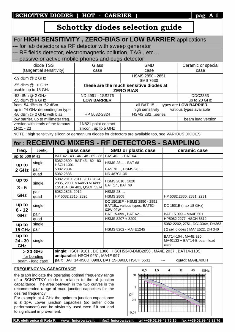
FREQUENCY Vs. CAPACITANCE
the graph indicate the operating optimal frequency range of a SCHOTTKY diode in relation to the of junction capacitance. The area between in the two curves is the recommended range of max. junction capacities for the desired frequency. For example at 4 GHz the optimum junction capacitance is ≤ 1pF. Lower junction capacities (so better diode performances) can be obviously used even if it not lead to significant improvement.
R.F. elettronica di Rota F. www.rfmicrowave.it [email protected] tel ++39.02.99 48 75 15 fax ++39.02.99 48 92 76
SCHOTTKY DIODES ( HOT - CARRIER ) pag A 2
glass case single diodes price € each CJ
pF VR V
VF V
CJ @ ØVR , CJ decreases a lot with bias or local oscillator VF @ 1mA NB typical values cod. 1+
pcs4+ pcs
10+pcs
2.2 60 HSCH-1001 = 1N 6263 0,70 0,65 0,60
2.2 60 SD 101A 0,70 0,62 0,55
2 70
0.38
they are similar types , up to 2 GHz suitable as detector and up to 1.5 GHz as mixer, HSCH1001-1N6263-SD101A are used also as protection for RX input in HF and VHF frequencies due to their low capacitance and low switching time
5082-2800 1N 5711 1,70 1,60 1,50
1.2 20 0.36general purpose, mixer and detector diode up to 3 GHz, it is also available in some SMD versions HSMS 281... type or with glass case 5082-2811
5082-2810 -- -- --
1.2 15 0.37 general purpose, mixer and detector diode up to 3 GHz 5082-2811 2,90 2,80 2,70
1 15 0.35this diode is a very good mixer and detector, it dissipates up to 1/4W to 200 °C, low Flicker noise 1/F with bias 20 uA and high Tss sensitivity -56dBm / 2GHz see AN hp 923 (HP 11$ )
5082-2824 2,60 2,50 2,40
1 8 0.34 up to 5 GHz, low noise mixer up to 3GHz = HSMS 282… 5082-2835 2,50 2,40 2,30
1.2 10 0.33 up to 3 GHz, very good performances as low noise mixer and low 1/F noise, see HP applic. notes ( HP list 4 $ ) 5082-2900 2,00 1,90 1,80
5 100 0.33 high voltage BAT46 (= BAT41) 0,40 0,36 0,33
7 30 0.28 high sensitivity and high current 200 mA BAT 42 0,30 0,27 0,256 30 0.30 high current up to 200 mA BAT 43 0,30 0,27 0,25
10 40 0,30 high current up to 350 mA BAT 48 0,30 0,26 0,238 30 0.28 high sensitivity BAT 85 0,25 0,22 0,207 50 0.28
for HF and VHF frequencies
detector , mixer , fast switch, etc…
high sensitivity BAT 86 0,25 0,22 0,201,4 50 0,38 up to 2 GHz , mixer and detector BAT 82 0,40 0,36 0,331.4 60 0.38 up to 2 GHz , mixer and detector BAT 83 0,40 0,36 0,331 6 0.35 up to 2-3 GHz , mixer and detector BAT 45 0,50 0,45 0,40
1 4 0.35 very good power detector up to 4 GHz, and mixer up to 2.5 GHz BA 481 0,50 0,45 0,40
0.7 3 0,26 very good mixer and detector up to 5 - 8 GHz QSCH 5374 4,80
0.8 ND 4991 5,30 4,90 4,70
LOW BARRIER
0.7
3
0.20
high sesitivity Tss = -55 dBm , suitable for laboratory detectors, it is similar to HP 423-HP8472 detector or as low LO level mixer up to 5 GHz . ND4991 is a good replacement to the input mixer diode for spectrum analyzer HP 141 HP 8554B up to 1.2 GHz and HP 8558 up to 1.5 GHz 1SS 276 5,00 4,50 4,50
matched pairs and matched quads
These Schottky diodes are provided as selected pairs, quads or in custom quantities. They are exactly the same as those supplied as single but they are matched to guarantee the same capacitance and forward voltage of all units, they can be used for example as mixers, sampling, multipliers, etc.... For the characteristics please refer to the original code of the single diode eg.: 5082-2836 = single type 5082-2800, those provided in custom matched quantity (2 or more units) have an accuracy within 0.1 pF of junction capacitance and 20 mV of forward voltage in the selection.
original diode as provided cod. price € 5082-2800 matched pair ∆VF = 20mV 5082-2804 3,60 / pair 5082-2800 custom matched quantity ∆VF = 20mV , ∆CJ = 0.1pF 5082-2836 1,80 / each
5082-2811 matched quad , spare part for sampling probe, HP3406A + Racal RF voltmeters, etc… 5082-2815 13,00 / quad
5082-2811 custom matched quantity ∆VF = 10mV , ∆CJ = 0.1pF 5082-2826 3,25 / each
5082-2900 matched pair ∆VF = 30mV ( HP list 8,50 $ ) 5082-2912 4,10 / pair
R.F. elettronica di Rota F. www.rfmicrowave.it [email protected] tel ++39.02.99 48 75 15 fax ++39.02.99 48 92 76
continue , SCHOTTKY DIODES ( HOT - CARRIER ) pag A 3
Matched quads in a single case ( ceramic or SMD )
These Schottky diodes, unlike to those reported in the previous page, are provided only as quad configuration but in a single case, of course they are internally matched quads
price € each configuration Cj
pF VR V
VF V
CJ @ ØVR , CJ decreases a lot with bias or local oscillator VF @ 1mA typical values
cod. 1+ pcs
4+ pcs
10+ pcs
ring cross-over 1 0.2 low barrier up to 2 GHz , cross-over ring , Nec ND-487C1-3R ND 487C1 3,00 2,85 2,65
0.4 0.35 up to 10 GHz Ct max 0.5 pF, ceramic case 5082-2277 3,50 3,30 3,10
0.5 0.4 up to 3 GHz , ceramic case 5082-2830 6,40
0.5 0.25 up to 3 GHz, low barrier, ceramic case 5082-2831 3,50 3,30 3,10
ring ( normal )
0.25 4 0.43 up to 12GHz, HI REL hermetic ceramic case HSCH-6812 16,00
bridge ( unconnected ) 1 15 0,30
2 couples of diodes in series, each cuople has the central tap in bridge quad configuration, for sampling up to 4 GHz or detector and voltage doubler RD 12 Ω , LifeTime 100<pS , ΔVf <15 mV , ΔCj <0.2 pF
HSMS-282P 1,20 1,05 0,90
ring cross-over 1 15 0,30 as mixer up to 4 GHz HSMS-2829 2,50
ring ( normal ) 0.2 4 0,30 HSMS-8207 4,30
ring cross-over 0.2 4 0,30
CT < 0.26 pF , ∆CT < 0.04 pF dynamic resistance < 14 Ω ∆ dynamic resistance < 2 Ω ∆VF < 20 mV , @ 12 GHz 6.3 dB conversion loss typ.
HSMS-8209 4,40
0.4 4 0.40 BAT-14-099R
BAT.. ring cross-over
0.4 4 0,25
these 2 diodes are pin compatible with HSMS 8209 , except for a little difference in forward voltage
BAT-15-099R
see HSMS-8209
R.F. elettronica di Rota F. www.rfmicrowave.it [email protected] tel ++39.02.99 48 75 15 fax ++39.02.99 48 92 76
continue , SCHOTTKY DIODES ( HOT - CARRIER ) pag A 4
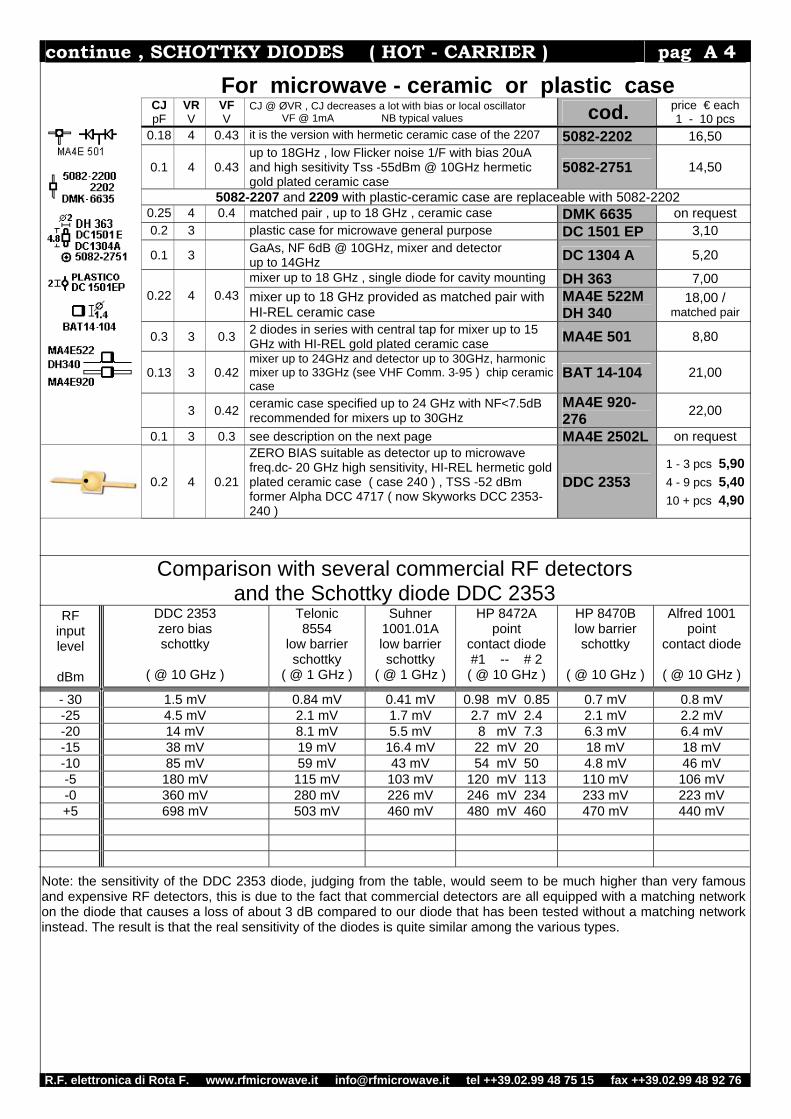
Comparison with several commercial RF detectors and the Schottky diode DDC 2353
RF input level
dBm
DDC 2353 zero bias schottky
( @ 10 GHz )
Telonic 8554
low barrier schottky
( @ 1 GHz )
Suhner 1001.01A low barrier schottky
( @ 1 GHz )
HP 8472A point
contact diode #1 -- # 2 ( @ 10 GHz )
HP 8470B low barrier schottky
( @ 10 GHz )
Alfred 1001 point
contact diode
( @ 10 GHz )
- 30 1.5 mV 0.84 mV 0.41 mV 0.98 mV 0.85 0.7 mV 0.8 mV -25 4.5 mV 2.1 mV 1.7 mV 2.7 mV 2.4 2.1 mV 2.2 mV -20 14 mV 8.1 mV 5.5 mV 8 mV 7.3 6.3 mV 6.4 mV -15 38 mV 19 mV 16.4 mV 22 mV 20 18 mV 18 mV -10 85 mV 59 mV 43 mV 54 mV 50 4.8 mV 46 mV -5 180 mV 115 mV 103 mV 120 mV 113 110 mV 106 mV -0 360 mV 280 mV 226 mV 246 mV 234 233 mV 223 mV +5 698 mV 503 mV 460 mV 480 mV 460 470 mV 440 mV
Note: the sensitivity of the DDC 2353 diode, judging from the table, would seem to be much higher than very famous and expensive RF detectors, this is due to the fact that commercial detectors are all equipped with a matching network on the diode that causes a loss of about 3 dB compared to our diode that has been tested without a matching network instead. The result is that the real sensitivity of the diodes is quite similar among the various types.
For microwave - ceramic or plastic case CJ pF
VR V
VF V
CJ @ ØVR , CJ decreases a lot with bias or local oscillator VF @ 1mA NB typical values cod. price € each
1 - 10 pcs 0.18 4 0.43 it is the version with hermetic ceramic case of the 2207 5082-2202 16,50
0.1 4 0.43up to 18GHz , low Flicker noise 1/F with bias 20uA and high sesitivity Tss -55dBm @ 10GHz hermetic gold plated ceramic case
5082-2751 14,50
5082-2207 and 2209 with plastic-ceramic case are replaceable with 5082-2202 0.25 4 0.4 matched pair , up to 18 GHz , ceramic case DMK 6635 on request 0.2 3 plastic case for microwave general purpose DC 1501 EP 3,10
0.1 3 GaAs, NF 6dB @ 10GHz, mixer and detector up to 14GHz DC 1304 A 5,20
mixer up to 18 GHz , single diode for cavity mounting DH 363 7,00 0.22 4 0.43 mixer up to 18 GHz provided as matched pair with
HI-REL ceramic case MA4E 522M DH 340
18,00 / matched pair
0.3 3 0.3 2 diodes in series with central tap for mixer up to 15 GHz with HI-REL gold plated ceramic case MA4E 501 8,80
0.13 3 0.42mixer up to 24GHz and detector up to 30GHz, harmonic mixer up to 33GHz (see VHF Comm. 3-95 ) chip ceramic case
BAT 14-104 21,00
3 0.42 ceramic case specified up to 24 GHz with NF<7.5dB
recommended for mixers up to 30GHz MA4E 920-276 22,00
0.1 3 0.3 see description on the next page MA4E 2502L on request
0.2 4 0.21
ZERO BIAS suitable as detector up to microwave freq.dc- 20 GHz high sensitivity, HI-REL hermetic gold plated ceramic case ( case 240 ) , TSS -52 dBm former Alpha DCC 4717 ( now Skyworks DCC 2353-240 )
DDC 2353 1 - 3 pcs 5,90
4 - 9 pcs 5,40
10 + pcs 4,90
R.F. elettronica di Rota F. www.rfmicrowave.it [email protected] tel ++39.02.99 48 75 15 fax ++39.02.99 48 92 76
continue , SCHOTTKY DIODES ( HOT - CARRIER ) pag A 5
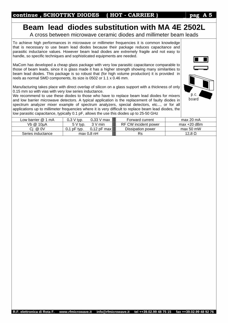
Beam lead diodes substitution with MA 4E 2502L A cross between microwave ceramic diodes and millimeter beam leads
To achieve high performances in microwave or millimeter frequencies it is common knowledge that is necessary to use beam lead diodes because their package reduces capacitance and parasitic inductance values. However beam lead diodes are extremely fragile and not easy to handle, so specific techniques and sophisticated equipments are needed. MaCom has developed a cheap glass package with very low parasitic capacitance comparable to those of beam leads, since it is glass made it has a higher strength showing many similarities to beam lead diodes. This package is so robust that (for high volume production) it is provided in reels as normal SMD components, its size is 0502 or 1.1 x 0.46 mm. Manufacturing takes place with direct overlap of silicon on a glass support with a thickness of only 0.15 mm so with vias with very low series inductance. We recommend to use these diodes to those who have to replace beam lead diodes for mixers and low barrier microwave detectors. A typical application is the replacement of faulty diodes in spectrum analyzer mixer example of spectrum analyzers, special detectors, etc..., or for all applications up to millimeter frequencies where it is very difficult to replace beam lead diodes, the low parasitic capacitance, typically 0.1 pF, allows the use this diodes up to 25-50 GHz
Low barrier @ 1 mA 0.3 V typ. 0.33 V max Forward current max 20 mA Vb @ 10µA 5 V typ. 3 V min RF CW incident power max +20 dBm
Cj @ 0V 0.1 pF typ. 0.12 pF max Dissipation power max 50 mW Series inductance max 0.8 nH Rs 12.8 Ω
R.F. elettronica di Rota F. www.rfmicrowave.it [email protected] tel ++39.02.99 48 75 15 fax ++39.02.99 48 92 76
continue , SMD SCHOTTKY DIODES ( HOT - CARRIER ) pag A 6
price € each CJ pF
VR V
VF V
CJ @ ØVR , CJ decreases a lot with bias or local oscillator VF @ 1mA NB typical values cod. 1+
pcs4+ pcs
10+pcs
2 70 0,33 single diode, up to 2 GHz HSMS - 2800 1,00 2 70 0.33 2 diodes in series, up to 2 GHz HSMS - 2802 0,90 0,80 0,702 70 0,33 2 diodes with common anode, up to 2 GHz HSMS - 2803 0,90 0,80 0,70
HP - Agilent version HSMS - 2805 1,00 0,90 0,802 70 0.33 2 diodes not connected up to 2 GHz MaCom version MA4CS 101E 0,85 0,75 0,65
1.2 20 0.36 single diode , up to 3 GHz HSMS - 2810 0,85 0,75 0,651.2 20 0.36 2 diodes in series, up to 3 GHz HSMS - 2812 0,85 0,75 0,65
1.2 20 0.36 2 common anode diodes up to 3 GHz for multipliers, mixers, etc... HSMS - 2813 1,00 0,90 0,85
1.2 20 0.36 2 diodes with common cathode up to 3 GHz HSMS - 2814 0,85 0,75 0,651.2 20 0.36 2 diodes not connected HSMS - 2815 1,20 1 15 0.33 single diode to 4 GHz Tss -56dBm @ 1 GHz with bias HSMS - 2820 0,85 0,75 0,651 15 0.33 2 diodes in series up to 5 GHz , Tss as above HSMS - 2822 0,85 0,75 0,651 15 0.33 2 common anode diodes up to 5 GHz , Tss as above HSMS - 2823 0,85 0,80 0,751 15 0.33 2 common cathode diodes up to 5 GHz , Tss as bove HSMS - 2824 0,85 0,75 0,651 15 0.33 2 diodes not connected , Tss as above HSMS - 2825 0,85 0,75 0,65
1 15 0.332 diodes not connected, it is a version with high insulation between the 2 diodes and central short circuit
HSMS - 282K 1,50
1 15 0,33quad with 2 pairs in series with central tap for bridge configuration, quad for sampling up to 4GHz, RD 12Ω, LifeTime 100<pS , ΔVf <15 mV
HSMS - 282P 1,20 1,05 0,90
2.2 50 0.32 up to 2 GHz as mixer, detector or fast switch and limiter, similar to HP-5082-2800 glass type
HSMS - 2840 (=HSMS 2800) 1,60
2,30 2,15 2,00
0.28 2 0.20
SMD version of HSCH3486 , Tss at zero bias -57dBm @ 1GHz -55dBm @ 6 GHz -- voltage sensitivity Y with -40dBm = 40 mV/µW @ 1GHz and 22mV/µW @ 6GHz Between the 2 models there are no electrical differences, one is connected on the right side the other on the left side of the case. See aslo SMS 7630-001
HSMS - 2850
ZERO BIAS
HSMS - 2851 2,50 2,35 2,20
MaCom MA4E1245KB ( = MA4E2054B ) 3,10 3,00 2,900.22 4 0.29
HP-Agilent
2 diodes in series , mixer and detector up to 14-16 GHz, 6dBNF @ 10 GHz, Tss -55dBm with bias 20µA , RD 14 Ω HSMS - 8202 3,10 3,00 2,90
2 diodes in series BAS 40 - 04 0,25 0,22 0,20
2 common cathode diodes BAS 40 - 05 0,25 0,22 0,20
4
40
0.31
general purpose detector up to 500MHz , limiter for RX protection up to 400 MHz 2 diodes not connected BAS 40 - 07 0,30 0,27 0,25
2 diodes in series BAS 70 - 04 0,40 0,35 0,30
2 common anode diodes BAS 70 - 06 0,40 0,35 0,30
1.5
70
0.35
detector and protection on intrumentation and receivers up to 2GHz, SMD version of the famous 5082-2800 2 diodes not connected BAS 70 - 07 0,40 0,35 0,30
0.4
0.4 4
0.25
ring quads for mixers up to 12GHz , BAT15 high sensitivity , BAT14 normal sensitivity. In Matiaz Vidmar’s projects they are replaceable with HP5082-2831 up to 3 GHz , and 2277 > 3 GHz because only 2 opposite terminal are used even if the case is different, or see HSMS 8209
BAT 14 - 099R BAT 15 - 099R
not available see replacement
1,50 1,35 1,200.3 4 0.23
LOW BARRIER high sensitivity detector, microwave mixer and detector, suitable also over 20 GHz
BAT 15 - 03W LOW BARRIER BAT 15 - 098 3,00
0.3 4 0.23 Sot 143 case, 2 BAT15-098 diodes not connected BAT 15 - 099 2,50 2,40 2,300.8 4 0.34 up to 5 GHz , good linearity detector up to 3 GHz BAT 17 0,50 0,45 0,40 10 30 0.32 high current up to 200 mA BAT 54 0,25 0,20 0,18
R.F. elettronica di Rota F. www.rfmicrowave.it [email protected] tel ++39.02.99 48 75 15 fax ++39.02.99 48 92 76
continue , SMD SCHOTTKY DIODES ( HOT - CARRIER ) pag A 7
price € each CJ pF
VR V
VF V
CJ @ ØVR , CJ decreases a lot with bias or local oscillator VF @ 1mA NB typical values cod. 1+
pcs4+ pcs
10+pcs
2 diodes not connected BAT 62 1,10 1,00 0,90single SMD diode, low inductance series ultraminiature BAT 62 - 02W 0.4 40 0.43
RF detector max 6 - 8 GHz see description below SOD 323 case single diode BAT 62 - 03W
1 - 4 pcs 0,60 5 - 9 pcs 0,5010-29 pcs 0,40 30-99 pcs 0,30
single diode BAT 64 0,30 0,25 0,202 diodes in series BAT 64 - 04 0,30 0,25 0,204 40 0.32
general purpose up to 500 MHz and suitable as protection, clipper, peak limiter, transient on RF lines 2 common anode diodes BAT 64 - 06 0,40
1 8 0.34 mixer up to 2 GHz and detector up to 4 GHz BAT 68 0,70 0,60 0,50
0.28 0.18zero bias very high sensitivity , up to 10 GHz, similar to HSMS 285... series, it is the most sensible among zero bias diodes
SMS 7630-001 ( SMS 3994-00 ) ZERO BIAS
2,00 1,85 1,70
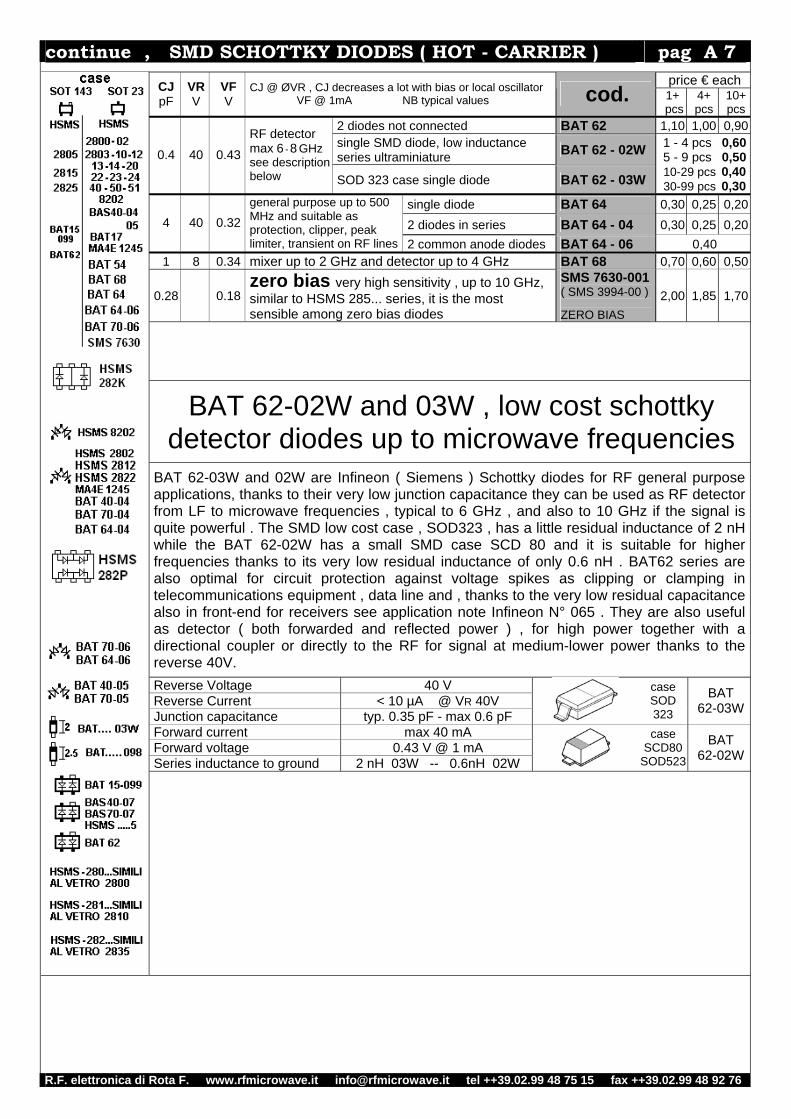
BAT 62-02W and 03W , low cost schottky detector diodes up to microwave frequencies
BAT 62-03W and 02W are Infineon ( Siemens ) Schottky diodes for RF general purpose applications, thanks to their very low junction capacitance they can be used as RF detector from LF to microwave frequencies , typical to 6 GHz , and also to 10 GHz if the signal is quite powerful . The SMD low cost case , SOD323 , has a little residual inductance of 2 nH while the BAT 62-02W has a small SMD case SCD 80 and it is suitable for higher frequencies thanks to its very low residual inductance of only 0.6 nH . BAT62 series are also optimal for circuit protection against voltage spikes as clipping or clamping in telecommunications equipment , data line and , thanks to the very low residual capacitance also in front-end for receivers see application note Infineon N° 065 . They are also useful as detector ( both forwarded and reflected power ) , for high power together with a directional coupler or directly to the RF for signal at medium-lower power thanks to the reverse 40V.
Reverse Voltage 40 V Reverse Current < 10 µA @ VR 40V Junction capacitance typ. 0.35 pF - max 0.6 pF
case SOD 323
BAT 62-03W
Forward current max 40 mA Forward voltage 0.43 V @ 1 mA Series inductance to ground 2 nH 03W -- 0.6nH 02W
case SCD80
SOD523
BAT 62-02W
R.F. elettronica di Rota F. www.rfmicrowave.it [email protected] tel ++39.02.99 48 75 15 fax ++39.02.99 48 92 76
continue , SMD SCHOTTKY DIODES ( HOT - CARRIER ) pag A 8
Beam lead - chip DIE for bonding or millimeter waves
ATTENTION : beam lead and die components have nearly microscopic size , in order to mount them you need to use particular techniques like bonding or silver glue , besides a microscope is needed .
CJ pF
VR V
VF V
CJ @ ØVR , CJ decreases a lot with bias or local oscillator VF @ 1mA NB typical values cod. price € each
1 - 10 pcs 0.05 4.5 0.68 GaAs, specified for 44 GHz 6.7dBNF, up to 200GHz see Dubus 2-94 HSCH - 9101 26,00
0.05 4.5 0.68 GaAs , double diode HSCH 9101 parallel pair in a single case for sub-harmonic mixer up to 100 GHz HSCH - 9251 37,00
0.1 4 0.35 up to 30 - 40 GHz, 7.5dBNF@ 26 GHz - Rs < 20 Ω Tss -54dBm @ 10 GHz with 10 µA bias
DMB 2856 ( = HSCH 5340 ) 15,00
0.08 4 GaAs specified for 35 GHz with NF 10 dB DC 1308 19,00 0.2 4 0.47 Pair connected in series with central tap, Tss -48dBm BAT 14-050 D 11,00 - 8,50
0.14 4 0.49 Pair connected in series with central tap up to 24 GHz BAT 14-090 D 16,00
0,1 4 0,50 single diode, it has the lowest residual capacitance of the BAT 14 family, for mixers and detectors up to 40 GHz , 7 dBNF @ 16 GHz OL 0dBm Rs 10 Ω , similar to chip ceramic BAT 14-124
BAT 14-110 S 16,00
0.14 4 0.3 low barrier as BAT14-090D high sensitivity Tss = -53dBm, up to 24 GHz BAT 15-090 D 22,00
finishing GaAs for millimeter frequencies MA4E 2037 on request
0.06 5 0,7 GaAs for millimeter frequencies MA4E 2039 on request 0.1 2 0.31 up to 40 GHz , mixer with 7.5 dBNF @ 16 GHz , Rs 18 Ω MA 40131 on request
0.1 3 0.41 ( = HSCH 5312 ) up to 30 - 40 GHz , beam strenght up to 10 g Very good mixer with average LO level MA 40133 15,00
0.14 6.5 0.2 high tangential sensitivity -56dBm (without bias) very good low barrier as detector diode for millimeter frequencies
= BAT 30 or DCC 2351-24
M2X4147
ZERO BIAS
1 pc = 10,00 50 pcs = 3,80
each
5 0.6 bridge quad, Cj from 0.05 to 0.25 pF, Macom 906 case MA 4E 400H-906 15,00
0.1 3 0.3 glass case Surmount type ( not beam lead ) , see more detailed informations on the previous pages in microwave diodes MA 4E 2502L on request
0.15 3 0.45 chip die, up to 26 GHz
1 15 chip die similar to 5082-2811 up to 3 GHz ,it is used as mixer in some HP spectrum analyzers
BAT 14-B 5082-0097 on request
0.1 5 0,52 Cj 0.07-0.12 pF , up to 100 GHz , Rs 9 Ω , Rd 18 Ω , Fco 253 GHz Aeroflex-Metelics MSS50-146-B10B MSS50-146 16,00
REPLACEMENTS for schottky diodes : BAR10 with 5082-2810 -- BAR 11 with 5082-2810 -- BAR 18 with HSMS-2840
BAR 28 with HP5082-2800 -- BAR 29 with HSMS-2820 -- BAR 43 with BAT 54 --- BAS 70 with HSMS-2840 BAS 125-05 with HSMS-2814 -- BAS 125-06 with HSMS-2813 -- BAS 125-07 with HSMS-2825 BAT 14-03W and BAT 14-098 with BAT 62-03W -- BAT 14-099 with HSMS-8202 or MA4E1245KB if connected in series or antiparallel -- BAT 16 glass case with SMD BAT62-03W -- BAT 17.... with HSMS 282.. with same configuration BAT 19 with 5082-2811 -- BAT 41 with BAT 46 -- BAT 47 with BAT 46 -- BAT 64 with HSMS-2840 BAT 64-04 with HSMS-2802 -- BAT 68 - ... eith HSMS-282... with same configuration
R.F. elettronica di Rota F. www.rfmicrowave.it [email protected] tel ++39.02.99 48 75 15 fax ++39.02.99 48 92 76
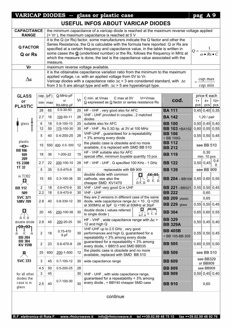
VARICAP DIODES -- glass or plastic case pag A 9
USEFUL INFOS ABOUT VARICAP DIODES
CAPACITANCE RANGE
the minimum capacitance of a varicap diode is reached at the maximum reverse voltage applied (= Vr ), the maximum capacitance is reached at 0 V
Q FACTOR
Q or Rs
it is the Q (or Rs) factor, some manufacturers indicate the Q factor and other the Series Resistance, the Q is calculable with the formula here reported. Q or Rs are specified at a certain frequency and capacitance value, in the table is written in some cases the Q (underlined number) or the Rs, follows the frequency in MHz at which the measure is done, the last is the capacitance value associated with the measure.
Vr maximum reverse voltage available.
∆c
it is the obtainable capacitance variation ratio from the minimum to the maximum applied voltage, i.e. with an applied voltage from 0V to Vr. Varicap diodes with a capacitance ratio ∆c < 3 are considered standard, with ∆c from 3 to 5 are abrupt type and with ∆c > 5 are hyperabrupt type.
continue
cap. (pF) Q-MHz-pF price € each or min max
RS-MHz-pF Vr C min. at Vmax C max at 0V Vr=Vmax
Q expressed as Q factor or series resistance Rs cod. 1+ pcs
4+ pcs
10+pcs
28 65 0.5-30-50 20 HF - VHF , very good also for AFC BA 111 0,45 0,40 0,35
2.7 16 100-50-11 28 VHF - UHF provided in couples , 2 matched diodes BA 142 1,20 / pair
6 18 0.8-100-10 25 suitable also for AFC BB 100 0,50 0,45 0,4012 50 175-100-30 30 HF - VHF , Rs 0.3Ω tip. at 3V at 100 MHz BB 103 =BA102 0,60 0,55 0,55
5 40 0.4-200-25 28 VHF-UHF , guaranteed for a repeatability < 3% among every diode
BB 106 = BB 109G 0,55 0,50 0,45
15 550 400- 0.5- 500 12 the plastic case is obsolete and no more available, it is replaced with SMD BB 510
BB 112 BB 212 see BB 510
18 36 1-200-22 15 HF - VHF suitable also for AFC special offer, minimum buyable quantity 10 pcs BB 119 0,30
min. 10 pcs
2.7 22 200-100-10 28 HF - VHF - UHF , Q specified 100 KHz - 1 GHz BB 122 0,50 0,45 0,40
5 35 0.5-470-9 30 replaceable with BB 909 BB 139 see BB 909
15 65 0.3-100-38 30 double diode with common cathode, see also the cheaper SMD KV1470
BB 204 = BB104 0,65 0,60 0,55
2 18 0.6-470-9 30 VHF - UHF very good Q in UHF BB 221 = BB521 0,55 0,50 0,452.2 18 0.9-470-9 30 VHF - UHF BB 222 0,60
BB 209 plastic 0,65 2.8 40 0.8-330-12 30
they are 2 versions in different case of the same diode, wide capacitance range Δc > 10 , Q =250 at 300MHz at 3pF Q =180 at 50MHz at 30pF BB 229 glass 0,55 0,50 0,45
20 45 200-100-38 30 double diode ( values referred to single diode )
BB 304 0,65 0,60 0,55
2.8 45 200-20-25 30 HF - VHF , wide capacitance range with Δc > 12 and high Q
BB 329 BB 329A 0,50 0,45 0,40
2 18 0.75-470 9 pF 30
VHF-UHF up to 2.5 GHz , very good performances and high Q, guaranteed for a repeatability < 3% among every diode
BB 405B
= BB 105-BB 205 0,55 0,50 0,45
2 23 0.6-470-9 28 guaranteed for a repeatability < 3% among every diode, = BB515 and SMD BB535 BB 505 0,60 0,55 0,50
25 600 200-1-500 12 the plastic case is obsolete and no more available, replaced with SMD BB 510 BB 509 see BB 510
3 45 0.7-100-12 30 wide capacitance range BB 609 see BB329 or BB909
4.5 50 0.5-200-25 28 BB 809 see BB909 3 45 30 BB 909 0,50 0,45 0,40
2.5 40
0.7-100-30 30
VHF - UHF , with wide capacitance range, guaranteed for a repeatability < 3% among every diode , = BBY40 cheaper SMD case BB 910 0,60
CRsQ
••=ω
1
min.max.
capcap
=
R.F. elettronica di Rota F. www.rfmicrowave.it [email protected] tel ++39.02.99 48 75 15 fax ++39.02.99 48 92 76
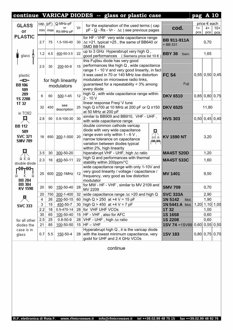
continue VARICAP DIODES -- glass or plastic case pag A 10
continue
cap. (pF) Q-MHz-pF price € each or
min max RS-MHz-pF Vr for the explanation of the used terms ( cap
pF - Q - Rs - Vr - ∆c ) see previous pages cod. 1+ pcs
4+ pcs
10+pcs
2.7 75 1.5-100-40 30 for HF - VHF very wide capacitance range ∆c >21, typical >25 , the same of BB640 or SMD BB164
BB 911-911A = BB 531 0,70
1.2 4.5 400-50-3.5 22 up to 3 GHz Hyperabrupt very high Q , good performances ( Siemens price list 10 € ) BBY 36 Siem. 1,65
2.5 30 200-50-9 15
for high linearity modulators
this Fujitsu diode has very good performances like high Q , wide capacitance range 1 - 10 V and very good linearity, in fact it was used in 70 or 140 MHz low distortion modulators on microwave radio links, guaranteed for a repeatability < 3% among every diode
FC 54 Fuji
0,55 0,50 0,45
6 60 500-1-45 12 high Q , with wide capacitance range within 2 - 10 V DKV 6510 0,85 0,80 0,75
32 450 see description 25
linear response Freq/ V tune high Q ≥700 at 10 MHz at 200 pF or Q ≥150 at 50 MHz at 200 pF
DKV 6525 11,80
2.8 50 0.9-100-30 30 similar to BB909 and BB910, VHF - UHF , with wide capacitance range HVS 303 0,50 0,45 0,40
18 650 300-1-500 20
double common cathode varicap diode with very wide capacitance range even only within 1 - 6 V , narrow tolerance on capacitance variation between diodes typical within 2%, high linearity
KV 1590 NT 3,20
3.5 30 300-50-20 hiperabrupt VHF - UHF, high ∆c ratio MA4ST 520D 1,20
2.3 16 450-50-11 22 high Q and performances with thermal stability within 200ppm/°C MA4ST 533C 1,60
25 600 200-1MHz 12
wide capacitance range with only 1-10V and very good linearity / voltage / capacitance / frequency, very good as low distortion modulator
MV 1401 9,50
20 90 150-50-40 28 for MW - HF - VHF , similar to MV 2109 and MV 2209 SMV 709 0,70
20 750 300-1-400 32 wide capacitance range ∆c >20 and high Q SVC 333A 2,90 4 26 250-50-15 60 high Q > 250 at +4 V = 15 pF 1N 5142 Mot. 1,90 3 15 450-50-7 30 high Q > 450 at +4 V = 7 pF 1N 5441 A Mot. 1,20 1,10 1,00
2.2 18 0.5-470-14 28 for VHF UHF VCOs 1T 32 1,00 30 65 100-50-40 15 HF - VHF , also for AFC 1S 1658 0,60 2.5 25 0.8-50-9 28 VHF - UHF , high ∆c ratio 1S 2208 0,60 21 85 100-50-50 15 HF – VHF 1SV 74 =1SV89 0,60 0,55 0,50
0.7 5.5 150-50-4 28
Hyperabrupt high Q , it is the varicap diode with the lowest minimum capacitance, very godd for UHF and 2.4 GHz VCOs
1SV 183 0,80 0,75 0,70
R.F. elettronica di Rota F. www.rfmicrowave.it [email protected] tel ++39.02.99 48 75 15 fax ++39.02.99 48 92 76
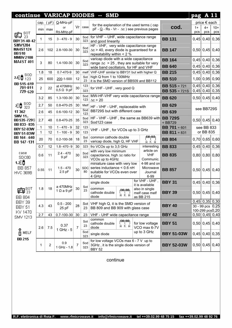
continue VARICAP DIODES -- SMD pag A 11
continue
cap. ( pF) Q-MHz-pF price € each or min max
RS-MHz-pF Vr case for the explanation of the used terms ( cap
pF - Q - Rs - Vr - ∆c ) see previous pages cod. 1+ pcs
4+ pcs
10+ pcs
1 15 3 - 470 - 9 30 Sod323
for VHF – UHF, wide capacitance range and good linearity BB 131 0,45 0,40 0,36
2.6 102 2.8-100-30 30 Sod 323
HF - VHF, very wide capacitance range ∆c > 40, every diode is guaranteed for a repeatability within < 2 %
BB 147 0,50 0,45 0,40
BB 164 0,45 0,40 0,363 80 1.4-100-30 30 Sod
323
varicap diode with a wide capacitance range ∆c > 25 , they are suitable for very wide band oscillators, for HF and VHF BB 640 0,45 0,40 0,36
1.8 18 0.7-470-9 30 melf VHF-UHF similar to BBY31 but with higher Q BB 215 0,45 0,40 0,3625 600 200-1-500 12 Sot
23 high Q from 1 to 100MHz it is the SMD version of BB509 and BB112 BB 510 1,00 0,95 0,90
123 BB 515 = 721 0,45 0,40 0,362 22 at 470MHz 0,5 Ω 9 pF 30
323 for VHF - UHF , very good Q
BB 535 = 721S 0,45 0,40 0,35
3.2 85 1.3-100-30 30 Sod 123
MW-HF-VHF very wide capacitance range∆c > 20 BB 620 0,50 0,45 0,40
2,7 50 0.8-470-25 30 Melf BB 629 2.6 45 0.6-100-12 30 Sod
123
HF - VHF - UHF, replaceable with BB729S but with different case BB 639
see BB729S
2,7 48 0.8-470-25 35 Sod 323
HF - VHF - UHF , the same as BB639 withSod123 case
BB 729S = BB729 0,50 0,45 0,40
1 10 1 - 470 - 9 32 123 BB 701 = 601 1 12 1 - 100 - 9 30 123
VHF - UHF , for VCOs up to 3 GHz BB 811 = 831 see BB 833 or BB 835
20 70 0.2-100-38 18 Sot 23
common cathode double varicap diode, high Q, HF VHF
BB 804 0,70 0,65 0,60
0.7 12 1.8 - 470 - 9 30 323 fro VCOs up to 3,5 GHz BB 833 0,45 0,40 0,36
0.6 11 2.4 - 470 9 pF 30 Sod
323
with very low minimum capacitance, high ∆c ratio for VCOs up to 4GHz
BB 835 0,80 0,80 0,80
0.55 11 1.5 - 470 2.5 pF 30 SDC
80
miniature case with very low series inductance < 0.6 nH suitable for VCOs even over 4 GHz
interesting article on
VHF Communic. 4-98 and onMicrowave
Journal 6-99
BB 857 0,50 0,45 0,40
single diode BBY 31 0,45 0,40 0,361.8 18 a 470MHz
1 Ω a 9 pF 30 Sot 23 common
cathode double diode
for VHF - UHF , it is available also in single melf case melf as BB 215
BBY 39 0,50 0,45 0,40
0,45 0,35 0,304.3 43 0.5 - 200
25 pF 28 Sot 23
VHF high Q, it is the SMD version of BB 809 and BB 909 with glass case BBY 40 30 - 99 pcs 0,25
100-299 pcs0,202.7 43 0.7-100-30 30 23 VHF - UHF wide capacitance range BBY 42 0,50 0,45 0,40
Sot 23
common cathode double diode
BBY 51 0,50 0,45 0,402.6 7.5 0.37
1 GHz - 5 7 Sod 323
single diode
for low voltage VCO max 6-7Vup to 3 GHz BBY 51-03W 0,45 0,40 0,35
1 2 0.9
1 GHz - 1.8 7 Sod 323
for low voltage VCOs max 6 - 7 V up to 3GHz , it is the single diode version of BBY 52
BBY 52-03W 0,50 0,45 0,40
R.F. elettronica di Rota F. www.rfmicrowave.it [email protected] tel ++39.02.99 48 75 15 fax ++39.02.99 48 92 76
continue VARICAP DIODES -- SMD pag A 12
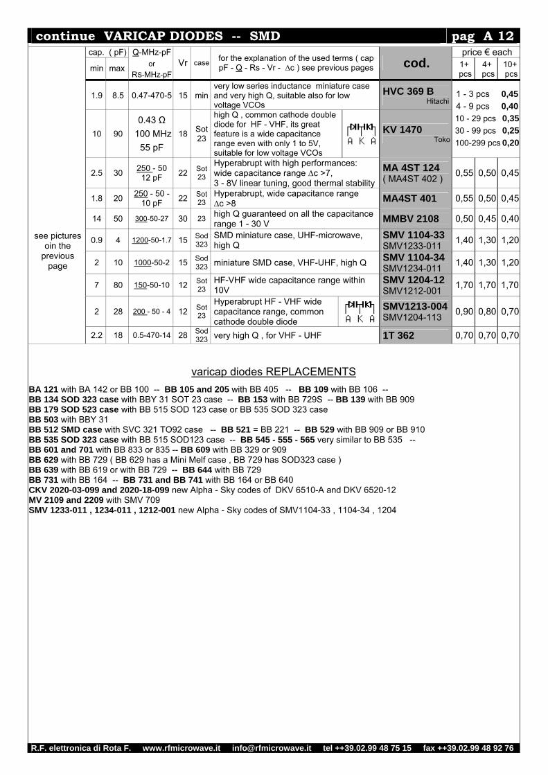
varicap diodes REPLACEMENTS
BA 121 with BA 142 or BB 100 -- BB 105 and 205 with BB 405 -- BB 109 with BB 106 -- BB 134 SOD 323 case with BBY 31 SOT 23 case -- BB 153 with BB 729S -- BB 139 with BB 909 BB 179 SOD 523 case with BB 515 SOD 123 case or BB 535 SOD 323 case BB 503 with BBY 31 BB 512 SMD case with SVC 321 TO92 case -- BB 521 = BB 221 -- BB 529 with BB 909 or BB 910 BB 535 SOD 323 case with BB 515 SOD123 case -- BB 545 - 555 - 565 very similar to BB 535 -- BB 601 and 701 with BB 833 or 835 -- BB 609 with BB 329 or 909 BB 629 with BB 729 ( BB 629 has a Mini Melf case , BB 729 has SOD323 case ) BB 639 with BB 619 or with BB 729 -- BB 644 with BB 729 BB 731 with BB 164 -- BB 731 and BB 741 with BB 164 or BB 640 CKV 2020-03-099 and 2020-18-099 new Alpha - Sky codes of DKV 6510-A and DKV 6520-12 MV 2109 and 2209 with SMV 709 SMV 1233-011 , 1234-011 , 1212-001 new Alpha - Sky codes of SMV1104-33 , 1104-34 , 1204
cap. ( pF) Q-MHz-pF price € each or min max
RS-MHz-pF Vr case for the explanation of the used terms ( cap
pF - Q - Rs - Vr - ∆c ) see previous pages cod. 1+ pcs
4+ pcs
10+ pcs
1.9 8.5 0.47-470-5 15 min very low series inductance miniature case and very high Q, suitable also for low voltage VCOs
HVC 369 B Hitachi
10 90 0.43 Ω
100 MHz
55 pF 18 Sot
23
high Q , common cathode double diode for HF - VHF, its great feature is a wide capacitance range even with only 1 to 5V, suitable for low voltage VCOs
KV 1470 Toko
1 - 3 pcs 0,45
4 - 9 pcs 0,40
10 - 29 pcs 0,35
30 - 99 pcs 0,25
100-299 pcs 0,20
2.5 30 250 - 50 12 pF 22 Sot
23
Hyperabrupt with high performances: wide capacitance range ∆c >7, 3 - 8V linear tuning, good thermal stability
MA 4ST 124 ( MA4ST 402 ) 0,55 0,50 0,45
1.8 20 250 - 50 - 10 pF 22 Sot
23 Hyperabrupt, wide capacitance range ∆c >8 MA4ST 401 0,55 0,50 0,45
14 50 300-50-27 30 23 high Q guaranteed on all the capacitance range 1 - 30 V MMBV 2108 0,50 0,45 0,40
0.9 4 1200-50-1.7 15 Sod 323
SMD miniature case, UHF-microwave, high Q
SMV 1104-33 SMV1233-011 1,40 1,30 1,20
2 10 1000-50-2 15 Sod323 miniature SMD case, VHF-UHF, high Q SMV 1104-34
SMV1234-011 1,40 1,30 1,20
7 80 150-50-10 12 Sot 23
HF-VHF wide capacitance range within 10V
SMV 1204-12 SMV1212-001 1,70 1,70 1,70
2 28 200 - 50 - 4 12 Sot 23
Hyperabrupt HF - VHF wide capacitance range, common cathode double diode
SMV1213-004 SMV1204-113 0,90 0,80 0,70
see pictures oin the
previous page
2.2 18 0.5-470-14 28 Sod323 very high Q , for VHF - UHF 1T 362 0,70 0,70 0,70
R.F. elettronica di Rota F. www.rfmicrowave.it [email protected] tel ++39.02.99 48 75 15 fax ++39.02.99 48 92 76
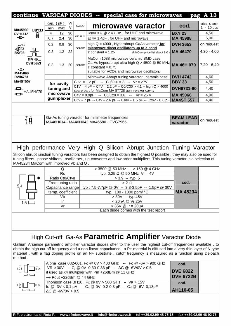
continue VARICAP DIODES -- special case for microwaves pag A 13
cap. ( pF ) min max
Vr V case microwave varactor cod. price € each
1 - 10 pcs
4 12 30 Rs=0.9 Ω @ 2.4 GHz , for UHF and microwave BXY 23 4,50 0.7 2.4 30
ceram at 4V 1.4pF , for UHF and microwave MA 45988 5,00
0.2 0.9 30 DVH 3653 on request
0.3 1.2 22 ceram
high Q = 4000 , Hyperabrupt GaAs varactor for microwave direct oscillators up to X band ϒ constant = 1.25 (MaCom price list about 9 € )
MA 46470 4,30 - 4,00
0.3 1.3 20 ceram
MaCom 1088 microwave ceramic SMD case, Ga-As hyperabrupt ultra high Q > 4500 @ 50 MHz ϒ constant = 0.75 suitable for VCOs and microwave oscillators
MA 46H 070 7,20 - 6,40
Microwave Abrupt tuning varactor , ceramic case DVH 4742 4,60 C0V = 1.2 pF -- C0/C20 = 3 -- Vr = 27V BBY 33 4,50 C1V = 4 pF -- C4V = 2.2 pF -- C0/C30 > 4.1 -- high Q > 4000 spare part for MaCom MA 87728 gunn-plexer cavity DVH6731-90 4,40
C4V = 0.9pF -- C0/C20 = 3.6 -- Vr = 25 V MA 45066 4,90
for cavity tuning and microwave gunnplexer C0V = 7 pF -- C4V = 2.6 pF -- C10V = 1.5 pF -- C20V = 0.8 pF MA4ST 557 4,40
Ga-As tuning varactor for millimeter frequencies MA46H014 - MA46H042 MA46580 - CVG7965
BEAM LEADvaractor on request
High performance Very High Q Silicon Abrupt Junction Tuning Varactor
Silicon abrupt junction tuning varactors has been designed to obtain the highest Q possible , they may also be used for tuning filters , phase shifters , oscillators , up-converter and low order multipliers. This tuning varactor is a selection of MA45234 MaCom with improved Vb and Q .
Q > 3500 @ 50 MHz -- > 150 @ 4 GHz Rs typ. 0,25 Ω @ 50 MHz Vr = 4V
Ratio Ct0/CtVB > 3.9 -- typ. 5 Freq tuning ratio > 2 :1
Capacitance range typ : 7.5-7.7pF @ 0V -- 3.3-3.5pF -- 1.5pF @ 30V temp. coefficient typ. 100 - 1000 ppm/ °C
Vb > 30V -- typ 45V Ir < 20nA @ Vr 25V Vr > 35V @ Ir = 20µA
cod. MA 45234
Each diode comes with the test report
High Cut-off Ga-As Parametric Amplifier Varactor Diode
Gallium Arsenide parametric amplifier varactor diodes offer to the user the highest cut-off frequencies available , to obtain the high cut-off frequency and a non-linear capacitance , a P+ material is diffused into a very thin layer of N type material , with a flag doping profile on an N+ substrate , cutoff frequency is measured as a function using Deloach method .
Alpha case 082-001, Fc @ 0V > 400 GHz -- Fc @ -6V > 900 GHz VR ≥ 30V -- Cj @ 0V 0.30-0.33 pF -- ΔC @ -6V/0V > 0.5 if used as x4 multiplier with Pin +26dBm @ 11 GHz → Pout +22dBm @ 44 GHz
cod.
DVE 6822 DVE 6722B
Thomson case BH10 , FC @ 0V > 500 GHz -- VR > 15V IR @ -3V < 0,1 µA -- CJ @ 0V 0.2-0.3 pF -- CJ @ -6V 0,13pF ΔC @ -6V/0V > 0.5
cod.
AH110-05
R.F. elettronica di Rota F. www.rfmicrowave.it [email protected] tel ++39.02.99 48 75 15 fax ++39.02.99 48 92 76
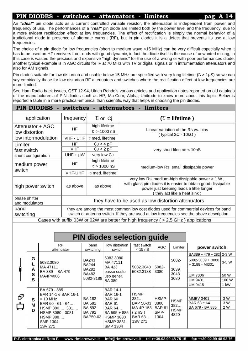
PIN DIODES - switches - attenuators - limiters pag A 14
An “ideal” pin diode acts as a current controlled variable resistor, the attenuation is independent from power and frequency of use. The performances of a "real" pin diode are limited both by the power level and the frequency, due to a more evident rectification effect at low frequencies. The effect of rectification is simply the normal behavior of a tradictional diode in presence of alternate current (RF), but in pin diodes it is a defect that prevents its use at low frequencies.
The choice of a pin diode for low frequencies (short to medium wave <15 MHz) can be very difficult especially when it has to be used on HF receivers front-ends with good dynamic, in fact the diode itself is the cause of unwanted mixing, in this case is wasted the precious and expensive "high dynamic" for the use of a wrong or with poor performances diode, another typical example is in AGC circuits for IF at 70 MHz with TV or digital signals or in intrumentation attenuators and also for AM signals.
Pin diodes suitable for low distortion and usable below 15 MHz are specified with very long lifetime (Շ > 1μS) so we can say empirically those for low distortion RF attenuators and switches where the rectification effect at low frequencies are more limited.
See Ham Radio back issues, QST 12-94, Ulrich Rohde’s various articles and application notes reported on old catalogs of the manufacturers of PIN diodes such as HP, Ma-Com, Alpha, Unitrode to know more about this topic. Below is reported a table in a more practical-empirical than scientific way that helps in choosing the pin diodes.
PIN DIODES - switches - attenuators - limiters
application frequency Շ or Cj (Շ = lifetime )
HF high lifetime
Շ > 1000 nS Attenuator + AGC low distortion low intermodulation VHF - UHF Շ med. lifetime
Linear variation of the RS vs. bias ( typical 3Ω - 10kΩ )
HF CJ < 4 pF VHF CJ < 2 pF
Limiter fast switch shunt configuration UHF + µW very low CJ
very short lifetime < 10nS
HF high lifetime Շ > 1000 nS medium power
switch VHF-UHF Շ med. lifetime medium-low RS, small dissipable power
high power switch as above as above
very low RS, medium-high dissipable power > 1 W , with glass pin diodes it is easier to obtain good dissipable
power just keeping leads a little longer ( they act like a heat sink )
phase shifter and modulators they have to be used as low distortion attenuators
band switching
they are among the most common low cost diodes used for commercial devices for band switch or antenna switch. If they are used at low frequencies see the above description.
Cases with suffix 03W or 02W are better for high frequency ( > 2,5 GHz ) applications
PIN diodes selection guide
RF attenuator
band switching
low distortion switch
fast switch< 15 nS AGC Limiter power switch
BA389 + 479 + 282 2-3 W 5082-3039 + 3080 + 3188 - MI301 3-5 W
UM 7006 50 W UM 9401 100 W
G L A S S
5082.3080 MA 47111 BA 389 BA 479 MA4P4006
BA243 BA244 BA282 BA482 5082-3188
5082.3080 MA 47111 BA 423 basso costo uso gener. BA 389
5082.3043 5082.3188
5082- 3080
5082- 3039 3043 3080
UM 9415 1 kW MMBV 3401 3 W BAR 63 e 64 3 W BA 679 - BA 885 2 W
S M D
BA 679 - 885 BAR 14-1 e BAR 16-1 > 10 MHz BAR 60 - 61 - 64…. HSMP 380…. 381…. HSMP 3080 - 3081 HSMP 388…. SMP 1304 1SV 271
BA 182 BA 582 BA 592 BA 792 BAP50-03
BAR 14-1 BAR 16-1 BAR 60 BAR 61 BAR 64… BA 595 + 885 HSMP 3880 HSMP 3881 SMP 1304
HSMP 382… BAP 50-03MA 4P 153( 2 nS ) BAR 63.... 1SV 271
HSMP-3800 BAR 61SMP- 1304
HSMP 382… HSMP 4820
R.F. elettronica di Rota F. www.rfmicrowave.it [email protected] tel ++39.02.99 48 75 15 fax ++39.02.99 48 92 76
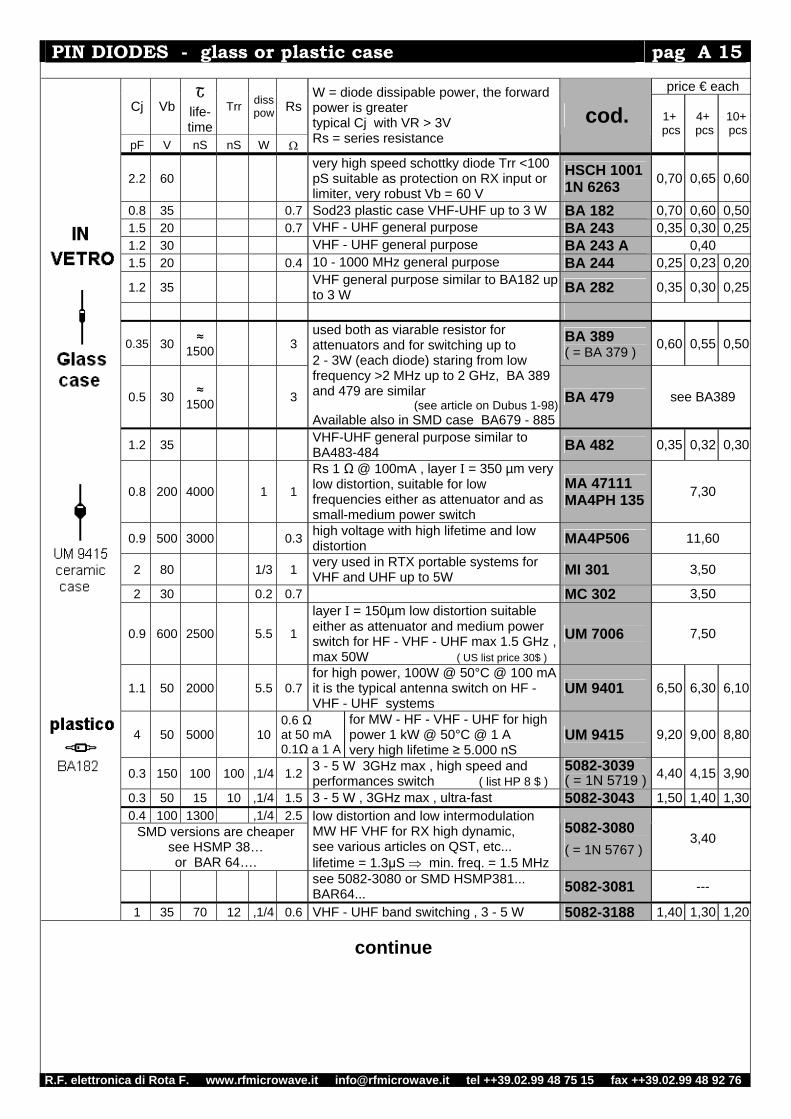
PIN DIODES - glass or plastic case pag A 15
continue
price € each Cj Vb
Շ
life- time
Trr diss pow Rs
pF V nS nS W Ω
W = diode dissipable power, the forward power is greater typical Cj with VR > 3V Rs = series resistance
cod. 1+ pcs
4+ pcs
10+ pcs
2.2 60
very high speed schottky diode Trr <100 pS suitable as protection on RX input or limiter, very robust Vb = 60 V
HSCH 1001 1N 6263 0,70 0,65 0,60
0.8 35 0.7 Sod23 plastic case VHF-UHF up to 3 W BA 182 0,70 0,60 0,501.5 20 0.7 VHF - UHF general purpose BA 243 0,35 0,30 0,251.2 30 VHF - UHF general purpose BA 243 A 0,40 1.5 20 0.4 10 - 1000 MHz general purpose BA 244 0,25 0,23 0,20
1.2 35 VHF general purpose similar to BA182 up to 3 W BA 282 0,35 0,30 0,25
0.35 30 ≈ 1500
3 BA 389
( = BA 379 ) 0,60 0,55 0,50
0.5 30 ≈ 1500
3
used both as viarable resistor for attenuators and for switching up to 2 - 3W (each diode) staring from low frequency >2 MHz up to 2 GHz, BA 389 and 479 are similar
(see article on Dubus 1-98)Available also in SMD case BA679 - 885
BA 479 see BA389
1.2 35 VHF-UHF general purpose similar to BA483-484 BA 482 0,35 0,32 0,30
0.8 200 4000 1 1
Rs 1 Ω @ 100mA , layer I = 350 µm very low distortion, suitable for low frequencies either as attenuator and as small-medium power switch
MA 47111 MA4PH 135 7,30
0.9 500 3000 0.3 high voltage with high lifetime and low distortion MA4P506 11,60
2 80 1/3 1 very used in RTX portable systems for VHF and UHF up to 5W MI 301 3,50
2 30 0.2 0.7 MC 302 3,50
0.9 600 2500 5.5 1
layer I = 150µm low distortion suitable either as attenuator and medium power switch for HF - VHF - UHF max 1.5 GHz , max 50W ( US list price 30$ )
UM 7006 7,50
1.1 50 2000 5.5 0.7 for high power, 100W @ 50°C @ 100 mAit is the typical antenna switch on HF - VHF - UHF systems
UM 9401 6,50 6,30 6,10
4 50 5000 10 0.6 Ω at 50 mA 0.1Ω a 1 A
for MW - HF - VHF - UHF for high power 1 kW @ 50°C @ 1 A very high lifetime ≥ 5.000 nS
UM 9415 9,20 9,00 8,80
0.3 150 100 100 ,1/4 1.2 3 - 5 W 3GHz max , high speed and performances switch ( list HP 8 $ )
5082-3039 ( = 1N 5719 ) 4,40 4,15 3,90
0.3 50 15 10 ,1/4 1.5 3 - 5 W , 3GHz max , ultra-fast 5082-3043 1,50 1,40 1,300.4 100 1300 ,1/4 2.5
SMD versions are cheaper see HSMP 38… or BAR 64….
low distortion and low intermodulation MW HF VHF for RX high dynamic, see various articles on QST, etc... lifetime = 1.3μS ⇒ min. freq. = 1.5 MHz
5082-3080
( = 1N 5767 ) 3,40
see 5082-3080 or SMD HSMP381... BAR64... 5082-3081 ---
1 35 70 12 ,1/4 0.6 VHF - UHF band switching , 3 - 5 W 5082-3188 1,40 1,30 1,20
R.F. elettronica di Rota F. www.rfmicrowave.it [email protected] tel ++39.02.99 48 75 15 fax ++39.02.99 48 92 76
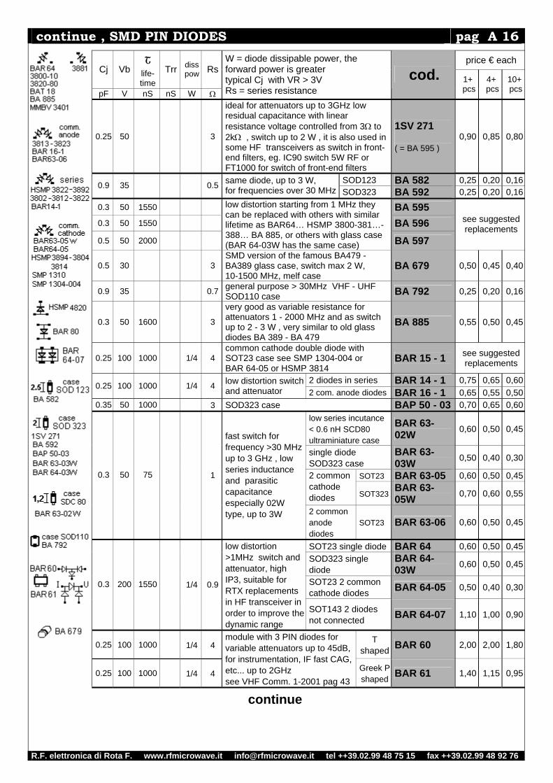
continue , SMD PIN DIODES pag A 16
continue
price € each Cj Vb
Շ life- time
Trr diss pow Rs
pF V nS nS W Ω
W = diode dissipable power, the forward power is greater typical Cj with VR > 3V Rs = series resistance
cod. 1+ pcs
4+ pcs
10+ pcs
0.25 50 3
ideal for attenuators up to 3GHz low residual capacitance with linear resistance voltage controlled from 3Ω to 2kΩ , switch up to 2 W , it is also used in some HF transceivers as switch in front-end filters, eg. IC90 switch 5W RF or FT1000 for switch of front-end filters
1SV 271 ( = BA 595 )
0,90 0,85 0,80
SOD123 BA 582 0,25 0,20 0,160.9 35 0.5 same diode, up to 3 W, for frequencies over 30 MHz SOD323 BA 592 0,25 0,20 0,16
0.3 50 1550 BA 595 0.3 50 1550 BA 596 0.5 50 2000
low distortion starting from 1 MHz they can be replaced with others with similar lifetime as BAR64… HSMP 3800-381…-388… BA 885, or others with glass case (BAR 64-03W has the same case) BA 597
see suggested replacements
0.5 30 3 SMD version of the famous BA479 - BA389 glass case, switch max 2 W, 10-1500 MHz, melf case
BA 679 0,50 0,45 0,40
0.9 35 0.7 general purpose > 30MHz VHF - UHF SOD110 case BA 792 0,25 0,20 0,16
0.3 50 1600 3
very good as variable resistance for attenuators 1 - 2000 MHz and as switch up to 2 - 3 W , very similar to old glass diodes BA 389 - BA 479
BA 885 0,55 0,50 0,45
0.25 100 1000 1/4 4 common cathode double diode with SOT23 case see SMP 1304-004 or BAR 64-05 or HSMP 3814
BAR 15 - 1 see suggested replacements
2 diodes in series BAR 14 - 1 0,75 0,65 0,600.25 100 1000 1/4 4 low distortion switch and attenuator 2 com. anode diodes BAR 16 - 1 0,65 0,55 0,50
0.35 50 1000 3 SOD323 case BAP 50 - 03 0,70 0,65 0,60low series incutance < 0.6 nH SCD80 ultraminiature case
BAR 63-02W 0,60 0,50 0,45
single diode SOD323 case
BAR 63-03W 0,50 0,40 0,30
SOT23 BAR 63-05 0,60 0,50 0,452 common cathode diodes SOT323
BAR 63-05W 0,70 0,60 0,55
0.3 50 75 1
fast switch for frequency >30 MHz up to 3 GHz , low series inductance and parasitic capacitance especially 02W type, up to 3W 2 common
anode diodes
SOT23 BAR 63-06 0,60 0,50 0,45
SOT23 single diode BAR 64 0,60 0,50 0,45SOD323 single diode
BAR 64-03W 0,60 0,50 0,45
SOT23 2 common cathode diodes BAR 64-05 0,50 0,40 0,300.3 200 1550 1/4 0.9
low distortion >1MHz switch and attenuator, high IP3, suitable for RTX replacements in HF transceiver in order to improve the dynamic range
SOT143 2 diodes not connected BAR 64-07 1,10 1,00 0,90
0.25 100 1000 1/4 4 T
shaped BAR 60 2,00 2,00 1,80
0.25 100 1000 1/4 4
module with 3 PIN diodes for variable attenuators up to 45dB, for instrumentation, IF fast CAG, etc... up to 2GHz see VHF Comm. 1-2001 pag 43
Greek P shaped BAR 61 1,40 1,15 0,95
R.F. elettronica di Rota F. www.rfmicrowave.it [email protected] tel ++39.02.99 48 75 15 fax ++39.02.99 48 92 76
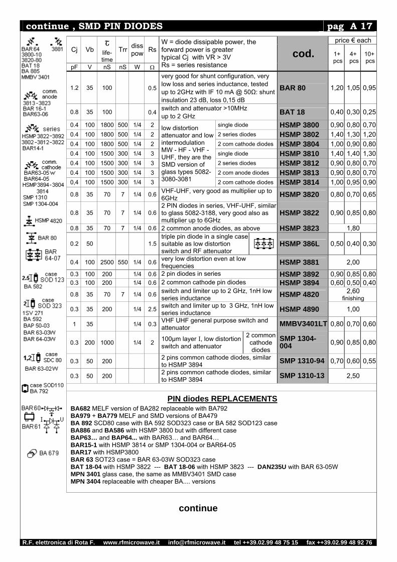
continue , SMD PIN DIODES pag A 17
continue
price € each Cj Vb
Շ life- time
Trr diss pow Rs
pF V nS nS W Ω
W = diode dissipable power, the forward power is greater typical Cj with VR > 3V Rs = series resistance
cod. 1+ pcs
4+ pcs
10+ pcs
1.2 35 100
0.5
very good for shunt configuration, very low loss and series inductance, tested up to 2GHz with IF 10 mA @ 50Ω: shunt insulation 23 dB, loss 0,15 dB
BAR 80 1,20 1,05 0,95
0.8 35 100 0.4
switch and attenuator >10MHz up to 2 GHz BAT 18 0,40 0,30 0,25
0.4 100 1800 500 1/4 2 single diode HSMP 3800 0,90 0,80 0,700.4 100 1800 500 1/4 2 2 series diodes HSMP 3802 1,40 1,30 1,200.4 100 1800 500 1/4 2 2 com cathode diodes HSMP 3804 1,00 0,90 0,800.4 100 1500 300 1/4 3 single diode HSMP 3810 1,40 1,40 1,300.4 100 1500 300 1/4 3 2 series diodes HSMP 3812 0,90 0,80 0,700.4 100 1500 300 1/4 3 2 com anode diodes HSMP 3813 0,90 0,80 0,700,4 100 1500 300 1/4 3
low distortion attenuator and low intermodulation MW - HF - VHF - UHF, they are the SMD version of glass types 5082-3080-3081 2 com cathode diodes HSMP 3814 1,00 0,95 0,90
0.8 35 70 7 1/4 0.6 VHF-UHF, very good as multiplier up to 6GHz HSMP 3820 0,80 0,70 0,65
0.8 35 70 7 1/4 0.6 2 PIN diodes in series, VHF-UHF, similar to glass 5082-3188, very good also as multiplier up to 6GHz
HSMP 3822 0,90 0,85 0,80
0.8 35 70 7 1/4 0.6 2 common anode diodes, as above HSMP 3823 1,80
0.2 50 1.5 triple pin diode in a single case suitable as low distortion switch and RF attenuator
HSMP 386L 0,50 0,40 0,30
0.4 100 2500 550 1/4 0.6 very low distortion even at low frequencies HSMP 3881 2,00
0.3 100 200 1/4 0.6 2 pin diodes in series HSMP 3892 0,90 0,85 0,800.3 100 200 1/4 0.6 2 common cathode pin diodes HSMP 3894 0,60 0,50 0,40
0.8 35 70 7 1/4 0.6 switch and limiter up to 2 GHz, 1nH low series inductance HSMP 4820 2,60
finishing
0.3 35 200 1/4 2.5 switch and limiter up to 3 GHz, 1nH low series inductance HSMP 4890 1,00
1 35 1/4 0.3 VHF UHF general purpose switch and attenuator MMBV3401LT 0,80 0,70 0,60
0.3 200 1000 1/4 2 100µm layer I, low distortion switch and attenuator
2 common cathode diodes
SMP 1304-004 0,90 0,85 0,80
0.3 50 200 2 pins common cathode diodes, similar to HSMP 3894 SMP 1310-94 0,70 0,60 0,55
0.3 50 200 2 pins common cathode diodes, similar to HSMP 3894 SMP 1310-13 2,50
PIN diodes REPLACEMENTS
BA682 MELF version of BA282 replaceable with BA792 BA979 + BA779 MELF and SMD versions of BA479 BA 892 SCD80 case with BA 592 SOD323 case or BA 582 SOD123 case BA886 and BA586 with HSMP 3800 but with different case BAP63… and BAP64... with BAR63… and BAR64… BAR15-1 with HSMP 3814 or SMP 1304-004 or BAR64-05 BAR17 with HSMP3800 BAR 63 SOT23 case = BAR 63-03W SOD323 case BAT 18-04 with HSMP 3822 --- BAT 18-06 with HSMP 3823 --- DAN235U with BAR 63-05W MPN 3401 glass case, the same as MMBV3401 SMD case MPN 3404 replaceable with cheaper BA.... versions
R.F. elettronica di Rota F. www.rfmicrowave.it [email protected] tel ++39.02.99 48 75 15 fax ++39.02.99 48 92 76
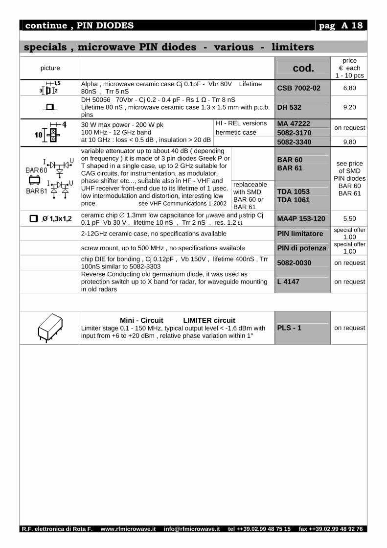
continue , PIN DIODES pag A 18 specials , microwave PIN diodes - various - limiters
picture cod. price
€ each 1 - 10 pcs
Alpha , microwave ceramic case Cj 0.1pF - Vbr 80V Lifetime 80nS , Trr 5 nS CSB 7002-02 6,80
DH 50056 70Vbr - Cj 0.2 - 0.4 pF - Rs 1 Ω - Trr 8 nS Lifetime 80 nS , microwave ceramic case 1.3 x 1.5 mm with p.c.b. pins
DH 532 9,20
HI - REL versions MA 47222 hermetic case 5082-3170
on request
30 W max power - 200 W pk 100 MHz - 12 GHz band at 10 GHz : loss < 0.5 dB , insulation > 20 dB 5082-3340 9,80
BAR 60 BAR 61
variable attenuator up to about 40 dB ( depending on frequency ) it is made of 3 pin diodes Greek P or T shaped in a single case, up to 2 GHz suitable for CAG circuits, for instrumentation, as modulator, phase shifter etc..., suitable also in HF - VHF and UHF receiver front-end due to its lifetime of 1 μsec. low intermodulation and distortion, interesting low price. see VHF Communications 1-2002
replaceable with SMD BAR 60 or BAR 61
TDA 1053 TDA 1061
see price of SMD
PIN diodesBAR 60 BAR 61
ceramic chip ∅ 1.3mm low capacitance for μwave and μstrip Cj 0.1 pF Vb 30 V , lifetime 10 nS , Trr 2 nS , res. 1.2 Ω MA4P 153-120 5,50
2-12GHz ceramic case, no specifications available PIN limitatore special offer 1.00
screw mount, up to 500 MHz , no specifications available PIN di potenza special offer 1,00
chip DIE for bonding , Cj 0.12pF , Vb 150V , lifetime 400nS , Trr 100nS similar to 5082-3303 5082-0030 on request
Reverse Conducting old germanium diode, it was used as protection switch up to X band for radar, for waveguide mounting in old radars
L 4147 on request
Mini - Circuit LIMITER circuit Limiter stage 0,1 - 150 MHz, typical output level < -1,6 dBm with input from +6 to +20 dBm , relative phase variation within 1°
PLS - 1 on request
R.F. elettronica di Rota F. www.rfmicrowave.it [email protected] tel ++39.02.99 48 75 15 fax ++39.02.99 48 92 76
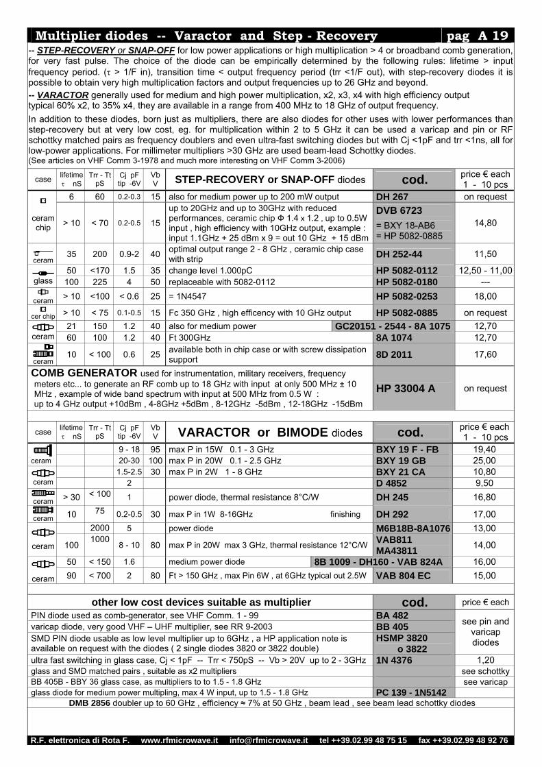
Multiplier diodes -- Varactor and Step - Recovery pag A 19
-- STEP-RECOVERY or SNAP-OFF for low power applications or high multiplication > 4 or broadband comb generation, for very fast pulse. The choice of the diode can be empirically determined by the following rules: lifetime > input frequency period. (τ > 1/F in), transition time < output frequency period (trr <1/F out), with step-recovery diodes it is possible to obtain very high multiplication factors and output frequencies up to 26 GHz and beyond.
-- VARACTOR generally used for medium and high power multiplication, x2, x3, x4 with high efficiency output typical 60% x2, to 35% x4, they are available in a range from 400 MHz to 18 GHz of output frequency.
In addition to these diodes, born just as multipliers, there are also diodes for other uses with lower performances than step-recovery but at very low cost, eg. for multiplication within 2 to 5 GHz it can be used a varicap and pin or RF schottky matched pairs as frequency doublers and even ultra-fast switching diodes but with Cj <1pF and trr <1ns, all for low-power applications. For millimeter multipliers >30 GHz are used beam-lead Schottky diodes. (See articles on VHF Comm 3-1978 and much more interesting on VHF Comm 3-2006)
case lifetime τ nS
Trr - Tt pS
Cj pF tip -6V
Vb V STEP-RECOVERY or SNAP-OFF diodes cod. price € each
1 - 10 pcs 6 60 0.2-0.3 15 also for medium power up to 200 mW output DH 267 on request
ceram chip
> 10 < 70 0.2-0.5 15
up to 20GHz and up to 30GHz with reduced performances, ceramic chip Ф 1.4 x 1.2 , up to 0.5W input , high efficiency with 10GHz output, example : input 1.1GHz + 25 dBm x 9 = out 10 GHz + 15 dBm
DVB 6723
= BXY 18-AB6 = HP 5082-0885
14,80
ceram
35 200 0.9-2 40 optimal output range 2 - 8 GHz , ceramic chip case with strip DH 252-44 11,50
50 <170 1.5 35 change level 1.000pC HP 5082-0112 12,50 - 11,00 glass 100 225 4 50 replaceable with 5082-0112 HP 5082-0180 ---
ceram > 10 <100 < 0.6 25 = 1N4547 HP 5082-0253 18,00
cer chip > 10 < 75 0.1-0.5 15 Fc 350 GHz , high efficency with 10 GHz output HP 5082-0885 on request
21 150 1.2 40 also for medium power GC20151 - 2544 - 8A 1075 12,70 ceram 60 100 1.2 40 Ft 300GHz 8A 1074 12,70
ceram
10 < 100 0.6 25 available both in chip case or with screw dissipation support 8D 2011 17,60
COMB GENERATOR used for instrumentation, military receivers, frequency meters etc... to generate an RF comb up to 18 GHz with input at only 500 MHz ± 10 MHz , example of wide band spectrum with input at 500 MHz from 0.5 W :
up to 4 GHz output +10dBm , 4-8GHz +5dBm , 8-12GHz -5dBm , 12-18GHz -15dBm
HP 33004 A on request
case lifetime τ nS
Trr - Tt pS
Cj pF tip -6V
Vb V VARACTOR or BIMODE diodes cod. price € each
1 - 10 pcs 9 - 18 95 max P in 15W 0.1 - 3 GHz BXY 19 F - FB 19,40
ceram 20-30 100 max P in 20W 0.1 - 2.5 GHz BXY 19 GB 25,00 1.5-2.5 30 max P in 2W 1 - 8 GHz BXY 21 CA 10,80
ceram 2 D 4852 9,50
ceram > 30 < 100 1 power diode, thermal resistance 8°C/W DH 245 16,80
ceram 10 75 0.2-0.5 30 max P in 1W 8-16GHz finishing DH 292 17,00 2000 5 power diode M6B18B-8A1076 13,00
ceram 100 1000
8 - 10 80 max P in 20W max 3 GHz, thermal resistance 12°C/W VAB811 MA43811 14,00
50 < 150 1.6 medium power diode 8B 1009 - DH160 - VAB 824A 16,00
ceram 90 < 700 2 80 Ft > 150 GHz , max Pin 6W , at 6GHz typical out 2.5W VAB 804 EC 15,00
other low cost devices suitable as multiplier cod. price € each PIN diode used as comb-generator, see VHF Comm. 1 - 99 BA 482 varicap diode, very good VHF – UHF multiplier, see RR 9-2003 BB 405 SMD PIN diode usable as low level multiplier up to 6GHz , a HP application note is available on request with the diodes ( 2 single diodes 3820 or 3822 double)
HSMP 3820 o 3822
see pin and varicap diodes
ultra fast switching in glass case, Cj < 1pF -- Trr < 750pS -- Vb > 20V up to 2 - 3GHz 1N 4376 1,20 glass and SMD matched pairs , suitable as x2 multipliers see schottkyBB 405B - BBY 36 glass case, as multipliers to to 1.5 - 1.8 GHz see varicap glass diode for medium power multipling, max 4 W input, up to 1.5 - 1.8 GHz PC 139 - 1N5142
DMB 2856 doubler up to 60 GHz , efficiency ≈ 7% at 50 GHz , beam lead , see beam lead schottky diodes
R.F. elettronica di Rota F. www.rfmicrowave.it [email protected] tel ++39.02.99 48 75 15 fax ++39.02.99 48 92 76
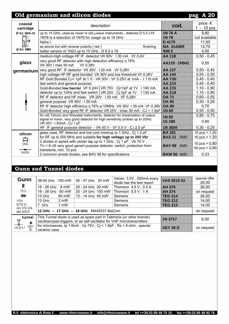
Old germanium and silicon diodes pag A 20
coaxial cartridge
description cod. price € 1 - 10 pcs
up to 15 GHz, used as mixer in old μwave instruments - detector D 5.5 x19 1N 76 A 9,80 1N78 is a selection of 1N76 for usage up to 18 GHz 1N 78 not availableAlpha I. D 4170 11,60 as above but with reverse polarity ( red ) finishing MA 41436R 12,70 better version of 1N23 up to 15 GHz , D 8.5 x 19 SIM 2 4,00
glass
germanium
medium-high voltage HF IF detector VR 90V I 30 mA VF 0,4V AA 118 0,50 - 0,45 very good RF detector with high detection efficiency ŋ 76% VR 30V I max 35 mA VF 0,38V AA119 - 1N541 0,55
very good RF IF detector VR 30V I 20 mA VF 0,28V AA 137 0,50 - 0,45 high voltage HF RF gold bonded VR 90V and low threshold VF 0,26V AA 144 0,55 - 0,50 RF Gold Bonded CJ< 1pF at 1 V - VR 30V - VF 0.25V at 1mA - I 110 mA AA Y30 0,45 - 0,40 fast switch and general purpose AA Z10 0,45 - 0,40 Gold-Bonded low barrier VF 0.24V detector up to 1GHz and fast switch
VR 75V Cj<1pF at 1V I 140 mA AA Z15 1,10 - 0,90 VR 20V Cj 2pF at 1V I 130 mA AA Z18 1,10 - 0,90
RF IF detector and HF mixer VR 20V I 50 mA VF 0,28V OA 73 0,60 - 0,55 general purpose VR 90V - I 50 mA OA 95 0,30 - 0,26 RF IF detector high efficiency ŋ 76% a 10MHz VR 30V I 35 mA VF 0,38V OA 99 0,70 Gold-Bonded very good RF IF detector VR 25V - Imax 30 mA - CJ < 1,5pF 1N 60 0,55 - 0,50 for old Telonic and Wavetek instruments, detector for linearization of output signal or mixer, very good detector for high sensitivity probes up to 2GHz VR 35V - I 50mA - CJ 1 pF
1N 82 1S 188
0,85 - 0,75 0,90
HF IF general purpose detector - VR 50 V - VF 0,5 V - CJ 2,5 pF 1N 3600 0,30 - 0,25
silicon
glass case, RF detector and low cost mixerup to 1 GHz , Cj 1.2 pF BA 281 10 pcs = 1,20for RF up to 500 MHz and suitable for high voltage up to 200 Vbr BAS 21 SMD 10 pcs = 1,202 diodes in series with center tap up to 1 GHz , Cj 1 pF , Vb 70 V , Trr < 6 nS very good generl purpose detector, switch, protection from transients, min. 10 pcs
BAV 99 SMD 10 pcs = 0,8050 pcs = 2,80
2 common anode diodes, see BAV 99 for specifications BAW 56 SMD 0,23 Gunn and Tunnel diodes
Gunn
38-40 GHz 100 mW 30 - 47 GHz 30 mW Varian 5.5V , 500mA every diode has the test report VAS 9210 IU special offer
26,00 18 - 26 GHz 8 mW 20 - 24 GHz 20 mW Thomson 4,5 V , 0.5 A AH 370 26,00 18 - 26 GHz 60 mW 20 - 24 GHz 150 mW Thomson 5,5 V , 1 A AH 374 on request 13 GHz 60 mW 12 - 14 GHz 40 mW Siemens TEG 214 26,00 13 GHz 2 mW Siemens TEG 212 14,00 7 GHz 1 mW Siemens TEG 213 14,00 12 GHz -- 17 GHz -- 18 GHz MA49337 MaCom on request
This Tunnel diode is used as spare part in Tektronix (or other brands) oscilloscopes triggers, or as self oscillator for VHF microtransmitters 1N 3717 9,30 for microwaves, Ip 1.6mA , Vp 75V , Cj < 1.8pF , Rs < 8 ohm , special ceramic case AEY 30 D on request
R.F. elettronica di Rota F. www.rfmicrowave.it [email protected] tel ++39.02.99 48 75 15 fax ++39.02.99 48 92 76
NOISE SOURCE diodes pag A 21
All the materials generate noise and the noise is proportional to its temperature starting from 0°K (-273°C). The noise depends on the chaotic movements of the electrons, the thermal noise is known as white noise (from optical physics) as it fills the whole spectrum. From an electronics point of view the noise causes big limitations to our devices for example amplifiers, instruments, radars, receivers, electro-medical, etc… A very simple example is the sensitivity limitation of receivers caused by the noise. Although the noise causes problems and limitations, it will be explained how in some cases, if it is artificially generated, it can even improve our electronic devices (see dithering) or help to do some tests, a calibrated noise source is a very important tool in our labs. NOISE GENERATORS . The first noise generators used noble gas such as Argon with 15.3dBENR, Neon with 18.5dBENR, Helium with 21dBENR and were born in order to test the first radar systems in the 1940s. Another method to generate noise is to use hot and cold resistors, mainly used in research labs with very high precision, this technique due to its complexity is used only in physic laboratories or in calibration centers. Today the most used noise generators are special diodes, noise diodes. A reverse polarized diode until it reaches the avalanche effect is an example of noise generator (see Zener diodes). Unlike Zener diodes, the noise diodes are doped and developed to cover a wider band (low Cj) with an output level really flat and more stable.
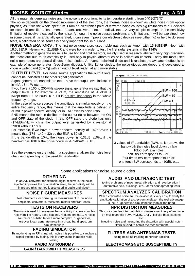
OUTPUT LEVEL For noise source applications the output level cannot be indicated as for other signal generators. Signal generators, transmitters etc… have the output level indication in mV, dBm, W etc…. If you have a 100 to 200MHz sweep signal generator we say that the output level is for example -10dBm, the amplitude of -10dBm is swept from 100 to 200MHz but it is not simultaneously in the whole frequency range. In the case of noise sources the amplitude is simultaneously on the entire frequency range, this means that the amplitude is defined in dBm/Hz power spectral density, or in ENR excess noise ratio. ENR means the ratio in decibel of the output noise between the ON and OFF state of the diode, in the OFF state the diode has only-174dBm/Hz which is the output level generated by a resistor at 290°K (about 17 °C). For example, if we have a power spectral density of -142dBm/Hz it means that (174 - 142 = 32) so the ENR is 32 dB. If the bandwidth is 10Hz the noise power is -132dBm/10Hz if the bandwidth is 10KHz the noise power is -102dBm/10KHz. See the example on the right, in a spectrum analyzer the noise level changes depending on the used IF bandwidth.
3 values of IF bandwidth (BW), as it narrows the bandwidth the noise level down by law
10log BW, examples: half BW corresponds to -3dB,
four times BW corresponds to +6 dB one tenth BW corresponds to -10dB, etc..
Some applications for noise source diodes
DITHERING In an A/D converter for example digital receivers, the noise
injected improves the quantization error, the sensitivity will be improved (this method is also used in audio and video).
AUDIO AND ULTRASONIC TEST to find problems of mechanical vibration and reverberation in automotive field, buildings, etc... or for soundproofing tests
NOISE FIGURE MEASURES
Test intruments for noise figure measurement in low noise amplifiers, converters, receivers, mixers and front-ends.
SPECTRUM ANALYZER CALIBRATION With a calibrated noise source devices it is very easy to verify the amplitude calibration of a spectrum analyzer, the real advantage
is the RF generation simultaneously on all the band. TESTS ON RECEIVERS
The noise is useful to measure the sensitivity in some complex receivers like radars, base stations, radiometers etc… A noise
source can substitute for a more complex RF generator, moreover it can generate noise in a broad band spectrum
simultaneously.
NPR DISTORTION MEASURES This is a complex intermodulation measurement very often made
on multichannels FDM, MMDS, CATV, cellular base stations, etc..
Injecting noise and measuring the distortion with special notch filters is used to obtain the measurement.
FADING SIMULATOR By modulating an RF signal with noise it is possible to simulate a
signal affected by fading, this is very useful in mobile radio testing.
FILTERS AND ANTENNAS TESTS using noise as tracking generator tracking
RADIO ASTRONOMY ELECTROMAGNETC SUSCEPTIBILITY GAIN / BANDWIDTH MEASURES

R.F. elettronica di Rota F. www.rfmicrowave.it [email protected] tel ++39.02.99 48 75 15 fax ++39.02.99 48 92 76
NOISE SOURCE diodes pag A 22
case frequency band output level bias cod. price €
SMD sod 323 10 Hz - 3.5 GHz
( max 4 GHz ) 30 - 35 dBENR
-144 / -139 dBm / Hz 8 - 12 V 5 mA NS-301 28,00
BL gold plated
ceramic 10 Hz - 8 GHz ( max 10 GHz )
30 - 35 dBENR -144 / -139 dBm / Hz 8 - 12 V 8 mA NS-303 42,00
Tests on noise diodes and advices for usage
-- We would point out that the choice of a SMD case (Sod 323 on the model NS 301) was evaluated carefully as the normal version (glass) didn’t give us good results regarding the band flatness, with a ripple over 2 GHz definitely not acceptable, while with the special SMD version together with a good mounting you get a better flatness of the output level (see chart below ΔENR NS301).
-- With the NS 303 to have a output level flatness it has to be used a good dc-block capacitor on the output, we searched for dc-block 1000pF capacitors particularly suitable for this use and low cost, they are suitable to work until at least 10GHz with a ripple on attenuation <0.5dB over the entire 10 MHz - 11 GHz band, with this capacity value the cut off frequency of the dc-block (minimum freq.) is about 5 MHz, see Capacitors sections up to 40 GHz Ultra Wide Band cod. CCB-1N.
POWER SPECTRAL DENSITY
Freq. start 10 MHz -- Freq. stop 3 GHz -- Span 300 MHz / div.2 dB / div -- Ref. center level 15 dBENR
NS-301 out level 15 dBENR including a 16 dB attenuator , best result and worst result over 4
different samples tested in our laboratory
NS-301 measured at 1.5 GHz
Noise power = -82 dBm
( BW 1 MHz )
equal to Spectral density = -142 dBm / Hz ( = 32 dBENR )
Diode application as NOISE SOURCE for noise figure measurements
very simplified sheme of a noise generator, it is
possible to improve the bias by inserting, for example, a 2931 or 2951 regulator in the bias
network (instead of R2). The attenuator is necessary to reach a low return loss on the
output port and to bring the noise level to the measurement standards (5 or 15 dBENR)
NS = noise souce diode C1 = for the 4 GHz version it is not critical, from 1 to 10 nF C1 = for the 8 GHz version ( especially if you want to reach 10 GHz ) it has to be COG and of good quality, see the note above R1 = 3 x 11 Ω in series , a low R1 value ( 25 - 35 Ω ) little decrease the output noise level but makes it flatter. R2 = 3K3Ω for NS 301 - 2K2Ω for NS 303, these values are for +28V pulsed power supply as available on most Noise Figure Meters. A higher bias value increase the frequency band. A lower bias value makes a flatter noise level . With a 16 dB attenuator it is obtained an output level of 15dBENR NOTES , values for V = 28 v - case 0805 or 0603
see the following pages regarding 2 articles on noise source diode with very interesting applications
R.F. elettronica di Rota F. www.rfmicrowave.it [email protected] tel ++39.02.99 48 75 15 fax ++39.02.99 48 92 76
NOISE SOURCE diodes pag A 23
Here follow 8 pages of an article focusing on noise source diodes with kind permission of
VHF Communications editorial office
Franco Rota, I2FHW
Noise source diodes 1. Noise
the output level indication in mV, dBm, W etc…. If you have a 100 to 200MHz sweep signal generator we say that the output level is, for example -10dBm, the amplitude of -10dBm is swept from 100 to 200MHz but it is not simultaneously in the whole frequency range.
In the case of noise sources the amplitude is simultaneously on the entire frequency range, this means that the amplitude is defined in dBm/Hz power spectral density, or in ENR excess noise ratio. ENR means the ratio in decibel of the output noise between the ON and OFF state of the diode, in the OFF state the diode has only -174dBm/Hz which is the output level generated by a resistor at 290°K.
For example, if you have a power spectral density of -142dBm/Hz it means that (174 - 142 = 32) the ENR is 32 dB. If the bandwidth is 10Hz the noise power is -132dBm/10Hz if the bandwidth is 10KHz the noise power is -102dBm/10KHz.
2. Noise generator diode
1.1 Introduction
All materials generate noise and the noise is proportional to its temperature starting from 0°K (-273°C). The noise depends on the chaotic movements of the electrons, the thermal noise is known as white noise (from optical physics) as it fills the whole spectrum. From an electronics point of view the noise causes big limitations to our devices for example amplifiers, instruments, radars, receivers, electro-medical, etc… A very simple example is the sensitivity limitation of receivers caused by the noise.
Although I have said that noise causes problems and limitations, I want to explain how in some cases, if it is artificially generated, it can even improve our electronic devices (see dithering in Table 1) or help to do some tests, a calibrated noise source is a very important tool in our labs. 1.2 Output level For noise source applications the output level cannot be indicated as for other signal generators. Signal generators, transmitters etc… have
2.1 Diode selection
The first noise generators (in the 1940’s) used noble gas such as Argon with 15.3dBENR,
11
R.F. elettronica di Rota F. www.rfmicrowave.it [email protected] tel ++39.02.99 48 75 15 fax ++39.02.99 48 92 76
Diodi NOISE SOURCE pag A 24
Table 1: Some applications regarding the generation of noise, it can improve electronic devices or help to do some tests on them. Dithering
In an A/D converter for example digital receivers, the noise injected improves the quantisation error, the sensitivity will be improved (this method is also used in audio and video).
Spectrum Analyser Calibration With a calibrated noise source devices it is very easy to verify the amplitude calibration of a spectrum analyser, the real advantage is the RF generation simultaneously on all the band
Noise Figure Measurement Test instruments for noise figure
measurement in low noise amplifiers, converters, receivers, mixers and front ends.
Gain-bandwidth measurements A flat noise source can be used as a “tracking generator” combined with a spectrum analyser to ease measurements of gain and bandwidth.
Encryption
Audio And Ultrasonic Test
Test On Receiver The noise is useful to measure the sensitivity in some complex receivers like radars, base stations, radiometers etc… A noise source can substitute for a more complex RF generator, moreover it can generate noise in a broad band spectrum simultaneously.
NPR Distortion This is a complex intermodulation measurement very often made on multichannels FDM, MMDS, CATV, cellular base stations, etc.. Injecting noise and measuring the distortion with special notch filters is used to obtain the measurement.
Fading Simulator By modulating an RF signal with noise it is possible to simulate a signal affected by fading, this is very useful in mobile radio testing.
Radio Astronomy
EMI Testing
Neon with 18.5dBENR, Helium with 21dBENR and were born in order to test the first radar systems. Another system to generate noise is to use hot and cold resistors, mainly used in research labs with very high precision. Zener diodes can be used to generate noise but the output level is not constant, not predictable and used only for HF frequencies, even some bipolar transistors like BFR34 have been used in the past for amateur applications using the reverse biased base-emitter diode, the output level is definitely not constant. For our applications the right selections are:
• NS-301 SMD sod323 case, up to 3.5GHz
• NS-303 ceramic gold plated case, up to 10GHz
Both types are silicon avalanche diodes that provide 30-35dBENR with a broadband spectrum starting from 10Hz. In this article I will focus on the 3.5GHz type and in a second article I will also describe the 10GHz type which is more complicated. At the beginning I tested the glass case type but this case was not suitable because the maximum frequency can be around 1.5 - 2GHz, for the same price we can have 3.5GHz with a flatter output level.
12
R.F. elettronica di Rota F. www.rfmicrowave.it [email protected] tel ++39.02.99 48 75 15 fax ++39.02.99 48 92 76
Diodi NOISE SOURCE pag A 25
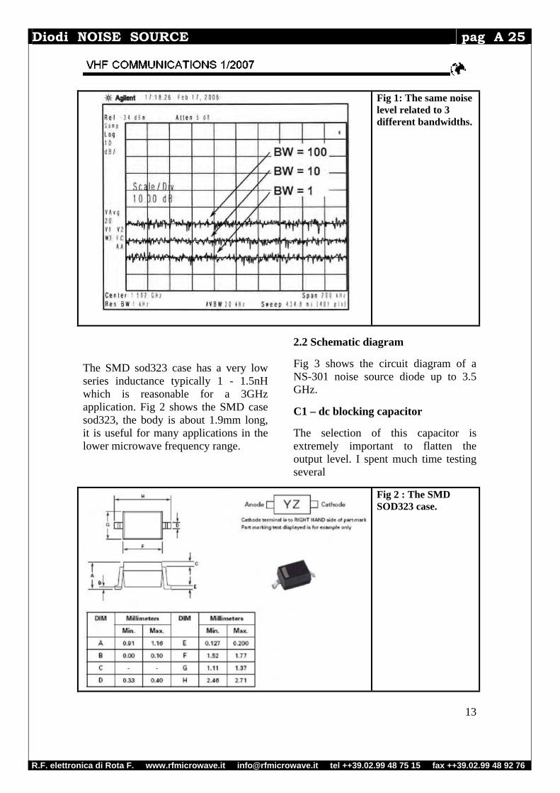
Fig 1: The same noise level related to 3 different bandwidths.
The SMD sod323 case has a very low series inductance typically 1 - 1.5nH which is reasonable for a 3GHz application. Fig 2 shows the SMD case sod323, the body is about 1.9mm long, it is useful for many applications in the lower microwave frequency range.
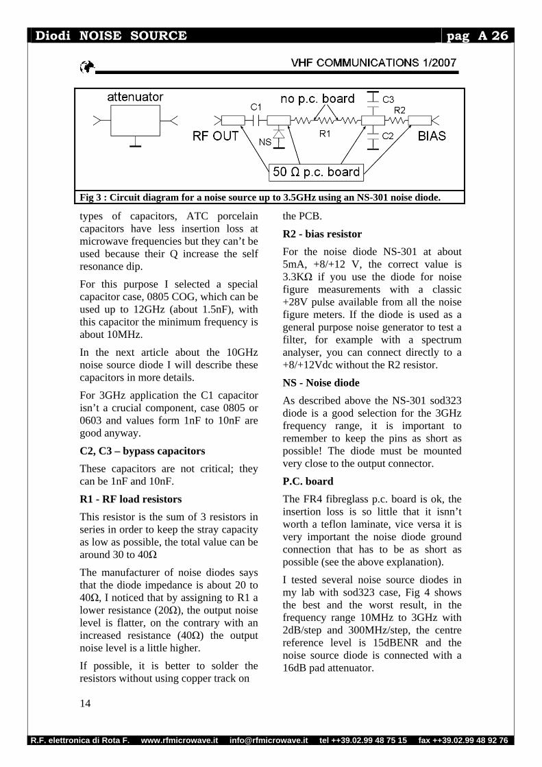
2.2 Schematic diagram Fig 3 shows the circuit diagram of a NS-301 noise source diode up to 3.5 GHz.
C1 – dc blocking capacitor The selection of this capacitor is extremely important to flatten the output level. I spent much time testing several
Fig 2 : The SMD SOD323 case.
13
R.F. elettronica di Rota F. www.rfmicrowave.it [email protected] tel ++39.02.99 48 75 15 fax ++39.02.99 48 92 76
Diodi NOISE SOURCE pag A 26
Fig 3 : Circuit diagram for a noise source up to 3.5GHz using an NS-301 noise diode.
types of capacitors, ATC porcelain capacitors have less insertion loss at microwave frequencies but they can’t be used because their Q increase the self resonance dip.
For this purpose I selected a special capacitor case, 0805 COG, which can be used up to 12GHz (about 1.5nF), with this capacitor the minimum frequency is about 10MHz.
In the next article about the 10GHz noise source diode I will describe these capacitors in more details.
For 3GHz application the C1 capacitor isn’t a crucial component, case 0805 or 0603 and values form 1nF to 10nF are good anyway.
C2, C3 – bypass capacitors
These capacitors are not critical; they can be 1nF and 10nF.
R1 - RF load resistors
This resistor is the sum of 3 resistors in series in order to keep the stray capacity as low as possible, the total value can be around 30 to 40Ω
The manufacturer of noise diodes says that the diode impedance is about 20 to 40Ω, I noticed that by assigning to R1 a lower resistance (20Ω), the output noise level is flatter, on the contrary with an increased resistance (40Ω) the output noise level is a little higher.
If possible, it is better to solder the resistors without using copper track on
the PCB.
R2 - bias resistor
For the noise diode NS-301 at about 5mA, +8/+12 V, the correct value is 3.3KΩ if you use the diode for noise figure measurements with a classic +28V pulse available from all the noise figure meters. If the diode is used as a general purpose noise generator to test a filter, for example with a spectrum analyser, you can connect directly to a +8/+12Vdc without the R2 resistor.
NS - Noise diode
As described above the NS-301 sod323 diode is a good selection for the 3GHz frequency range, it is important to remember to keep the pins as short as possible! The diode must be mounted very close to the output connector.
P.C. board
The FR4 fibreglass p.c. board is ok, the insertion loss is so little that it isnn’t worth a teflon laminate, vice versa it is very important the noise diode ground connection that has to be as short as possible (see the above explanation).
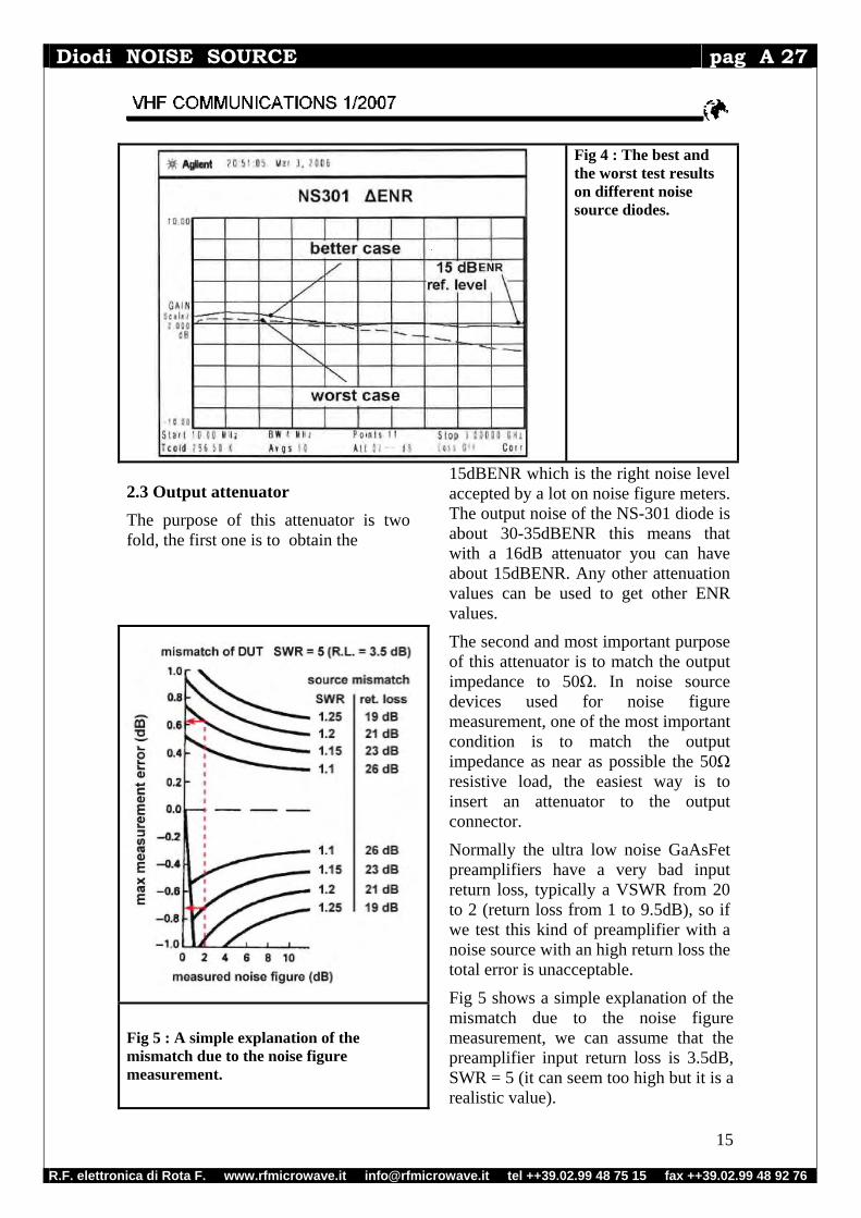
I tested several noise source diodes in my lab with sod323 case, Fig 4 shows the best and the worst result, in the frequency range 10MHz to 3GHz with 2dB/step and 300MHz/step, the centre reference level is 15dBENR and the noise source diode is connected with a 16dB pad attenuator.
14
R.F. elettronica di Rota F. www.rfmicrowave.it [email protected] tel ++39.02.99 48 75 15 fax ++39.02.99 48 92 76
Diodi NOISE SOURCE pag A 27
Fig 4 : The best and the worst test results on different noise source diodes.
2.3 Output attenuator
The purpose of this attenuator is two fold, the first one is to obtain the
Fig 5 : A simple explanation of the mismatch due to the noise figure measurement.
15dBENR which is the right noise level accepted by a lot on noise figure meters. The output noise of the NS-301 diode is about 30-35dBENR this means that with a 16dB attenuator you can have about 15dBENR. Any other attenuation values can be used to get other ENR values.
The second and most important purpose of this attenuator is to match the output impedance to 50Ω. In noise source devices used for noise figure measurement, one of the most important condition is to match the output impedance as near as possible the 50Ω resistive load, the easiest way is to insert an attenuator to the output connector.
Normally the ultra low noise GaAsFet preamplifiers have a very bad input return loss, typically a VSWR from 20 to 2 (return loss from 1 to 9.5dB), so if we test this kind of preamplifier with a noise source with an high return loss the total error is unacceptable.
Fig 5 shows a simple explanation of the mismatch due to the noise figure measurement, we can assume that the preamplifier input return loss is 3.5dB, SWR = 5 (it can seem too high but it is a realistic value).
15
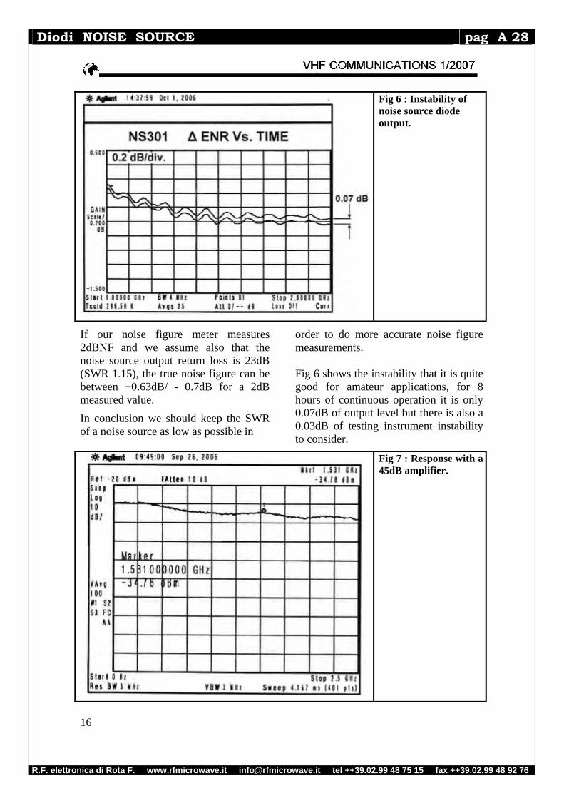
R.F. elettronica di Rota F. www.rfmicrowave.it [email protected] tel ++39.02.99 48 75 15 fax ++39.02.99 48 92 76
Diodi NOISE SOURCE pag A 28
Fig 6 : Instability of noise source diode output.
If our noise figure meter measures 2dBNF and we assume also that the noise source output return loss is 23dB (SWR 1.15), the true noise figure can be between +0.63dB/ - 0.7dB for a 2dB measured value.
In conclusion we should keep the SWR of a noise source as low as possible in
order to do more accurate noise figure measurements. Fig 6 shows the instability that it is quite good for amateur applications, for 8 hours of continuous operation it is only 0.07dB of output level but there is also a 0.03dB of testing instrument instability to consider.
Fig 7 : Response with a 45dB amplifier.
16
R.F. elettronica di Rota F. www.rfmicrowave.it [email protected] tel ++39.02.99 48 75 15 fax ++39.02.99 48 92 76
Diodi NOISE SOURCE pag A 29
Fig 8 : Picture of the broadband amplifier.
3.
General purpose noise generator
As shown in Table 1 a diode noise source can be used successfully in a broadband noise generator combined with a spectrum analyser like a “tracking generator”. This is not a true tracking generator because it works in a different way. As I said above the tracking generator is like a sweep generator so its frequency moves from start to end but it is not simultaneous in all the frequency range.
If we combine a broadband noise generator with a spectrum analyser we
can do a measurement of band pass filters, return loss etc. The signal coming from the noise generator diode is very low so we need at least 45dB of amplification, however 65dB is better. The real difficulty is to obtain a reasonable flat amplifier response. For this purpose I made an amplifier using INA03184 and INA10386 MMICs, the result is shown in Fig 7 and the total response is given by the noise source diode combined with the 45dB amplifier.
Figs 8 and 9 show the 45dB broadband amplifier from few MHz to 2.5GHz used as noise amplifier in order to test the 2GHz band pass filter. This circuit is not difficult to build and it can be used in any lab as general purpose broadband amplifier.
Fig 9 : Circuit diagram of the broadband amplifier.
17
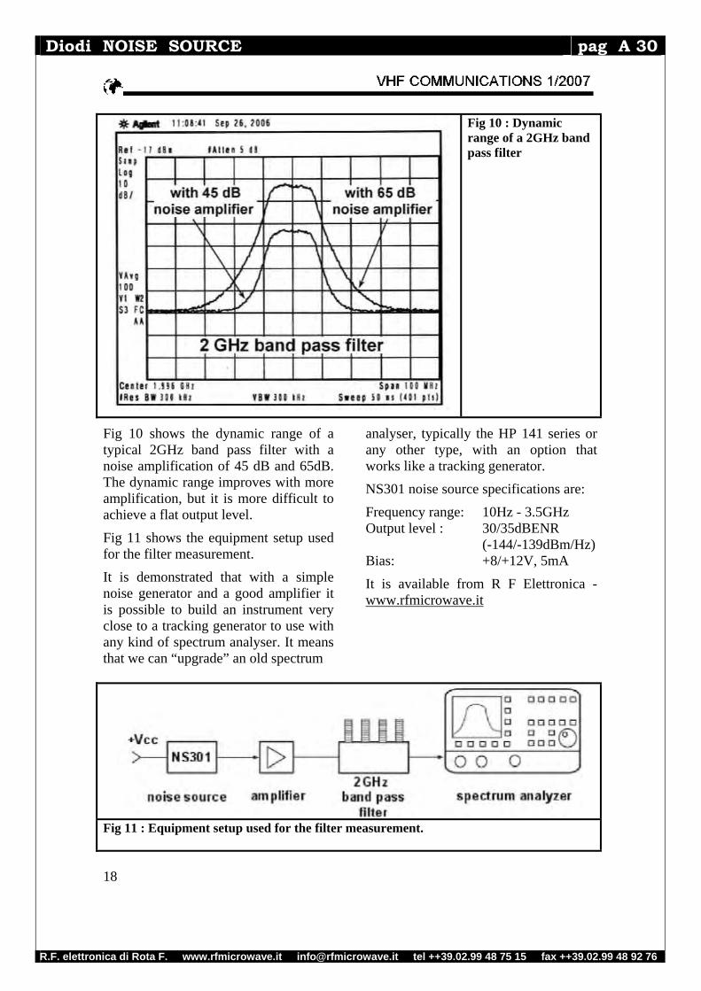
R.F. elettronica di Rota F. www.rfmicrowave.it [email protected] tel ++39.02.99 48 75 15 fax ++39.02.99 48 92 76
Diodi NOISE SOURCE pag A 30
Fig 10 : Dynamic range of a 2GHz band pass filter
Fig 10 shows the dynamic range of a typical 2GHz band pass filter with a noise amplification of 45 dB and 65dB. The dynamic range improves with more amplification, but it is more difficult to achieve a flat output level.
Fig 11 shows the equipment setup used for the filter measurement.
It is demonstrated that with a simple noise generator and a good amplifier it is possible to build an instrument very close to a tracking generator to use with any kind of spectrum analyser. It means that we can “upgrade” an old spectrum
analyser, typically the HP 141 series or any other type, with an option that works like a tracking generator.
NS301 noise source specifications are:
Frequency range: 10Hz - 3.5GHz Output level : 30/35dBENR (-144/-139dBm/Hz)Bias: +8/+12V, 5mA
It is available from R F Elettronica - www.rfmicrowave.it
Fig 11 : Equipment setup used for the filter measurement. 18
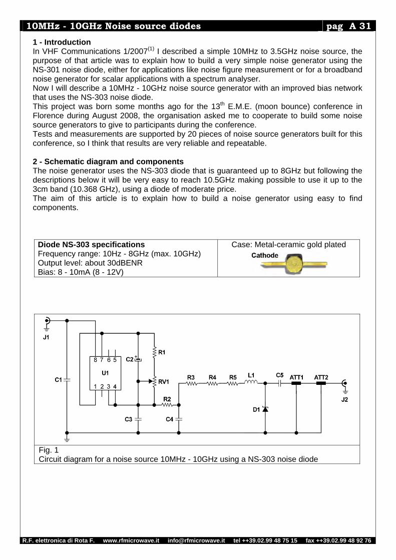
R.F. elettronica di Rota F. www.rfmicrowave.it [email protected] tel ++39.02.99 48 75 15 fax ++39.02.99 48 92 76
10MHz - 10GHz Noise source diodes pag A 31
1 - Introduction In VHF Communications 1/2007(1) I described a simple 10MHz to 3.5GHz noise source, the purpose of that article was to explain how to build a very simple noise generator using the NS-301 noise diode, either for applications like noise figure measurement or for a broadband noise generator for scalar applications with a spectrum analyser. Now I will describe a 10MHz - 10GHz noise source generator with an improved bias network that uses the NS-303 noise diode. This project was born some months ago for the 13th E.M.E. (moon bounce) conference in Florence during August 2008, the organisation asked me to cooperate to build some noise source generators to give to participants during the conference. Tests and measurements are supported by 20 pieces of noise source generators built for this conference, so I think that results are very reliable and repeatable. 2 - Schematic diagram and components The noise generator uses the NS-303 diode that is guaranteed up to 8GHz but following the descriptions below it will be very easy to reach 10.5GHz making possible to use it up to the 3cm band (10.368 GHz), using a diode of moderate price. The aim of this article is to explain how to build a noise generator using easy to find components.
Diode NS-303 specifications Frequency range: 10Hz - 8GHz (max. 10GHz) Output level: about 30dBENR Bias: 8 - 10mA (8 - 12V)
Case: Metal-ceramic gold plated
Fig. 1 Circuit diagram for a noise source 10MHz - 10GHz using a NS-303 noise diode
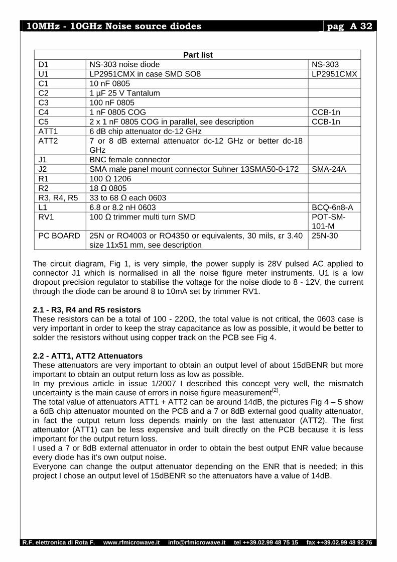
R.F. elettronica di Rota F. www.rfmicrowave.it [email protected] tel ++39.02.99 48 75 15 fax ++39.02.99 48 92 76
10MHz - 10GHz Noise source diodes pag A 32
Part list D1 NS-303 noise diode NS-303 U1 LP2951CMX in case SMD SO8 LP2951CMXC1 10 nF 0805 C2 1 µF 25 V Tantalum C3 100 nF 0805 C4 1 nF 0805 COG CCB-1n C5 2 x 1 nF 0805 COG in parallel, see description CCB-1n ATT1 6 dB chip attenuator dc-12 GHz ATT2 7 or 8 dB external attenuator dc-12 GHz or better dc-18
GHz
J1 BNC female connector J2 SMA male panel mount connector Suhner 13SMA50-0-172 SMA-24A R1 100 Ω 1206 R2 18 Ω 0805 R3, R4, R5 33 to 68 Ω each 0603 L1 6.8 or 8.2 nH 0603 BCQ-6n8-A RV1 100 Ω trimmer multi turn SMD POT-SM-
101-M PC BOARD 25N or RO4003 or RO4350 or equivalents, 30 mils, εr 3.40
size 11x51 mm, see description 25N-30
The circuit diagram, Fig 1, is very simple, the power supply is 28V pulsed AC applied to connector J1 which is normalised in all the noise figure meter instruments. U1 is a low dropout precision regulator to stabilise the voltage for the noise diode to 8 - 12V, the current through the diode can be around 8 to 10mA set by trimmer RV1. 2.1 - R3, R4 and R5 resistors These resistors can be a total of 100 - 220Ω, the total value is not critical, the 0603 case is very important in order to keep the stray capacitance as low as possible, it would be better to solder the resistors without using copper track on the PCB see Fig 4. 2.2 - ATT1, ATT2 Attenuators These attenuators are very important to obtain an output level of about 15dBENR but more important to obtain an output return loss as low as possible. In my previous article in issue 1/2007 I described this concept very well, the mismatch uncertainty is the main cause of errors in noise figure measurement(2). The total value of attenuators ATT1 + ATT2 can be around 14dB, the pictures Fig 4 – 5 show a 6dB chip attenuator mounted on the PCB and a 7 or 8dB external good quality attenuator, in fact the output return loss depends mainly on the last attenuator (ATT2). The first attenuator (ATT1) can be less expensive and built directly on the PCB because it is less important for the output return loss. I used a 7 or 8dB external attenuator in order to obtain the best output ENR value because every diode has it’s own output noise. Everyone can change the output attenuator depending on the ENR that is needed; in this project I chose an output level of 15dBENR so the attenuators have a value of 14dB.
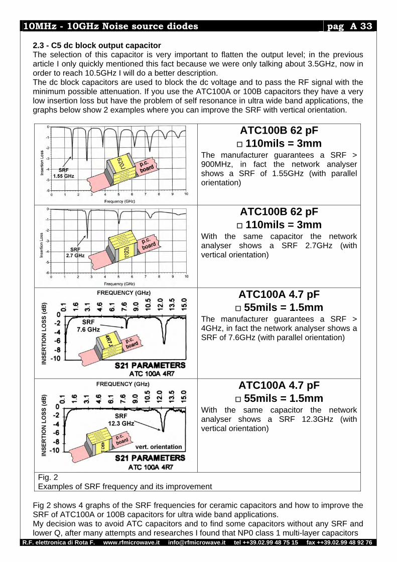
R.F. elettronica di Rota F. www.rfmicrowave.it [email protected] tel ++39.02.99 48 75 15 fax ++39.02.99 48 92 76
10MHz - 10GHz Noise source diodes pag A 33
2.3 - C5 dc block output capacitor The selection of this capacitor is very important to flatten the output level; in the previous article I only quickly mentioned this fact because we were only talking about 3.5GHz, now in order to reach 10.5GHz I will do a better description. The dc block capacitors are used to block the dc voltage and to pass the RF signal with the minimum possible attenuation. If you use the ATC100A or 100B capacitors they have a very low insertion loss but have the problem of self resonance in ultra wide band applications, the graphs below show 2 examples where you can improve the SRF with vertical orientation.
ATC100B 62 pF 110mils = 3mm
The manufacturer guarantees a SRF > 900MHz, in fact the network analyser shows a SRF of 1.55GHz (with parallel orientation)
ATC100B 62 pF 110mils = 3mm
With the same capacitor the network analyser shows a SRF 2.7GHz (with vertical orientation)
ATC100A 4.7 pF 55mils = 1.5mm
The manufacturer guarantees a SRF > 4GHz, in fact the network analyser shows a SRF of 7.6GHz (with parallel orientation)
ATC100A 4.7 pF 55mils = 1.5mm
With the same capacitor the network analyser shows a SRF 12.3GHz (with vertical orientation)
Fig. 2 Examples of SRF frequency and its improvement
Fig 2 shows 4 graphs of the SRF frequencies for ceramic capacitors and how to improve the SRF of ATC100A or 100B capacitors for ultra wide band applications. My decision was to avoid ATC capacitors and to find some capacitors without any SRF and lower Q, after many attempts and researches I found that NP0 class 1 multi-layer capacitors
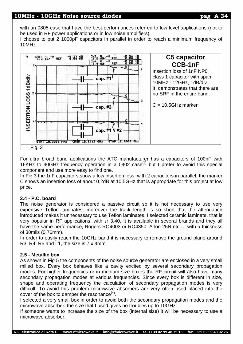
R.F. elettronica di Rota F. www.rfmicrowave.it [email protected] tel ++39.02.99 48 75 15 fax ++39.02.99 48 92 76
10MHz - 10GHz Noise source diodes pag A 34
with an 0805 case that have the best performances referred to low level applications (not to be used in RF power applications or in low noise amplifiers). I choose to put 2 1000pF capacitors in parallel in order to reach a minimum frequency of 10MHz.
C5 capacitor CCB-1nF
Insertion loss of 1nF NP0 class 1 capacitor with span 10MHz - 12GHz, 1dB/div. It demonstrates that there are no SRF in the entire band. C = 10.5GHz marker
Fig. 3 For ultra broad band applications the ATC manufacturer has a capacitors of 100nF with 16KHz to 40GHz frequency operation in a 0402 case(3) but I prefer to avoid this special component and use more easy to find one. In Fig 3 the 1nF capacitors show a low insertion loss, with 2 capacitors in parallel, the marker C shows an insertion loss of about 0.2dB at 10.5GHz that is appropriate for this project at low price. 2.4 - P.C. board The noise generator is considered a passive circuit so it is not necessary to use very expensive Teflon laminates, moreover the track length is so short that the attenuation introduced makes it unnecessary to use Teflon laminates. I selected ceramic laminate, that is very popular in RF applications, with εr 3.40. It is available in several brands and they all have the same performance, Rogers RO4003 or RO4350, Arlon 25N etc…, with a thickness of 30mils (0.76mm). In order to easily reach the 10GHz band it is necessary to remove the ground plane around R3, R4, R5 and L1, the size is 7 x 4mm 2.5 - Metallic box As shown in Fig 5 the components of the noise source generator are enclosed in a very small milled box. Every box behaves like a cavity excited by several secondary propagation modes. For higher frequencies or in medium size boxes the RF circuit will also have many secondary propagation modes at various frequencies. Since every box is different in size, shape and operating frequency the calculation of secondary propagation modes is very difficult. To avoid this problem microwave absorbers are very often used placed into the cover of the box to damper the resonance(4). I selected a very small box in order to avoid both the secondary propagation modes and the microwave absorber; the size that I used gives no troubles up to 10GHz. If someone wants to increase the size of the box (internal size) it will be necessary to use a microwave absorber.
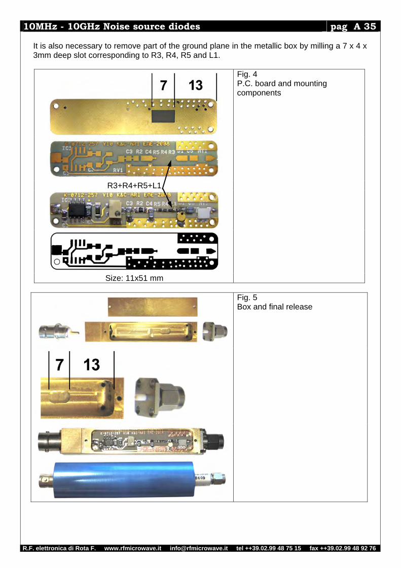
R.F. elettronica di Rota F. www.rfmicrowave.it [email protected] tel ++39.02.99 48 75 15 fax ++39.02.99 48 92 76
10MHz - 10GHz Noise source diodes pag A 35
It is also necessary to remove part of the ground plane in the metallic box by milling a 7 x 4 x 3mm deep slot corresponding to R3, R4, R5 and L1.
R3+R4+R5+L1
Size: 11x51 mm
Fig. 4 P.C. board and mounting components
Fig. 5 Box and final release
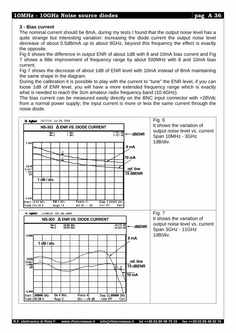
R.F. elettronica di Rota F. www.rfmicrowave.it [email protected] tel ++39.02.99 48 75 15 fax ++39.02.99 48 92 76
10MHz - 10GHz Noise source diodes pag A 36
3 - Bias current The nominal current should be 8mA, during my tests I found that the output noise level has a quite strange but interesting variation: increasing the diode current the output noise level decrease of about 0.5dB/mA up to about 9GHz, beyond this frequency the effect is exactly the opposite. Fig 6 shows the difference in output ENR of about 1dB with 8 and 10mA bias current and Fig 7 shows a little improvement of frequency range by about 500MHz with 8 and 10mA bias current. Fig 7 shows the decrease of about 1dB of ENR level with 10mA instead of 8mA maintaining the same shape in the diagram. During the calibration it is possible to play with the current to “tune” the ENR level, if you can loose 1dB of ENR level, you will have a more extended frequency range which is exactly what is needed to reach the 3cm amateur radio frequency band (10.4GHz). The bias current can be measured easily directly on the BNC input connector with +28Vdc from a normal power supply; the input current is more or less the same current through the noise diode.
Fig. 6 It shows the variation of output noise level vs. currentSpan 10MHz - 3GHz 1dB/div.
Fig. 7 It shows the variation of output noise level vs. currentSpan 3GHz - 11GHz 1dB/div.
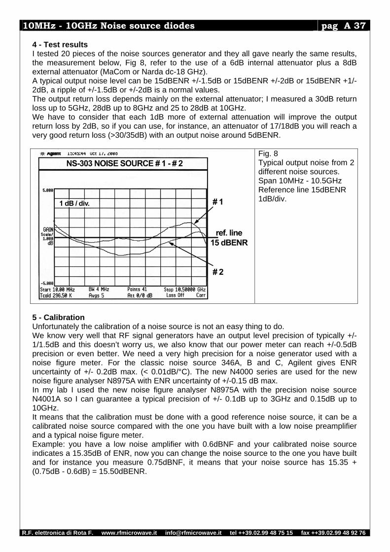
R.F. elettronica di Rota F. www.rfmicrowave.it [email protected] tel ++39.02.99 48 75 15 fax ++39.02.99 48 92 76
10MHz - 10GHz Noise source diodes pag A 37 4 - Test results I tested 20 pieces of the noise sources generator and they all gave nearly the same results, the measurement below, Fig 8, refer to the use of a 6dB internal attenuator plus a 8dB external attenuator (MaCom or Narda dc-18 GHz). A typical output noise level can be 15dBENR +/-1.5dB or 15dBENR +/-2dB or 15dBENR +1/-2dB, a ripple of +/-1.5dB or +/-2dB is a normal values. The output return loss depends mainly on the external attenuator; I measured a 30dB return loss up to 5GHz, 28dB up to 8GHz and 25 to 28dB at 10GHz. We have to consider that each 1dB more of external attenuation will improve the output return loss by 2dB, so if you can use, for instance, an attenuator of 17/18dB you will reach a very good return loss (>30/35dB) with an output noise around 5dBENR.
Fig. 8 Typical output noise from 2 different noise sources. Span 10MHz - 10.5GHz Reference line 15dBENR 1dB/div.
5 - Calibration Unfortunately the calibration of a noise source is not an easy thing to do. We know very well that RF signal generators have an output level precision of typically +/- 1/1.5dB and this doesn’t worry us, we also know that our power meter can reach +/-0.5dB precision or even better. We need a very high precision for a noise generator used with a noise figure meter. For the classic noise source 346A, B and C, Agilent gives ENR uncertainty of +/- 0.2dB max. (< 0.01dB/°C). The new N4000 series are used for the new noise figure analyser N8975A with ENR uncertainty of +/-0.15 dB max. In my lab I used the new noise figure analyser N8975A with the precision noise source N4001A so I can guarantee a typical precision of +/- 0.1dB up to 3GHz and 0.15dB up to 10GHz. It means that the calibration must be done with a good reference noise source, it can be a calibrated noise source compared with the one you have built with a low noise preamplifier and a typical noise figure meter. Example: you have a low noise amplifier with 0.6dBNF and your calibrated noise source indicates a 15.35dB of ENR, now you can change the noise source to the one you have built and for instance you measure 0.75dBNF, it means that your noise source has 15.35 + (0.75dB - 0.6dB) = 15.50dBENR.
R.F. elettronica di Rota F. www.rfmicrowave.it [email protected] tel ++39.02.99 48 75 15 fax ++39.02.99 48 92 76
10MHz - 10GHz Noise source diodes pag A 38
6 - Other application As I described in the previous article(1) that the noise source can be used as a broadband noise generator combined with a spectrum analyser like a “tracking generator” for scalar applications. This is not a true tracking generator because it works in a different way (read my previous article(1)). The problem here is to reach 3 decades of frequency range, 10MHz to 10GHz, with a flat amplifier of at least 50dB. Today some MMICs are available that can do this work like ERA1, ERA2, MGA86576 etc…, the problems can be to reach a flat amplification and to avoid self oscillations with such high amplification. This device can be very interesting because it can be a useful tool to use with any kind of obsolete spectrum analyser to tune filters, to measure the return loss etc… up to 10GHz. For anymore informations regarding noise source diodes see www.rfmicrowave.it/pdf/diodi.pdf (from page A 14) Notes: (1) VHF Communications 1/2007 “Noise source diodes” (2) For those who need more information about the mismatch uncertainty in noise figure
measurement I suggest 3 application notes: - Ham Radio, August 1978 - Noise figure measurement accuracy AN57-2 Agilent - Calculating mismatch uncertainty, Microwave Journal May 2008
(3) R.F. Elettronica web site catalogue www.rfmicrowave.it (capacitors section) (4) VHF Communications 4/2004 “Franco’s finest microwave absorber”
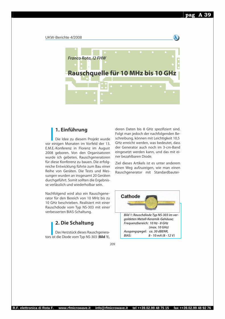
R.F. elettronica di Rota F. www.rfmicrowave.it [email protected] tel ++39.02.99 48 75 15 fax ++39.02.99 48 92 76
pag A 39
I
I
UKW-Berichte 4/2008
Franco Rota, I2 FHW
Rauschquelle für 10 MHz bis 10 GHz
1. Einführung
Die Idee zu diesem Projekt wurde vor einigen Monaten im Vorfeld der 13. E.M.E.-Konferenz in Florenz im August 2008 geboren. Von den Organisatoren wurde ich gebeten, Rauschgeneratoren für diese Konferenz zu bauen. Die erfolg- reiche Entwicklung führte zum Bau einer Reihe von Geräten. Die Tests und Mes- sungen wurden an insgesamt 20 Geräten durchgeführt. Somit sollten die Ergebnis- se verlässlich und wiederholbar sein.
deren Daten bis 8 GHz spezifiziert sind. Folgt man jedoch der nachfolgenden Be- schreibung, können mit Leichtigkeit 10,5 GHz erreicht werden, was bedeutet, dass der Generator auch noch im 3-cm-Band eingesetzt werden kann, und das mit ei- ner bezahlbaren Diode.
Ziel dieses Artikels ist es unter anderem einen Weg aufzuzeigen, wie man einen Rauschgenerator mit Standardbautei-
Nachfolgend wird also ein Rauschgene- rator für den Bereich von 10 MHz bis zu 10 GHz beschrieben. Realisiert mit einer Rauschdiode vom Typ NS-303 mit einer verbesserten BIAS-Schaltung.
2. Die Schaltung
Das Herzstück dieses Rauschgenera-
tors ist die Diode vom Typ NS-303 (Bild 1),
209
Bild 1: Rauschdiode Typ NS-303 im ver- goldeten Metall-Keramik-Gehäuse; Frequenzbereich: 10 Hz - 8 GHz
(max. 10 GHz) Ausgangspegel: ca. 30 dBENR, BIAS: 8 - 10 mA (8 - 12 V)
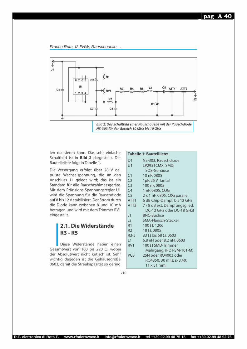
R.F. elettronica di Rota F. www.rfmicrowave.it [email protected] tel ++39.02.99 48 75 15 fax ++39.02.99 48 92 76
pag A 40
I
Franco Rota, I2 FHW, Rauschquelle ...
Bild 2: Das Schaltbild einer Rauschquelle mit der Rauschdiode NS-303 für den Bereich 10 MHz bis 10 GHz
len realisieren kann. Das sehr einfache Schaltbild ist in Bild 2 dargestellt. Die Bauteileliste folgt in Tabelle 1.
Die Versorgung erfolgt über 28 V ge- pulste Wechselspannung, die an den Anschluss J1 gelegt wird; das ist ein Standard für alle Rauschzahlmessgeräte. Mit dem Präzisions-Spannungsregler U1 wird die Spannung für die Rauschdiode auf 8 bis 12 V stabilisiert. Der Strom durch die Diode kann zwischen 8 und 10 mA betragen und wird mit dem Trimmer RV1 eingestellt.
2.1. Die Widerstände R3 - R5
Diese Widerstände haben einen
Gesamtwert von 100 bis 220 Ω, wobei der Absolutwert nicht kritisch ist. Sehr wichtig dagegen ist die Gehäusegröße 0603, damit die Streukapazität so gering
210
Tabelle 1: Bauteilliste:
D1 NS-303, Rauschdiode U1 LP2951CMX, SMD,
SO8-Gehäuse C1 10 nF, 0805 C2 1μF, 25 V, Tantal C3 100 nF, 0805 C4 1 nF, 0805, COG C5 2 x 1 nF, 0805, C0G parallel ATT1 6 dB Chip-Dämpf. bis 12 GHz ATT2 7 / 8 dB ext. Dämpfungsglied,
DC-12 GHz oder DC-18 GHz! J1 BNC-Buchse J2 SMA-Flansch-Stecker R1 100 Ω, 1206 R2 18 Ω, 0805 R3-5 33 Ω bis 68 Ω, 0603 L1 6,8 nH oder 8,2 nH, 0603 RV1 100 Ω SMD-Trimmer,
Mehrgang, (POT-SM-101-M) PCB 25N oder RO4003 oder
RO4350; 30 mils; εr 3,40; 11 x 51 mm
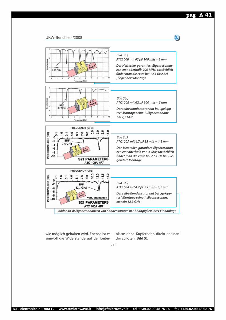
R.F. elettronica di Rota F. www.rfmicrowave.it [email protected] tel ++39.02.99 48 75 15 fax ++39.02.99 48 92 76
pag A 41
UKW-Berichte 4/2008
Bild 3a.) ATC100B mit 62 pF 100 mils = 3 mm
Der Hersteller garantiert Eigenresonan- zen erst oberhalb 900 MHz; tatsächlich findet man die erste bei 1,55 GHz bei „liegender“ Montage
Bild 3b.) ATC100B mit 62 pF 100 mils = 3 mm
Der selbe Kondensator hat bei „gekipp- ter“ Montage seine 1. Eigenresonanz bei 2,7 GHz
Bild 3c.) ATC100A mit 4,7 pF 55 mils = 1,5 mm
Der Hersteller garaniert Eigenresonan- zen erst oberhalb von 4 GHz; tatsächlich findet man die erste bei 7,6 GHz bei „lie- gender“ Montage
Bild 3d.) ATC100A mit 4,7 pF 55 mils = 1,5 mm
Der selbe Kondensator hat bei „gekipp- ter“ Montage seine 1. Eigenresonanz erst ein 12,3 GHz
Bilder 3a-d: Eigenresonanzen von Kondensatoren in Abhängigkeit ihrer Einbaulage
wie möglich gehalten wird. Ebenso ist es sinnvoll die Widerstände auf der Leiter-
platte ohne Kupferbahn direkt aneinan- der zu löten (Bild 5).
211
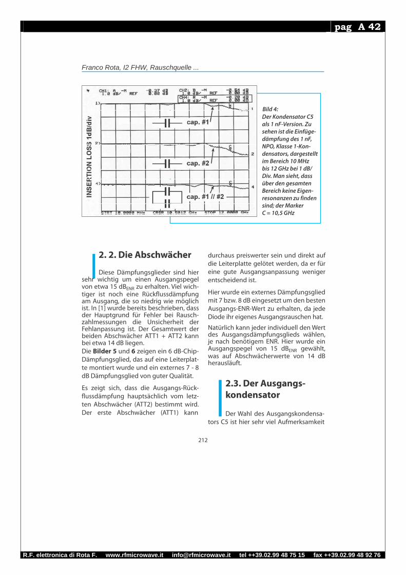
R.F. elettronica di Rota F. www.rfmicrowave.it [email protected] tel ++39.02.99 48 75 15 fax ++39.02.99 48 92 76
pag A 42
I
I
Franco Rota, I2 FHW, Rauschquelle ...
2. 2. Die Abschwächer
Diese Dämpfungsglieder sind hier sehr wichtig um einen Ausgangspegel von etwa 15 dBENR zu erhalten. Viel wich- tiger ist noch eine Rückflussdämpfung am Ausgang, die so niedrig wie möglich ist. In [1] wurde bereits beschrieben, dass der Hauptgrund für Fehler bei Rausch- zahlmessungen die Unsicherheit der Fehlanpassung ist. Der Gesamtwert der beiden Abschwächer ATT1 + ATT2 kann bei etwa 14 dB liegen. Die Bilder 5 und 6 zeigen ein 6 dB-Chip- Dämpfungsglied, das auf eine Leiterplat- te montiert wurde und ein externes 7 - 8 dB Dämpfungsglied von guter Qualität.
Es zeigt sich, dass die Ausgangs-Rück- flussdämpfung hauptsächlich vom letz- ten Abschwächer (ATT2) bestimmt wird. Der erste Abschwächer (ATT1) kann
212
Bild 4: Der Kondensator C5 als 1 nF-Version. Zu sehen ist die Einfüge- dämpfung des 1 nF, NPO, Klasse 1-Kon- densators, dargestellt im Bereich 10 MHz bis 12 GHz bei 1 dB/ Div. Man sieht, dass über den gesamten Bereich keine Eigen- resonanzen zu finden sind; der Marker C = 10,5 GHz
durchaus preiswerter sein und direkt auf die Leiterplatte gelötet werden, da er für eine gute Ausgangsanpassung weniger entscheidend ist.
Hier wurde ein externes Dämpfungsglied mit 7 bzw. 8 dB eingesetzt um den besten Ausgangs-ENR-Wert zu erhalten, da jede Diode ihr eigenes Ausgangsrauschen hat.
Natürlich kann jeder individuell den Wert des Ausgangsdämpfungsglieds wählen, je nach benötigem ENR. Hier wurde ein Ausgangspegel von 15 dBENR gewählt, was auf Abschwächerwerte von 14 dB herausläuft.
2.3. Der Ausgangs- kondensator
Der Wahl des Ausgangskondensa-
tors C5 ist hier sehr viel Aufmerksamkeit
R.F. elettronica di Rota F. www.rfmicrowave.it [email protected] tel ++39.02.99 48 75 15 fax ++39.02.99 48 92 76
pag A 43
UKW-Berichte 4/2008
Bilder 5: Massefläche mit Aussparung; Layout der SMD- Bestückungsseite; bestückte Leiterplatte und Layout der kleinen Leiterplatte für die Rauschquelle
zu schenken! Hat er doch gewaltigen Ein- fluss auf die Ebenheit des Ausgangspe- gels, zumal das Ausgangssignal ja hinauf bis 10,5 GHz reichen soll.
Der Ausgangskondensator soll die Gleichspannung auf dem Ausgangssi- gnal abblocken und lediglich das HF- Signal mit geringstmöglichen Verlusten durchlassen.
Verwendet man beispielsweise SMD- Kondensatoren vom Typ ATC100A oder 100B, so haben diese eine sehr geringe Einfügedämpfung. Jedoch haben diese
in Breitbandanwendungen das Problem von Eigenresonanzen. Dies kann man etwas verbessern, indem man die Chip- Kondensatoren nicht liegend, sondern seitlich gekippt einbaut (Bild 3).
In den einzelnen Teilbildern von Bild 3 sind jeweils die Orientierung (Monta- gerichtung) der ATC-Kondensatoren ATC100B und darunter ATC100A gezeigt. Jeweils im Hintergrund sind die Eigenre- sonanzkurven über der Frequenzachse dargestellt.
Um die Eigenresonanzen der ATC-Kon-
213
R.F. elettronica di Rota F. www.rfmicrowave.it [email protected] tel ++39.02.99 48 75 15 fax ++39.02.99 48 92 76
pag A 44
I
Franco Rota, I2 FHW, Rauschquelle ...
Bild6: Das schmale Alu-Fräsgehäu- se mit BNC- und SMA-Anschlüs- sen; darunter im Detail die Bemaßung der Vertiefung im Gehäuse (siehe Text)
densatoren zu vermeiden, wurde nach Alternativen Ausschau gehalten, die möglichst keine Resonanzstellen und ein niedrigeres Q haben. Viele Bauteile wur- den überprüft und gemessen, bis sich folgendes Ergebnis zeigte: Multilayer- Kondensatoren (Klasse 1) in der Größe 0805 mit Material NPO zeigen hier, also für Kleinleistungsanwendung, das beste Verhalten, (sie sind jedoch für HF-Leis- tungsanwendungen oder für rauscharme Verstärker ungeeignet!).
Gewählt wurde hier die Parallelschaltung von zwei 1000 pF-Kondensatoren um auch nach unten minimal bis 10 MHz zu kommen.
Speziell für Breitband-Anwendungen wird von ATC ein 100 nF-Kondensator in der Bauform 0402 [3] angeboten; nach- dem dies jedoch ein Spezialbauteil ist, wurden die oben beschriebenen leichter verfügbaren Bauteile bevorzugt.
Die geringe Einfügedämpfung der 1 nF- Kondensatoren ist in Bild 4 dargestellt. Die Parallelschaltung der beiden Konden- satoren bringt auf 10,5 GHz (Marker C) eine Einfügedämpfung von lediglich 0,2 dB; das ist für dieses Projekt in Ordnung - und das zu einem günstigen Preis.
2.4. Die Leiterplatte
Der Rauschgenerator sollte eigent- lich eine passive Schaltung sein, weshalb keine teure Teflon-Leiterplatte erforder- lich ist. Außerdem sind die Leitungslän- gen sehr kurz und die verursachten Ver- luste noch akzeptabel - also kein Teflon.
Gewählt wurde hier ein Keramik-Lami- nat, was für HF-Anwendungen durchaus üblich ist, mit einem εr von 3,40. Dieses gibt es von verschiedenen Herstellern mit vergleichbaren Eigenschaften: RO- GERS RO4003 oder RO4350, Arlon 25N
214
R.F. elettronica di Rota F. www.rfmicrowave.it [email protected] tel ++39.02.99 48 75 15 fax ++39.02.99 48 92 76
pag A 45
I
UKW-Berichte 4/2008
Bild 6b: Die bestückte Leiterplatte fertig eingebaut in das Fräsgehäuse; darunter das „Endprodukt“ mit externem Dämpfungslied (rechts)
u.s.w. jeweils mit einer Stärke von 30 mils (0,75 mm).
Um auch wirklich noch das 10 GHz-Band abdecken zu können, ist es erforderlich die Massefläche um R3, R4, R5 und L1 zu entfernen; die Maße sind 7 mm x 4 mm (Bild 5).
2.5. Das Metallgehäuse
Die Bauteile des Rauschgenerators
werden in ein sehr kleines gefrästes Alu- gehäuse eingebaut. Leider verhält sich jedes Gehäuse wie ein Hohlleiter mit et- lichen Ausbreitungsmoden. Für höhere Frequenzen oder für mittelgroße Gehäu- se wird die HF-Schaltung ebenfalls etli- che sekundäre Ausbreitungsmodus auf verschiedensten Frequenzen haben.
Da jedes Gehäuse eine unterschiedliche Größe und Form hat und die Arbeitsfre-
215
quenzen der eingebauten Schaltungen unterschiedlich sind, ist die Berechnung der sekundären Ausbreitungsmodi sehr schwierig.
Um dieses Problem zu umgehen, werden häufig Mikrowellenabsorbermaterialien (z.B. leitfähiger Schaumstoff ) eingesetzt, die z.B. in den Gehäusedeckel geklebt werden. Damit versucht man mögliche Resonanzen zu bedämpfen oder zu ver- hindern.
Der Versuch, all diesen Problemen aus dem Weg zu gehen, führte zu einem sehr kleinen Gehäuse, das problemlos bis 10 GHz einsetzbar ist. Möchte jemand die Innenmaße größer gestalten, wird wie- der Absorbermaterial notwendig wer- den. Weiterhin ist es notwendig, einen 3 mm tiefen Spalt (7 mm x 4 mm) unter den Widerständen R3, R4, R5 und L1 aus dem Gehäuseboden zu fräsen, damit der Ab- stand zur Massefläche größer wird.
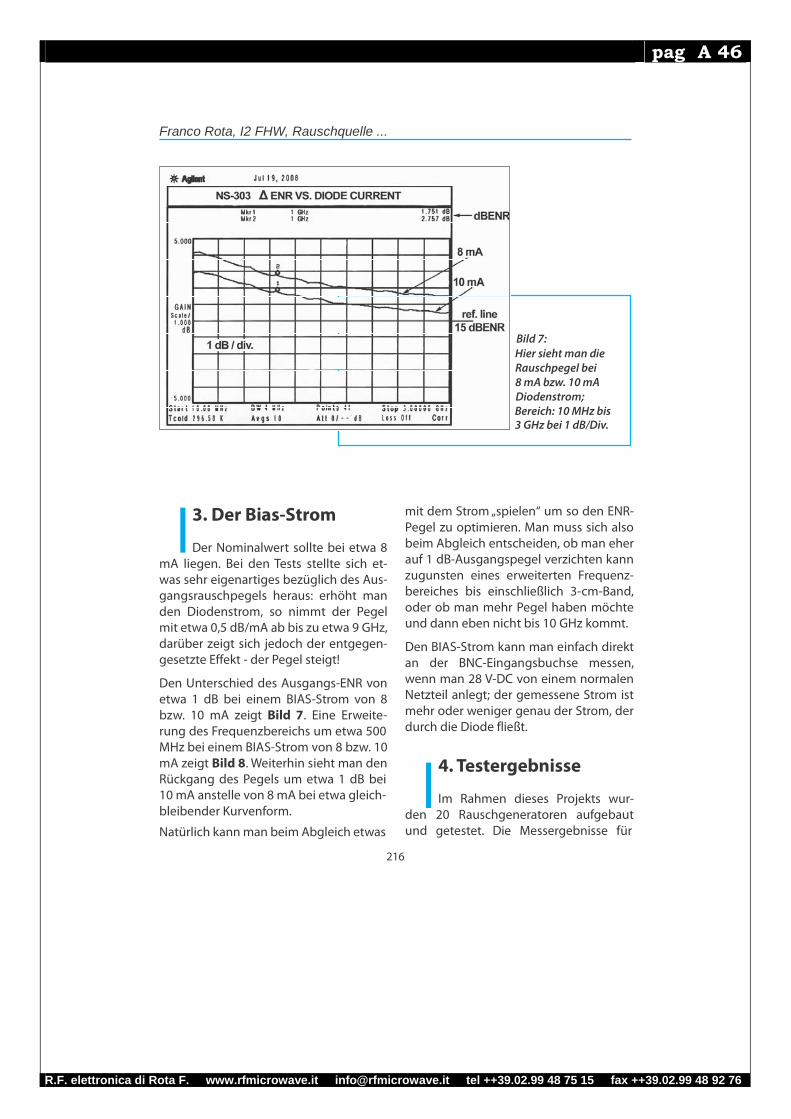
R.F. elettronica di Rota F. www.rfmicrowave.it [email protected] tel ++39.02.99 48 75 15 fax ++39.02.99 48 92 76
pag A 46
I
I
Franco Rota, I2 FHW, Rauschquelle ...
Bild 7: Hier sieht man die Rauschpegel bei 8 mA bzw. 10 mA Diodenstrom; Bereich: 10 MHz bis 3 GHz bei 1 dB/Div.
3. Der Bias-Strom
Der Nominalwert sollte bei etwa 8 mA liegen. Bei den Tests stellte sich et- was sehr eigenartiges bezüglich des Aus- gangsrauschpegels heraus: erhöht man den Diodenstrom, so nimmt der Pegel mit etwa 0,5 dB/mA ab bis zu etwa 9 GHz, darüber zeigt sich jedoch der entgegen- gesetzte Effekt - der Pegel steigt!
Den Unterschied des Ausgangs-ENR von etwa 1 dB bei einem BIAS-Strom von 8 bzw. 10 mA zeigt Bild 7. Eine Erweite- rung des Frequenzbereichs um etwa 500 MHz bei einem BIAS-Strom von 8 bzw. 10 mA zeigt Bild 8. Weiterhin sieht man den Rückgang des Pegels um etwa 1 dB bei 10 mA anstelle von 8 mA bei etwa gleich- bleibender Kurvenform.
Natürlich kann man beim Abgleich etwas
216
mit dem Strom „spielen“ um so den ENR- Pegel zu optimieren. Man muss sich also beim Abgleich entscheiden, ob man eher auf 1 dB-Ausgangspegel verzichten kann zugunsten eines erweiterten Frequenz- bereiches bis einschließlich 3-cm-Band, oder ob man mehr Pegel haben möchte und dann eben nicht bis 10 GHz kommt.
Den BIAS-Strom kann man einfach direkt an der BNC-Eingangsbuchse messen, wenn man 28 V-DC von einem normalen Netzteil anlegt; der gemessene Strom ist mehr oder weniger genau der Strom, der durch die Diode fließt.
4. Testergebnisse
Im Rahmen dieses Projekts wur- den 20 Rauschgeneratoren aufgebaut und getestet. Die Messergebnisse für
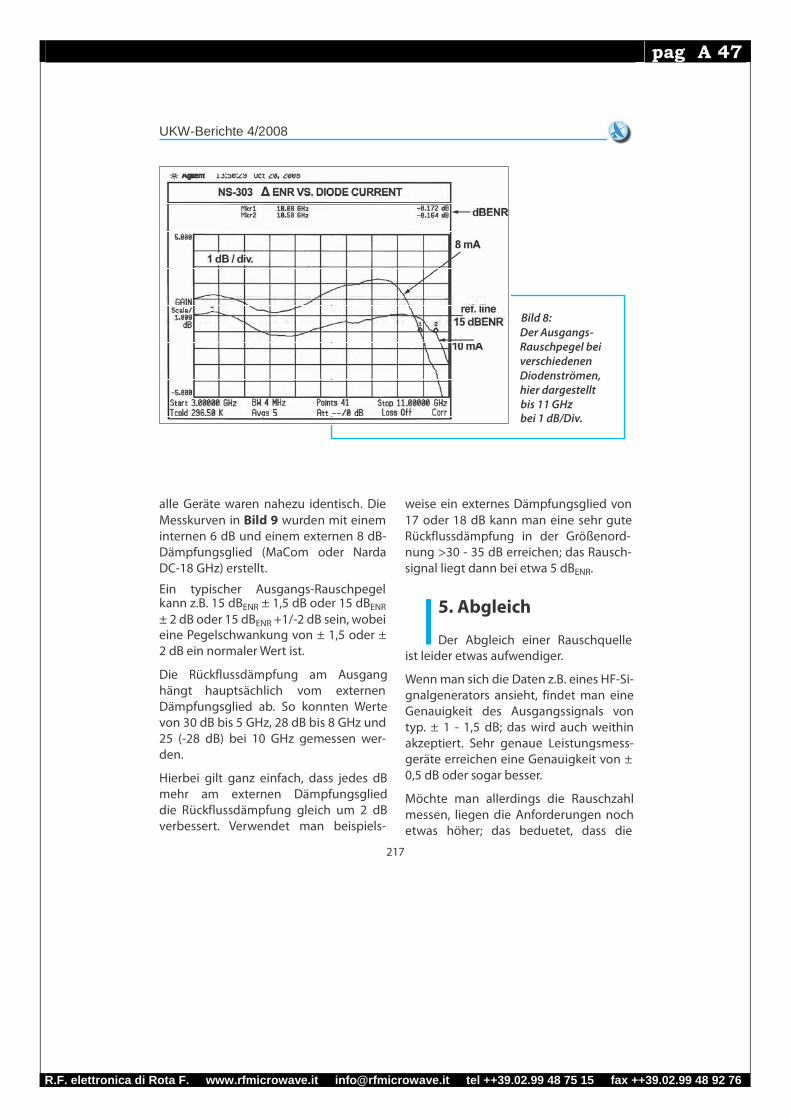
R.F. elettronica di Rota F. www.rfmicrowave.it [email protected] tel ++39.02.99 48 75 15 fax ++39.02.99 48 92 76
pag A 47
I
UKW-Berichte 4/2008
Bild 8: Der Ausgangs- Rauschpegel bei verschiedenen Diodenströmen, hier dargestellt bis 11 GHz bei 1 dB/Div.
alle Geräte waren nahezu identisch. Die Messkurven in Bild 9 wurden mit einem internen 6 dB und einem externen 8 dB- Dämpfungsglied (MaCom oder Narda DC-18 GHz) erstellt.
Ein typischer Ausgangs-Rauschpegel kann z.B. 15 dBENR ± 1,5 dB oder 15 dBENR
± 2 dB oder 15 dBENR +1/-2 dB sein, wobei eine Pegelschwankung von ± 1,5 oder ±
weise ein externes Dämpfungsglied von 17 oder 18 dB kann man eine sehr gute Rückflussdämpfung in der Größenord- nung >30 - 35 dB erreichen; das Rausch- signal liegt dann bei etwa 5 dBENR.
5. Abgleich
Der Abgleich einer Rauschquelle 2 dB ein normaler Wert ist.
Die Rückflussdämpfung am Ausgang hängt hauptsächlich vom externen Dämpfungsglied ab. So konnten Werte von 30 dB bis 5 GHz, 28 dB bis 8 GHz und 25 (-28 dB) bei 10 GHz gemessen wer- den.
Hierbei gilt ganz einfach, dass jedes dB mehr am externen Dämpfungsglied die Rückflussdämpfung gleich um 2 dB verbessert. Verwendet man beispiels-
217
ist leider etwas aufwendiger.
Wenn man sich die Daten z.B. eines HF-Si- gnalgenerators ansieht, findet man eine Genauigkeit des Ausgangssignals von typ. ± 1 - 1,5 dB; das wird auch weithin akzeptiert. Sehr genaue Leistungsmess- geräte erreichen eine Genauigkeit von ± 0,5 dB oder sogar besser.
Möchte man allerdings die Rauschzahl messen, liegen die Anforderungen noch etwas höher; das beduetet, dass die
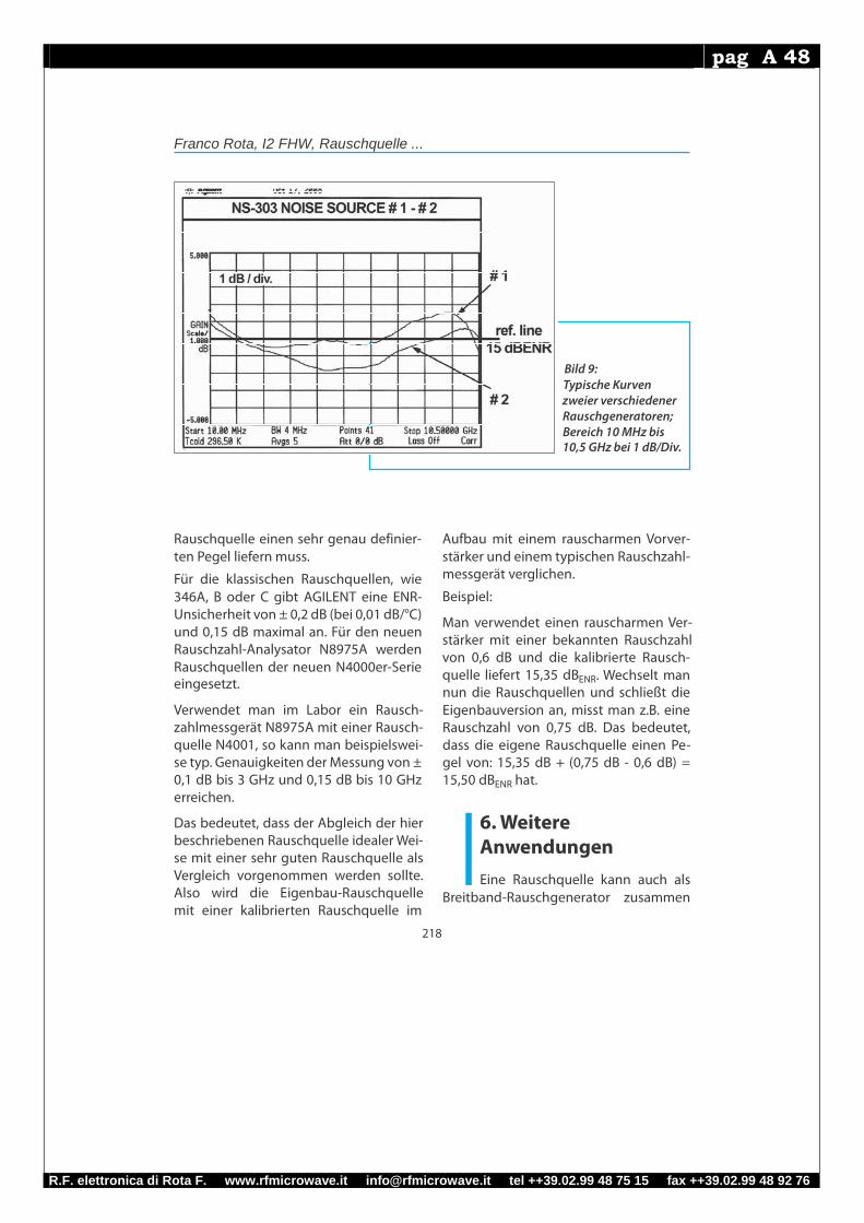
R.F. elettronica di Rota F. www.rfmicrowave.it [email protected] tel ++39.02.99 48 75 15 fax ++39.02.99 48 92 76
pag A 48
I
Franco Rota, I2 FHW, Rauschquelle ...
Bild 9: Typische Kurven zweier verschiedener Rauschgeneratoren; Bereich 10 MHz bis 10,5 GHz bei 1 dB/Div.
Rauschquelle einen sehr genau definier- ten Pegel liefern muss.
Für die klassischen Rauschquellen, wie 346A, B oder C gibt AGILENT eine ENR- Unsicherheit von ± 0,2 dB (bei 0,01 dB/°C) und 0,15 dB maximal an. Für den neuen Rauschzahl-Analysator N8975A werden
Aufbau mit einem rauscharmen Vorver- stärker und einem typischen Rauschzahl- messgerät verglichen.
Beispiel:
Man verwendet einen rauscharmen Ver- stärker mit einer bekannten Rauschzahl von 0,6 dB und die kalibrierte Rausch-
Rauschquellen der neuen N4000er-Serie eingesetzt.
quelle liefert 15,35 dB ENR. Wechselt man
Verwendet man im Labor ein Rausch- zahlmessgerät N8975A mit einer Rausch- quelle N4001, so kann man beispielswei- se typ. Genauigkeiten der Messung von ± 0,1 dB bis 3 GHz und 0,15 dB bis 10 GHz erreichen.
Das bedeutet, dass der Abgleich der hier beschriebenen Rauschquelle idealer Wei- se mit einer sehr guten Rauschquelle als Vergleich vorgenommen werden sollte. Also wird die Eigenbau-Rauschquelle mit einer kalibrierten Rauschquelle im
218
nun die Rauschquellen und schließt die Eigenbauversion an, misst man z.B. eine Rauschzahl von 0,75 dB. Das bedeutet, dass die eigene Rauschquelle einen Pe- gel von: 15,35 dB + (0,75 dB - 0,6 dB) = 15,50 dBENR hat.
6. Weitere Anwendungen
Eine Rauschquelle kann auch als
Breitband-Rauschgenerator zusammen
R.F. elettronica di Rota F. www.rfmicrowave.it [email protected] tel ++39.02.99 48 75 15 fax ++39.02.99 48 92 76
pag A 49
IUKW-Berichte 4/2008
mit einem Spektrum-Analysator wie ein „Tracking-Generator“ für skalare Anwen- dungen eingesetzt werden.
Natürlich ist das kein echter „Tacking- Generator“, weil er ja ganz anders arbei- tet. Das Problem liegt einfach darin, dass man einen Frequenzbereich über 3 Deka- den erreichen sollte, also von 10 MHz bis 10 GHz mit einem linearen Verstärker mit mindestens 50 dB Verstärkung!
Es gibt heutzutage entsprechende MMICs, die hierfür geeignet wären, wie die Typen ERA-1, ERA-2, MGA 86576 u.s.w. Problematisch ist jedoch, eine sehr flache Verstärkungskurve über den gro- ßen Frequenzbereich zu erhalten und die Schwingneigung bei so hohen Verstär- kungen zu verhindern.
So eine Baugruppe kann natürlich ein sehr nützliches Hilfsmittel für die unter- schiedlichsten Messaufgaben sein. Es kann beim Filterabgleich mit Spektrum- analysatoren eingesetzt werden oder zur Messung der Rückflussdämpfung - und das bis 10 GHz.
7. Literaturhinweise
Nachfolgend noch Links und Lite- raturhinweise zum Artikel: [1] VHF-Communications 1/2007 „Noise source diodes“
[2] For those who need more information about the mismatch uncertainty in noise figure measurement I suggest 3 applica- tion notes: - Ham Radio, August 1978, - Noise figure measurement accuracy
AN57-2 Agilent, - Calculating mismatch uncertainty,
Microwave Journal May 2008
[3] R.F. Elettronica web site cataloque www.rfmicrowave.it (capacitors section) [4] VHF-Communications 4/2004 „Franco´s finest microwave absorber“
Übersetzung Englisch - Deutsch: Eberhard L. Smolka, DB 7 UP
ANZEIGE
219