schottky barrier diode fabrication on n-gan for
TRANSCRIPT

Schottky barrier diode fabrication on n-GaN for
ultraviolet detection
by
Mmantsae Moche Diale
Submitted in partial fulfillment of the requirements for the degree
PHILOSOPHIAE DOCTOR
In the Faculty of Natural & Agricultural Sciences
Department of Physics
University of Pretoria
PRETORIA
September 2009
Supervisor: Prof. F. D. Auret
©© UUnniivveerrssiittyy ooff PPrreettoorriiaa

ii
TO MY SON
LEBOGANG ONKGOPOTSE
DIALE

iii
Brain Child

ACKNOWLEDGMENTS
The opportunity to be at one of the foremost research universities in the world and pioneer GaN
research in South Africa is one I will always be grateful for, and there are many people who have
inspired, guided and assisted me. I want to thank my supervisor, Professor F. Danie Auret, for
accepting me as his student. Thank you for all your support and guidance during my time at the
University of Pretoria. It has been both an educational and an emotional experience to work with
the Thin Films and Electronic Materials group. The atmosphere was not always enjoyable, but
the willingness to learn and apply emotional intelligence has helped me to pull through. I thank
Andre Botha and all the members of the microscopy unit for their helpful discussions that led to
my first presentation at an international conference as regards this thesis. I wish to express
special thanks to Professor Johan Brink for helpful discussions and advice in the experiments
that involved the use of optical equipment. I wish to thank Professor Johan Malherbe, the head of
the Department of Physics, for his encouragement and interventions during difficult times. I am
so glad to have shared this experience with my fellow students in this Department. Gunther
Kassier was the first student who worked very closely with me in the endeavour to set-up the
optoelectronic station, which was finalized by Louwrens van Schalkwyk. Special thanks to my
fellow students and colleagues for answering important questions of the moment: Hannes de
Meyer, Machesa Legodi, Claudia Zander, Johan Janse van Rensburg, Sergio Coelho, Cloud
Nyamhere, Wilbert Matangi, Albert Chawanda, Rik van Laarhoven, Quinton Odendaal, Walter
Meyer, and Augusto Machatine.
Finally I thank my husband Dr OPPP Diale for financial and emotional support.
The financial support of the project stemmed from the National Research Foundation and the
University of Pretoria.
v
Schottky barrier diode fabrication on n-GaN for
ultraviolet detection
by
Mmantsae Moche Diale
Submitted in partial fulfillment for the degree PhD (Physics) in the Faculty of Natural and
Agricultural Science, University of Pretoria
Supervisor: Prof. F. D. Auret
There are many potential areas for the utilization of GaN-based nitride materials, including
ultraviolet photodetectors. Ultraviolet photodetectors are used in the military for missile plume
detection and space communications. Medically, ultraviolet photodiodes are used in monitoring
skin cancer. Schottky barrier metal-semiconductor contacts are choice devices for the
manufacture of ultraviolet photodiodes due to higher short wavelength sensitivity and fast
response. They also require simple fabrication technology; suffer lower breakdown voltages, and
record larger leakage currents at lower voltages as compared to p-n structures of the same
semiconductor material. Thus the formation of a Schottky contact with high barrier height, low
leakage current, and good thermal stability in order to withstand high temperature processing and
operation are some of the most important factors in improving the performance of Schottky
barrier photodiodes to be used for ultraviolet detection. The first stage of this study was to
establish a chemical cleaning and etching technique. It was found that KOH was suitable in
reducing C from the surface and that (NH4)2S further reduced the surface oxides. The next phase
of the work was to select a metal that will allow UV light to pass through at a high transmission
percentage: a combination of annealed Ni/Au was found to be ideal. The transmission percentage
of this alloy was found to be above 80%. The next phase was the fabrication of Ni/Au Schottky
barrier diodes on GaN to study the electrical characteristics of the diodes. Electrical

vi
characterization of the diodes showed that the dominant current transport mechanism was
thermionic emission, masked by the effects of series resistance, which resulted from the
condition of the GaN surface. Finally, we fabricated GaN UV photodiodes and characterized
them in the optoelectronic station designed and produced during this research. Device
responsivity as high as 31.8 mA/W for GaN and 3.8 mA/W for AlGaN were recorded. The
calculated quantum efficiencies of the photodiodes were 11 % for GaN and 1.7 % for AlGaN
respectively
Keywords: Al(GaN), Schottky, photodiodes, Ultraviolet, responsivity, quantum efficiency.

vii
TABLE OF CONTENTS
ACKNOWLEDGEMENTS iv
ABSTRACT v
1 Introduction 1 1.1 Introduction 1
1.2 Aims of the study . 6
1.3 Synopsis of thesis 6
References 7
2 GaN-based materials for Ultraviolet detectors 8
2.1 Introduction 8
2.2 Progressive development of GaN 8
2.2.1 Growth Methods 9
2.2.2 Substrates to GaN 12
2.2.3 High n-type conductivity 13
2.2.4 Doping of GaN 14
2.2.5 Effects of defects on GaN devices 15
2.3 Properties of GaN-based materials 16
2.4 Applications of GaN 19
2.5 AlGaN photodetectors 21
2.6 Ohmic contacts to AlGaN 22
References 24
3. Schottky Barrier Ultraviolet Photodetectors 31 3.1 Introduction 31
3.2 Ultraviolet photodetectors 31
3.2.1 Active area of semiconductor diode 33
3.2.2 Responsivity 33
3.2.3 Operation Voltage 35
3.2.4 Dark current-voltage characteristics 35
3.2.5 Response speed 36
3.2.6 Capacitance 37
3.2.7 Series resistance 37
3.3 Schottky-Mott theory and its modifications 38
3.4 Current transport mechanisms 41
3.5 Theory of ultraviolet photodetectors 43
References 45

viii
4 Experimental Techniques 47 4.1 Introduction 47
4.2 Sample preparation 47
4.3 Surface characterization 48
4.3.1 Auger Electron Spectroscopy 48
4.3.2 Scanning Electron Microscopy 49
4.3.3 Atomic Force Microscopy 50
4.4 Electrical and Optical Characterization 51
References 55
EXPERIMENTAL RESULTS 56
5 Analysis of GaN Cleaning procedures 57 5.1 Introduction 57
5.2 Experimental 60
5.3 Results and Discussion 63
5.3.1 Atomic Force Microscopy 63
5.3.2 Auger Electron Spectroscopy 75
5.4 Conclusions 78
References 80
6 Study of metal contacts on GaN for transmission of UV light 81 6.1 Introduction 81
6.2 Choice of metal for transparent contacts 82
6.3 Experimental 83
6.4 Results and Discussion 83
6.5 Conclusions 90
References 91
7 Chemical treatment effect on Au/GaN diodes 92
7.1 Introduction 92
7.2 Experimental 94
7.3 Results and Discussion 94
7.3.1 Capacitance-Voltage 94
7.3.2 Current-Voltage 96
7.4 Conclusions 99
References 100

ix
8 Fabrication of GaN/AlGaN Schottky barrier photodiodes 101 8.1 Introduction 102
8.2 Experimental 103
8.3 Results and Discussion 104
8.4 Conclusions 111
References 112
9 Conclusions 113
List of Publications 116

1
CHAPTER 1
1.1 Introduction
The ultraviolet (UV) region of electromagnetic radiation occupies a section of wavelengths
ranging from 400 to 10 nm [1]. It is highly ionizing and activates many chemical processes on
different types of materials and living beings. It is divided into four categories: near UV with
wavelength range 400 to 300 nm, middle UV from 300 to 200 nm, far or vacuum UV from 200
to 100 nm and extreme UV from 100 to 10 nm. The lower wavelength radiation that generally
reaches the earth’s surface is the first mentioned. Middle UV radiation is absorbed by the ozone
layer while far UV radiation is absorbed by molecular oxygen. Extreme UV radiation is absorbed
by all types of atomic and molecular gases and is not supposed to reach the earth’s surface at all.
As a function of its effects on the biosphere, the UV regions are arbitrarily called: UVA from
400–320 nm, UVB from 320-280 nm and UVC from 280-180 nm [2]. The different regions for
the UV section of the electromagnetic spectrum are shown in Table 1.1 below.
Table 1.1: UV radiation wavelength range and corresponding names [2].

2
Further classification of the radiation wavelength is termed the solar-blind and visible blind
regions. Some UV radiation from the sun is absorbed by the ozone in a certain range of
wavelengths, thus not reaching the earth’s atmosphere. Figure 1.1 indicates this condition with a
comparison between the regions above and below the atmosphere. Some detectors require that
the UV signal be detected in the background of the sun. It is evident from the figure that the
amount of solar radiation reaching the earth’s surface drops greatly around 300 nm (4.1 eV).
Thus a solar blind detector detects UV radiation below 300 nm. The wavelength range of AlGaN
makes it possible to have both visible-blind and solar blind UV detectors, depending on the
energy of the radiation to be detected.
Figure 1.1: Solar UV above and below the atmosphere of the earth, from 1976 US standard
atmosphere [3].

3
In addition, figure 1.2 clearly depicts the solar blind and visible blind regions. Visible blind
indicates those regions where UVB radiation is active while solar blind refers to the regions
where UVC is dominant. UVB never reach the earth surface in general, but due to ozone layer
depletion, there may be some effects of on the biosphere.
Figure 1.2: Regions of electromagnetic radiation, showing the different ultraviolet sections
and their borders [4].
The main source of UV radiation is the sun. The energy per unit of time reaching the earth at
right angles to the light rays that are observed outside the earth’s atmosphere is 1353 W/m2, of
which only 121.8 W/m2
(9%) constitute the total UV radiation [4]. The UV radiation on earth
and its effects depend on the solar altitude angle lying between any line directed to the sun and
the projection on the horizontal plane. Thus the amount of UV radiation at different places on the
earth depends on the position of the sun during the day and the season of year. Research in
Germany has shown that a decline in the amount of ozone has been observed to be high in
spring, indicating an increase in UV radiation at that time of the year [5]. UV radiation is also
produced artificially from electroluminiscence of certain types of matter, when ions, atoms and
molecules are accelerated at high voltages.
A global scale called Solar Ultra Violet Index (UVI) is used to describe the level of UV radiation
on the biosphere; it is usually seen on TV during the weather forecast. The UVI is a form of

4
warning to mankind to protect oneself against such a radiation effect. The values range from zero
to ten and above, indicating the strength of UV radiation. These values depend on the
geographical region and time of day [6]. In many places, the UVI is very high around midday
and it is required that one must be protected from the effects of the sun. When the UVI is less
than three, a person may be free from these harmful effects, but anything above this calls for
protection.
The effects of UV radiation on the biosphere lead to issues such as sunburn, skin cancer and eye
cataracts. Sunscreens, hats and sunglasses are used together for maximum protection from UV
radiation. Issues with regards to these protection systems include the correct amount of sunscreen
protection, known as the Sun Protection Factor (SPF), in the solutions that are applied. The
values differ from skin to skin and from person to person. A common practice amongst some fair
skinned people is to expose themselves to UV radiation in order to pigment their skin.
Overexposure may lead to erythema and premature aging, which may be followed by skin cancer
and eye cataracts [7]. Snow, white sand, water and any similar substances increase one’s UV
exposure by reflection and this is not good for one’s eyes.
However, UV radiation effects are beneficial to humankind well being in terms of the activation
of vitamin D, the most important of sun energy and stimulation of photosynthesis [8].
Sterilization of water and the removal of micro-organisms from foods and in the pasteurization
process require the use of UV radiation. Such radiation is used in modern refrigeration to keep
food and air free of micro-organisms during long storage, giving them longer life. In
biotechnology, UV radiation is used in the synthesis of vitamins D2 and D3. In addition, UV
flytraps are used to control pests, killing them through shock once attracted to the light.
UV detection has been achieved by photomultiplier tubes (PMT), thermal detectors, and
charged-coupled devices (CCD). PMT displays high gain and low noise and can reduce the
infiltration of low energy photons, but these are large fragile instruments that require much
power. Thermal detectors such as pyrometers and bolometers are used in the calibration
processes of UV detectors, but are slow and their response is wavelength independent.
Semiconductor photodiodes and CCDs are narrow bandgap solid-state devices that require

5
moderate bias. As solid-state devices, photodetectors are small, lightweight and insensitive to
magnetic fields. Their low-cost, good linearity and sensibility, and capability of high-speed
operation make them suitable for UV detection. Si, GaAs, and GaP have been used in the
fabrication of UV detectors [9]. These materials are suitable for devices operating in the visible
and infrared sections of the electromagnetic radiation. UV detectors made from these materials
need filters to stop interference of low energy radiation.
The most common semiconductor UV enhanced devices are made of Si, displaying some
limitations due to the narrow and indirect bandgap of Si. Si-based UV photodiodes have been
made as p-n junction photodiodes and charge inversion photodiodes. In p-n-junction UV
photodiodes, the junction is typically situated at a depth of 0.2 µm and the devices are coated
with a SiO2 surface layer, acting as surface passivation and anti-reflection coating [10]. The
charge inversion photodiodes are similar to metal-oxide semiconductor structures designed for
field effect transistors. Photodetection occurs as a result of the presence of the electric field at the
Si/SiO2 interface. This is the region of high UV radiation absorption and requires control of the
surface recombination at the Si/SiO2 interface, which is very critical for the performance of the
device. Si, GaP, CsI and GaAs-based UV detectors suffer radiation aging, as their bandgap is far
lower than the UV photon energies.
Diamond, SiC, GaN and ZnO are wide bandgap (WBG) semiconductors suitable for the
fabrication of UV detectors [11]. The wide bandgap is itself an important advantage for UV
detectors because it enables room-temperature operation and provides important intrinsic visible
blindness. Thermal conductivity of the wide bandgap materials is very high compared to that of
Si, which renders devices suitable to operate in high temperature and high power environments.
Electron velocities of the WBG semiconductors are lower than those of conventional
semiconductors, but at high electric fields, these become larger. A further interesting feature of
WBG semiconductors for operation in the lower wavelengths of the electromagnetic spectrum is
the ability to display negative electron affinity [12], which makes electrons readily available
when the semiconductor interacts with appropriate photon energies. In this thesis, GaN-based
materials are used in the study of ultraviolet detectors.
6
1.2 Aims of the study
In this work, the focus falls on the optimization of Schottky diodes suitable for use as UV
detectors on GaN-based semiconductors. The performance of metal contacts on semiconductors
depends on the quality of the surface prior to metallization, the chemicals used in preparing the
surface, the morphology of the surface, the adhesion of the metal to the semiconductor,
reproducibility, resistance to radiation damage and thermal stability. The aims of the study were
to establish the following:
Cleaning procedures for GaN for the purpose of metallization.
GaN for device patterning using wet etch processes.
Choosing a metal contact with high UV light transmission.
Fabrication of Schottky barrier UV detectors.
Setting-up an electro-optical characterization station for the evaluation of the
UV detectors.
1.3 Synopsis of the thesis
The focus of this work has been described. This chapter serves as a prelude to the GaN
UV detectors and offers the motivation for the study. Chapter 2 consists of the literature
review on GaN semiconductors for UV detectors. Chapter 3 presents a theoretical
overview of Schottky Barrier diodes, while Chapter 4 contains the experimental details of
the research. Chapter 5 furnishes the results of all experiments and Chapter 6 presents the
conclusions.

7
REFERENCES
[1] Razeghi M. and Rogalski A., Journal of Applied Physics 79 (1996) 7433.
[2] Goldberg Y. A., Semiconductor Science and Technology, 14 (1999), R41.
[3] Parish G., PhD Thesis, University of Santa Barbara (2001)
[4] Coulson K. L, Solar and Terrestrial Radiation, Academic Press, New York (1975).
[5] Winkler P. and Trepte S., Gesundhetswesen, Suppl. 66 (2004) S31.
[6] Koepke P., De Backer H., Ericson P., Feister U., Grifoni D., Koskela T., Lehman A.,
Lityska Z., Oppenrieder A., Staiger H. and Vanicek K., UV Index Photobiology,
International Radiation Symposium (2000).
[7] Mackie R. M., Progress in Biophysics and Molecular Biology, 92 (2006) 92.
[8] Schmalwieser A. W. and Schauberger G., ICB2005, Garmisch-Partenkirchen, Germany
[9] Rogalski A., Progress in Quantum Electronics 27 (2003) 59.
[10] Korde R. and Geist J., Applied Optics 26 (1987) 5284.
[11] Monroy E., Omness F. and Calle F., Semiconductor Science and Technology 18 (2003)
R33.
[12] Nemanich R. J., English S. L., Hartman J. D., Sowers A. T., Ward B. L., Ade H. and
Davies R. F., Applied Surface Science 146 (1999) 287.

8
CHAPTER 2
GaN-based materials for Ultraviolet
Detectors
2.1 Introduction
In this chapter, the basic information about GaN-based materials is presented. The issues that
affected the development of GaN are discussed in section 2.2. This is followed by a discussion of
the properties and applications of GaN-based materials. Finally, a review of AlGaN photodiodes
is done.
2.2 Progressive development of GaN-based materials
GaN is one of the most successful materials used to make optoelectronic devices operating in the
blue and ultraviolet region (UV) of the electromagnetic spectrum. Most colours in the visible
range have been covered by other semiconductors with Si and GaP containing devices operating
in the infrared (IR) region. Since the 1990s, there has been notable growth in the research and
development of GaN devices [1]. However, the success of such devices has been limited by
material issues such as the presence of high-unintended donor concentrations [2], lack of suitable
substrates [3] and growth methods. These issues resulted in dislocation densities as high as 1 x
1010
cm-2
, leading to uncontrollable electronic properties in GaN crystals [4,5]. Similarly, AlN
and InN suffered in the same manner in their development, and both are useful in bandgap
engineering, producing AlGaN and InGaN respectively. In and Al content in GaN can be tailored
to select a specific wavelength for device fabrication [6]. InGaN and AlGaN are used to
introduce green and UV wavelengths respectively. Figure 2.1 presents a graph of bandgap tuning
with Al and In in GaN. SiC, diamond, and ZnO are inserted for comparison.

9
Figure 2.1: Bandgap of GaN-based materials for UV detectors. SiC, ZnO and diamond are
inserted for comparison.
2.2.1 Growth methods
In an effort to improve the quality of GaN crystals and reduce dislocation density, several growth
methods were used. The growth methods that have been used are vapour phase epitaxy (VPE),
which includes both hydride (HVPE) [7] and metal organic vapour phase epitaxy (MOVPE) [8],
and molecular beam epitaxy (MBE) [9]. MOVPE is a chemical vapour deposition method, also
termed metal organic chemical vapour deposition (MOCVD), organometallic chemical vapour
deposition (OMCVD) or organometallic vapour phase epitaxy (OMVPE). This method uses
ammonia (NH3) and trimethyllgallium (TMG) as precursors for nitrogen and gallium,
respectively. In the case of other nitrides, trimethyllaluminium (TMAl) and trimethylinduim
(TMIn) are used as sources for Al in AlN and In in InN, respectively. The chemical equation for
the growth of GaN is given by:

10
3 3 3 4( )Ga CH NH GaN CH (2.1)
The MOCVD method requires a high partial pressure for NH3 and a high growth temperature,
ranging from 1000 to 1100°C. The first step is growing the material at low temperature
producing GaN crystallites that covers the substrate. The final film is grown at a higher
temperature to control and reduce contamination in the material. GaN is doped with Si or Mg for
n-type and p-type doping. In n-type doping, Si is sourced from methyl silane, while in p-type
doping Mg is sourced from biscyclopentadithyl. Figure 2.2 shows the growth process of the III-
Nitrides. The carrier gas introduces the required element for the growth of GaN and the by
products are expelled from the system, with the semiconductor growing onto a substrate.
Figure 2.2: MOCVD growth process for III-Nitrides.
MBE is an ultra high vacuum technique for growing semiconductor crystals. High purity Ga is
heated in an effusion cell until it evaporates and deposits slowly onto a substrate. Nitrogen atoms
are supplied from a plasma source. The growth of GaN is controlled by conditions that allow

11
atoms of Ga and N to be deposited layer by layer onto a heated substrate. The MBE method
operates in an ultra high vacuum chamber to minimize crystal contamination during growth. This
method is capable of producing heterostructures with sharp interfaces and of growing
zinc-blende structure GaN (normally, GaN is grown in a wurtzite structure). The chamber is also
equipped with Si, Mg, In and Al effusion cells for alloying purposes. The disadvantage of the
MBE method is the low growth temperature, 700 to 800°C as compared to MOCVD where
temperatures are 1000 to 1100°C. GaN is a thermodynamically unstable material in a vacuum
and the thin film may decompose into Ga and N in the MBE, when the deposition rate becomes
lower than the decomposition rate due to a temperature difference between the chamber and the
substrate. The low substrate temperature reduces surface atom mobility, resulting in increased
densities of defects [10]. Figure 2.3 shows the schematics of the MBE growth method.
Figure 2.3: MBE growth process for III-Nitrides [11].
12
2.2.2 Substrates for GaN
In addition to the growth method, the crystal quality of semiconductors depends on the suitability
of the substrate. In growing GaN, sapphire (α-Al2O3), GaAs, Si, SiC, LiGaO2, LiAlO2 and ZnO
have been used as a substrate [3]. The criterion for choosing a suitable substrate is lattices match.
In addition, practical properties such as crystal structure, surface finish and composition,
chemical, thermal and electrical properties are also considered. Currently, it has become
important to study the effects of treatments of a substrate (e.g. heating or chemical processing)
prior to the deposition of GaN. For example, it has been shown that wet etching of sapphire prior
to the deposition of GaN crystals reduces threading dislocations [12]. α-Al2O3 has been
extensively used as a substrate for GaN. It has a crystal orientation parallel to GaN c-plane, and
the lattice mismatch is about 15 %, leading to a dislocation density of about 1010
cm-2
. α-Al2O3
has a rhombohedral structure and is highly anisotropic. Like GaN, it exhibits extremely high
chemical and thermal stability with a melting point of 2040 °C. Its bandgap of 9.1 eV permits
excellent optical transmission. Furthermore, the coefficient of the thermal expansion of α-Al2O3
is greater than that of GaN, resulting in comprehensive stress in the grown film during cooling.
Such stress causes cracks in both GaN and α-Al2O3.
A continually improving technique to produce GaN with less threading dislocations is the
epitaxial lateral overgrowth (ELOG), considered to be an alternative substrate [13]. Figure 2.4
depicts the schematics of the ELOG substrate. The ELOG technique takes advantage of the large
anisotropy of the GaN growth rate in the [0001] direction, controlling dislocations through the
patterned substrate such that they do not reach the surface of the final layer as shown in figure
2.4 (D). GaN thin buffer layer is grown on sapphire as a usual practice for GaN growth as shown
in figure 2.4 (A). A dielectric material such as SiO2 or SiN mask is then patterned onto the GaN
buffer layer figure 2.4 (B). The thin film is then grown onto the patterned GaN buffer layer
figure 2.4 (C). Using MOCVD, ELOG and several of its variations has been shown to
significantly reduce the dislocation density of GaN crystals to as low as 106 cm
–3 [14].

13
Figure 2.4: Schematic representations of 2 step ELOG for GaN, where NL is the GaN
nucleation layer [13].
2.2.3 High n-type Conductivity
The first GaN crystals were observed to possess high n-type conductivity, which was attributed
to nitrogen vacancies. This is an unresolved issue in GaN research. Published reports
[15,16,17,18] suggest impurities such as Si, C, O, and H as being responsible for n-type
conductivity. Park et al. have reported that Si and C are responsible for n-type doping in GaN
films [15], where C atoms are acting as compensating acceptors in the crystal, influencing the
electron concentration. Van de Walle et al. reported that O, a shallow donor in GaN, is
responsible for high background n-type conductivity while Zhang et al. claim that H is
responsible for this phenomenon [16,17]. In addition to n-type conductivity, there is a strong
presence of parasitic yellow band (YB) luminescence associated with point defects in GaN
crystals. Ogino et al. suggested that the YB is a transition that takes place between a shallow
donor and a deep accepter level [18]. This suggestion was demonstrated by Saarinen et al. using
14
positron annihilation spectroscopy, and they concluded that the intensity of YB is directly
proportional to the concentration of Ga vacancies [19]. Reynolds et al. have studied the source
of yellow luminescence in GaN. They concluded that Ga vacancies, in partnership with the O
atom at a nitrogen site, are responsible for point defects producing the YB [20]. More recently,
researchers have again suggested that the YB is associated with O impurities in GaN [21].
Related to the impurities discussed above, defects have been studied using Deep Level Transient
Spectroscopy (DLTS), which identified vacancies and interstitials in semiconductors. Defects in
materials act as electron and hole traps, affecting the current transport in devices. In HVPE
grown GaN, three electron traps have been shown by DLTS: E1, E2 and E3 with activation
energies 0.264, 0.580 and 0.665 eV [22], with E1 and E2 appearing in concentrations above 2 X
1013
cm-3
in MOVPE [23]. Auret et. al. have also reported two electron traps, Ec - 0.23 eV and
Ec - 0.58 eV, in non-intentionally doped MOVPE GaN with activation energies 0.27 and 0.61 eV
[24].
2.2.4 Doping of GaN
Doping of GaN plays a crucial role in the performance of devices as it alters GaN’s electrical
properties by enhancing its conductivity. Using Si in n-type doping of GaN, a carrier density as
high as 2.2 x 10¹⁹
cm-3
and a Hall mobility of 287 cm2/Vs have been recorded [25]. In addition,
Si doping has led to a reduction of threading dislocation density in GaN, through the formation
of SiN, which stops the propagation of edge dislocation from reaching the surface of the
crystal.]. In the case of p-type doping, group II elements like Mg, Be, Ca, Zn, and a combination
of Mg and Be have been used. Mg doping is the most efficient, allowing the production of semi-
insulating p-type crystals. The highest carrier density in Mg doped GaN has been recorded as 8 x
1018
cm-3
with the correspondingly low resistivity of 0.8 Ω cm. For p-GaN growth with Ga-
polarity, the incorporation of Mg has a tendency to introduce stacking faults, thus inverting the
polarity to N-face, and reducing threading dislocation from reaching the surface [26]. These are
also defects introduced into the material which exert adverse effects on the performance of
devices.

15
2.2.5 Effects of defects in GaN devices
GaN, like all semiconductors, contains defects due to growth conditions, method of growth,
doping, and the substrate used. Dislocations are observed directly from the substrate where the
growth begins from a low temperature nucleation layer. Growth processes with both the
continuous nucleation layer and the one formed by isolated islands end with vertical threading
dislocations. Dislocations in GaN are identified as edge-type, screw type and mixed character
type. All these defects influence device performance, including the different types of
photodiodes. GaN photodiodes are characterized by high gain, long response time and a
responsivity that is dependent on frequency and optical power. Gain is defined as the ratio of the
excess–carrier recombination lifetime and the electron transit time across the diode. Since
electrons have very high mobility in GaN, high gain will be affected by a long stay of carriers in
traps, reducing the probability of recombination. High gain thus occurs at the expense of the long
response time of minority carriers. Published works have attributed the mechanism of the long
response times and high gain in n-type GaN photoconductors to acceptor levels trapping the
photogenerated holes [27, 28, 29]. Traps in the semiconductor material occur as a result of both
point defects and dislocations. Hole traps can be reduced by altering the growth conditions for
GaN-based materials, and this has proved to have an effect on the photoresponse [30]. Leakage
currents in photodiodes consist of the dark current at the reverse bias and have different sources.
Surface leakage currents result from surface states and tunneling induced near the surface, and is
reduced by surface chemical treatments including passivation. Passivation is responsible for
tying up dangling bonds and thus reduces the density of surface states. Reduced leakage currents
have been reported in devices grown on ELOG GaN p-n structures and Schottky photodiodes,
which are characterized by reduced threading dislocation densities [31]. Low leakage current
improves the response time and sharpness of the cut-off wavelength in ELOG GaN [32].

16
2.3 Properties of GaN-based materials
GaN, with its famous nitride family, AlN and InN, are wide band gap semiconductors that occur
in both zincblende and wurtzite structures. Figure 2.5 shows the schematics of GaN wurtzite
structure, showing the Ga-face and the n-face. In wurtzite form, the direct band gap of GaN is
recorded at 3.5 eV while that of AlN is 6.23 eV [33]. The bandgap of InN was recorded earlier as
1.9 to 2.05 eV [34] while more recently, a new band gap of 0.7 to 1.0 eV [35] was recorded. In
cubic form the bandgaps of GaN and AlN are direct while that of InN is indirect [36]. Alloying
GaN with InN and AlN allows for the tuning of band gaps and emission wavelengths. AlGaN is
suitable for the fabrication of UV solar-blind detectors. By varying the Al content, the
responsivity cut-off wavelength can be varied from 280 nm [37] to as low as 240 nm [38].
Figure 2.5: Schematic representations of wurtzite GaN, where Ga-face and N-face are
indicated by opposite directions [39].

17
GaN based materials possess excellent transport properties suitable for high power, high
temperature and high frequency devices. The electron saturation velocity of GaN is
2.5 x 107 cm.s
-1 at a field 10
5 Vcm
-1 [40]. The electron mobility of epitaxial GaN has been
recorded at 1000 cm2V
-1s
-1 for epitaxial layers [41,42]. The value of low temperature mobility in
doped GaN is recorded above 7000 cm2V
-1s
-1 [43]. GaN based materials have high breakdown
fields of up to 5 x 10⁶
V-1
cm-1
[44]. SiC is one wide bandgap semiconductor that possesses a
higher thermal conductivity than GaN, which makes it superior to GaN for high temperature
devices. However, GaN, with a thermal conductivity greater than 2.1 Wcm-1
°C-1
, enjoys the
direct bandgap advantage [45].
The wurtzite (hexagonal) structure GaN based materials are grown along the [0001] direction
while the zincblende (cubic) crystals are grown along the [1111] direction, as shown in
figure 2.5. These are polar axes, which cause GaN-based semiconductors to contain strong lattice
polarization effects. Large spontaneous polarization is suitable for applications in high
temperature piezoelectronics and in pyroelectronic sensors. Properties such as piezoelectricity
and pyroelectricity are important elements in detector technology. Piezoelectric semiconductors
are able to generate electric potentials in response to applied mechanical stress, while
pyroelectric materials are capable of generating electric charges in response to heat flow. When
heat is applied it changes the temperature of the material by means of thermal convection,
diffusion or radiation. GaN and AlN are believed to contain some spontaneous polarization,
leading to high piezoelectric constants, which furthermore leads to high piezoelectric
polarization in strained films [46].
The pyroelectric response in GaN-based materials results from the piezoelectric effects of
temperature-induced strain. There exists a primary piezoelectric effect, which is dominant during
fast heat transfer such as the immersion of a device in a medium with high flow velocity. In such
a medium, a GaN-based sensor generates a response voltage that is proportional to heat flow. For
example, there is a difference in the thermal expansion coefficients of the substrate and the
pyroelectric material produces strain in response to temperature changes owing to the applied
strain (piezoelectric strain), which in turn generates an electric charge [47]. It has been shown
that the pyroelectric voltage coefficient in GaN can be as high as 7 x 10⁵
V/m-K [48] and is

18
higher than that of the best-known high temperature pyroelectric material, LiTaO3, whose
pyroelectric voltage is 5 x 10⁵
V/m-K [49]. In GaN based materials, strong polarization effects
result from piezoelectric polarization, which depends on the lattice strain and spontaneous
polarization. Spontaneous polarization exerts a strong influence on the electrical properties of
heterostructures such as the electron density. Spontaneous polarization arises as a result of large
ionicity associated with covalent metal nitrogen bonds and low symmetry in wurtzite material. It
also causes an unstable electric field that may decrease or increase the interfacial carrier
concentration. In heterostructures where strain is present, the polarization charge is inextricably
connected to the present free carriers in the semiconductor. The magnitude of this charge is
measured by converting it to the number of electrons: it can be in the mid 1013
cm-2
level for
AlN/GaN interfaces [46]. This is very high compared to AlAs/GaAs heterostructures, where the
number of electrons is less than 10% of that of the AlN/GaN structure. AlGaN/GaN devices, in
particular, high-electron-mobility-transistor (HEMT), have an extremely large charge density as
a result of the two dimensional electron gas (2DEG) formed at the AlGaN/GaN interface,
occurring even without doping in the AlGaN. Figure 2.6 shows the energy band of a basic
HEMT, indicating the position of 2DEG. Table 2.1 furnishes a summary of some of the
properties of III-nitride semiconductors.
Figure 2.6: AlGaN/GaN structure showing the 2DEG caused by spontaneous and
piezoelectric polarization [50].

19
Table 2.1: Properties of Wurtzite III-Nitrides Semiconductors.
2.4 Applications of GaN-based materials.
III-nitrides are suitable semiconductor materials for use in optoelectronic devices, as both
emitters and detectors. They can also be used to fabricate high power and high temperature
electronic devices [51]. The allowed energy bandgaps of these materials are suitable for band-to-
band light generation with colours ranging from potentially red to UV wavelengths, rendering
them an advantageous addition to the already existing semiconductor systems for colour
displays. It has been demonstrated that nitrides can be used as Bragg reflectors [52], UV
detectors [53], UV and visible light emitting diodes (LEDs) for applications in flat panel
displays, lighting and indicator lights on devices, advertisements and traffic signals [54]. As
coherent sources, lasers are important for high-density optical read-write technologies [55]. The
diffraction-limited optical storage density increases approximately quadratically as the probe
Property Units AlN GaN InN
Crystal Type Wurtzite Wurtzite Wurtzite
Energy Band Gap eV 6.2 3.39 1.89
Electron Mobility cm2/Vs 135 1000 (bulk) 1100
Hole Mobility cm2/Vs 15 30 10
Breakdown Fields V/cm 1.4 x 10⁵ >5 x 10
6 1.4 x 10
5
Saturation Velocity cm/s 1.4 x 10⁷ 2.5 x 10
7 2.5 x 10
5
Thermal Conductivity W/cmK 2 1.5 6.4 x 10⁻⁵
Lattice Constant, a Å 3.11 3.19 3.54
Lattice Constant, c Å 4.98 5.18 5.76

20
laser wavelength is reduced, making the GaN-based materials suitable for coherent sources at
lower wavelengths of the electromagnetic radiation. Optical storage enables the storage and
retrieval of data in vast quantities. Medical applications of UV LEDs and lasers include surgery
[56], phototherapy of neonatal jaundice [57], photodynamic therapy [30], photo-polymerization
of dental composites [30], phototherapy of seasonal affective disorder [30], and sterilization [58].
When used in surgery, UV lasers are seen as most suitable due to the fact that UV can sterilize.
In photosynthesis, the high brightness LEDs are suitable for the growing of plants and for photo
bioreactors [59]. Finally, the LEDs and laser diodes (LDs) are suitable for use in optical
measurements such as time domain and frequency domain spectroscopy [60]. Furthermore,
exposure to UV-B radiation causes skin cancer to fair skinned people. The use of AlGaN
ultraviolet detectors will help prevent such disease, where a handheld device will be able to
communicate to user how much ultraviolet radiation was absorbed.
There is great concern all over the world about the contribution of uncontrolled effluents to
global warming which is an unexpected change in climate. The effluents stem from aerosols, car
fumes, industries and wild fires, and add to the concentration of CO2 in the atmosphere. When
installed in jet engines, cars and furnaces, the UV detectors would monitor and control
contaminants for a cleaner environment. In addition, UV detectors operating in the solar-blind
region of the electromagnetic spectrum, when made from GaN-based materials, record a high
detectivity and are useful in the detection of UV-C (280 nm to 10 nm) and UV-B (320 nm to 280
nm) [61]. UV-C and UV-B are not detectable naturally because the ozone layer is a natural UV
filter for all radiation less than 280 nm [35]. It has been observed that power lines emit UV-C
radiation as a result of ionization of nitrogen around them.

21
2.5 AlxGaN1-x photodetectors
Since the first GaN UV photoconductive photodiode reported by Khan in 1992 [62], all types of
photodiode structures have been developed. These are linked directly with the advancement of
GaN and AlGaN growth, progress in p-type doping and the improvement of both ohmic and
Schottky contact technology. The first developments were focused on the fabrication of visible-
blind and solar-blind UV detectors in which the Al mole fraction plays a crucial role in
determining the detection band edge [63]. The next stages of development of the photodiodes
were focused on the advancement of detector parameters: high responsivity [64], high quantum
efficiency [65], high detectivity [66], and UV imaging using focal plane arrays [67].
Photoconductive photodiodes [68], p-n junctions [24], metal-semiconductor-metal (MSM) [69]
and Schottky barrier (SB) diodes [55] have already been reported. The success of Schottky
barrier photodetectors depends on the structure of both the metallization and the AlGaN used for
fabrication. Khan et al. reported the first high quality UV Schottky photodetectors. They used the
Cr/Au metal system for the preparation of the ohmic contacts and Ti/Au for Schottky barriers.
The spectral responsivity of these detectors reached a maximum value at 365 nm. Miyake et. al.
used a Ti/Al structure for the fabrication of ohmic contacts and Ni/Au for Schottky contacts. The
transmittance of the Ni/Au electrode in the near UV and VUV region was up to 60 %. The
responsivity of the AlGaN detector operating in the UV-VUV wavelength range was found to be
100-265 nm [53].
In recent advances, Tut et. al. demonstrated solar-blind photodetectors with low noise, high
detectivity and high quantum efficiency [70]. The AlGaN epitaxial layers were grown on
sapphire substrate using MOCVD. A thin nucleation layer of AlN was first deposited on
sapphire, to control the cracking of AlGaN. Unintentionally doped GaN mesa isolation with 0.5
μm thickness was grown onto AlN. This was followed by the deposition of a highly doped (2 x
1018
cm-3
; 0.6 μm) GaN ohmic contact layer. The diffusion barrier, expected to increase the solar
blindness of the photodetector, was deposited as a layer of 0.2 μm n-AlGaN. The growth of the
Schottky heterostructure was completed with the deposition of a 0.8 μm undoped AlGaN active
layer. Ti/Al (100 Å/ 1000 Å) ohmic contacts were deposited onto the highly doped GaN since it
was difficult to produce high quality ohmic contacts onto AlGaN. Au Schottky contacts of 100 Å

22
were deposited onto the active layer. The photodiodes exhibited a low leakage current: less than
3 fA and 10 fA for reverse bias voltages of 12 V and 17 V respectively. The spectral response of
solar blind photodetectors was measured at the 250 - 400 nm spectral range. When the applied
voltage increased from 5 V to 20 V, the peak responsivity increased from 61 mA/W at 250 nm to
147 mA/W at 256 nm. The responsivity reached saturation for voltages greater than 20 V,
indicating a total depletion of the undoped AlGaN absorption layer. A cut-off wavelength of the
diodes was reached at 267 nm, which ensures the true solar blindness operation of the diodes.
The zero-bias (photovoltaic) quantum efficiency was very low. A maximum quantum efficiency
of 71% was measured at 256 nm under 20 V reverse bias.
2.6 Ohmic contacts on AlGaN/GaN
Early studies of ohmic contacts on GaN used Al and Au metallization, which yielded specific
contact resistivities in the range of 10-4
and 10-3
Ωcm [71]. Addition of Ti/Au to Ti/Al improved
the specific contact resistivity to 10-6
Ωcm [72]. In taking the Ti/Al metal structure further, Wu et
al. confirmed that Ti/Al functions very effectively, except at a high annealing temperature [73].
It was realized that at such temperatures, Al melts and tends to form balls on the surface of GaN,
increasing the surface’s roughness. Rough surfaces are detrimental to the performance of a
device because they cause an increase in contact resistivity. As a follow-up on the Ti/Al
structure, Fan et al. designed a multilayer ohmic contact, using Ti/Al/Ni/Au (150 Å/2200 Å /400
Å /500 Å) [74]. The measured ohmic contact resistivities were
1.19 X 10⁻⁷
and 8.9 X 10⁻⁸
Ωcm, respectively. Ti was introduced due to its capability to form a
reactive interface with GaN; annealing the metal enhances the formation of TiN as a result of the
reaction with GaN. Lack of N from GaN increases the electron concentration through the
formation of the N vacancy. Al passivates the GaN surface, while forming a Ti/Al metal layer. It
has also been observed that the ratio of Al to Ti in nitrides has an influence on the specific
contact resistance. Ti is capable of forming TiN during annealing, which makes the surface
highly reactive. During annealing, metallic Ga from GaN has a tendency to diffuse through the
metal contact. Al is then used to prevent out-diffusion of Ga to the surface. Thus the Ti/Al
system is enough to produce good ohmic contacts as a result of their capability to form thin AlN,
TiN and AlTiN at the interface. In addition, it was found that the Ti/Al structure reduces the

23
contact resistance by varying conditions such as the annealing and ambient temperature. A
Ti/Al/Ni/Au structure has been successfully used in optimizing the specific contact resistance.
Similar metal combinations have been used to make ohmic contacts on AlGaN, with Ti/Al
structures being kept as basic [75]. Ti/Al/Ti/Au (200 Å, 1000 Å, 450 Å, 600 Å) combinations
were reported, with a Ti layer deposited onto AlGaN, thus enhancing adhesion to the
semiconductor. It was also found the reaction of Ti with residual surface oxide to form TiO2 is
beneficial to the device being fabricated. TiO2 has a bandgap of 3.05 eV, which is smaller than
the GaN bandgap (3.5 eV). The TiO2 bandgap compared to other surface oxides on AlGaN,
Ga2O3 (bandgap 4.4 eV), and Al2O3 (bandgap of 8.8 eV) reduces surface states. Using Ti alone
for ohmic contact formation would require annealing temperatures as high as 900°C via TiN
formation. The interaction of Al with N in AlGaN occurs at lower temperatures than the TiN
formation; hence an ohmic contact is formed by Ti/Al/Ti combinations, when Al diffuses
through the surface Ti layer. Au is used to protect oxidation of surface metal, whether it is Ti or
diffused Al. Hence, Ti/Al/Ti/Au combinations are used with modifications to the second Ti layer
replaced by Mo, Ni, and Pt [76]. All these combinations are regarded as reducing contact
resistivity.
24
REFERENCES
[1] Compound Semiconductor, March 2005, p12.
[2] Maruska H. P. and Tietjen J. J., The preparation and properties of vapor-deposited single-
crystalline GaN, Applied Physics Letters 15 (1969) 329.
[3] Liu L. and Edgar J. H., Substrates for gallium nitride epitaxy, Material Science and
Engineering R37 (2002) 61.
[4] Lester S. D.,Ponce F. A., Craford M. M. G., Steigerwald D. A., High dislocation densities
in high efficiency GaN-based light-emitting diodes, Applied Physics Letters 66 (1995)
1249.
[5] Ponce F. A., Cherns D., Young W. T.and Steeds J. W., Characterization of dislocations
in GaN by transmission electron diffraction and microscopy techniques, Applied Physics
Letters 69 (1996) 770.
[6] Mohammad S. N., Salvador A. A. and Morkoc H., Emerging gallium nitride based
devices, Proceeding IEEE 83 (1995) 1306.
[7] Morkoc H., Comprehensive characterization of hydride VPE grown GaN layers and
templates, Material Science Engineering R33 (2001) 135.
[8] Uchida K., Watanabe A., Yano F., Kouguchi M., Tanaka T. and Minagawa S.,
Nitridation of sapphire substrate surface and its effects on the growth of GaN, Applied
Physics Letters 79 (1996) 3487.
[9] Waltereit P. and Brandt O., Influence of AlN nucleation layers on growth mode and
strain relief of GaN grown on 6H-SiC(0001) Applied Physics Letters 74 (1999) 3660.
[10] Rubin M and Weber E, US Patent # IB 1290
[11] http://projects.ece.utexas.edu/ece/mrc/groups/street_mbe/mbechapter.html
[12] Wang J., Guo L. W., Jia H. Q., Xing Z. G., Wang Y., Chen H. and Zhou J. M., Lateral
epitaxial overgrowth of GaN films on patterned sapphire substrates fabricated by wet
chemical etching, Thin Solid Films 515 (2006) 1727.
[13] Gibart P., Metal Organic Vapour Phase Epitaxy of GaN and Lateral Overgrowth,
Progress Reports Physics 67 (2004) 667.
[14] Lee I-H, Polyakov A. Y, Smirnov N. B., Govorkov A. V, Markov A. V., Pearton S. J.,
Deep-level studies in GaN layers grown by epitaxial lateral overgrowth, Thin Solid Films
516 (2008) 2035.

25
[15] Park S-E., Han W. S., Lee H. G. and Byungsung O., Effects of native defects on electrical
and optical properties of undoped polycrystalline GaN, Journal of Crystal Growth 253
(2003) 107.
[16] Van de Walle C. G., Stampfl C. and Neugebauer J., Deep level related yellow
luminiscence in p-GaN grown by MBE, Journal of Crystal Growth 189/190 (1998)
505.
[17] Zhang J-P., Sun D-Z., Wang X-L., Kong M-Y. Zeng Y-P., Li J-M. and Lin L-Y.,
Hydrogen contaminants and its correlation with background electrons in GaN,
Semicondunctor Science Technology 14 (1999) 403.
[18] Ogino T and Aoki M,Mechanisms of yellow luminescence in GaN, Japanese Journal
Physics. (Japan), 19 (1980) 2395.
[19] Saarinen K, Observations of native Ga vacancies by positron annihilation, Physical Review
Letters 79 (1997) 3030.
[20] Reynolds D. C., Look D. C., Jogai B., Van Nostrand J. E., Jones R. and Jenny J.,
Sources of yellow luminescence in GaN grown by gas–source molecular beam epitaxy
and the green luminescence band in sigle crystals ZnO, Solid State Communication. 106
(1998) 701.
[21] Nyk M., Jablonski J. M., Strek W. and Misiewicz J., Yellow emission of GaN
nanocrystals embedded in silica xerogel matrix, Optical Material 26 (2004) 133.
[22] Hacke P., Detchprohm T.,Hiramatsu K., Sawaki N., Tadatomo K. and Miyake K.,
Degradation mechanisms in AlGaN/InGaN/GaN light sources, Applied Physics Letters
76 (1994) 304.
[23] Hacke P., Nakayama H., Detchprohm T.,Hiramatsu K. and Sawaki N. Deep levels in
upper band-gap region of lightly Mg-doped GaN, Applied Physics Letters 68 (1996)
1362.
[24] Auret F. D., Goodman S. A., Koschnick F. K., Spaeth J.-M, Beaumont B. and Gibart P,
Proton bombardment induced electron traps in epitaxialy grown n-GaN, Applied Physics
Letters 74, (1999) 407

26
[25] Eiting C. J., Grudowski P. A. and Dupuis R. D.P- and N-type doping of GaN and AlGaN
epitaxial layers grown by metalorganic chemical vapour deposition, Journal of Electronic
Material. 27 (1998) 206.
[26] Calleja E., Sanchez-Garcia M. A., Calle F., Naranjo F. B., Munoz E., Jahn U., Ploog K.,
Calleja J. M., Sarinen K. and Hautojarvi P., Molecular beam epitaxy growth and doping
of III-nitrides on Si(111): layer morphology and doping efficiency, Material Science and
Enginering B82 (2001) 2.
[27] Binet F., Duboz J.Y., Rosencher E., Scholz F., and Hãrle V., Mechanisms of
recombinations in GaN photodetectors, Applied Physics Letters 69 (1996) 1202.
[28] Huang Z.C., Mott D.B., Shu P.K., Zhang R., Chen J.C., and Wickenden D.K., Optical
quenching of photoconductivity in GaN photoconductors, Applied Physics Letters 82
(1997) 2707.
[29] Monroy E., Garrido J.A, Muñoz E., Izpura I., Sánchez F.J., Sánchez-García M.A.,
Calleja E., Beaumont B., and Gibart P., High performance GaN p-n junctions
photodetectors for solar ultraviolet applications, Semiconductor Science and Technology
13 (1998) 1042.
[30] Huang Z.C., Mott D.B., Shu P.K., Chen J.C., and Wickenden D.K., Improvement of
metal-semiconductor-metal GaN photodetectors, Journal of Electronic Material 26 (1997)
330.
[31] Kozodoy P., Ibbetson J.P., Marchand H., Fini P.T., Keller S., Speck J.S., DenBaars S.P,
and. Mishra U.K, Electrical characterization of GaN p-n junctions with and without p-n
junctions, Applied Physics Letters 73, (1998) 975.
[32] Parish G., Keller S., Kozodoy P., Ibbetson J. P., Marchand, H., Fini P. T, Fleischer S.B.,
DenBaars S. P., Mishra U. K. and Tarsa E.J., High performance (Al,Ga)N-based solar-
blind ultraviolet p-i-n detectors on laterally overgrown GaN, Applied Physics Letters 75
(1999) 247.
[33] Vurgaftman I., Meyer J. R. and Ram-Mohan L. R. J., Band parameters for III-V
semicobnductors and their alloys, Applied Physics Letters 89 (2001) 5815.
[34] Davvydov V. Y., Klochikin A. A., Emstev V. V., Kurdyukov D. A., Ivanov S. V., Vekshin
V. A., Bechstedt F., Furthmuller J., Aderhold J., Graul J., Mufrui A. V., Harima H.,

27
Hashimoto A., Yamomoto A., Haller E. E., Bandgap of hexagonal InN and InGaN alloys,
Physica Status Solidi (b) 234 (2002) 787.
[35] Levinshtein M. E., Rumyantsev S. L., and Shur M. S., Editors “Properties of advanced
Semiconductor Materials: GaN, AlN, InN, BN, SiC, and SiGe”,John Wiley and Sons,
New York (2001).
[36] Davvydov V. Y., Klochikin A. A., Seisyan R. P., Emstev V. V., Ivanov S. V., Bechstedt
F., Furthmuller J., Harima H., Mudryi A. V., Aderhold J., Semchinova O., and Graul J.,
Absorption and emission of hexagonal InN: Ebidence of narrow fundamental bandgap,
Physica Status Solidi (b) 229 (2002) R1.
[37] Tut T., Butun B., Gokkavas M., Ozbay E, Solar-blind AlxGa1-xN-based avalanche
photodiodes, Applied Physics Letters 87 (2005) 223502.
[38] Monroy E., Calle F., Munoz E., Omnes F. Gibart P. and Munoz J. A., Applied Physics
Letters 73 (1999) 1171
[39] Ambercher O., Smart J., Shealy J. R., Wemann N. G., Chu K., Murphy M., Schaff W. J.,
Eastman L. F., Dimitrov R., Wittmer L., Stutzmann M., Rieger W. and Hilsenbeck J.,
Journal Applied Physics 85 (1999) 3222.
[40] Albrecht J. D., Wang R. P., Ruden P. P., Farahmand M. and Brennan K. F., Electron
transport characteristics of GaN for high temperature device modeling, Journal of Applied
Physics 83 (1998) 4777.
[41] Heying B., Smorchkova I., Poblenz C., Elsass C., Fini, B. Denbaars S., Mishra U. and
Speck J. S., Optimization of surface morphologies and electron mobilities in GaN by
plasma-assisted molecular beam epitaxy, Applied Physics Letters 77 (2000) 2885.
[42] Ambacher O., Smart J., Shealy J. R., Wenmann N. G., Chu K., Murphy M., Schaff W. J.,
Eastman L. F., Dimitrov, R., Wittmer L., Stutzman M., Rieger W. and Hilsenbeck J., Two-
dimensional electron gases induced by spontaneous and piezoelectric polarization charges
in N- and Ga-phase AlGaN/GaN, Journal of Applied Physics 85 (1999) 3222.
[43] Morkoc H., Cingolani R., Lampbrecht W., Gil B., Jiang H-X, Lin J., Pavlidis D. and Shenai
K., Material properties of GaN in the context of electronic devices, MRS Internet Journal
Nitride Semiconductors R 4S1 (1999) G1.2.

28
[44] Harima H., Properties of GaN and related compounds studied by means of Raman
scattering, Journal of Physics: Condense Matter 14 (2002) R967.
[45] Florescu D. I., Asnin V. M. and Pollak F. H., Thermal conductivity measurements of GaN
and AlN, Compound Semiconductor 7 (2001) 62.
[46] Bernardini F., Fiorentini V., and Vanderbilt D., Photoluminiscence in n-doped
In0.1Ga0.9N/In0.01Ga.099N multiple quantum wells, Physical Review B 56 (1997)
R10024.
[47] Shur M. S., Bykhovski A. D. and Gaska R., Pyroelectric and Piezoelectric properties of
GaN-based materials, MRS Internet Journal Nitride Semiconductors Res. 4S1 (2000)
G1.6.
[48] Shur M. S. and Khan M. A., AlGaN/GaN doped channel heterostructure field effect
transistors, Physica Scripta T69 (1997) 103.
[49] Fraden J., Handbook of Modern Sensors, Springer, New York (1996) 536.
[50] Morkoς H., Cingolani R. and Gil B., “ Polarization effects in nitride semiconductor device
structures and performance of modulation doped field effect transistors, Solid State
Electronic, 43 (1999) 1753
[51] Yoshida S., Ishii H., Li J.., Wang D., and Ichikawa M., A high-power AlGaN/GaN
heterojunctions field effect transistor, Solid State Electronics 47 (2003) 589.
[52] Fritz I. J. and Drummond T. J., AlGaN quarter-wave reflector stack grown by gas-source
MBE on (100)GaAs, Electronic Letters 31 (1995) 68.
[53] Munoz E., Monroy E., Pau J. L., Calle F., Omnes F. and Gibart P., III-V nitrides and UV
detection, Journal of Physics: Condense Matter 13 (2001) 7115.
[54] Tsao J. Y., Solid-State lighting : lamps, chips and materials fo tomorrow, IEEE Circuits &
Devices 20 (3) (2004) 28.
[55] Miyajima T., Tojyo T., Takeharu A., Katsunori Y., Kijima S., Hino T., Takeya M., Uchida
S., Tomiya S., Funato K., Asatsuma T., Kobayashi T and Ikeda M., GaN blue laser diode,
Journal of Physics: Condense Matter 13 (2001) 7099.
[56] Mead R.D.,Miyake C. I. and Lowenthal D. D., US Patent 5,742, 626 (1998).
[57] Vreman H. J., Wong R. J. and Stevenson D. K., Phototherapy: Current methods and future
directions, Seminars in Perinatology, 28 (2004) 326.

29
[58] Shodeen K., Davenpot S. and Melgaard H. L., Patent 5,446,289, (1995).
[59] Day T. A., Ruhland C. T. and Xiong F. S., Multiple trophic levels in UV-B assessments-
completing the ecosystem, Journal of Photochemistry and Photobiology B 62 (2001) 78.
[60] Ishida M., Ogawa M., Orita K., Imafuji O., Yuri M., Sugino T. and Itoh K., Drastic
reduction of threading dislocations in GaN grown on groove stripe structure, Journal of
Crystal Growth 221 (2000) 345.
[61] Liu S-S., Li P-W., Lan W. H. and Lin W-J., Improvements of AlGaN/GaN p-i-n UV
sensors with graded AlGaN layer for the UV-B (280-320 nm) detection, Material Science
and Engineering. B 122 (2005) 196.
[62] Asif-Khan M., Kuznia J. N.,Olson D. T., van Hove J. M. and Blasingame M., High
responsivity photoconductive ultraviolet sensors based on insulating single-crystal GaN
epilayers, Applied Physics Letters 60 (1992) 2917.
[63] Shur M. S. and Zukauskas A., (Eds) UV Solid State Emitters and Detectors Kluwer,
Dordrecht, (2004).
[64] Miyake H., Yasukawa H., Kida Y., Ohta K., Shibata Y., Motogaito A., Hiramatsu K.,
Ohuchi Y., Tadatomo K., Hamamura Y. and Fukui K., High performance Schottky UV
detectors (265-100 nm) using n-Al0.5Ga0.5N on AlN epilayers, Physica Status Solidi
(a) 200 (2003) 151.
[65] Wong M. M., Chowdhury U., Collins C. J., Yang B., Denyszyn J. C., Kim K. S., Campbell
J. C., and Dupuis R. D., High quantum efficiency AlGaN /GaN solar-blind
photodetectors grown by metaorganic chemical vapour deposition, Physica Status Solidi
(a) 188 (2001) 333.
[66] Wang C. K., Chang S. J., Su Y. K., Chiou Y. Z., Lin T. K., Liu H. L., and Tang J. J., High
detectivity GaN metal-semiconductor-metal UV photodetectors with transparent tungsten
electrodes, Semiconductor Science and Technology 20 (2005) 485.
[67] Huang T. Z.,Mott D. B., and Lah A. T., Development of 256x256 GaN ultraviolet imaging
arrays, Proceedings SPIE 3764 (1999) 254.
[68] Shen B., Yang K., Zang L., Chen Z-Z., Zhou Y-G., Chen P., Zhang R., Huang Z-C., Zhou
H-S and Zheng Y-D., Study of photocurrent properties of GaN ultraviolet photoconductor
grown on 6H-SiC Substrate, Japanese. Journal of Applied Physics 38 (1999) 767.

30
[69] Chung S-J., Hung H., Lin C-Y.,Wu M-H.,Kuan H.and Lin M-R., AlGaN Ultraviolet Metal-
Semiconductor-Metal Photodetectors with Low-Temperature-Grown Cap Layers,
Japanese. Journal of Applied Physics 46 (2007) 2471.
[70] Tut T, Biyikli N., Kimukin I., Kartaloglu T., Aytur O., Unlu M. S. and Ozbay E., High
band-width-efficiency solar-blind AlGaN Schottky photodiodes with low dark current,
Solid State Electronics 49 (2005) 117.
[71] Foresi J. S. and Moustakas T. D., Metal contacts to GaN, Applied Physics Letters 62,
(1993) 2859.
[72] Lin M. E., F. Y. Huang, Fan Z, Allen L., and Morkoc H., Low resistance ohmic contacts on
wide band-gap GaN, Applied Physics Letters 64 (1994) 1003.
[73] Wu Y., Jiang W., Keller B., Keller S., Kapolneck D., Denbaars S. and Mishra U., Low
luminescence ohmic contact to n-GaN with a separate layer method, Solid State
Electonics 41 (1997) 75.
[74] Fan Z., Mohammad S. N., Kim W., Aktas O., Botchkarev A. E. and Morkoc H., Very low
resistance multilayer Ohmic contact to n-GaN, Applied Physics Letters 68 (1996) 1672.
[75] Davvydov A. V., Motayed A., Boettinger W. J., Gates R. S., Xue Q. Z., Lee H. C. and
Yoo Y. K., Combinatorial optimization of Ti/Al/Ti/Au ohmic contacts to n-GaN,
Physica Status Solidi (c) 2 (2005) 2551.
[76] Selvanathan D. Zhou L., Kumar V and Adesida I., Low resistance Ti/Al/Mo/Au ohmic
contacts for AlGaN/GaN heterostructure field effect transistors, Physica Status Solidi (a)
194 (2002) 583.

31
CHAPTER 3
Schottky barrier Ultraviolet Photodetectors
3.1 Introduction
The theoretical background of Schottky barrier photodiodes is given in this chapter. Firstly a
discussion of the fundamental operation and evaluation of photodiodes is discussed in section
3.2. Section 3.3 discusses the theory of Schottky barrier junctions. The transport mechanisms of
Schottky contacts are discussed in section 3.4. This chapter finishes with the applications of
Schottky barriers to the photodiodes.
3.2 Ultraviolet (UV) photodetectors
Semiconductor photodiodes work in three fundamental modes:
Photoconductive detectors
p-n junction photodiodes
Schottky barrier diodes.
These are miniature in size, lightweight, and are easily integrated into microelectronic systems.
They are very fast and responsive, with relatively little noise. These devices shows high quantum
efficiency and low leakage currents; are insensitive to magnetic fields, superior to glass vacuum
devices in reliability and have average ability to store charge and integrate detected signal [1].
They can be used in reverse bias mode of photoconductive detector operation or zero bias modes
of photovoltaic detector operation and have linear photo-current flux characteristics. The current-
voltage (I-V) characteristic of a photodiode follows the standard diode equation [2]:
exp[ 1]s
qVI I
kT (3.1)
where sI is the saturation current V is the applied voltage q is the electronic charge, T is the
temperature, k is Botlzman constant. When a photodiode is illuminated with electromagnetic

32
radiation, equation 3.1 is modified due to the generation of additional carriers within the device
and it becomes [3]:
exp 1s p n
qVI I qAG L L
kT (3.2)
where A is the device area, G is the carrier generation rate; pL and
nL are diffusion lengths for
holes and electrons respectively. When incident electromagnetic radiation is greater than the
bandgap of the semiconductor, some of the radiation will be absorbed, creating electron-hole
pairs, due to photon-electron scattering. As the photons are absorbed by the semiconductor, they
interact with electrons in the valence band, giving them enough energy to be promoted to the
conduction band. A hole is left in the valence band, and we have generated an electron hole pair
in the semiconductor, which follows the carrier drift process, as shown in figure 3.1.
Figure 3.1: Schematics of photon absorption in a direct bandgap semiconductor
The electrons are then swept out by the built-in voltage in the depletion region into the n-type
side and holes go to the p-type side of the device. If the absorption occurs within nL of the
depletion region on the p-side of the junction, the electrons may diffuse into the space charge
region before recombining and swept out into the n-type region. Similar process occurs for holes

33
within the pL of the depletion region. This implies that the total photocurrent is contributed by
both the carrier diffusion and drift. The depletion region of the device makes a significant
contribution to the device detection efficiency. Some of the parameters of semiconductor
photodiodes, which are used in detection mechanisms follows:
3.2.1 Active area of semiconductor diode (A)
The design of photodiodes requires that the device have an area, through which incident
radiation can be freely absorbed, called active area, as shown in figure 3.2 [4]. This is
accomplished by providing a window between the ohmic and Schottky contact for nitride based
semiconductors, ranging from 0.1 to 100 mm [5-6]. The thickness of the metal for Schottky
contacts is made sufficiently thin so that it is transparent to incident UV radiation, to optimize
photon absorption.
Figure 3.2: Schematics of AlGaN/GaN Schottky barrier photodiode, showing active area.
3.2.2 Responsivity
Responsivity, R of the device is defined as the ratio of the photocurrent pI to the incident
electromagnetic radiation power, (P) given by [7]:
pI
RP
(3.3)

34
The quantum efficiency is the average number of electron-hole-pairs generated by each incident
photon, defined as the fraction of incident photons that contribute to photocurrent, and it is
related to responsivity by:
. 1240observed
ideal
R RhcQ E R
R q (3.4)
where h is Planck’s constant, c is the speed of light and is the wavelength of incident
radiation. Another parameter, related to responsivity is the 0R A product, where
0R is the
dynamic resistance of the diode at zero bias and A is the diode area. A large 0R A product is
necessary for the detector to have large detectivity, *D meaning that it is able to produce a
measurable signal current at very low radiation level. If the detector is limited by thermal noise,
then detectivity becomes:
1
2* 0
4
R AqD
h kT (3.5)
where is the quantum efficiency. The detectivity may also be expressed in terms of noise
equivalent power (NEP). The NEP is a quantity that signifies the root means square (rms) optical
power of an output signal required to generate the noise level present in the detector over a
bandwidth of 1 Hz. The detectivity is then expressed as:
* A fD
NEP (3.6)
where f is the detector bandwidth and f is the noise frequency. Consequently current
responsivity may be written as:
i
qR
hc (3.7)
and the voltage responsivity:

35
V
qR R
hc (3.8)
where 1( )R dI dV is the differential resistance of the photodiode.
3.2.3 Operation voltage opV
Metal-semiconductor photodiodes can be used in zero and reverse bias modes of photovoltaic
operation, with the operation voltage lower than the breakdown voltage, BRV . This is the
maximum reverse voltage that can be safely applied to the photodiode before a breakdown at the
junction occurs. The BRV for abrupt p-n junctions and Schottky barriers is given by:
3 2 3 4
1660
1.1 10
g iBR
E NV
(3.9)
where gE is the bandgap,
iN is the carrier density (cm-3
). If the external reverse bias is increased,
the applied voltage increases, thereby increasing the size of the depletion region within the
device [8].
3.2.4 Dark Current-Voltage characteristics (d dI V )
I V characteristics of Schottky barrier photodiodes exhibiting a thermionic emission
mechanism of current flow is:
* 2exp 1 exp exp 1d dB
d s
qV qVqI I A AT
nkT kT nkT (3.10)
where sI is the saturation current, n is the ideality factor, A is the area,
dV is the applied voltage
and A is the Richardson constant and B
is the barrier height. These variables are used in the
calculation of the shunt resistance of a photodiode. 0 sR nkT qI is dark resistance and
dI is

36
dark current at the operation voltage. High temperature annealing is known to reduce the leakage
and dark current in a Schottky contact [9].
3.2.5 Response speed
The response speed of a photodiode determines its ability to follow a fast-varying optical signal.
For the optical signal to be acceptable, a photodiode must have a speed higher than frequency
response. The speed of a photodiode is related to the response time by rise-time, t , or fall-time,
ft , of its response to an impulse signal. The rise-time is defined as the time interval for the
response to increase from 10% to 90% of its of peak value, and the fall-time is from 90% to
10% of its decay value [10]. The equation for the response speed is then given by:
1 22 2 290
10cc Diff RC (3.11)
where cc
is the time for charge collection from the depleted region, Diff
the time for photo-
generated carriers to diffuse to the depleted region and RC
is the time constant. We further
define cc
as:
2
dcc
d
W (3.12)
where dW is the width of the depletion region and
d is the drift velocity of the photo-generated
carriers. Diff
is defined as:
2
0 dDiff
p
W W
D (3.13)
where 0W is the thickness of the substrate and
pD is the diffusion constant. Finally, RC
is given
by:

37
2.2RC s L VR R C (3.14)
where sR is the series resistance of the photodiode and
VC is the capacitance at applied voltage
V. When a reverse bias is applied to the depletion region, the width thereof increases and
collection time for the photo-generated carriers becomes larger.
3.2.6 Capacitance (C)
Junction capacitance is the ability of the photodiode to store charge. This value depends on the
substrate resistivity, the reverse bias voltage and the active area. In the case of Schottky barriers,
C is given by:
1 2
0
2
s i
bi d
qNC A
V V kT q (3.15)
where s and
0are the dielectric constants of semiconductor and vacuum respectively,
biV and
dV are built-in and applied voltages. Capacitance is an important parameter that determines the
response speed of the photodiode by relating the depletion with mobility of majority carriers and
resistivity of the semiconductor. The zero-biased photodiode gives capacitance that is inversely
proportional to the substrate resistivity. High resistivity materials yield small capacitance [11].
3.2.7 Series Resistance sR
Series resistance sR is the resistance of a detector through which the photodiode current must
flow and is the sum of resistances of semiconductor bulk and ohmic contacts. The general
expression for series resistance is given by:
0( )ds c
W WR R
A (3.16)

38
The first term is the series resistance of the quasi-neutral region with 0W and
dW being the
thicknesses of the substrate and the depletion region respectively and A is the diode area. cR is
the resistance due to ohmic contact and the semiconductor. Series resistance decreases linearly
with increasing carrier concentration.
3.3 Modifications to Schottky-Mott Theory
According to Schottky-Mott theory [12,13] the rectifying property of the metal-semiconductor
junction arises from the presence of a barrier between the metal and the semiconductor, resulting
from the difference in the work functions,m
and s of the metal and the semiconductor [14]. In
order for the contact to be rectifying, it is required that m s
for n-type semiconductor. The
barrier heights for n- and p-type semiconductors are given by [11]:
bn m s
bp s g mE (3.17)
where sis the electron affinity of the semiconductor and
gE is the semiconductor bandgap.
Figure 3.3 shows the energy band diagrams of Schottky barrier for n- and p-type semiconductors.
The potential barrier, caused by band bending between the bulk of the semiconductor and the
metal-semiconductor interface, is given by:
s m s
(3.18)
where sis the barrier potential. In practice, however, the built-in potential barrier does not
follow such a simple relationship withm
, and is effectively reduced as a result of the interface
states originating from either surface states or metal-induced gap (MIG) states and to interfacial
reactions at the junction. Published results show considerable variations among experimental
data on the values of the metal work function, m
[15]. Their analysis indicates an empirical
relationship of the form [16, 17].

39
1 2b m
(3.19)
where 1 and
2are constants characteristics of the semiconductor. The limits,
1 0 and
1 1 indicates that the barrier is due to localized surface states and the ideal Schottky barrier,
respectively. The contribution of the surface states to barrier height has been discussed by
Bardeen [18]. The slope parameter 1 b m
can be used to describe the extent of Fermi
level pinning for a given semiconductor. The parameters 1 and
2 have been used by some
researchers to estimate the interface states density [16].
Cowley and Sze [19] have shown that, according to Bardeen model, the barrier height, in the
case of n-type semiconductor is approximately given by:
01on m s gE (3.20)
where i i gq D and 0 term is the position of the neutral level of the interface states
measured from the top of the valence band, is the barrier lowering as a result of the image
forces, is the thickness of the interfacial layer and i is its total permittivity. The surface states
are assumed to be uniformly distributed in energy within the bandgap, with density gD per
electron volt per unit area. For very high density of states, becomes very small and bn
approaches the value0gE . This is because a very small deviation of the Fermi level from the
neutral level can produce a large dipole moment, which stabilizes the barrier height. The Fermi
level is stabilized or pinned relative to the band edges by the surface states.

40
Figure 3.3: Energy band diagrams of Schottky barrier for (A) n- and (B) p-type
semiconductors.

41
3.4 Charge Transport Mechanisms.
The charge transport mechanisms in Schottky barrier diodes, as shown in figure 3.4, are mainly
due to majority carriers, the electrons, across the metal-semiconductor junction. These
mechanisms are classified as:
A. The emission of electrons from the semiconductor over the top of the potential
barrier into the metal,
B. Quantum-mechanical tunneling of electrons through the barrier,
C. Recombination in space-charge region and
D. Recombination in the neutral region (equivalent to hole injection from metal to
semiconductor).
Figure 3.4: Energy band diagram of a forward biased Schottky contact on n-type
semiconductor showing different charge transport processes [14]

42
There may also be edge leakage current due to high electric field at the contact periphery or
interface current due to traps at the metal-semiconductor interface. The inverse processes occur
under reverse bias. The transports of electrons over the potential barrier have been described by
various theories:
diffusion theory of Schottky and Spenke [20,21],
Bethe’s thermionic emission [22]
and unified thermionic emission diffusion.
It is now generally accepted that, for high-mobility semiconductors with acceptable impurity
concentrations, the thermionic emission theory appears to qualitatively explains the
experimentally observed current-voltage ( I V ) characteristics [23]. Some researchers [24]
have also included in the simple thermionic emission theory the effect of quantum-mechanical
reflection and tunneling of carriers through the barrier; and have tried to obtain modified
analytical expression for ( I V ) characteristics. Consequently, this has led to a lowering of the
barrier height and a rounding off at the top, known as the Schottky effect. The rounding off at the
top is the image force lowering of the potential energy for charge carriers’ emission due to an
applied electric field. Bethe’s thermionic emission theory is derived from the following
assumptions:
the barrier height is far larger than kT ,
thermal equilibrium is established at the plane that determines emission,
and the existence of a net current does not affect this equilibrium.
The barrier height is then extracted from the slope of the linear line resulting from the
logarithmic plot of current – voltage ( I V ) across the Schottky diode. The criterion used by
Bethe for the I V slope of the barrier is that it must decrease by more than kT over a
distance equal to the scattering length. The resulting charge flow will depend only on the barrier
height, The saturation current is independent of the applied bias.

43
3.5 Theory of Schottky Barrier ultraviolet photodiodes
The photosensitivity of Schottky barrier diodes is determined by the following:
Firstly, electrons are generated in the metal and they are injected into the
semiconductor at incident photon energies exceeding the height bq of the metal-
semiconductor potential barrier. When b gq h E the short-circuit current
0pI
varies with the photon energy according to Fowler law [25,26].
2
0 ~p bI h q (3.21)
Secondly, electron-hole pairs are generated in the semiconductor, then separated by
built in electric field at gh E . Then, the photocurrent is the sum of the
contributions from the charge carriers generated in the space-charge layer of width
W and the carriers that reached the layer from the adjoining region of extent L
(minority charge diffusion length), given by [27]:
0
1 exp( )1
1p
WI q R
L (3.22)
where is the semiconductor light absorption coefficient and the incident flux.
The energy-band diagrams of a Schottky barrier photodetector are shown in figure 3.5.

44
Figure 3.5: Energy band diagrams of a Schottky barrier photodetector
Comparing these mechanisms, the second process is more efficient than the first and therefore
the long wavelength limit of the photosensitivity spectrum is close to the bandgap value in
direct-band semiconductors and to the threshold energy for direct optical transitions in the
indirect bandgap semiconductors. At photon energies far above the bandgap, the photosensitivity
is observed to drop, and explained by loss of carriers generated by photons through carrier drift
against the built in electric field [28], by thermionic emission, by quasiballistic electron transport
or by a drop in internal quantum yield [29].

45
REFERENCES
[1] Goldberg Y. A., Semiconductor Sciience and Technology 14 (1999) R41.
[2] Schockley W.. Bell Systems Journal 28 (1949) 435.
[3] Streetman B. and Banerjee S., Solid State Electronics, Prentice Hall, New York (2000).
[4] Jiang H. and Egawa T., Electronic Letters 42 (19) (2006) 884.
[5] Collins C.J, Chowdhury U., Wong M. M., Yang B., Beck A. L., Dupuis R. D. and
Campbell J. C., Electronic Letters 38 (2002) 824.
[6] Asalm S. .Vest R. E., Franz D., Yan F. and Zhao Y., Electronic Letters 40 (2005) 1080.
[7] Dereniak E. L. and Growe D. G., Optical Radiation Detectors, Wiley, New York (1984).
[8] Sze S. M., Physics of Semiconductors, 2nd Edition, Wiley, New York (1981).
[9] Lee Y. C., Hassan Z., Abdullah M. J., Hashim M. R., and Ibrahim K., Microelectronic
Engineering 81 (2005) 262.
[10] Graeme J., Photodiode Amplifiers, McGraw Hill, New York, (1996).
[11] Tyagi M. S., in Metal-Semiconductor Schottky Barrier Junctions and their applications,
edited by B. L. Sharma, New York, (1984).
[12] Schottky W. S., Naturwissenschaften 26 (1938) 843.
[13] Mott N. F., Proceedings Cambridge Philosophical Society 34 (1938) 568.
[14] Rhoderick E. H., Metal-Semiconductor Contacts, Oxford, Clarendon, (1978).
[15] Rhoderick E. H., IEEE Proceedings 129 (1982) 1.
[16] Johnson E. O., RCA Review. 26 (1965) 163.
[17] Razeghi M. and Rogalski A. Semiconductor Ultraviolet Photodetectors Journal of
Applied Physysics 79 (1996) 7433.
[18] Bardeen J., Physical Reveview 71 (1947) 717.
[19] Cowley A. M. and Sze S. M., Journal Applied Physics 36 (1965) 3212.
[20] Schottky W. and Spenke E., Wiss. Veroff. Siemens-Werken. 18 (1939) 225.
[21] Spenke E., Electronic Semiconductors, McGraw-Hill, New York, (1958).
[22] Bethe H. A., MIT Radiation Laboratory Report 43-12 (1942).
[23] Crowell C. R. and Sze S. M., Solid State Electronics 9 (1966) 1035.
[24] Ottaviani G., Tu K. N. and Mayer J. W., Physical Review Letters 44 (1980) 284.
[25] Fowler R. H., Physical Review 38 (1931) 45.

46
[26] Anderson C. L., Crowell C. R., and Kao T. W., Solid State Electronics 18 (1975) 705.
[27] Gartner W. W. Physical Review 116 (1959) 84.
[28] Li SS, Lindholm F. A., and Wang C. T., Journal of Applied Physics 43 (1972) 4123.
[29] Goldberg Y. A, Konstantinov O. V., Posse E. A. and Tsarenkov B. V., Semiconductors
29 (1995) 215.

47
CHAPTER 4
Experimental Techniques
4.1 Introduction In this chapter, the experimental techniques used in the study are discussed. The performance of
Schottky barrier diodes depends on processing issues such as cleaning, the etching of the surface
and low surface roughness. Different wet chemicals have been used to reach a stoichiometric
GaN surface, characterizing the surface with Auger Electron Spectroscopy (AES) and X-ray
Photoelectron Spectroscopy (XPS). The surface topography and roughness were evaluated using
a Scanning Electron Microscope (SEM) and an Atomic Force Microscope (AFM). Schottky
diodes were fabricated by depositing a metal layer onto the semiconductor using an electron
beam and resistive evaporator, depending on the density of the metal. The metals were chosen
according to the percentage of UV light transmitted through layers of different thicknesses. The
metal was selected with the aid of an in-house computer program
4.2 Sample preparation n-GaN samples were grown by MOCVD from AIXTRON and HVPE from TDI. As grown
samples were degreased in boiling trichloroethylene and isopropanol. HCl:HNO3 aquaregia was
used to remove metal particles and a final rinse in dilute HCl. Each cleaning step was followed
by rinsing in deionized water. After cleaning, samples were loaded in AES to evaluate the
surface elements and stoichiometry. Morphological studied were done in the SEM and AFM.
The samples were then loaded in the electron beam deposition and ohmic contacts were
deposited. The contacts were then annealed in the vacuum furnace at 500 °C. Samples were
further etched in dilute HCl and then Schottky contacts were deposited. The diodes were then
ready for electrical and optical characterization techniques.
48
4.3 Surface Characterization
4.3.1 Auger Electron Spectroscopy
AES [1] is a suitable technique for surface analysis because it is capable of identifying individual
elements. It is a very sensitive surface technique which can measure to a depth of 1 - 3 nm. It can
also be used to obtain depth profiling measurements for determining the concentration of surface
species. Auger electrons are produced in the ionization process of an atom hit by primary
electrons. The process continues with an electron from the higher energy level being attracted to
the ionized atom to take it back to a stable state. Auger electrons are then produced from the
excess energy resulting from stabilization, which may be absorbed by the sample or detected on
the outer monolayers of the surface. The specific energy involved in the transition process is the
key to the identification of the elements that produced the Auger electrons. Figure 4.1 shows a
picture of the AES. AES has the ability to remove the surface contaminants with the electron
beam, in a process called desorption. In this work, it was observed that Cl on the GaN surface
was desorbed to the lowest detection limit of the AES during continuous exposure of the surface
to the electron beam. The addition of a heater block inside the ultra-high vacuum AES removes
surface contaminants, such as those common to the semiconductors, namely O and C. Other
elements introduced onto the GaN surface from the chemicals used in the wet cleaning and
etching are reduced by exposure to the electron beam and thermal heating inside the AES.
Figure 4.1: Pictorial presentation of the AES at the University of Pretoria.

49
4.3.2 Scanning Electron Spectroscopy
SEM, as shown in figure 4.2, [2] is a high resolution surface technique suitable for imaging
surface defects on conducting materials. It creates a highly focused electron beam which scans in
a regular manner over the sample, while the detector measures the resulting scattered electrons.
When focused on the surface, the electron beam stimulates the emission of secondary electrons,
which are amplified to increase the brightness of the Cathode Ray Tube (CRT) display. A point
by point communication exists between the brightness of each point in the CRT and the number
of electrons emitted from the sample surface. The energy of the electrons is directly related to the
desired image. A high energy electron beam (5 – 50 keV) is used to identify deep structures
while making it possible to produce nondestructive images below the surface, up to 20 µm. A
useful component of the SEM is the Energy Dispersive X-ray Spectrometer (EDAX) which is
characteristic of X-rays produced by primary electrons emitted from the sample, used to identify
the elemental species on the surface. The typical pressure of the SEM was about 10-6 torr.
Figure 4.2: Schematics of the SEM operation

50
4.3.3 Atomic Force Microscopy
AFM [3] is capable of producing three dimensional views of the surface morphology. The
advantage of using the AFM is the resolution of the atomic image and ability to measure the
force on the nanoscale. The AFM consists of a tip at the end of a flexible cantilever across the
sample surface while maintaining a small constant force. Figure 4.3 depicts the schematics of the
AFM. The laser, focused on the cantilever, senses the position of the tip relative to the surface,
detecting the topography. The laser beam is deflected into a dual element sensor during the
scanning. The sensor measures the difference in light intensities registered at the detectors,
converting the signals into voltage. The relevant software captures the voltage signals and
converts them into an image of the surface. The piezoelectric drive unit monitors the difference
in the height sensed from the surface. There are different modes of operating the AFM; the most
common is the contact mode where the tip scans the surface in close contact with the surface of
the sample. The constant force of about 10-9 N at the tip is repulsive, pushing the cantilever
against the sample surface with the piezoelectric unit. In this work, the AFM was used in contact
mode, employing scanners of 100 X 100 and 7 X 7 µm. The reliability of the results relies on the
position of the AFM unit: it should be placed on a stable table.
Figure 4.3: Schematics of the AFM operation
Feedback Electronics
Tip
Sample
Piezotube
Laser Detector
Cantilever

51
4.4 Electrical and Optical Characterization Current-Voltage (I-V) measurements are used to evaluate the rectifying properties of the
Schottky barrier diodes (SBD) [4]. The parameters of interest in these measurements are the
series resistance (sR ), Schottky barrier height (Bφ ), saturation current measured at 1 V ( 0I ) and
ideality factor (n). Figure 4.4 illustrates the I-V characteristics of an ideal and practical SBD. For
an ideal Schottky diode, 1n = , while practically it is above unity, depending on transport
mechanisms. In determining the I-V parameters, it is assumed that the current transport is
dominated by thermionic emission. The barrier height is then extracted by fitting a straight line
in region (b) of the I-V plot in figure 4.4. From equation 3.10, the y-intercept of the fit gives the
saturation current 2.exp[s boI AA T q kTϕ∗∗= − thus the barrier height is given
by ( )20 0lnb kT q AA T Iϕ ∗∗= , where A is the diode area, T is the measurements temperature, k is
the Boltzmann constant, q is the electronic charge and the modified Richardson plot, A∗∗ . This
approach requires the knowledge of the modified Richardson plot, A∗∗ for a Schottky contact.
The more accurate value of the barrier height is extracted using the Arrhenius plot [( )2ln I T -
1 T ]. The Ideality factor is then extracted from the linear fit of the same region and is expressed
as ( ) [ ]( )0. lnan q kT V I I= . The series resistance is determined form region (c) of figure 4.4,
where the voltage is high. The plot assumes a flat state and sR is extracted from the I-V plot. The
leakage current is defined as the current flowing when an ideal current is zero. In particular,
leakage occurs when electrons or holes tunnel through an insulator and increases exponentially
as the insulating region becomes small [5]. In the case of a Schottky contact, tunneling of carriers
occurs between the metal and the semiconductor at the interface. It is of vital importance to
measure leakage currents in diodes as they lead to device failure when too high. Figure 4.4 (d)
shows the reverse leakage current of a practical diode, and compared with the ideal case, it has to
be almost constant and as low as possible.

52
Figure 4.4: Current-Voltage characteristics of an ideal and a practical Schottky barrier
diode: (a) generation-recombination current region; (b) diffusion current region; (c) series
resistance effect; (d) reverse leakage current due to generation-recombination and surface
effects [adapted from [7].
The capacitance-voltage (C-V) measurements also offer another method for evaluation of the
barrier height including the built-in potential (biV ) and the carrier density, DN . When a metal and
a semiconductor come into intimate contact, the conduction and valence bands of the material
are lined with the Fermi level at equilibrium. This relationship gives the boundary conditions for
the Poisson equation, where the depletion width (W) of a reverse biased Schottky contact is given

53
by ( )2 s D bi aW qN V V kT qε= − − , where sε is the permittivity and aV is the applied voltage.
The space charge per unit area is given by sc dQ qN W= and the depletion region capacitance per
unit area at the contact is approximated to that of a parallel plate capacitor given by sC Wε=
and can be rewritten as 21 2(( )bi s DC V Va kT q q Nε= − − , and the data from C-V
measurements can be used to plot 21 C as a function of applied voltage, where the x-axis
intercept yield the built-in potential, biV . The carrier density can be obtained
from ( )22 1 1D sN q d dV Cε = − . The C-V barrier height is obtained from
b i nV V kT qϕ ϕ= + + − ∆ [6]. Furthermore, the measurements can be used to study the impurity
levels in semiconductors.
The optical characterization of the individual diodes is created using a UV light with a
monochromator source to select wavelengths. The use of monochromated light makes the
measurement of photo-generated current as a function of wavelength and voltage possible. The
photocurrent is then used to compute the responsivity, quantum efficiency, detectivity and noise
equivalent power of the photodiodes. The responsivity is calculated from equation 3.3. The
responsivity value is then used in equation 3.4 to calculate the quantum efficiency. The set-up
consists of a probe station, equipped with an HP 4140B meter/dc voltage source for I-V
measurements and an HP 4192A low frequency impedance analyzer for C-V measurements.
This thesis came up with a plan to add optical instruments to the existing I-V and C-V
measurements station, to complete an optoelectronic station so that dark current and
photocurrents can be measured for optical devices. We used an optical fibre to connect the
optical instruments to the probe station. The probe station is housed in a shielded enclosure and
the optical instruments are outside as shown in figure 4.5 setup The shielded enclosure is used to
reduce the radiation noise from the surroundings. Inside the enclosure is an optical microscope
focused on the sample stage for easy selection of miniature diodes. A chopper is used for
variation of for light frequencies which is housed inside the shielded enclosure, between the
sample and the light. A SiC detector is used to measure the intensity of the light.. The UV
monochromator can be replaced by visible range monochromator which is able to measure light

54
from blue to infra-red. Different light sources are available for the station: Deuterium lamp for
deep UV, which has a wavelength range from 100 – 700 nm. The second monochromator is also
suitable for UV measurements and is equipped with Xenon lamp for wavelengths ranging from
100 – 1100 nm. When UV light is focused on a diode, a small photocurrent is measured, which
can be amplified to a voltage for determination of voltage responsivity, using an operational
amplifier. The optical set-up is calibrated with a SiC detector and an AlGaN detector for UV
measurements. It has been shown that the station is accurate as the commercial SiC and AlGaN
detector factory specification has been reproduced at this station. All these are controlled by a
LABVIEW program for dark currents, responsivity and photocurrents measurements as a
function of wavelength.
Figure 4.5: Optoelectronic device testing station: Probe stand is housed in a shielded
enclosure, where measurements are done. The monochromater and deuterium lamp are
connected to the station by a optical fibre.
55
REFERENCES
[1] Davis L.E., MacDonald N. C, Palmberg P. W., Riach G. E. and Weber R. E., Handbook
of Auger Electron Spectroscopy, 2nd Edition Perkin-Elmer, New York (1976) .
[2] Chapman S. K., Working with a Scanning Electron Microscope, Lodgemark,
Kent.,(1986).
[3] Binning G and Rohrer, IBM Journal of Research and Development 30 (1986).
[4] Schroder D. K., Semiconductor Material Device and Characterization, 2nd Edition,
Interscience, New York-Wiley (1998).
[5] Tsividid Y., Operation and Modeling of the MOS Transister, 2nd Edition, McGraw Hill,
New York (1999).
[6] Sze S. M., Physics of Semiconductor Devices, 2nd Edition, Wiley, New York (1981).

56
EXPERIMENTAL RESULTS

57
CHAPTER 5
Analysis of GaN cleaning procedures
5.1 Introduction A number of groups have investigated GaN cleaning procedures for device fabrication [1-5].
The importance of properly cleaned surfaces for ohmic and Schottky contacts deposition is well
known [4-5]. There is currently no standard method of preparing the GaN substrate prior to
metallization. Preparation methods differ from one laboratory to the other. Wet and dry etching
methods are widely used in surface preparation for removal of surface contaminants. In addition,
the morphology of the surface of the substrate prior to metallization has an influence on the
continuity of the ultra-thin metals used in fabrication of Schottky barrier diodes for ultraviolet
(UV) detection. Wet and dry cleaning of substrates using chemicals have been used on GaN prior
to metallization. Dry cleaning methods are known for introducing damage to the surface, usually
making the material electrically unsuitable [6]. Various surface analytical techniques such as
Auger electron spectroscopy (AES), x-ray photoelectron spectroscopy (XPS), low energy
electron diffraction (LEED), and secondary ion mass spectroscopy (SIMS) have been used to
identify the surface contaminants, oxides, metal particulate and reconstruction. Atomic force
microscopy (AFM) has been used to monitor the surface cleanliness as a function of topography
[7, 8].
The work done by Smith et al. in cleaning GaN has shown that the choice of cleaning chemical is
of utmost importance [1]. In their work, they used AES to compare HCl and HF based solutions
in methanol and in water, to remove contaminants on the GaN surface. The use of UV/O3
treatment was also done. All the chemical cleaning was followed by thermal desorption at
temperatures of up to 800°C to completely produce a contamination free surface. From their
results, it was observed that dissolving HCl in deionised water (DI) resulted in cleaner surfaces
as compared to dissolving in methanol. HF results showed that C (carbon) and O (oxygen)
residues were lower in HF:DI solution than in HF:methanol solution. These results were

58
influenced by the physiosorption of methanol, thus increasing C content on the surface of GaN.
Comparing HCl:DI and HF:DI, it was found that HF based solution was more effective in
removing both C and O on the surface. A further observation was the presence of Cl on the
surface after treatment with HCl based solution and UV/O3 increased the surface oxide while
decreasing the C. The best cleaning method according to Smith et al. is the final step in which
HF was diluted in deionised water as it removed most of the C, O and Cl without leaving any
traces of F on the surface. The thermal desorption results showed further reduction of C and O as
the temperature is gradually increased up to 800oC, beyond which the decomposition of GaN
was observed.
Further work done by King et al. using XPS and AES, on both AlN and GaN showed that
different chemicals may be used to yield atomically clean surfaces [2]. They used HCl, HF,
NH4F, HNO3, H2SO4, H3PO4, H2O2, NH4OH, NaOH, KOH, RCA SC1 and SC2 (1:1:5NH3OH:
H2O2: H2O at 85°C and 1:1:5 HCl:H2O2: H2O at 85°C) and TCE, acetone, methanol and UV/O3
treatment. Thermal desorption was done in an integrated UHV system at temperatures of up to
1100°C. As in the previous work by King et al. UV/O3 was found to be effective in removing C
and simultaneously increasing O on the surface. In addition to reducing the C peak, the exposure
to UV/O3 moved the C peak to higher energies, consistent with oxidation of C species on the
surface of GaN. It was observed that increasing ozone concentration further reduced C on the
surface though it was not completely removed. Further observations of the UV/O3 exposed
surface, showed an increase in the rate of oxidation of GaN surface, as seen in complete
disappearance of N KLL and N1s peaks. The observed oxides were found to be in the form of
Ga2O3 and N-O at binding energies 20.8 and 398.2 eV respectively.
The use of HCl, NH4OH and HF solutions were found to effectively remove the oxides. A 1:1
HCl:DI solution was found to produce the lowest C/N ratio with a disadvantage of Cl addition to
the surface. The O coverage on the HCl sample was found to be inversely proportional to Cl
detected on the surface. According to their results, the fact that the N-Cl bond strength is less
than that of Ga-Cl gave an explanation why there is Cl residue on GaN surface. The results of
using H2SO4 and H3PO4 were observed residues of SO4 and PO4 on the surfaces of GaN,
increasing surface oxide coverage after these treatments. The 1:10 HF-based cleaning solutions

59
were found to increase the O/N ratio with no detection of F on the surface. Stoichiometric GaN
surface was produced after annealing the surfaces at 700 – 800°C in NH3. Using thermal
desorption, it was found that HCl cleaned samples showed complete desorption of all
contaminant species on the surface after 950°C. AFM was used to investigate the surface
roughness of the cleaned surfaces. All samples had surface RMS roughness comparable with the
as grown material, while H3PO4 resulted in increased surface roughness from as low as 20 Å to
as high as 200 Å. On the GaN surface, the RCA SC1 and SC2 reduced the UV/O3 oxides, though
SC2 left more C on the surface relative to SC1.
Lee et al. investigated several methods of cleaning GaN [3]. The methods included different wet
chemical procedures, as well as in-situ cleaning in AES at elevated temperatures. The wet
chemical methods consisted of acetone, methanol, HF or HCl and UV/O3 treatments. Thermal
cleaning was done in N2 and H2/N2 plasma. UV/O3 increased the O on the surface while
decreasing the C peak. Using AES, it was observed that the surface of the as-grown (as-received)
sample contained about 12% C and 13% O and that the Ga/N ratio was 1.08. Applying
photoresist and stripping it with acetone reduced the O content slightly, and increased the carbon
content to 30%. Treatment in HCl further reduced the O concentration to 7% and the C content
to almost the same level as of the as-grown sample. The HCl treatment also left Cl contamination
on the surface. Using thermal cleaning after various chemical treatments reduced the C and O
surface content to below the detection limit of AES. AFM results showed insignificant change in
surface roughness after all the wet chemical cleaning on GaN surface.
The work by Pelto et al. in pre-metallization treatment of GaN for ohmic contacts fabrication
showed that the surface cleaning recipes depends on what device is being fabricated [4]. The
following etch recipes were used: H2SO4: H3PO4: DI (1:1:2), HCl:DI (1:2), HNO3: HCl (1:3),
and NH4OH:DI (1:10). The ohmic contacts’ behaviour depended on the etch recipe used, and the
expected outcomes. On the other hand, Machuca et al. used a simple cleaning method focusing
on the optimization of electron emitters with wide band gap [5]. Using H2SO4: H2O2 (4:1) to
reduce contaminants on GaN surfaces followed by annealing in vacuum at 700°C, they showed
that after chemical clean, the vacuum anneal was best for thermal desorption of C and O than
60
annealing in NH3. Both these authors do not comment on any remaining surface contaminants on
GaN and their effects on electrical properties of the devices made.
Thermal desorption in the vacuum has been recommended as a final step in most cleaning
procedures. In particular, thermal desorption done in vacuum have shown that all the surface
contaminants can be reduced to less than the AES detection limit. In the above works done, it
can be summarized that thermal desorption of contaminants on GaN is independent of what has
been used chemically prior to heating. Heating the material to a temperature range from 800°C to
1000°C has shown complete removal of C all contaminants on GaN surface [1, 2, 3].
The above review shows that there is still a gap in GaN cleaning procedures used prior to
metallization. There is a need to test the effects of chemical cleaning procedures by evaluating
electrical characteristics of devices. In this work, we have investigated chemical cleaning of GaN
surfaces and evaluating the results with AFM and AES. A variety of wet chemistries for O and C
removal were investigated. We particularly report on the effects of HCl, KOH and (NH4)2S on
GaN surfaces. In addition we give thermal cleaning results.
5.2 Experimental n-GaN samples of orientation (1000) and unintentional doping of 1.6 x 10 16cm-3 were obtained
from AIXTRON, grown by metal organic chemical vapor deposition (MOCVD) on sapphire
(Al2O3) substrate. The thickness of the GaN layer was 1µm. The cleaning methods used are
summarized in Table 5.1. All samples were finally blown dry with compressed nitrogen gas of
ultra-high pure quality. Only analytical grade quality chemicals were used and all water rinses
were done in deionised water (ρ > 18 MΩ.cm). All samples used in this study were cut from the
same wafer for compatibility . Ultrasonic rinse was employed to ensure the removal of all loose
debris on the surface. All cleaning equipments used were made of pure quarts glass and Teflon.
Samples were loaded into the AES immediately after wet chemical cleaning. AES analysis was
carried out on Physical Electronics Model 545 Spectrometer, using a cylindrical mirror analyzer
with 5 keV electron beam incident on samples mounted on a sample holder of which the angle
with the electron beam is 30°. The percentage surface concentration was calculated from the
peak-to-peak heights and relative sensitivity factors for different elements.

61
Thermal cleaning was done by mounting the degreased sample onto a heater block and loaded
into the AES, PHI model 549. The analysis was carried out from room temperature of 23°C,
continually monitoring the surface up to a temperature of 1100°C. The heating process was
stopped at this stage to avoid any decomposition of GaN into the AES system. The scanning
probe microscope used in this study was a commercial instrument model, Topometrix 2000
Discoverer. The topographical features of GaN crystals were studied by means of AFM in
contact mode. The 130 µm and 7 µm scanner and standard Topometrix Si2N3 tips were applied.
All scans were applied under ambient conditions. Several images were taken at different
positions on the sample to gain better understanding of the surface topography. The same scan
parameters (set point, proportional gain, integral gain and derivative gain) were used, however,
in each scan optimizations were performed. The topography of the surfaces were analysed from
obtained images, using the surface roughness parameters: the root mean square (RMS)
roughness, maximum peak height from the mean line, Rp; the maximum peak to valley height in
the profile, Rt,

62
Table 5. 1 Outline of cleaning procedures_____________________________
Number
Method
Procedure
1
Degrease
Boil in Trichloroethelyne for 3 min Boil in Isopropanol for 3 min 3 rinses in DI for 20 sec each Blow dry with N2
2 Aqua Regia ( AR) Degrease Boil in HCl:HNO3 = 3:1 for 8-10 min 3 rinses in DI for 20 sec each Blow dry in N2
3 HCl Degrease Aquaregia HCl:H2O = 1:1 dip for 60 sec 2 rinses in DI for 20 sec each Blow dry with N2
4 KOH Degrease Aquaregia 1mol KOH boil for 3 min 3 rinses in DI for 60 sec each Blow dry with N2
5 (NH4)2S Degrease Aquaregia (NH4)2S for 1 min 3 rinses in DI for 60 sec each. Blow dry with N2

63
5.3 Results and Discussion
5.3.1 Atomic Force Microscope
AFM images from randomly selected 5 X 5 µm2 areas of degrease to (NH2)4S cleaned surfaces
and corresponding line profiles are presented in Figure 5.1- 5.5. The images, together with
corresponding line profiles, indicate difference in topography of investigated GaN surfaces after
every cleaning method. The as grown surface has been degreased to deal with packaging
contaminants.
Figure 5.1 (a): AFM images taken from selected degreased 5 µm x 5 µm areas of GaN.
5 µm
2.5 µm
0 µm
5 µm
2.5 µm
0 µm
32.36 nm16.18 nm0 nm

64
Figure 5.1(b): The corresponding line profiles of AFM images taken from selected
degreased 5 µm x 5 µm areas of GaN surfaces cleaned.
0
16.5
33 nm
0 2.5 5 µm
0
16.5
33 nm
0 2.5 5 µm
0
16.5
33 nm
0 2.5 5 µm

65
Figure 5.2 (a): AFM images taken from selected aquaregia cleaned 5 µm x 5 µm areas of
GaN.
5 µm
2.5 µm
0 µm
5 µm
2.5 µm
0 µm
6.87 nm
3.43 nm
0 nm

66
Figure 5.2(b): The corresponding line profiles of AFM images taken from selected
aquaregia cleaned 5 µm x 5 µm areas of GaN.
0
3.45
6.9 nm
0 2.5 5 µm
0
3.45
6.9 nm
0 2.5 5 µm
0
3.45
6.9 nm
0 2.5 5 µm

67
Figure 5.3 (a): AFM images taken from selected HCl cleaned 5 µm x 5 µm areas of GaN.
5 µm
2.5 µm
0 µm
5 µm
2.5 µm
0 µm
29.3 nm14.65 nm0 nm

68
Figure 5.3(b): The corresponding line profiles of AFM images taken from selected HCl
cleaned 5 µm x 5 µm areas of GaN.
0
15
30 nm
0 2.5 5 µm
0
15
30 nm
0 2.5 5 µm
0
15
30 nm
0 2.5 5 µm

69
Figure 5.4 (a): AFM images taken from selected KOH etched 5 µm x 5 µm areas of GaN.
5 µm
2.5 µm
0 µm
5 µm
2.5 µm
0 µm
18.71 nm9.35 nm0 nm

70
Figure 5.4(b): The corresponding line profiles of AFM images taken from selected KOH
etched 5 µm x 5 µm areas of GaN.
0
9.35
18.7 nm
0 2.5 5 µm
0
9.35
18.7 nm
0 2.5 5 µm
0
9.35
18.7 nm
0 2.5 5 µm

71
Figure 5.5 (a): AFM images taken from selected (NH4)2S etched 5 µm x 5 µm areas of GaN
and the corresponding flat image.
5 µm
2.5 µm
0 µm
5 µm
2.5 µm
0 µm
12.97 nm6.49 nm0 nm
5 µm
0 µm
2.5 µm
5 µm0 µm 2.5 µm
0 nm
12 nm
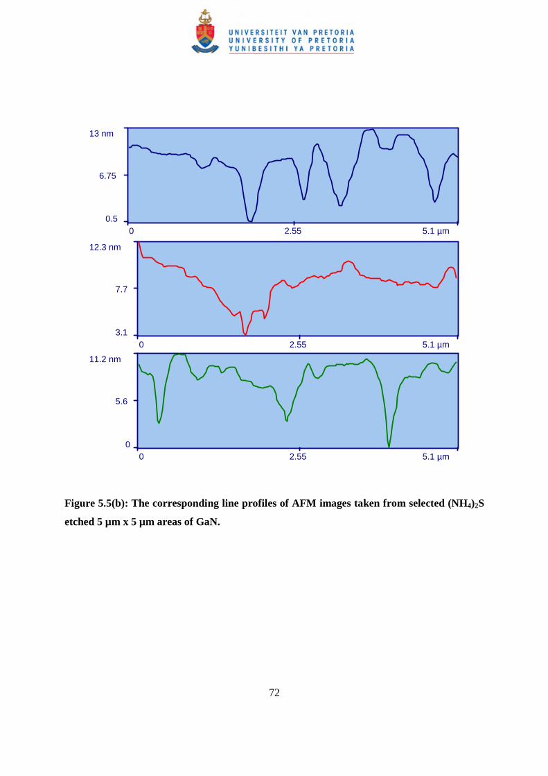
72
Figure 5.5(b): The corresponding line profiles of AFM images taken from selected (NH4)2S
etched 5 µm x 5 µm areas of GaN.
0.5
6.75
13 nm
0 2.55 5.1 µm
3.1
7.7
12.3 nm
0 2.55 5.1 µm
0
5.6
11.2 nm
0 2.55 5.1 µm

73
The as grown surface has needle-shaped protrusion as shown in Figure 5.1(a) and (b) is the
corresponding line profile. Using Rt, we compared the difference in features, ranging from
protrusions to craters. From Rt measurements, the average height of the protrusions on the
surface of the degreased samples was found to be 20.05 nm, as shown in Table 5.2. The second
surface, represented in Figure 5.2(a) and (b), was cleaned in aqua regia and shows a
disappearance of the protrusions and the emergence of craters, which are hexagonal in shape,
with Rt value decreasing to 2.5 nm. This observation implies that the chemicals used thus far,
were able to act on the protrusions on the as degreased surface, characterizing GaN by showing
hexagonal structure of the crystal.
Table 5.2: Statistical Characterization of GaN samples by AFM.
Cleaning
Procedure
Maximum topography
variation (R t-nm)
Mean topography
variation (Rp-nm)
RMS surface
roughness
Roughness factor
degrease 20.05 11.27 1.74 1.006
aquaregia 2.5 1.55 0.4 1.060
HCl 13.36 7 2.02 1.010
KOH 11.03 4.03 2.1 1.077
(NH4)2S 8.74 2.74 1.2 1.098
The next step is etching the surface in HCl, and it is observed that protrusions are disappearing
from the surface and craters are increasing, as shown in Figure 5.3(a) and (b). These craters are
either isolated or joint to form a bigger crater on the surface and the value of Rt increasing to
13.36 nm, indicating deeper craters as protrusions are removed. The surface protrusions seem to
have changed shape, from needles to rounded protrusions. The use of KOH on the surface, as
shown in Figure 5.4(a) and (b), shows that the protrusions appeared to be white and flat shaped.
In Figure 5.5(a) and (b) the surface of the samples cleaned in (NH4)2S are shown. The
protrusions on this surface are quite similar to the ones on the KOH etched surface. A two
74
dimensional (2D) image of the sample cleaned in (NH4)2S is shown in Figure 5.5 (a), confirming
that the observed protrusions on the surface are part of the crystal.
The density of craters on each of the three last cleaning processes is similar, particularly for the
HCl and KOH surfaces at approximately 6.2 x 108cm-2. The (NH4)2S surface has a little lower
density of craters at approximately 5.3 x 108 cm-2. The approximated density of craters is similar
to the dislocation density of the GaN used in this experiment, which is approximated to be 107 to
108 cm-2. Comparing the cleaning procedures, it was found that GaN was etched along the
threading dislocation. Threading dislocations have been found to be dominant defects in GaN
from TEM studies. In addition, the observed decrease in the density of the craters shows that a
new surface has appeared. It has been observed from TEM studies that threading dislocation
decrease gradually away from the interface [9]. KOH has been used to characterize defects in
GaN, and the defects density was found to be 2 x 109 cm-2. Different values of defect densities
have been recorded as 3 x 107 cm-2 and 4 x 107 cm-2 on N-face, and 1 x 107 cm-2 and 5 x 105 cm-2
on Ga-face. The understanding of the mechanisms for the formation thereof, will lead to the
reduction of these defects [10].
Using line profiles, statistical parameters were deduced from the AFM for each of the cleaning
procedures and are shown in Table 5.2 [11]. From the analysis of these data, the morphologies of
differently cleaned surfaces differ from one cleaning method to the other. The value of Rt
changed from 20.5 nm for degreased sample to 2.5 nm after aqua regia treated, implying a
removal of surface protrusions. The last three etch processes also differ in the value of Rt,
indicating how one chemical is able to etch the GaN surface. KOH and (NH4)2S each were able
to produce new surfaces as compared to HCl, which was not able at producing a new surface.
The other parameters, Rp, RMS roughness and the roughness factor all confirm the Rt values.
The highest RMS roughness is from the KOH etched surface and the lowest is from the aqua
regia cleaned surface. Furthermore, using RMS roughness parameter, we have compared the
stoichiometries on each of the cleaned surfaces, and stoichiometry and RMS roughness are
compared as shown in Figure 5.6.

75
Figure 5.6: Graph of root mean square (RMS) surface roughness and Ga/N ratio from AES
elemental surface concentrations.
5.3.2 Auger Electron Spectroscopy
AES was used to analyze the surface contaminants and the results are shown in Figure 5.7. The
effect of the cleaning procedure is seen in the reduction of O and C peaks. In addition to
reducing C and O peaks, HCl in aqua regia and (NH4)2S, respectively, added Cl and S to the
surface. The atomic percentage of surface elements present on every surface after wet chemical
cleaning procedures was calculated from the relative sensitivity factors. These contaminants may
be of advantage to the metal contact formation on the GaN surface as bonding with Au may be
enhanced and adhesion improved. Furthermore the use of sulfurants, alkenoids and halogens has
proved to enhance adhesion of metals such as Au, Ag, Pt, Pd and Ni to semiconductor surfaces
[12,13].

76
AES surface scans of cleaning preocedures
Electron Energy (eV)
200 400 600 800 1000
Aug
er P
eak
Inte
nsity
(A
rbitr
ary
Uni
ts) O
N
C
Cl
a) degrease
b) HCl etch
c)(NH4)2S
d) KOH
Ca
S
Ga
Figure 5.7: AES surface scans of GaN surface cleaned as indicated.
Comparing the AES surface scans of HCl and (NH4)2S, it is found that using HCl on the GaN
surface reduced the O peak, added Cl, and the use of (NH4)2S prevents re-oxidation of the
surface, adding insignificant amount of S, and reducing the Cl contaminant. This result further
confirms the importance of using (NH4)2S as a chemical that prevents re-oxidation of surfaces.
KOH removed all the Cl from the surface, and reduced the C significantly.
There had been reports of improved electrical characteristics of metals/GaN contacts after
treatments in HF, HCl, and NaOH. E. J. Miller et al has reported the reduction of reverse bias
leakage current in GaN Schottky diodes after treatment in NaOH. The high concentration of
OH-ion on the GaN surface is attributed to the reduction of reverse bias leakage in their
Schottky contacts [14]. In another report, Y-J Lin et al has reported the reduction of surface

77
states on InGaN using (NH4)2S [15]. Electrically, (NH4)2S was reported to reduce the Schottky
barrier height. In particular, it was reported that Ga-O, In-O and C-O bonds were removed from
the InGaN surface after (NH4)2S treatment. Furthermore, repeated exposure of the surface that
has a Cl peak to the electron beam in the AES system has resulted in desorption of the surface
contaminants, and consequently, complete removal of the Cl peak.
To further analyse the cleaned surfaces, the ratio of Ga/N, and RMS surface roughness are
plotted as a function of cleaning method, as shown in Figure 5 above. There is a relationship
between the RMS surface roughness and the contaminants on the surfaces, which consequently
affects the Ga/N ratio. The as grown surface shows a very high surface roughness and Ga/N ratio
and the cleanest surface shows lowest surface roughness and Ga/N ratio. Therefore as the surface
is cleaned, the surface roughness reduces as the Ga/N ratio improves, implying that the
chemicals used has etch GaN surface to removes contaminants. The RMS surface roughness of
KOH etched surface, differ from the as grown surface by about 0.4 nm. Different wet chemicals
used previously in removing contaminants on GaN have shown no effect on the surface
roughness of the material [2,3]. The work done previously to etch and remove surface GaN to
form etch steps were not achieved by using HCl and KOH [15]. Ultraviolet light illumination and
addition of ions were used to etch GaN successfully in KOH [16].
Previous results have recommended the use of thermal desorption after every chemical clean, to
completely remove surface contaminants [1,2,3]. In this work, we have found that thermal
cleaning of the degreased GaN surface resulted in almost complete removal of surface
contaminants. Figure 5.8 is a typical temperature profile of a sample cleaned in UHV under high
temperatures. This profile may be divided into two regions: region 1 from 23°C to 500°C and
region II from 500°C to 1010°C. In region I the carbon peak first decreases and then increases as
temperature increases. In region II, the carbon coverage on the surface of GaN decreases until it
drops to below AES detection limit, where average peak-to-peak height is less than 1.5. In the
case of oxygen, the surface coverage starts increasing and quickly decreases sharply until the
temperature of about 500ºC. At this temperature, all oxides are removed from the surface
according to AES sensitivity, in which average peak-to-peak height is less than 0.5. The increase
in O from 23°C to 50°C may be attributed to the removal of common surface water that had been

78
covering the surface prior to thermal heating. This water is very sticky and is usually removed at
temperatures above 220 °C. On the other hand, the increase in C may be due to segregation from
the bulk, which needs further study to confirm.
Figure 5.8: Surface concentration profiles of O and C on GaN surface during thermal
anneal in the AES.

79
5.4 Conclusions In conclusion, the effectiveness of wet chemical cleaning of GaN with different solutions, have
been characterized by AFM and AES. AFM results have shown that GaN surface roughness is
affected by the cleaning method used on the surface. Surface defects were characterized by
different etch chemicals, with (NH4)2S producing a defects free interface. AES has shown the
contaminant as C and O and that using HCl and (NH4)2S, will leave Cl and S on the surface. This
result has given sufficient information on removal of surface contamination; stoichiometry;
surface roughness and chemical etch. Using (NH4)2S prevented re-oxidation of the surface, and
further removes Cl from the surface of the GaN. KOH effectively removes the C on the surface.
The effects of S and Cl on the surface may enhance adhesion of metals to GaN surface, thus
improving device quality. Further work is necessary in finding the effects of different cleaning
procedures on the optical properties of the material and electrical properties of devices.

80
REFERENCES
[1] Smith L. L, King S. W, Nemanich R. J, Davis R. F, Journal Electronic Materials 25
(1996) 805.
[2] King S. W., Barnak J. P., Bremster M. D., Tracey K. M., Ronning C., Davis R. F.,
Nemanich R. J., Journal of Applied Physics 84 (1998) 5248.
[3] Lee K. N., Donovan S. M., Gila B., Overberg M., Mackenzie J. D., Abernathy C. R.,
Wilson R. G., J. Electrochemical Society 147 (2000) 3087.
[4] Pelto C. M., Chang Y. A., Chen Y., Williams R. S., Solid State Electronics 45 (2001)
1597.
[5] Machuca F., Liu Z., Sun Y., Pianetta P., Spicer W. E., Pease R. F., Journal of Vacuum
Science and Technology A 20 (2002) 1784.
[6] Shul R. J., Vawter G. A.., Willison C. G., Lee J. W., Pearton S. J., Abernathy C. R., Solid
State Electronics 42 (1998) 2259.
[7] Nel J. M., Demanet C. M., Hillie K. T., Auret F. D., Gaiger H. L., Applied Surface
Science 134 (1998) 22.
[8] Deenapanray P. N. K., Auret F. D., Myburg G., Hillie K. T., Demanet C. M., Surface and
Interface Analysis, 26 (1998) 748.
[9] Jasinki J., Swider W., Liliental-Werber Z., Visconti P., Jones K. M., Reshchikov M. A.,
Yun F., Morkoc H., Park S. S., Lee K. Y., Applied Physics Letters 78 (2001) 2297.
[10] Morkoc H., Materials Science and Engineering R33 (2001) 135.
[11] Zymierska D., Auleytner J., Kobiela T., Dus R., Physica Status Solidi(a) 180 (2000) 479.
[12] Wang J., Zeng B., Fang C., Zhou X., Journal of Electroanalytical Chemistry 484 ( 2000)
88.
[13] Shalish I., Shapira Y., Burstein L. and Salzan J., Journal of Applied Physics 89 (2001)
390.

81
CHAPTER 6
Experimental Results
Study of metal contacts on GaN for transmission of UV light
6.1 Introduction
Schottky barrier metal-semiconductor contacts are a choice device for the fabrication of
ultraviolet [1]. They have simple fabrication technology; suffer lower breakdown voltages, have
larger leakage currents at lower voltages as compared with p-n structures of the same
semiconductor material. Thus the formation of Schottky contact with high barrier height, low
leakage current [2], and good thermal stability [3] to withstand high temperature processing and
operation are some of the most important factors in improving the performance of Schottky
barrier photodiodes to be used for ultraviolet detection.
Different metals have been used for the formation of such contacts, including Au, Ni and Ni/Au.
Sheu et. al. have discovered the high transparency of Ni/Au contacts to GaN, using the metal
structure for ohmic contacts to p-GaN. After annealing the contacts at 550 °C, they recorded a
transmittance of above 80 %, after forming NiO [4]. NiO is a transparent wide bandgap
semiconductor which is very easy to fabricate by annealing Ni in air or in oxygen. This
semiconductor is p-type with a bandgap of 4.3 eV [5]. NiO has been used to study the electrical
properties of oxidized Au/NiOx/p-GaN ohmic contact and found that annealing this structure is
the main mechanisms that is responsible for the ohmic contact nature of the system [6].
Furthermore, NiO/ZnO structure has been used to study the defects in ZnO [7]. The optical
transmittance of 5 nm Au and Ni ultra-thin films is less than 40 % [8]. In this work, we report on
the study of Au, Ni, and Ni/Au contacts onto GaN for the fabrication of ultraviolet detectors.

82
6.2 Choice of metal for transparent contacts
In fabricating UV detectors of Schottky type to GaN, the metal contact must be transparent to
UV light. Published works have used a metal layer of high work function and 10 nm thickness
onto GaN [2]. A computer modeling program was used, employing the knowledge of the
absorption coefficient of GaN and the metal thickness. UV light was focused onto metal/GaN
structure and the transmission percent of the structure as a function of UV wavelength range
from 240 to 400 nm was recorded. The choice of the metals was due to high work function and
availability. Metals with high work function produce high barrier height for Schottky diodes onto
semiconductors. Figure 6.1 show the simulation results of the designed metal/GaN photodiodes
using different metals. The result of the model made Ag, Au, Ni suitable candidates for
fabrication of UV detectors. Ag was abandoned as it was oxidizing easily.
Figure 6.1: Simulation results for the designed metal/GaN photodetector, with Au being
highly transparent.

83
6.3 Experimental
GaN samples were degreased in trichloroethylene and isopropanol; then boiled in aquaregia and
finally etched in HCl: H20 (1:1). Ti/Al/Ni/Au (15 nm /220 nm /40 nm /50 nm) ohmic contacts
were electron-beam deposited onto samples and annealed at 500 °C for 5 minutes in air. Circular
Au, Ni and Ni/Au Schottky contacts of diameter 0.6 mm were resistively evaporated onto GaN
through a metal mask at room temperature. To ensure temperature stability during deposition, the
glass dome was cleaned of all metal residues before loading the samples for metallization. The
thickness of the Au and Ni layers was 10 nm, and that of Ni/Au was 5/5 nm. Atomic Force
Microscope (AFM) was used to study the morphology of Ni and Au onto GaN. Auger Electron
Spectroscopy (AES) was used to characterize the Ni/Au layer after annealing in air for 5 minutes
at 550 °C. Current voltage (I-V) measurements were taken using an HP4140B pA meter/DC
source for all metal contacts.
6.4 Results and Discussion
Analysis of the metal films for continuity using AFM is presented in figure 6.2. The surface
structure of all particles, even inside the etch pits, was found to be the same, indicating that the
10 nm metal film is continuous. Comparing Au and Ni, it is found that their surface structures on
GaN differ. Ni films present smooth morphology and Au shows grained structures. The RMS
roughness of the 10 nm Au and Ni are 25.6 and 22.7 nm respectively. Choosing an area without
any etch pits, it was found that the peak-to-valley surface roughness of Ni films was
approximately 9,0 Å and RMS roughness of 1.5 Å shows that the Ni films are relatively smooth.
The Au peak to valley roughness was recorded as 11 nm and the RMS roughness 2.3 nm.
84
a) 10 nm Au layer
b) 10 nm Ni layer
Figure 6.2: The AFM images of 10 nm Au and Ni.

85
Figure 6.3 shows the Auger peak to peak heights (APPH) depth profiles as a function of
sputtering time for as deposited (a) and annealed (b) at 500°C Au/Ni/GaN in air. The elements
presented on the surface before anneal are Au, Ni, Ga, N and O as indicated. Figure 6.3(b) shows
the formation of sandwiched layers after anneal. At highest APPH, we identify Au layer,
presenting a compound as a result of annealing. The compound may be due to diffusion of
elements during annealing. O and Ni compounds are also identified, followed by Ga and N
compound. A diffused layer of Ni and Ga is seen at the beginning, showing a possible diffusion
of Ni into GaN. At the end of sputtering, the depth profiles show that there exists a 1:1 ratio of
Ni and O, indicating possible formation of NiO.
86
0 2 4 6 8 10 12 14
AP
PH
(ab
itra
ry u
nit
s)
0
2
4
6
8(a) as deposited
(b) annealed
Time (minutes)
0 5 10 15 20 25
AP
PH
(arb
itra
ry u
nit
s)
0
1
2
3
4
5
Au
Ga
N
Ni
O
(b) annealed
I
II
III
Figure 6.3: AES profiles of sputtered GaN/Ni/Au surface, (a) as deposited and (b) annealed.

87
Figure 6.4 is the RBS peak of Au, showing that Au has diffused into the Au/Ni/GaN structure
during annealing so that we have a stack of compounds on GaN in agreement with AES results.
In figure 6.3 (b), region I indicate the compound of Au, possibly with Ni as Au diffuses into the
sample. A study of correlation of contact resistance with metal diffusion was done by Hu et. al.
[9], using RBS. It was found that annealing Au/Ni/p-GaN for 10 minutes in air, Au diffused into
the sample towards Ni and an out diffusion of Ni to the surface, resulting in the formation of
NiO. Region II shows GaN compound and region III shows the formation of NiO.
GaN-Ni-Au
Ta = 500
oC, t
a = 5 min
Channel Number
360 380 400 420 440
Co
un
ts
0
2000
4000
6000
8000
10000
12000
14000
Figure 6.4: RBS spectra of Au profile, showing the as grown and annealed at 500 °C, where
Au is seen to diffuse towards the interface.

88
A further study was done with 100 nm Ni onto GaN, annealed in air for one hour, to understand
the compound formed at the Ni/GaN interface. In this study, XRD and SEM were used to
analyse the samples. Figure 6.5 gives the XRD results indicating the formation of NiO and
residual Ni onto GaN after 1 hour anneal. Electron Diffraction Spectroscopy (EDS) analysis of
the annealed sample confirmed the observation, with ratio of Ni and O as almost 1:1. This is in
agreement with work done by Nel et. Al., where it was shown that NiO formed at 500°C with no
evidence of Ni2O3 phase [10].
2 Theta (Cu k-alpha)
42 43 44 45 46 47
Co
un
ts
0
5000
10000
15000
20000
25000
NiO(200)
Ni(111)
Figure 6.5: XRD patterns of oxidised Ni at 500°C showing the formation of NiO.

89
Figure 6.6 shows the current voltage mechanism of Au, Ni and Ni/Au contacts onto GaN. The
Schottky barrier height of Au contacts was obtained as 0.81 ± 0.02 eV. Series resistance for these
contacts was about 481 ± 4 Ω. The current-transport mechanisms are dominated by thermionic
emission at lower voltages and series resistance effect depicted clearly at higher voltages.
Generally Au contacts age very quick due to the problem of adhesion to GaN. The Schottky
barrier height of Ni contacts was obtained as 0.78 ± 0.04 eV Series resistance for these contacts
was about 38 ± 1 Ω, far less than that of Au contacts. Ni/Au contacts are annealed at 500 °C for
transparency. The leakage current of Ni/Au is two orders of magnitude lower than that of Ni, and
the Schottky barrier height was averaged at 0.92 ± 0.01 eV. Current transport mechanisms are
clearly displayed with generation-recombination dominating the lower voltage region. In the
high voltage region, the diode characteristics are affected by series resistance. The presence of
NiO onto GaN reduced the leakage current by two orders of magnitude.
Bias (V)-1.5 -1.0 -0.5 0.0 0.5 1.0 1.5
C
urr
en
t(A
)
10-11
10-10
10-9
10-8
10-7
10-6
10-5
10-4
10-3
10-2
Au
Ni
Ni/Au
Figure 6.6: Curent-Voltage plots of Au, Ni and Ni/Au contact on n-GaN. Ni/Au was
annealed at 500 °C while Ni and Au are 10 nm each thick are not annealed.

90
6.5 Conclusions
In conclusion, Au, Ni and Ni/Au contacts onto GaN were fabricated and characterized. AFM
showed that 10 nm thick Au and Ni contacts onto GaN were continuous with peak-to-valley
surface roughness of Ni films approximately 9.0 Å and RMS roughness of 1.5 Å while Au peak
to valley roughness was recorded as 11 nm and the RMS roughness 2.3 nm. Annealing Ni/Au
onto GaN produced a highly transparent and conductive NiO, as confirmed by XRD, SEM, AES
sputtering profiles and EDS analysis. I-V characteristics showed that Ni/Au contacts had the
lowest reverse leakage current, two orders of magnitude below that of Au contacts. The barrier
heights of the diodes were 0.81, 0.78 and 0,92 for Au, Ni and Ni/Au respectively.

91
REFERENCES
[1] Monroy E., Calle F., Munoz E., Omnes F., Gibart P. and Munoz J. A., Applied Physics
Letters 73 (1998) 2146.
[2] Osinsky A., Gangopadhyay V, Lim B. W., Anwar A. Z., Asif-Khan M., Kuksenkov
D. V. and Temkin H., Applied Physics Letters 72 (1998) 742.
[3] Luther B. P, Wolter S. D. and Mahoney S. E., Sensors and Actuators B, 56 (1999) 164.
[4] Sheu L. K., Su Y. K., Chi G. C., Koh P. L., Jou M. J., Chang C. M., Liu C. C. and. Hung
W. C., Applied Physics Letters 74 (1999) 2340.
[5] .Sawatzky G. A and Allen J. W., Physisical Review Letters 53 (1984) 2339.
[6] Liday J., Hotovy I., Sitter H., Vogrincic P., Vincze A, Vavra I, Satka A., Ecke G.,
Bonnani A., Breza J., Simbrunner C. and Plchberger B., Journal Materials Science 19
(2008) 855.
[7] Auret F. D., Wu L., Meyer W. E., Nel J. M., Legodi M. J. and Hayes M., Physica Status
Solidi (c) 1 (2004) 674.
[8] Su Y. K, Chang S. J, Chen C. H, Chen J. F., Chi G. C, Sheu J. K., Lai W. C. and Tsai J.
M., IEE Sensors Journal 2 (2002) 7361
[9 ] Hu C. Y., Ding Z. B., Qin Z. X., Chen Z. Z., Yang Z. J., Yu T. J., Hu X. D., Yao S. D.
and Zhang G. Y., Semiconductor Science and Technology 21 (2006) 1261.
[10] Nel J. M., Auret F. D., Wu L., Legodi M. J. and Hayes M., Sensors and Actuators B:
Chemical 100 (2004) 270.

92
CHAPTER 7
Chemical treatment effect on Au/GaN diodes
7.1 Introduction
Rectifying contacts with low leakage currents and high barrier height are required for the
successful fabrication of GaN-based devices. Schottky barrier diodes (SBD) are the choice
structure for many semiconductor devices, including microwave diodes, field-effect transistors
and photodiodes [1,2,3]. Their technological importance requires a full understanding of the
nature of the electrical characteristics of SBDs. It is well known that SBD has a thin layer of an
oxide between the metal and the semiconductor, which cannot be removed by conventional
chemical cleaning. Such an oxide converts the diode to metal-insulator-semiconductor (MIS) and
usually influences the electrical characteristics of the diode, causing a change in the interfacial
charge with bias, giving rise to an electric field at the interfacial layer between the metal and the
semiconductor [4,5]. The oxide layer reduces the barrier height and consequently increases the
series resistance.
Generally, the forward biased current-voltage (I-V) characteristics are linear in the semi-
logarithmic scale at low voltages, but deviate considerably from linearity due to the effects of
series resistance, sR resulting from the presence of the thin oxide layer and other surface
contaminants. The series resistance is only effective in the curvature downward region or non-
linear region of the forward I-V characteristics at sufficiently high voltages. The concavity of the
current-voltage characteristics at higher voltages increases with increasing series resistance.
Increasing series resistance decreases the barrier height and this result in non-ideal current-
voltage characteristics. Other parameters such as the ideality factor, n(V) and zero biases-barrier
height, ,0b are effective in both the linear and the non-linear regions of the I-V curve,
accompanying the changes in the Schottky barrier height (SBH) [6]. The effect of the series
resistance between the depletion region and the ohmic contact of the neutral region of the
93
semiconductor bulk causes the I-V characteristics of the metal-semiconductor contact to deviate
from the expected [7].
The interface states at the metal-semiconductor junction play a vital role in evaluating the
Schottky barrier height and the ideality factor. These manifest themselves as deviations from the
ideal Schottky barrier formation and are localized within a few atomic layers of the intimate
metal-semiconductor contact with energies which fall inside the forbidden gap. Bardeen showed
that such charge accumulated at the metal-semiconductor contact reduces the effective potential
difference between the semiconductor and the metal contact [8]. Interface states arises from
semiconductor surface states due to discontinuity in the lattice potential, metal-induced-gap sates
due to wave-function tunneling from the metal into the semiconductor, surface states due to
contamination and defects; and any new compounds formed as a result of the interaction of the
metal and the semiconductor.
A study of the importance of series resistance in calculating the characteristics parameters of Si
Schottky contacts was done by Aydin et al [7], obtaining their estimations from determination of
interface states density distribution from the analysis of the current voltage measurements.
Kampen and Monch studied the barrier heights of different metals on GaN using metal-induced
gap states (MIGS) and the electronegativity model, concluding that the experimental values of
the barrier height are excellently reproduced by the theoretical predictions, which follow from
physical MIGS and the electronegativity concept [9]. A review of metal-contact technology has
revealed the importance of surface preparation prior to metal deposition [10].In this study, two
different surface chemicals were used to treat GaN surface prior to metal deposition. The effects
of chemical treatments on Schottky characteristics were investigated using capacitance-voltage
(C-V) and current-voltage (I-V) characteristics. The average barrier height for the diodes was
1.43 and 1.20 eV for C-V; and 0.81 and 0.89 for I-V measurements respectively.

94
7.2 Experimental.
For this investigation, we have used GaN samples with carrier density of 1 x 10¹⁷
cm-3
, obtained
from TDI. Before contact fabrication, samples were cleaned using trichloroethylyne (TEC),
Isopropanol and HCl:HNO3 aquaregia. Each of the samples was finally etched in 1:1 HCl:H2O
(sample 1) and (NH4)2S (sample 2) respectively. Using patterned surface, Ti/Al/Ni/Au
(150/2200/400/500 Å) ohmic contacts were deposited by electron-beam and annealed in ultra
pure Ar for 5 minutes at 500 °C. Thereafter, Au Schottky contacts, 0.25 mm thick, were
deposited in the resistive evaporator at room temperature. The values of zero-biased barrier
height and ideality factor were determined from I-V and C-V measurements at room temperature
and corrected afterwards for the effect of series resistance.
7.3 Results and Discussion
7.3.1 Capacitance-Voltage
In Schottky diodes, the depletion layer capacitance can be expressed as [1 ]
2
2
2( )bi A
s D
V VC
q A N (1)
where A is the area of the diode, biV the diffusion potential at zero bias and is determined from
the extrapolation of the linear 2C V plot to the V axis, and
AV is the applied voltage. The value
of the barrier height can be obtained from the relation:
,0 0( )b biC V V V (2)
where 0V is the potential difference between the bottom of the conduction band and the Fermi
level; and can be calculated knowing the donor concentration DN obtained from the following
relation:
(3)
where 16 34.6 10CN cm is the effective density of states in the conduction band [2].

95
Nine dots with the same diameter (0.25 mm) on each sample were evaluated. Figure 7.1 shows
the reverse bias 2C V characteristics for one diode from sample 1 and sample 2 respectively.
For these particular diodes on samples 1 and 2, the C-V barrier heights are 1.43 and 1.20 eV
respectively. The carrier concentration of 1.9 x 10¹⁶
and 2.4 x 10¹⁶
cm-3
from the reverse bias
2C V plots were obtained for sample 1 and sample 2. The C-V barrier heights ranged from
1.28 to 1.50 eV for sample 1 and from 1.14 to 1.25 eV for sample 2. The statistical analysis for
the C-V data yielded SBH mean value of 1.35 ± 0.04 eV for t sample 1 dots and SBH mean
value of 1.20 ± 0.03 eV for sample 2.
Bias (V)
-1.0 -0.8 -0.6 -0.4 -0.2 0.0
1/C
2 (
F-2
x 1
02
0)
0
1
2
3
4
5
Sample 2
Sample 1
Figure 7.1: Reverse Bias C2-V curves of the HCl and (NH4)2S samples. For these particular
diodes on samples 1 and 2, the C-V barrier heights are 1.43 and 1.20 eV respectively.
7.3.2 Current-Voltage

96
In Schottky barrier diodes, the barrier height depends on the voltage and surface conditions prior
to metal deposition. The surface condition includes the thickness of the interfacial oxide, which
affects the current-transport mechanisms. These include the thermionic emission, which is
characterized by ideality close to unity and thermionic field emission and field emission. These
mechanisms are affected by series resistance, tunneling and generation recombination in the
depletion region. Table 1 gives the summary of the electrical characteristics of the diodes.
Table 7.1: Values obtained experimentally from the current-voltage characteristics of the
Au/GaN Schottky diodes. The difference in series resistance for the sample 1 and 2 is due to
the surface state after different chemical treatment.
For a Schottky contact with series resistance, the net current of the device is due to thermionic
emission and it is written as [1]:
0
( )exp A sq V IR
I InkT
(4)
where the saturation current0I is expressed as
,0* 2
0 expbq
I AA TkT
(5)
where q is the electron charge, *A is the effective Richardson constant and is equal to
26A/cm2K
2 for n-type GaN [11], A is the diode area, T is the absolute temperature, k Boltzmann
97
constant, n the ideality factor of the SBD and .0b
the zero bias barrier height. When VA ≥
3kT q , the extrapolated current, 0I ,and the zero bias barrier height can be expressed as
2
,0
0
lnb
kT A AT
q I (6)
and the ideality factor from equation 4 can be written as
ln
q dVn
kT d I (7)
The ideality factor of the SBD, n is a measure of the conformity of the diode to pure thermionic
emission. From figure 7.2, current-transport mechanisms displayed are thermionic emission and
the series resistance effect at high voltages. The values of the ideality factor, n, and the barrier
height bwere calculated from the forward I-V characteristics according to (6) and (7). For
sample 1 the barrier height, .0b
ranged from 0.79 to 0.89 eV and the ideality factor n ranged
from 1.02 to 1.17. Sample 2 .0b
values ranged from 0.71 to 0.85 eV and the n from 1.31 to
1.36. The statistical analysis yielded mean values of 0.84 ± 0.05 eV for the 1.06 ± 0.50 for
barrier height and ideality factor of sample 1 (9 dots) respectively and the mean values of 0.80 ±
0.01 eV and 1.34 ± 0.20 (9 dots) for sample 2 diodes. Ideality factors above unity has been
attributed to: interface states due to thin oxide layer between the metal and the semiconductor,
including other contaminants, tunneling currents in highly doped semiconductors, image-force
lowering of the Schottky barrier in electric field at the interface, and generation-recombination
currents within the depletion region [1]. Our previous results have shown S and Cl residues onto
GaN after cleaning in HCl and (NH4)2S using Auger Electron Spectroscopy (AES) and X-ray
Photoemission Spectroscopy (XPS) [12]. The work done on GaAs and GaP nitrididation has
shown anion exchange where a thin layer of Ga-N was formed on each of the materials [13].
Surface Ga-N in turn passivates the GaAs and GaP, affecting the I-V and C-V characteristics of
these materials. In addition, the work done by Liu et al has shown that the Ga peak becomes
larger when samples are cleaned in (NH4)2S than in HF/HCl [14]. Furthermore, (NH4)2S has
been found to reduce the barrier height on GaN, and preventing re-oxidation of the surface [15].
We suggest that there exist Ga-Cl and Ga-S on sample 1 and sample 2, respectively. Previous

98
XPS results have shown that as-grown GaN surface has oxides in the form of Ga2O3 and GaOH
[12]. In addition, while rinsing GaN in water, addition of OH to GaN to form the GaOH, may
occur, and be part of sticking surface water that may contribute to interface states [16].
Bias (V)
-3 -2 -1 0 1 2 3
Cu
rren
t (A
)
10-13
10-12
10-11
10-10
10-9
10-8
10-7
10-6
10-5
10-4
10-3
10-2
10-1
Sample 2
Sample 1
Figure 7.2: I-V curves of the treated samples. The series resistance values of HCl samples
are generally higher than those treated in (NH4)2S, which presented less oxide and reduced
barrier height
The values of sR and
.0b for both sample 1 and 2 were obtained as 0.82 eV and 22.3 Ω; and
0.71 eV and 17.0 Ω respectively. As mentioned above, the barrier height values of 1.43 and 1.20
eV for sample 1 and 2 were obtained from the C-2
-V plots, respectively. These barrier height
values obtained from the C-2
-V (1.43 eV) and I-V characteristics (0.89 eV) are different from
each other by 0.54 eV. We attribute the difference between the I-V and C-V barrier height in the
metal-semiconductor to SBH inhomogeneity. This is the fact that the barrier heights of the

99
diodes on the same sample differs from diode to diode and at different positions on the same
diode. The measured I-V barrier height is significantly lower than the weighted arithmetic
average of the SBHs. On the other hand, the C-V measured barrier height is influenced by the
distribution of charge at the depletion region follows the weighted arithmetic average of the
barrier height inhomogeneity; hence the BH determined by C-V is close to the weighted
arithmetic average of the barrier heights. Therefore, the barrier height determined from zero bias
intercept assuming thermionic emission as current transport mechanism is well below the
measured BH and the weighted arithmetic average of the barrier heights [17,18]. Furthermore,
the surface damage at the metal-semiconductor-interface affects the I-V measurements because
defects may act as recombination centers for trap-assisted tunneling currents. C-V
measurements are generally less prone to interface states, so that the determined barrier height is
considered more reliable, though the depletion width can be altered by the interface defects if
they are deeper into the space charge region [19].
7.4 Conclusions
In conclusion, we have fabricated Au/n-GaN SBDs using different cleaning procedures. From
the current-voltage characteristics, we obtained the values of ideality factor, SBH, and sR for the
samples. I-V characteristics are near ideal with thermionic emission as the dominant current
transport mechanism. Furthermore, HCl treated samples behave like a MIS diode due to the
amount of oxide remaining on the surface after treatment. The series resistance values of HCl
samples are generally higher than those treated in (NH4)2S, which presented less oxide and
reduced barrier height, in agreement with published results. Most published results on GaN have
only reported their findings without specifics on current transport mechanism. Thus further work
is needed for the investigation ideality factor far above unity, which will need the knowledge of
the oxide layer thickness on GaN, effects of passivation of GaN surface on electrical
characteristics, and analysis of barrier height inhomogeneities on the rectifying diode
characteristics on GaN.

100
REFERENCES
[1] Rhoderick E. H. and Williams R. H., Metal-Semiconductor Contacts, Oxford, Clarendon,
(1988).
[2] Sze S. M., Physics of Semiconductor Devices, 2nd
Edition, New York, Wiley (1981).
[3] Wang L., Nathan M. I., Lim T-H, Asif Khan M. and Chen Q, Applied Physics Letters 68
(1996) 1267.
[4] Hanselaer P., Laflere W.H., Meirhaeghe R. L. and Cardon F., Applied Physics Letters 56
(1984) 2309.
[5] Monroy E., Calle F., Pau J.L., Muńoz E. and Omnes F., Electronic Letters 36 (2000)
2096.
[6] Card J. C. and Rhoderick E. H., Journal of Applied Physics: D 4 (1971) 1589.
[7] Aydin M. E., Akkiliç K. and Kiliçoğlu T., Applied Surface Science 225 (2004)1304.
[8] Bardeen J., Physical Review, 71 (1947) 771.
[9] Kampen T. U. and Monch W., Applied Surface Science 117/118 (1997) 388.
[10] Liu Q. Z. and Lau S . S., Solid State Electronic 42 (1998) 677.
[11] Schmidt A. C., Ping A. T., Asif Khan M., Chen Q., Yang J. W. and Adesida I.,
Semiconductor Science and Technology, 11 (1996) 1464.
[12] Diale M., Auret F. D., Van der Berg N. G., Odendaal R. Q. and Roos W. D., Applied
Surface Science 246 (2005) 279.
[13] Bruno G., Applied Surface Science 235 (2004) 239.
[14] Liu J., Shen B., Zhou Y. G., Zhou H. M., Wang M. J.,. Zheng Z. W, Zhang B., Shi Y. and
Zheng Y. D., Optical Materials 23 (2003) 133
[15] Cao X. A., Pearton S. J., Dang G., Zhang A. P., Ren F. and Van Hove J. M., Applied
Physics Letters,75 (1999) 4130.
[16] Diale M., Auret F. D., Van der Berg N. G., Odendaal R. Q. and Roos W. D., Surface and
Interface Analysis 37 (2005) 1158.
[17] Werner J. H. and. Guttler H. H, Journal of Applied Physics, 69 (3) (1991) 1552.
[18] Tung R. T., Levi A. F. J., Sullivan J. P. and Schrey F., Physical Review Letters 66
(1971) 72.
[19] Fontaine C., Okumura T. and Tu K. N., Journal of Applied Physics 54 (1983) 1404.

101
CHAPTER 8
Fabrication and characterization of GaN and
AlGaN Schottky barrier photodiodes
8.1 Introduction
GaN is a wide bandgap semiconductor that has been explored for the fabrication of ultraviolet
photodiodes suitable for operations in chemically harsh and high temperature environments [1].
Alloying of Al with GaN to form AlGaN has a very important property called solar-blindness,
which makes the material insensitive to visible light [2]. Intrinsic solar-blindness is a bandgap
dependent property of the semiconductors [3]. The bandgap of GaN and AlN are 3.4 and 6.2 eV
respectively, which makes AlGaN bandgap to lie between the two extremes for the specified Al
content. [4]. Similar to GaN, the growth of AlGaN had issues such as lack of suitable substrate,
resulting in cracks in the thin film [5]. AlGaN grown on sapphire has high densities of threading
dislocation which increases with increasing Al content [6]. Threading dislocations are
detrimental to devices as they are a major reason for high leakage currents and reduced spectral
responsivity in semiconductor photodiodes [7]. There has been much progress in the growth of
AlGaN, with the use of AlN nucleation layer to reduce cracks in the AlGaN film [8].
Schottky barrier photodiodes are used in applications such as missile warning and guidance,
flame monitoring and prevention of skin cancer [9]. Thus far, various types of GaN-based
photodetectors have been reported, with low dark current, high response speed, and high
detectivity [10]. They have reported low capacitance, which is an important component of large
bandwidth and low noise performance in photodetectors. Another important parameter is high
transparency of the metal used for Schottky barriers, which determines the number of photons
entering the semiconductor [11]. In this work, we have fabricated GaN and AlGaN Schottky
barrier photodiodes, using Ni/Au metallization system. The photodiodes were characterized in
our in-house electro-optical measurement station. The photodiodes gave zero biased dark
102
currents as small as 10-9
A (35.8 µA/cm2) for GaN and 2.8 x 10
-9 A (21.6 nA/cm
2) for AlGaN
(55% Al). The recorded reverse biased peak responsivity was 31.8 A/W with quantum efficiency
of 11 % when the wavelength of light is 369 nm in the case of GaN. AlGaN results have shown a
peak responsivity of 3.8 mA/W at 280 nm, with quantum efficiency of 1.7 %.
8.2 Experimental
GaN samples used in the experiment were 5.6 µm thick, grown by HVPE. AlGaN epitaxial
structures were grown by HVPE with 55 % Al content. This structure consist of 30 nm GaN
grown on sapphire followed by Si doped GaN film for the fabrication of ohmic contacts. The
following layer was 0.1 µm AlN, which is believed to reduce threading dislocations in AlGaN
film. The active layer was a thin film of 0.5 µm layer of Al0.55Ga0.45N. Samples were cleaned in
organic solvents, boiled in HCl:HNO3 aquaregia and a final etch in HCl, prior to loading in the
electron-beam deposition system for ohmic contacts consisting of Ti/Al/Ni/Au onto the top layer.
All rinsing was done in methanol. The ohmic contacts were then annealed in Ar ambient for 5
minutes at 500 °C.
The samples were then etched in HCl before loaded for the deposition of Schottky contacts in the
resistive evaporator, consisting of Ni/Au with thickness 5 nm each. Similarly, GaN photodiodes
were fabricated, using the same cleaning procedure and the same metals as with AlGaN for both
ohmic and Schottky contacts. For device characterization, current-voltage (I-V) measurements
were carried out. I-V measurements were taken using an HP4140B pA meter/DC source. Dark-
and photocurrent were measured from annealed samples. Wavelength dependent measurements
were done at the same I-V station with a deuterium lamp connected to the monochromator by
optical fibre. All measurements were performed at room temperature. Using the commercial SiC
and AlGaN photodiodes’ data sheets and the quantum efficiencies specified therein, the
irradiance was determined, which was then used to calculate the responsivities and quantum
efficiencies of the fabricated diodes.

103
8.3 Results and Discussion
The GaN photodiodes have recorded a zero biased dark current as low as 6.48 x 10⁻⁹
A
(35.8 µA/cm2) while that of AlGaN was 2.8 x 10
-9 A (21.6 µA/cm
2). Figure 8.1 (a) and (b)
shows the I-V characteristics of GaN and AlGaN photodiodes respectively. The barrier height of
0.67 eV was recorded for I-V measurements and the corresponding ideality factor of 2.48. The
series resistance of the diodes was 381 Ω. In the case AlGaN the I-V barrier height was 1.09. The
ideality factor for Schottky diodes fabricated on AlGaN was 1.35 with series resistance in
1090 Ω. Schottky diodes on GaN and AlGaN suffer from high series resistance. Series
resistance in AlGaN/GaN structures increases with increasing Al content and thickness of thin
film. High series resistance contributes to slow response and thermal noise of the photodiodes.
Schottky barrier GaN photodiodes with dark currents densities as low as 10-10
A/cm2 have been
reported [12]. The reported low current densities were measured at higher voltages of up to 50 V
when device active areas were differing from one device to the other. From the work done by
Jhou et al [13], in annealing the Ni/Au contacts in oxygen, low dark currents were observed. Our
Ni/Au contacts were annealed in air. Su et al [14], have compared GaN and AlGaN
photodetectors, where high quantum efficiencies and low noise levels in AlGaN were reported.
The fact that the ideality factors of the diodes are all far above unity, indicates that the total
current is a combination of current mechanisms, other than thermionic emission [15]. The low
values of barrier height show that we have fabricated GaN photodiodes which alows majority
carriers to easily cross from the metal to the semiconductor. Consequently, such diodes have
long cut-off wavelength, so that GaN-Ni/Au pair are correctly selected for UV detection. The
dark current can be further lowered by cooling the photodiodes.

104
Bias (V)
-1.5 -1.0 -0.5 0.0 0.5 1.0 1.5
Cu
rre
nt
(A)
10-9
10-8
10-7
10-6
10-5
10-4
dark
photo
Figure 8.1 (a): I-V characteristics of GaN photodiodes.

105
Bias (V)
-1.5 -1.0 -0.5 0.0 0.5 1.0 1.5
Cu
rre
nt
(A)
10-10
10-9
10-8
10-7
10-6
10-5
10-4
10-3
10-2
dark
photo
Figure 8.1 (b): I-V characteristics of AlGaN photodiodes.
Spectral responsivity measurements were done in the 150-450 nm range, using Deuterium lamp,
a single-pass monochromator and a calibrated SiC or AlGaN photodetector. The response curves
of commercial AlGaN and laboratory AlGaN are presented in figure 8.2, confirming the
optoelectronic station accuracy. The peak responsivity of the commercial AlGaN photodiode
occurred at 45.8 at 270 nm, with 21 % quantum efficiency. During the measurements, applied
voltage on the photodetector was varied from 0.1 – 0.5 V. The responsivity of a photodiode is a
measure of the effectiveness of the conversion of incident radiation into current or voltage and
can be expressed as [16]:
1
1.24
p
opt
I mqR AW
P h (1)
106
where , , , , ,p optI P q h and are the photocurrent, optical power, quantum efficiency, electron
charge, Plank’s constant, frequency and wavelength respectively. The irradiance of the lamp was
estimated from the factory settings of the detector; using the calibration values to evaluate the
optical power. Using equation (1) the peak responsivity, R of 31.8 mA/W was recorded for GaN
and 3.8 mA/W for AlGaN respectively. The maximum photo response occurred at 369 nm and
280 nm wavelengths for GaN and AlGaN photodiodes, as shown in Figure 8.3 (a) and (b)
respectively. Since λc< 280 nm was satisfied, true solar-blind detection was successfully
demonstrated for AlGaN photodiodes, while GaN satisfied the condition for visible-blind
photodiodes at λc< 380 nm [17]. The quantum efficiency (Q.E), defined as the percentage of
incident photons that contribute to the photocurrent, follows from equation (1) and is given by:
1240(100%) ( )
observed
ideal
R RhcR
R q nm (2)
Maximum quantum efficiency of GaN and AlGaN photodetector determined from the
responsivity value was about 11 % and 1.7% respectively. The low Q.E of AlGaN photodiodes
shows that very little light was absorbed.

107
Wavelength (nm)
200 220 240 260 280 300 320 340
Resp
on
siv
ity (
mA
/W)
-1
0
1
2
3
4
Resp
on
siv
ity (
mA
/W)
0
10
20
30
40
50
60
Commercial
laboratory
Figure 8.2: Photocurrent density response curves as a function of wavelength for AlGaN
UV detectors.

108
Wavelength (nm)
300 320 340 360 380 400
Re
sp
on
siv
ity
(A
/W)
0
5
10
15
20
25
30
35
340 360 380 400
Cu
rre
nt
den
sit
y (
A/m
m x
10
-4)
0.00
0.05
0.10
0.15
0.20
0.25
0.30
0.35
Figure 8.3 (a): Photocurrent density response curves as a function of wavelength for GaN
UV detectors

109
200 220 240 260 280 300 320 340
Cu
rre
nt
de
ns
ity (
A/m
m2 x
10-1
0)
-1.0
-0.5
0.0
0.5
1.0
1.5
2.0
2.5
200 220 240 260 280 300 320 340
Re
sp
on
siv
ity
-1
0
1
2
3
4
Wavelength (nm)
Figure 8.3 (b): AlGaN photocurrent density response curves as a function of wavelength.

110
8.4 Conclusions
In conclusion, we have demonstrated the fabrication of visible-blind GaN and solar-blind AlGaN
Schottky photodiodes with low zero biased dark currents. Device responsivity as high as
31.8 mA/W for GaN and 3.8 mA/W for AlGaN were recorded. The calculated quantum
efficiencies of the photodiodes were 11 % for GaN and 1.7 % for AlGaN respectively. The
barrier heights of 0.67 eV and 1.09 were recorded, for GaN and AlGaN photodiodes. The series
resistance of GaN was 178 Ω and that of AlGaN 1090 Ω. Ideality factors of 2.48 and 1.35 were
recorded for GaN and AlGaN respectively. The commercial and fabricated AlGaN photodiodes
have photocurrent density and responsivity maximum peaks occurring in the range of
270 - 280 nm. Further work will be done to improve the performance of AlGaN photodiodes.
For the structure studied here, there is a need to etch away the AlGaN and AlN layers so that
ohmic contacts are deposited onto GaN.

111
REFERENCE
[1] Razeghi M. and Rogalski A., Journal of Applied Physics, 79 (1996) 7433.
[2] Schreiber P., Dang T., Smith G., Pickenpaugh T., Gehred P. and Litton C., Proceedings
SPIE, 3629 (1999) 230.
[3] Carrano J. C., Li T., Grudowski P. A., Dupuis R. D. and Campbell J. C.,
IEEE Circuit Devices Magazine, 15 (1999) 15.
[4] Asif Khan M., Shatalov M., Maruska H. P., Wang H. M and Koukstis E., Japanese
Journal of Applied Physics 44 (7191) 2005.
[5] Kida Y., Shibata T., Naoi H., Miyake H., Hiramatsu K., and Tanaka M., Physica Status
Solidi (a) 194 (2002) 498.
[6] Wang H-M., Zhang J-P., Chen C-Q., Fareed Q., Yang J-W., and Asif Khan M., Applied
Physics Letters 81 (2002) 604.
[7] McCarthy L., Smorchkova I., Xing H., Fini P., Keller S., Speck J., Denbaars S. P.,
Rodwell M. J. W. and Mishra U. K., Applied Physics Letters 78 (2001) 2235.
[8] Biyikli N., Aytur O., Kimukin I., Tut T. and Ozbay E., Applied Physics Letters 81 (2002)
3272.
[9] Biyikli N., Kartaloglu T., Aytur O., Kimukin I. and Ozbay E., Applied Physics Letters 79
(2001) 2838.
[10] Jiang H., Egawa T., Ishikawa I., Dou Y. B., Shao C. L. and Jimbo T., Electronic Letters
39 (2003) 148.
[11] Motayed A., Davydov A. V., Bendersky A. L., Wood M. C., Derenge M. A., Wang D. F.,
Jones K. A. and Mohammad S. N., Journal of Applied Physics 92 (2002) 5218.
[12] Butun S., Gokkavas M., Hongbo Y. and Ozbay E., Applied Physics Letters 89 (2006)
73503.
[13] Jhou Y. D., Chen C. H., Chang S. J., Su Y. K., Chang P. C., Chen P. C., Hung H., Yu C.
L., Wang S. M. and Wu M. H., Microelectronic Journal 37 (2006) 328.
[14] Su Y. K., Chang P. C., Chen C. H., Chang S. j., Yu C. L., Lee C. T., Lee H. Y., Gong J.,
Chen P. C. and Wang C. H., Solid-State Electronics 49 (2005) 459.

112
[15] Sze S. M., Physics of Semiconductor Devices, 2nd
Edition, 1981.
[16] Dereniak E. L. and Growe D. G., Optical Radiation Detectors, Wiley, New York (1984).
[17] Ozbay E., Biyikli N., Kimukin I., Kartaloglu T., Tut T. and Aytur O., IEEE Journal of
Selected Topics in Quantum Electronic 10 (2004) 742.
113
CHAPTER 9
Conclusions and Future Work
For the past two decades, GaN-based semiconductors have been researched extensively due
to their applications in blue-UV regions of the electromagnetic spectrum. The work done thus
far has witnessed improvements in crystal quality, where dislocation densities are reduced
from 1014
to 104 cm
-2. With the GaN-based materials and device technology being in the
advanced stage, the studies presented in this thesis have resulted in advances in the
characterization of the material and the fabrication of Schottky devices. Continued work and
recommendations detailed at the end of this chapter will lead to further advancement and
improvement in the blue/UV devices.
Various surface cleaning techniques and chemicals for the removal of contaminants from the
GaN surface were investigated. Auger electron spectroscopy (AES) analysis was used to
monitor the presence of surface contaminants while atomic force microscopy (AFM) was
used to monitor surface roughness. AES analysis revealed that KOH was effective in
removing carbon (C). When comparing the topographies of GaN surfaces cleaned in HCl,
KOH and (NH4)2S in aqueous solutions, it was found that surfaces treated in (NH4)2S were
most effectively cleaned with the lowest values of both C and O, RMS roughness and Ga/N
ratio. This was as a result of (NH4)2S preventing the re-oxidation of the GaN surface. The
nearly complete removal of C and O was achieved by heating the samples in AES in ultra-
high vacuum where contaminants on the GaN surface were removed by thermal desorption
Using AES, it was found that carbon was purely a surface issue and, consequently, it was
completely removed from the surface of GaN by thermal heating in a vacuum in AES.
GaN samples used in this study were grown on sapphire, requiring that both ohmic and
Schottky contacts be fabricated on the same side of the material. This method of fabrication
greatly reduces the active area of the Schottky barrier photodiode where UV light can be
transmitted through to the semiconductor material. Thus the metals used must be transparent
to UV radiation. A computer program was used to choose these metals, and it was found that

114
Ag, Ni and Au were most suitable, with modelled transparency of above 50% for a 10 nm
thick layer. After extensive review, we chose to focus on Ni and Au, due to their high work
function and barrier height. From literature, the transmission of Au was found to be higher
than that of Ni with the same thickness, while that of annealed Ni/Au was 30% greater than
that of Au and Ni. XRD analysis of GaN/Ni indicated that the transparent material on the
surface is NiO, with SEM showing the surface mirror-like.
The effects of chemical cleaning on the electrical characteristics of Au Schottky contacts
fabricated on n-GaN treated in HCl and (NH4)2S have been investigated using
current-voltage (I-V) and capacitance voltage (C-V) techniques. The reduction of surface
oxide yielded a low series resistance. Current transport mechanisms of the diodes were
dominated by thermionic emission with series resistance dominating higher voltages.
(NH4)2S was found to reduce barrier heights. It was found that the ideality factors of all
diodes on GaN are above unity, requiring further studies of the interface states, which are
believed to influence the values of both the ideality factors and Schottky barrier heights,
which were found to have different values on the same diode at different positions. The best
photodiodes were 0.25 mm in diameter, where the transport mechanism was almost purely
themionic at lower voltages and series resistance at higher voltages.
Finally, the study was completed with the setting- up of an optoelectronic station for the
evaluation of photonic devices. The setup consisted of a monochromator, an optical fibre and
a deuterium light source, incorporated into the existing I-V station so that the measurements
of dark and photocurrent could be carried out in the same system. GaN and AlGaN Schottky
barrier photodiodes were fabricated using the Ti/Al/Ni/ Au ohmic contacts. Ni/Au was used
to fabricate Schottky contacts. The photocurrent densities of GaN and AlGaN photodiodes
recorded were 35.8 µA/cm2
and 21.6 µA/cm2 respectively. Device responsivity as high as
31.8 mA/W for GaN and 3.8 mA/W for AlGaN were recorded. The corresponding quantum
efficiencies of the photodiodes were 11 % for GaN and 1.7 % for AlGaN respectively. The
barrier heights of 0.67 eV and 1.09 were recorded, for GaN and AlGaN photodiodes. The
commercial and fabricated AlGaN photodiodes have photocurrent density and responsivity
maximum peaks occurring in the range of 270 - 280 nm.

115
The current-transport mechanisms of Schottky barrier diodes on GaN need to be explored in
the same manner that Si has been researched. It is important to review the current-transport
mechanisms on GaN, both experimentally and theoretically, in order to explain some
anomalous behaviour such as the ideality factor far above unity, very high series resistance
and barrier height inhomogeneity. The results of this thesis have shown that there is a
problem with barrier height values and ideality factors reported in literature on new materials
like GaN and AlGaN. The values are often scattered and an inconsistency is evident in the
methods of preparation, growth of samples and metals used. Although Si has been used to lay
a foundation for all semiconductor materials, it does not necessarily mean that the results
concerning Si can be assumed for other materials. The optoelectronic station could be
improved by extending its use to visible and infrared regions of electromagnetic radiation so
that the research spreads out to all photonic devices.
From this thesis, several issues in the fabrication and characterization of Al(GaN) remain
unresolved and deserve further investigations. Future work should focus on:
The improve heterostructure should have AlN layer thickness reduced to some
few nanometres so that series resistance should be lowered.
Establishing wet etch rates for (Al)GaN heterostructures so that ohmic contacts
can be fabricated onto the GaN layer.
Fabrication of (Al)GaN ohmic contacts.
Determination of more parameters for the evaluation of UV photodiodes:
o Detectivity
o Noise equivalent power and
o Response speed

116
List of Publications
1. M. Diale, C. Challens, E. C. Zingu, Applied Physics Letters 62 (1993) p943,
Cobalt self diffusion during cobalt silicide formation.
2. T. L. Alford, D. Adams, M. Diale, J. Li, S. A. Rafalski, R. L. Spreitzer, S. Q.
Hong, S. W. Russel, N. D. Theodore, and J. W. Mayer, In: D. P. Fayreau, Y.
Shacham-Diamand and Y. Horiike, Editors, MRS Pittsburg, PA(1993) p49,
Advanced metallization of USLI Applications.
3. T.L. Alford, E.J. Jaquez, N.D. Theodore, S.W. Russell, M. Diale, D. Adams
and S. Anders, J. Appl. Phys 79 (1996), p2074, Influence of interfacial
copper on the room temperature oxidation of silicon.
4. H. W. Kunert, D. J. Brink, M. Hayes, J. Malherbe, L. Prinsloo, J. Barnas, AGJ
Machatine, and M. Diale, Physica Status Solidi C 1(2) (2004) p223,Optical
characterization of GaN doping superlattices: As grown, hydrogen
implanted, and annealed.
5. M. Diale, F. D. Auret, N. G. van der Berg, R. Q. Odendaal, W. D. Roos,
Applied Surface Science 246 (2005) p279, Analysis of GaN Cleaning
procedures.
6. M. Diale, F. D. Auret, N. G. van der Berg, R. Q. Odendaal, W. D. Roos,
Surface and Interface Analysis 37 (2005) p115, Study of Carbon behaviour
on GaN surface in ultra-high vacuum (UHV).
7. G. H. Kassier, M. Hayes, F. D. Auret, M. Diale, B. G. Svensson, Physica
Status Solidi C 1(5) (2008) p569, Hall effects study of donors and acceptors
in different types of bulk ZnO modified by annealing and hydrogen
implantation.
8. W. Mtangi, F. D. Auret, C. Nyamhere, P. J. Janse van Rensburg, M. Diale, A.
Chawanda, Physica B 404 (2009) p1092, Analysis of temperature
dependent I-V measurements on Pd/ZnO Schottky barrier diodes and the
determination of the Richardson constant.
9. M. Diale and F. D. Auret, Effects of chemical treatment on Au-GaN
Schottky barrier diodes, accepted by Physica B, 2009.
10. W. Mtangi, F. D. Auret, C. Nyamhere, P. J. Janse van Rensburg, M. Diale, J.
M. Nel and W. E. Meyer, Physica B 404 (2009) p4402, The dependence of
117
barrier height on temperature for Pd Schottky contacts on ZnO.
11. L. van Schalkwyk, M. Diale, W. E. Meyer and F. D. Auret, SMEOS 2009,
South African Journal of Science, 2009, Optoelectronic study of Schottky
photodiodes on AlGaN.
12. A. Chawanda, C. Nyamhere, F. D. Auret, W. Mtangi, T Hlatswayo, M. Diale,
and J. M. Nel, Physica B 404 (2009) p4482, Thermal stability study of
palladium and cobalt Schottky contacts on n-Ge(100) and defects
introduced during contacts fabrication and anneal.
13. A. Chawanda, C. Nyamhere, F. D. Auret, W. Mtangi M. Diale, J. M. Nel,
Physica Status Solidi C 1-4 (2010), Comparison of metal Schottky contacts
on n-Ge (100) at different annealing tempreratures.
14. A. Chawanda, C. Nyamhere, F. D. Auret, W. Mtangi M. Diale, J. M. Nel,
Journal of Alloys and Compounds 491 (2010), Thermal annealing
behaviour of platinum, nickel and titanium Schottky barrier diodes on n-
Ge(100).

www.elsevier.com/locate/apsusc
Applied Surface Science 246 (2005) 279–289
Analysis of GaN cleaning procedures
M. Dialea,*, F.D. Aureta, N.G. van der Berga, R.Q. Odendaala, W.D. Roosb
aUniversity of Pretoria, Department of Physics, Lynnwood Road, Pretoria 0001, South AfricabUniversity of Free State, Bloemfontein, South Africa
Received 5 August 2004; accepted 12 November 2004
Available online 30 December 2004
Abstract
In this study, various surface cleaning techniques for the removal of contaminants from GaN were investigated. Auger
electron spectroscopy (AES) analysis was used to monitor the presence of surface contaminants and atomic force microscopy
(AFM) was used to monitor surface roughness. AES analysis showed that KOH was effective in removing carbon (C).
Comparing the topographies of GaN surfaces cleaned in HCl, KOH and (NH4)2S in aqueous solutions; it has been found that
surfaces cleaned in (NH4)2S is the best cleaned, have the lowest values of both C and O, RMS roughness and Ga/N ratio. The
nearly complete removal of C and O were achieved by heating the samples in AES in vacuum.
# 2004 Elsevier B.V. All rights reserved.
PACS: 73.61
Keywords: Morphology; Wet chemical; Cleaning; GaN
1. Introduction
A number of groups have investigated GaN
cleaning procedures for device fabrication [1–5].
The importance of properly cleaned surfaces for
ohmic and Schottky contacts deposition is well known
[4,5]. There is currently no standard method of
preparing the GaN substrate prior to metallization.
Preparation methods differ from one laboratory to the
other. Wet and dry etching methods are widely used in
* Corresponding author. Tel.: +27 12 420 4418;
fax: +27 12 362 5288.
E-mail address: [email protected] (M. Diale).
0169-4332/$ – see front matter # 2004 Elsevier B.V. All rights reserved
doi:10.1016/j.apsusc.2004.11.024
surface preparation for removal of surface contami-
nants. In addition, the morphology of the surface of the
substrate prior to metallization has an influence on the
continuity of the ultra-thin metals used in fabrication
of Schottky barrier diodes for UV detection. Wet and
dry cleaning of substrates using chemicals have been
used on GaN prior to metallization. Dry cleaning
methods are known for introducing damage to the
surface, usually making the material electrically
unsuitable [6]. Various surface analytical techniques
such as Auger electron spectroscopy (AES), X-ray
photoelectron spectroscopy (XPS), low energy elec-
tron diffraction (LEED), and secondary ion mass
spectroscopy (SIMS) have been used to identify the
.

M. Diale et al. / Applied Surface Science 246 (2005) 279–289280
surface contaminants, oxides, metal particulate and
reconstruction. Atomic force microscopy (AFM) has
been used to monitor the surface cleanliness as a
function of topography [7,8].
The work done by Smith et al. in cleaning GaN has
shown that the choice of cleaning chemical is of
utmost importance [1]. In their work, they used AES to
compare HCl- and HF-based solutions in methanol
and in water, to remove contaminants on the GaN
surface. The use of UV/O3 treatment was also done.
All the chemical cleaning was followed by thermal
desorption at temperatures of up to 800 8C to
completely produce a contamination-free surface.
From their results, it was observed that dissolving HCl
in deionised water (DI) resulted in cleaner surfaces as
compared to dissolving in methanol. HF results
showed that C (carbon) and O (oxygen) residues
were lower in HF:DI solution than in HF:methanol
solution. These results were influenced by the
physiosorption of methanol, thus increasing C content
on the surface of GaN. Comparing HCl:DI and HF:DI,
it was found that HF-based solution was more
effective in removing both C and O on the surface.
A further observation was the presence of Cl on the
surface after treatment with HCl-based solution and
UV/O3 increased the surface oxide while decreasing
the C. The best cleaning method according to Smith
et al. is the final step, in which HF was diluted in
deionised water as it removed most of the C, O and Cl
without leaving any traces of F on the surface. The
thermal desorption results showed further reduction of
C and O as the temperature is gradually increased up
to 800 8C, beyond which the decomposition of GaN
was observed.
Further work done by King et al. using XPS and
AES, on both AlN and GaN showed that different
chemicals may be used to yield atomically clean
surfaces [2]. They used HCl, HF, NH4F, HNO3,
H2SO4, H3PO4, H2O2, NH4OH, NaOH, KOH, RCA
SC1 and SC2 (1:1:5 NH3OH:H2O2:H2O at 85 8C and
1:1:5 HCl:H2O2:H2O at 85 8C) and TCE, acetone,
methanol and UV/O3 treatment. Thermal desorption
was done in an integrated UHV system at temperatures
of up to 1100 8C. As in the previous work by King
et al., UV/O3 was found to be effective in removing C
and simultaneously increasing O on the surface. In
addition to reducing the C peak, the exposure to UV/
O3 moved the C peak to higher energies, consistent
with oxidation of C species on the surface of GaN. It
was observed that increasing ozone concentration
further reduced C on the surface though it was not
completely removed. Further observations of the UV/
O3 exposed surface, showed an increase in the rate of
oxidation of GaN surface, as seen in complete
disappearance of N KLL and N1s peaks. The observed
oxides were found to be in the form of Ga2O3 and N–O
at binding energies 20.8 and 398.2 eV, respectively.
The use of HCl, NH4OH and HF solutions were
found to remove the oxides effectively. A 1:1 HCl:DI
solution was found to produce the lowest C/N ratio
with a disadvantage of Cl addition to the surface. The
O coverage on the HCl sample was found to be
inversely proportional to Cl detected on the surface.
According to their results, the fact that the N–Cl bond
strength is less than that of Ga–Cl gave an explanation
why there is Cl residue on GaN surface. The results of
using H2SO4 and H3PO4 were observed residues of
SO4 and PO4 on the surfaces of GaN, increasing
surface oxide coverage after these treatments. The
1:10 HF-based cleaning solutions were found to
increase the O/N ratio with no detection of F on the
surface. Stoichiometric GaN surface was produced
after annealing the surfaces at 700–800 8C in NH3.
Using thermal desorption, it was found that HCl
cleaned samples showed complete desorption of all
contaminant species on the surface after 950 8C. AFM
was used to investigate the surface roughness of the
cleaned surfaces. All samples had surface RMS
roughness comparable with the as-grown material,
while H3PO4 resulted in increased surface roughness
from as low as 20 A to as high as 200 A. On the GaN
surface, the RCA SC1 and SC2 reduced the UV/O3
oxides, though SC2 left more C on the surface relative
to SC1.
Lee et al. investigated several methods of cleaning
GaN [3]. The methods included different wet chemical
procedures, as well as in situ cleaning in AES at
elevated temperatures. The wet chemical methods
consisted of acetone, methanol, HF or HCl and UV/O3
treatments. Thermal cleaning was done in N2 and H2/
N2 plasma. UV/O3 increased the O on the surface
while decreasing the C peak. Using AES, it was
observed that the surface of the as-grown (as-received)
sample contained about 12% C and 13% O and that the
Ga/N ratio was 1.08. Applying photoresist and
stripping it with acetone reduced the O content

M. Diale et al. / Applied Surface Science 246 (2005) 279–289 281
Table 1
Outline of cleaning procedures
Number Procedure
Degrease Boil in trichloroethelyne for 3 min
Boil in isopropanol for 3 min
Three rinses in DI for 20 s each
Blow dry with N2
Aqua regia (AR) Degrease
Boil in HCl:HNO3 = 3:1 for 8–10 min
Three rinses in DI for 20 s each
Blow dry in N2
HCl Degrease
Aqua regia
HCl:H2O = 1:1 dip for 60 s
Two rinses in DI for 20 s each
Blow dry with N2
KOH Degrease
Aqua regia
1 mol KOH boil for 3 min
Three rinses in DI for 60 s each
Blow dry with N2
(NH4)2S Degrease
Aqua regia
(NH4)2S for 1 min
Three rinses in DI for 60 s each.
Blow dry with N2
slightly, and increased the carbon content to 30%.
Treatment in HCl further reduced the O concentration
to 7% and the C content to almost the same level as of
the as-grown sample. The HCl treatment also left Cl
contamination on the surface. Using thermal cleaning
after various chemical treatments reduced the C and O
surface content to below the detection limit of AES.
AFM results showed insignificant change in surface
roughness after all the wet chemical cleaning on GaN
surface.
The work by Pelto et al. in pre-metallization
treatment of GaN for ohmic contacts fabrication
showed that the surface cleaning recipes depends on
what device is being fabricated [4]. The following etch
recipes were used: H2SO4:H3PO4:DI (1:1:2), HCl:DI
(1:2), HNO3:HCl (1:3), and NH4OH:DI (1:10). The
ohmic contacts’ behaviour depended on the etch
recipe used, and the expected outcomes. On the other
hand, Machuca et al. used a simple cleaning method
focusing on the optimization of electron emitters with
wide bandgap [5]. Using H2SO4:H2O2 (4:1) to reduce
contaminants on GaN surfaces followed by annealing
in vacuum at 700 8C, they showed that after chemical
clean, the vacuum anneal was best for thermal
desorption of C and O than annealing in NH3. Both
these authors do not comment on any remaining
surface contaminants on GaN and their effects on
electrical properties of the devices made.
Thermal desorption in the vacuum has been
recommended as a final step in most cleaning
procedures. In particular, thermal desorption done
in vacuum have shown that all the surface con-
taminants can be reduced to less than the AES
detection limit. In the above works done, it can be
summarized that thermal desorption of contaminants
on GaN is independent of what has been used
chemically prior to heating. Heating the material to a
temperature range from 800 to 1000 8C has shown
complete removal of C all contaminants on GaN
surface [1–3].
The above review shows that there is still a gap in
GaN cleaning procedures used prior to metallization.
There is need to test the effects of chemical cleaning
procedures by evaluating electrical characteristics of
devices. In this work, we have investigated chemical
cleaning of GaN surfaces and evaluating the results
with AFM and AES. Avariety of wet chemistries for O
and C removal were investigated. We particularly
report on the effects of HCl, KOH and (NH4)2S on
GaN surfaces. In addition, we give thermal cleaning
results.
2. Experimental
n-GaN samples of orientation (1 0 0 0) and unin-
tentional doping of 1.6 1016 cm3 were obtained
from AIXTRON, grown by metal organic chemical
vapor deposition (MOCVD) on sapphire (Al2O3)
substrate. The thickness of the GaN layer was 1 mm.
The cleaning methods used are summarized in Table 1.
All samples were finally blown dry with compressed
nitrogen gas of ultra-high pure quality. Only analytical
grade quality chemicals were used and all water rinses
were done in deionised water (r > 18 MV cm). All
samples used in this study were cut from the same
wafer as GaN growth techniques are not yet well
established as compared to other semiconductors.
Ultrasonic rinse was employed to ensure the removal
of all loose debris on the surface. All cleaning

M. Diale et al. / Applied Surface Science 246 (2005) 279–289282
equipments used were made of pure quarts glass and
Teflon. Samples were loaded into the AES immedi-
ately after wet chemical cleaning.
Thermal cleaning was done by mounting the
degreased sample onto a heater block and loaded into
the AES, PHI model 549. The analysis was carried out
from room temperature of 23 8C, continually mon-
itoring the surface up to a temperature of 1100 8C. The
heating process was stopped at this stage to avoid any
decomposition of GaN into the AES system.
The scanning probe microscope used in this study
was a commercial instrument model, Topometrix
2000 Discoverer. The topographical features of GaN
crystals were studied by means of AFM in contact
mode. The 130 and 7 mm scanner and standard
Topometrix Si2N3 tips were applied. All scans were
applied under ambient conditions. Several images
were taken at different positions on the sample to gain
better understanding of the surface topography. The
same scan parameters (set point, proportional gain,
integral gain and derivative gain) were used; however,
in each scan, optimizations were performed. The
topography of the surfaces was analysed from
obtained images, using the surface roughness para-
meters: the root mean square (RMS) roughness,
maximum peak height from the mean line, Rp; the
maximum peak to valley height in the profile, Rt.
The AES study was carried out on Physical
Electronics Model 545 Spectrometer, using a cylind-
rical mirror analyzer with 5 keV electron beam
incident on samples mounted on a sample holder of
which the angle with the electron beam is 308. The
percentage surface concentration was calculated from
the peak-to-peak heights and relative sensitivity
factors for different elements.
3. Results and discussion
3.1. AFM
AFM images from randomly selected
5 mm 5 mm areas of degrease to (NH4)2S cleaned
surfaces are presented in Figs. 1–3. The images,
together with corresponding line profiles, indicate
difference in topography of investigated GaN surfaces
after every cleaning method. The as-grown surface has
been degreased to deal with packaging contaminants.
The as-grown surface has needle-shaped protrusion
as shown in Fig. 1(a). Using Rt, we compared the
difference in features, ranging from protrusions to
craters. From Rt measurements, the average height of
the protrusions on the surface of the degreased
samples was found to be 20.05 nm, as shown in
Table 2. The second surface, represented in Fig. 1(b),
was cleaned in aqua regia and shows a disappearance
of the protrusions and the emergence of craters, which
are hexagonal in shape, with Rt value decreasing to
2.5 nm. This observation implies that the chemicals
used thus far, were able to act on the protrusions on the
as degreased surface, characterizing GaN by showing
hexagonal structure of the crystal.
The next step is etching the surface in HCl, and it is
observed that protrusions are disappearing from the
surface and craters are increasing, as shown in
Fig. 2(a). These craters are either isolated or joint
to form a bigger crater on the surface and the value of
Rt increasing to 13.36 nm, indicating deeper craters as
protrusions are removed. The surface protrusions
seem to have changed shape, from needles to rounded
protrusions. The use of KOH on the surface, as shown
in Fig. 2(b), shows that the protrusions appeared to be
white and flat-shaped. In Fig. 3, the surfaces of the
samples cleaned in (NH4)2S are shown. The protru-
sions on this surface are quite similar to the ones on the
KOH etched surface. A two-dimensional (2D) image
of the sample cleaned in (NH4)2S is shown in Fig. 3,
confirming that the observed protrusions on the
surface are part of the crystal.
The density of craters on each of the three last
cleaning processes is similar, particularly for the HCl
and KOH surfaces at approximately 6.2 108 cm2.
The (NH4)2S surface has a little lower density of
craters at approximately 5.3 108 cm2. The
approximated density of craters is similar to the
dislocation density of the GaN used in this experiment,
which is approximated to be 107 to 108 cm2.
Comparing the cleaning procedures, it was found
that GaN was etched along the threading dislocation.
Threading dislocations have been found to be
dominant defects in GaN from TEM studies. In
addition, the observed decrease in the density of the
craters shows that a new surface has appeared. It has
been observed from TEM studies that threading
dislocation decrease gradually away from the interface
[9].

M. Diale et al. / Applied Surface Science 246 (2005) 279–289 283
Fig. 1. AFM images taken from selected 5 mm 5 mm areas of GaN surfaces cleaned by (a) degrease and (b) aqua regia, and the corresponding
line profiles.

M. Diale et al. / Applied Surface Science 246 (2005) 279–289284
Fig. 2. AFM images taken from selected 5 mm 5 mm areas of GaN surfaces etched as indicated and the corresponding line profiles.

M. Diale et al. / Applied Surface Science 246 (2005) 279–289 285
Fig. 3. AFM images taken from selected 5 mm 5 mm areas of GaN surfaces etched as in (NH4)2S, the corresponding flat image and line profiles.
KOH has been used to characterize defects in GaN,
and the defects density was found to be 2 109 cm2.
Different values of defect densities have been
recorded as 3 107 and 4 107 cm2 on N-face,
and 1 107 and 5 105 cm2 on Ga-face. The
understanding of the mechanisms for the formation
thereof, will lead to the reduction of these defects [10].
Using line profiles, statistical parameters were
deduced from the AFM for each of the cleaning
procedures and are shown in Table 2 [11]. From the
analysis of these data, the morphologies of differently
cleaned surfaces differ from one cleaning method to
the other. The value of Rt changed from 20.5 nm for
degreased sample to 2.5 nm after aqua regia treated,
implying a removal of surface protrusions. The last
three etch processes also differ in the value of Rt,
indicating how one chemical is able to etch the GaN
surface. KOH and (NH4)2S each were able to produce
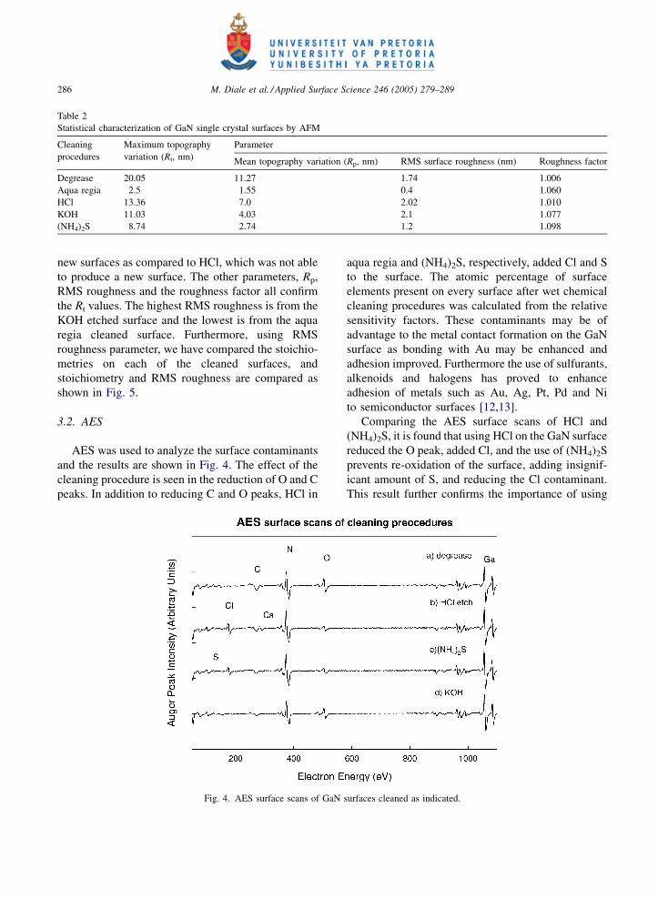
M. Diale et al. / Applied Surface Science 246 (2005) 279–289286
Table 2
Statistical characterization of GaN single crystal surfaces by AFM
Cleaning
procedures
Maximum topography
variation (Rt, nm)
Parameter
Mean topography variation (Rp, nm) RMS surface roughness (nm) Roughness factor
Degrease 20.05 11.27 1.74 1.006
Aqua regia 2.5 1.55 0.4 1.060
HCl 13.36 7.0 2.02 1.010
KOH 11.03 4.03 2.1 1.077
(NH4)2S 8.74 2.74 1.2 1.098
new surfaces as compared to HCl, which was not able
to produce a new surface. The other parameters, Rp,
RMS roughness and the roughness factor all confirm
the Rt values. The highest RMS roughness is from the
KOH etched surface and the lowest is from the aqua
regia cleaned surface. Furthermore, using RMS
roughness parameter, we have compared the stoichio-
metries on each of the cleaned surfaces, and
stoichiometry and RMS roughness are compared as
shown in Fig. 5.
3.2. AES
AES was used to analyze the surface contaminants
and the results are shown in Fig. 4. The effect of the
cleaning procedure is seen in the reduction of O and C
peaks. In addition to reducing C and O peaks, HCl in
Fig. 4. AES surface scans of GaN
aqua regia and (NH4)2S, respectively, added Cl and S
to the surface. The atomic percentage of surface
elements present on every surface after wet chemical
cleaning procedures was calculated from the relative
sensitivity factors. These contaminants may be of
advantage to the metal contact formation on the GaN
surface as bonding with Au may be enhanced and
adhesion improved. Furthermore the use of sulfurants,
alkenoids and halogens has proved to enhance
adhesion of metals such as Au, Ag, Pt, Pd and Ni
to semiconductor surfaces [12,13].
Comparing the AES surface scans of HCl and
(NH4)2S, it is found that using HCl on the GaN surface
reduced the O peak, added Cl, and the use of (NH4)2S
prevents re-oxidation of the surface, adding insignif-
icant amount of S, and reducing the Cl contaminant.
This result further confirms the importance of using
surfaces cleaned as indicated.

M. Diale et al. / Applied Surface Science 246 (2005) 279–289 287
Fig. 5. Graph of root mean square (RMS) surface roughness and Ga/N ratio from AES elemental surface concentrations. Ga/N ratio close to 1 is
stoichiometric.
(NH4)2S as a chemical that prevents re-oxidation of
surfaces. KOH removed all the Cl from the surface,
and reduced the C significantly.
There had been reports of improved electrical
characteristics of metals/GaN contacts after treat-
ments in HF, HCl, and NaOH. Miller et al. has
reported the reduction of reverse bias leakage current
in GaN Schottky diodes after treatment in NaOH. The
high concentration of OH-ion on the GaN surface is
attributed to the reduction of reverse bias leakage in
their Schottky contacts [14]. In another report, Lin and
Lee has reported the reduction of surface states on
InGaN using (NH4)2S [15]. Electrically, (NH4)2S was
reported to reduce the Schottky barrier height. In
particular, it was reported that Ga–O, In–O and C–O
bonds were removed from the InGaN surface after
(NH4)2S treatment. Furthermore, repeated exposure of
the surface that has a Cl peak to the electron beam in
the AES system has resulted in desorption of the
surface contaminants, and consequently, complete
removal of the Cl peak.
To further analyse the cleaned surfaces, the ratio of
Ga/N, and RMS surface roughness are plotted as a
function of cleaning method, as shown in Fig. 5. There
is a relationship between the RMS surface roughness
and the contaminants on the surfaces, which conse-
quently affects the Ga/N ratio. The as-grown surface
shows a very high surface roughness and Ga/N ratio
and the cleanest surface shows lowest surface rough-
ness and Ga/N ratio. Therefore as the surface is
cleaned, the surface roughness reduces as the Ga/N
ratio improves, implying that the chemicals used has
etch GaN surface to remove contaminants. The RMS
surface roughness of KOH etched surface, differ from
the as-grown surface by about 0.4 nm. Different wet
chemicals used previously in removing contaminants
on GaN have shown no effect on the surface roughness
of the material [2,3]. The work done previously to etch
and remove surface GaN to form etch steps were not
achieved by using HCl and KOH [16]. Ultraviolet light
illumination and addition of ions were used to etch
GaN successfully in KOH [17].
Previous results have recommended the use of
thermal desorption after every chemical clean, to
completely remove surface contaminants [1–3]. In this
work, we have found that thermal cleaning of the
degreased GaN surface resulted in almost complete
removal of surface contaminants. Fig. 6 is a typical
temperature profile of a sample cleaned in UHV under
high temperatures. This profile may be divided into
two regions: region 1 from 23 to 500 8C and region II
from 500 to 1010 8C. In region I, the carbon peak first

M. Diale et al. / Applied Surface Science 246 (2005) 279–289288
Fig. 6. Surface concentration profiles of O and C on GaN surface during thermal anneal in the AES.
decreases and then increases as temperature increases.
In region II, the carbon coverage on the surface of GaN
decreases until it drops to below AES detection limit,
where average peak-to-peak height is less than 1.5. In
the case of oxygen, the surface coverage starts
increasing and quickly decreases sharply until the
temperature of about 500 8C. At this temperature, all
oxides are removed from the surface according to AES
sensitivity, in which average peak-to-peak height is
less than 0.5. The increase in O from 23 to 50 8C may
be attributed to the removal of common surface water
that had been covering the surface prior to thermal
heating. This water is very sticky and is usually
removed at temperatures above 220 8C. On the other
hand, the increase in C may be due to segregation from
the bulk, which needs further study to confirm.
4. Conclusions
In conclusion, the effectiveness of wet chemical
cleaning of GaN with different solutions, have been
characterized by AFM and AES. AFM results have
shown that GaN surface roughness is affected by the
cleaning method used on the surface. Surface defects
were characterized by different etch chemicals, with
(NH4)2S producing a defect-free interface. AES has
shown the contaminant as C and O and that using
compounds with Cl and S, will leave Cl and S on the
surface. This result has given sufficient information on
removal of surface contamination; stoichiometry;
surface roughness and chemical etch. Using
(NH4)2S prevented re-oxidation of the surface, and
further removes Cl from the surface of the GaN. KOH
effectively removes the C on the surface. The effects
of S and Cl on the surface may enhance adhesion of
metals to GaN surface, thus improving device quality.
Further work is necessary in finding the effects of
different cleaning procedures on the optical properties
of the material and electrical properties of devices.
Acknowledgements
The National Research Foundation, the University
of Pretoria and the University of Free State funded the
project.
References
[1] L.L. Smith, S.W. King, R.J. Nemanich, R.F. Davis, J. Electron.
Mater. 25 (1996) 805.
[2] S.W. King, J.P. Barnak, M.D. Bremster, K.M. Tracey, C.
Ronning, R.F. Davis, R.J. Nemanich, J. Appl. Phys. 84
(1998) 5248.
[3] K.N. Lee, S.M. Donovan, B. Gila, M. Overberg, J.D. Mack-
enzie, C.R. Abernathy, R.G. Wilson, J. Electro. Chem. Soc.
147 (2000) 3087.

M. Diale et al. / Applied Surface Science 246 (2005) 279–289 289
[4] C.M. Pelto, Y.A. Chang, Y. Chen, R.S. Williams, Solid State
Electron. 45 (2001) 1597.
[5] F. Machuca, Z. Liu, Y. Sun, P. Pianetta, W.E. Spicer, R.F.
Pease, J. Vac. Sci. Technol. A 20 (2002) 1784.
[6] R.J. Shul, G.A. Vawter, C.G. Willison, J.W. Lee, S.J. Pearton,
C.R. Abernathy, Solid Stat. Electron. 42 (1998) 2259.
[7] J.M. Nel, C.M. Demanet, K.T. Hillie, F.D. Auret, H.L. Gaiger,
Appl. Surf. Sci. 134 (1998) 22.
[8] P.N.K. Deenapanray, F.D. Auret, G. Myburg, K.T. Hillie, C.M.
Demanet, Surf. Interf. Anal. 26 (1998) 748.
[9] J. Jasinki, W. Swider, Z. Liliental-Werber, P. Visconti, K.M.
Jones, M.A. Reshchikov, F. Yun, H. Morkoc, S.S. Park, K.Y.
Lee, Appl. Phys. Lett. 78 (2001) 2297.
[10] H. Morkoc, Mat. Sci. Eng. R33 (2001) 135.
[11] D. Zymierska, J. Auleytner, T. Kobiela, R. Dus, Phys. Solid
State (a) 180 (2000) 479.
[12] J. Wang, B. Zeng, C. Fang, X. Zhou, J. Electroanal. Chem. 484
(2000) 88.
[13] I. Shalish, Y. Shapira, L. Burstein, J. Salzan, J. Appl. Phys. 89
(2001) 390.
[14] E.J. Miller, D.M. Schaadt, E.T. Yu, P. Walterit, C. Poblenz, J.S.
Speck, Appl. Phys. Lett. 82 (2003) 1293.
[15] Y.-J. Lin, C.-T. Lee, J. Vac. Sci. Technol. B 9 (2001)
1734.
[16] C.B. Vartuli, S.J. Pearton, C.R. Abernathy, J.D. Mackenzie, F.
Ren, Solid State Electron. 41 (1997) 1947.
[17] D.A. Stocker, E.F. Schubert, J.M. Redwing, Appl. Phys. Lett.
73 (1998) 2654.

ARTICLE IN PRESS
Physica B 404 (2009) 4415–4418
Contents lists available at ScienceDirect
Physica B
0921-45
doi:10.1
Corr
E-m
journal homepage: www.elsevier.com/locate/physb
Effects of chemical treatment on barrier height and ideality factors of Au/GaNSchottky diodes
M. Diale , F.D. Auret
Department of Physics, University of Pretoria, Lynwood Road, Pretoria 0002, South Africa
a r t i c l e i n f o
PACS:
73.30.+y
79.40.+z
Keywords:
Surface treatment
Schottky contact
26/$ - see front matter & 2009 Elsevier B.V. A
016/j.physb.2009.09.039
esponding author. Tel.: +27 12 420 4418; fax:
ail address: [email protected] (M. Dia
a b s t r a c t
We have studied Au/n-GaN Schottky barrier diodes. GaN surfaces have been prepared by cleaning in HCl
and (NH4)2S prior to metal deposition. The zero-biased barrier heights and ideality factors obtained
from the current–voltage characteristics differ from diode to diode, although all the samples were
prepared identically. The statistical analysis for the reverse bias C–V data yielded mean value of
(1.3570.04) eV for Schottky barrier height of HCl treated sample and (1.2070.03) eV for (NH4)2S
sample, where 9 dots were considered from each cleaning method. It was found that the barrier height
values obtained from the C2–V (1.43 eV) and I–V characteristics (0.89 eV) are different from each other
by 0.54 eV. The inhomogeneous barrier heights were found to be related to the effect of the high series
resistance on diode parameters (Akkilic- et al., 2004) [1].
& 2009 Elsevier B.V. All rights reserved.
1. Introduction
Rectifying contacts with low leakage currents and high barrierheight are required for the successful fabrication of GaN-baseddevices. Schottky barrier diodes (SBD) are the choice structure formany semiconductor devices, including microwave diodes, field-effect transistors and photodiodes [2–4]. Their technologicalimportance requires a full understanding of the nature of theelectrical characteristics of SBDs. It is well known that SBD has athin layer of an oxide between the metal and the semiconductor,which cannot be removed by conventional chemical cleaning.Such an oxide converts the diode to metal–insulator–semicon-ductor (MIS) and usually influences the electrical characteristicsof the diode, causing a change in the interfacial charge with bias,giving rise to an electric field at the interfacial layer between themetal and the semiconductor [5,6]. The oxide layer reduces thebarrier height and consequently increases the series resistance.
Generally, the forward biased current–voltage (I–V) character-istics are linear in the semi-logarithmic scale at low voltages, butdeviate considerably from linearity due to the effects of seriesresistance, Rs resulting from the presence of the thin oxide layerand other surface contaminants. The series resistance is onlyeffective in the curvature downward region or non-linear regionof the forward I–V characteristics at sufficiently high voltages.The concavity of the current–voltage characteristics at highervoltages increases with increasing series resistance. Increasingseries resistance decreases the barrier height and this result in
ll rights reserved.
+27 12 362 5288.
le).
non-ideal current–voltage characteristics. Other parameters suchas the ideality factor, n(V) and zero bias barrier height, Fb;0 areeffective in both the linear and the non-linear regions of the I–V
curve, accompanying the changes in the Schottky barrier height(SBH) [7]. The effect of the series resistance between the depletionregion and the ohmic contact of the neutral region of thesemiconductor bulk causes the I–V characteristics of the metal–semiconductor contact to deviate from the expected [8].
The interface states at the metal–semiconductor junction playa vital role in evaluating the Schottky barrier height and theideality factor. These manifest themselves as deviations from theideal Schottky barrier formation and are localized within a fewatomic layers of the intimate metal–semiconductor contact withenergies which fall inside the forbidden gap. Bardeen showed thatsuch charge accumulated at the metal–semiconductor contactreduces the effective potential difference between the semicon-ductor and the metal contact [9]. Interface states arise fromsemiconductor surface states due to discontinuity in the latticepotential, metal-induced-gap states due to wave-function tunnel-ing from the metal into the semiconductor, surface states due tocontamination and defects; and any new compounds formed as aresult of the interaction of the metal and the semiconductor.
A study of the importance of series resistance in calculating thecharacteristic parameters of Si Schottky contacts was done byAydin et al. [1], obtaining their estimations from determination ofinterface states density distribution from the analysis of thecurrent–voltage measurements. Kampen and Monch studied thebarrier heights of different metals on GaN using metal-inducedgap states (MIGS) and the electronegativity model, concludingthat the experimental values of the barrier height are excellentlyreproduced by the theoretical predictions, which follow from

ARTICLE IN PRESS
M. Diale, F.D. Auret / Physica B 404 (2009) 4415–44184416
physical MIGS and the electronegativity concept [10]. A review ofmetal-contact technology has revealed the importance of surfacepreparation prior to metal deposition [11]. In this study, twodifferent surface chemicals were used to treat GaN surface prior tometal deposition. The effects of chemical treatments on Schottkycharacteristics were investigated using capacitance–voltage (C–V)and current–voltage (I–V) characteristics. The average barrierheight for the diodes was 1.43 and 1.20 eV for C–V; and 0.81 and0.89 for I–V measurements, respectively.
2. Experimental
For this investigation, we have used GaN samples with carrierdensity of 11017 cm3, obtained from TDI. Before contactfabrication, samples were cleaned using trichloroethylene (TEC),Isopropanol and HCl:HNO3 aquaregia. Each of these samples wasfinally etched in 1:1 HCl:H2O (sample 1) and (NH4)2S (sample 2),respectively. Using patterned surface, Ti/Al/Ni/Au (150/2200/400/500 A) ohmic contacts were deposited by electron-beam andannealed in ultra pure Ar for 5 min at 500 1C. Thereafter, AuSchottky contacts, 0.25 mm thick, were deposited in the resistiveevaporator at room temperature. The values of zero-biased barrierheight and ideality factor were determined from I–V and C–V
measurements at room temperature and corrected afterwards forthe effect of series resistance.
3. Results and discussion
In Schottky diodes, the depletion layer capacitance can beexpressed as [2]
C2 ¼2ðVbi VAÞ
qesA2NDð1Þ
where A is the area of the diode, Vbi the diffusion potential at zerobias and is determined from the extrapolation of the linear C2
V plot to the V axis and VA is the applied voltage. The value of thebarrier height can be obtained from the relation:
Fb;0ðC VÞ ¼ VbiþV0 ð2Þ
Fig. 1. Reverse bias C2–V curves of the HCl and (NH4)2S samples. For these particular di
where V0 is the potential difference between the bottom of theconduction band and the Fermi level; and can be calculatedknowing the donor concentration ND obtained from the followingrelation:
V0 ¼ ðkTÞlnNC
ND
ð3Þ
where NC ¼ 4:6 1016 cm3 is the effective density of states in theconduction band [3].
Nine dots with the same diameter (0.25 mm) on eachsample were evaluated. Fig. 1 shows the reverse bias C2 V
characteristics for one diode from sample 1 and sample 2,respectively. For these particular diodes on samples 1 and 2, theC–V barrier heights are 1.43 and 1.20 eV, respectively. The carrierconcentration of 1.91016 and 2.41016 cm3 from the reversebias C2 V plots was obtained for samples 1 and 2. The C–V
barrier heights ranged from 1.28 to 1.50 eV for sample 1 and from1.14 to 1.25 eV for sample 2. The statistical analysis for the C–V
data yielded SBH mean value of 1.3570.04 eV for sample 1 dotsand SBH mean value of 1.2070.03 eV for sample 2.
In Schottky barrier diodes, the barrier height depends onthe voltage and surface conditions prior to metal deposition. Thesurface condition includes the thickness of the interfacial oxide,which affects the current–transport mechanisms. These includethe thermionic emission, which is characterized by idealityclose to unity and thermionic field emission and field emission.These mechanisms are affected by series resistance, tunneling andgeneration recombination in the depletion region. Table 1 givesthe summary of the electrical characteristics of the diodes.
For a Schottky contact with series resistance, the net current ofthe device is due to thermionic emission and it is written as [2]
I¼ I0exp qðVA IRsÞ
nkT
ð4Þ
where the saturation current, I0 is expressed as
I0 ¼ AAT2exp qFb;0
kT
ð5Þ
where q is the electron charge, A is the effective Richardsonconstant and is equal to 26 A/cm2 K2 for n-type GaN [12], A is the
odes on samples 1 and 2, the C–V barrier heights are 1.43 and 1.20 eV, respectively.

ARTICLE IN PRESS
M. Diale, F.D. Auret / Physica B 404 (2009) 4415–4418 4417
diode area, T is the absolute temperature, k Boltzmann constant, n
the ideality factor of the SBD and Fb:0 the zero bias barrier height.When VAZ3kT=q, the extrapolated current, I0 and the zero biasbarrier height can be expressed as
Fb;0 ¼kT
qln
AAT2
I0
ð6Þ
and the ideality factor from Eq. (4) can be written as
n¼q
kT
dV
dðln IÞð7Þ
The ideality factor of the SBD, n is a measure of the conformity ofthe diode to pure thermionic emission. From Fig. 2, current–transport mechanisms displayed are thermionic emission and theseries resistance effect at high voltages. The values of the idealityfactor, n and the barrier height, Fb were calculated from theforward I–V characteristics according to Eqs. (6) and (7). Forsample 1 the barrier height, Fb:0 ranged from 0.79 to 0.89 eV andthe ideality factor n ranged from 1.02 to 1.17. Sample 2 Fb:0 valuesranged from 0.71 to 0.85 eV and the n from 1.31 to 1.36.The statistical analysis yielded mean values of 0.8470.05 eV forthe 1.0670.50 for barrier height and ideality factor of sample 1(9 dots), respectively, and the mean values of 0.8070.01 eVand 1.3470.20 (9 dots) for sample 2 diodes. Ideality factors
Fig. 2. The I–V curves of the treated samples. The series resistance values of HCl samples
reduced barrier height.
Table 1Values obtained experimentally from the current–voltage characteristics of the
Au/GaN Schottky diodes.
Sample 1
n 1.17
Rs (O) 22.3
Fb,c (eV), C–V 1.43
Fb,0 (eV), I–V 0.82
Sample 2
n 1.89
Rs (O) 17.1
Fb,c (eV), C–V 1.20
Fb,0 (eV), I–V 0.71
The difference in series resistance for the samples 1 and 2 is due to the surface
state after different chemical treatment.
above unity has been attributed to interface states due to thinoxide layer between the metal and the semiconductor, includingother contaminants, tunneling currents in highly doped semi-conductors, image-force lowering of the Schottky barrier inelectric field at the interface and generation-recombinationcurrents within the depletion region [2]. Our previous resultshave shown S and Cl residues onto GaN after cleaning in HCl and(NH4)2S using Auger electron spectroscopy (AES) and X-rayphotoelectron spectroscopy (XPS) [13]. The work done on GaAsand GaP nitridation has shown anion exchange where a thin layerof Ga–N was formed on each of the materials [14]. Surface Ga–N inturn passivates the GaAs and GaP, affecting the I–V and C–V
characteristics of these materials. In addition, the work done byLiu et al. has shown that the Ga peak becomes larger whensamples are cleaned in (NH4)2S than in HF/HCl [15]. Furthermore,(NH4)2S has been found to reduce the barrier height on GaN, andpreventing re-oxidation of the surface [16]. We suggest that thereexist Ga–Cl and Ga–S on sample 1 and sample 2, respectively.Previous XPS results have shown that as-grown GaN surface hasoxides in the form of Ga2O3 and GaOH. In addition, while rinsingGaN in water, addition of OH to GaN to form the GaOH, may occur,and be part of sticking surface water that may contribute tointerface states [17].
The values of Rs and Fb:0 for both samples 1 and 2 wereobtained as 0.82 eV and 22.3O; and 0.71 eV and 17.0O, respec-tively. As mentioned above, the barrier height values of 1.43 and1.20 eV for samples 1 and 2 were obtained from the C2–V plots,respectively. These barrier height values obtained from the C2–V
(1.43 eV) and I–V characteristics (0.89 eV) are different from eachother by 0.54 eV. We attribute the difference between the I–V andC–V barrier height in the metal–semiconductor to SBH inhomo-geneity. This is the fact that the barrier heights of the diodes onthe same sample differs from diode to diode and at differentpositions on the same diode. The measured I–V barrier height issignificantly lower than the weighted arithmetic average of theSBHs. On the other hand, the C–V measured barrier height isinfluenced by the distribution of charge at the depletion regionfollows the weighted arithmetic average of the barrier heightinhomogeneity; hence the BH determined by C–V is close to theweighted arithmetic average of the barrier heights. Therefore, the
are generally higher than those treated in (NH4)2S, which presented less oxide and

ARTICLE IN PRESS
M. Diale, F.D. Auret / Physica B 404 (2009) 4415–44184418
barrier height determined from zero bias intercept assumingthermionic emission as current transport mechanism is wellbelow the measured BH and the weighted arithmetic average ofthe barrier heights [18,19]. Furthermore, the surface damage atthe metal–semiconductor interface affects the I–V measurementsbecause defects may act as recombination centers for trap-assisted tunneling currents. C–V measurements are generally lessprone to interface states, so that the determined barrier height isconsidered more reliable, though the depletion width can bealtered by the interface defects if they are deeper into the spacecharge region [20].
4. Summary
In conclusion, we have fabricated Au/n-GaN SBDs usingdifferent cleaning procedures. From the current–voltage charac-teristics, we obtained the values of ideality factor, SBH and Rs forthe samples. The I–V characteristics are near ideal with thermio-nic emission as the dominant current transport mechanism.Furthermore, HCl treated samples behave like a MIS diode due tothe amount of oxide remaining on the surface after treatment.The series resistance values of HCl samples are generally higherthan those treated in (NH4)2S, which presented less oxide andreduced barrier height, in agreement with published results. Mostpublished results on GaN have only reported their findingswithout specifics on current transport mechanism. Thus furtherwork is needed for the investigation ideality factor far above unity,which will need the knowledge of the oxide layer thickness onGaN, effects of passivation of GaN surface on electrical character-istics, and analysis of barrier height inhomogeneities on therectifying diode characteristics on GaN.
Acknowledgment
The authors gratefully acknowledge financial assistance fromthe South African National Research Foundation.
References
[1] K. Akkilic- , M.E. Aydin, A. Turut, Physica Scripta 70 (2004) 364.[2] E.H. Rhoderick, R.H. Williams, Metal–Semiconductor Contacts, Clarendon
Press, Oxford, 1988.[3] S.M. Sze, Physics of Semiconductor Devices, second ed., Wiley, New York,
1981.[4] L. Wang, M.I. Nathan, T.-H. Lim, M.A. Khan, Q. Chen, Applied Physics Letters 68
(9) (1996) 1267.[5] P. Hanselaer, W.H. Laflere, R.L. Meirhaeghe, F. Cardon, Applied Physics Letters
56 (1984) 2309.[6] E. Monroy, F. Calle, J.L. Pau, E. Mu noz, F. Omnes, Electronic Letters 36 (25)
(2000) 2096.[7] J.C. Card, E.H. Rhoderick, Journal of Applied Physics D 4 (1971) 1589.[8] M.E. Aydin, K. Akkilic- , T. Kilic-o
˘glu, Applied Surface Science 225 (2004) 1304.
[9] J. Bardeen, Physical Review 71 (1947) 771.[10] T.U. Kampen, W. Monch, Applied Surface Science 117/118 (1997) 388.[11] Q.Z. Liu, S.S. Lau, Solid State Electronics 42 (1998) 677.[12] A.C. Schmidt, A.T. Ping, M. Asif Khan, Q. Chen, J.W. Yang, I. Adesida,
Semiconductor Science and Technology 11 (1996) 1464.[13] M. Diale, F.D. Auret, N.G. van der Berg, R.Q. Odendaal, W.D. Roos, Applied
Surface Science 246 (2005) 279.[14] G. Bruno, Applied Surface Science 235 (2004) 239.[15] J. Liu, B. Shen, Y.G. Zhou, H.M. Zhou, M.J. Wang, Z.W. Zheng, B. Zhang, Y. Shi,
Y.D. Zheng, Optical Materials 23 (2003) 133.[16] X.A. Cao, S.J. Pearton, G. Dang, A.P. Zhang, F. Ren, J.M. Van Hove, Applied
Physics Letters 75 (1999) 4130.[17] M. Diale, F.D. Auret, N.G. van der Berg, R.Q. Odendaal, W.D. Roos, Surface and
Interface Analysis 37 (2005) 1158.[18] J.H. Werner, H.H. Guttler, Journal of Applied Physics 69 (3) (1991) 1552.[19] R.T. Tung, A.F.J. Levi, J.P. Sullivan, F. Schrey, Physical Review Letters 66 (1)
(1971) 72.[20] C. Fontaine, T. Okumura, K.N. Tu, Journal of Applied Physics 54 (1983) 1404.