scanning probe microscopy studies of pbs surfaces … · dtd 5 scanning probe microscopy studies of...
TRANSCRIPT

DTD 5
www.elsevier.com/locate/apsusc
Applied Surface Science xxx (2005) xxx–xxx
Scanning probe microscopy studies of PbS surfaces oxidized
in air and etched in aqueous acid solutions
Yuri L. Mikhlin *, Alexander S. Romanchenko, Alexander A. Shagaev
Institute of Chemistry and Chemical Technology SB RAS, K. Marx Street, 42, Krasnoyarsk 660049, Russia
Received 10 February 2005; received in revised form 9 July 2005; accepted 9 July 2005
Abstract
Natural n-type PbS single crystals have been studied using AFM, STM and STS after long-term oxidation in air at ambient
temperatures and extensive etching in aqueous acid solutions, in contrast to previous work devoted to initial corrosion of fresh
surfaces. The exposure of PbS to atmosphere at high relative humidity for several days yields widespread loose oxidation
products; the process is much slower at low humidity. Surface morphologies diverge after the treatment in 1 M perchloric and
hydrochloric acid solutions at room temperature and become widely different at elevated temperatures, displaying commonly
etch pits up to several micrometers in size and depth along with rather uniformly distributed 20–100 nm protrusions of PbS
phase. The changes both in topography and semiconducting properties of PbS found by tunneling spectroscopy have been
explained in terms of the non-uniform distribution of donor- and acceptor-type defects D+/D� in the metal depleted surface
layer, which are generated by chemical reactions and, in turn, determine the rates of the PbS corrosion. In particular, the D�
centers exhibit a self-catalyzing effect on the non-oxidative local dissolution of PbS in HCl media, resulting in the deep etch pits.
# 2005 Elsevier B.V. All rights reserved.
Keywords: Lead sulfide; Oxidation; Acidic dissolution; Scanning probe microscopy; Tunneling spectroscopy; Surface topography
1. Introduction
Lead sulfide (PbS, galena) is the major ore mineral
of lead and is applied in infrared detectors as a
semiconductor with the band gap of about 0.4 eV [1,2].
Furthermore, PbS nanoparticles attract much attention
due to strong confinement effects on electrons and
phonons [2]. The surface characteristics and reaction
* Corresponding author. Tel.: +7 3912 494885;
fax: +7 3912 238658.
E-mail address: [email protected] (Y.L. Mikhlin).
0169-4332/$ – see front matter # 2005 Elsevier B.V. All rights reserved
doi:10.1016/j.apsusc.2005.07.009
mechanisms for PbS oxidation in air and aqueous
solutions are important for mineral processing,
geochemistry, and the production, performance and
degradation of optoelectronic devices. Conditioning in
aqueous acidic solutions represents a standard etching
procedure for II–VI and IV–VI semiconductors and
a prospective process of hydrometallurgical recovery
of lead. Consequently, lead sulfide surfaces have been
extensively studied in order to understand their
composition, structure and properties, to specify
products and to gain an insight into the reaction
mechanisms (see, e.g., [1,3–8] and references herein).
.
APSUSC-13015; No of Pages 14

Y.L. Mikhlin et al. / Applied Surface Science xxx (2005) xxx–xxx2
DTD 5
Apart from elemental sulfur and oxygen-containing
compounds of lead and sulfur (PbO, Pb(OH)2, PbSO4,
etc.), X-ray photoelectron spectroscopy (XPS) exam-
ination of a variety of reacted surfaces revealed
considerable depletion of the sulfidic phase in metal
due to more rapid release of Pb during PbS interaction
with air and aqueous solutions [4,8–14]. It was also
found that PbS reactivity strongly depends on anionic
composition of acid solutions [12,13]. Basing on XPS,
X-ray spectroscopy, scanning electron microscopy
(SEM), dissolution kinetics and electrochemistry
studies, we have proposed recently [8,12,13] to describe
such non-stoichiometric disordered layers of PbS and
other metal sulfides in much the same way as non-
crystalline semiconducting chalcogenides, which spe-
cial properties are thought to be due to the presence and
non-uniform distribution of plentiful defects having
negative correlation energy (Hubbard energy) [15,16].
A number of researchers employed scanning probe
microscopy (SPM) to examine PbS surfaces [17–32].
Eggleston and Hochella [17–21] found using scanning
tunneling microscopy (STM) and tunneling spectro-
scopy (STS) that PbS oxidation in air and under oil is
non-uniform and probably autocatalytic, showing a
decreased brightness of S sites in areas with [1 1 0]-
parallel borders. Tunneling spectra taken in air were
indicative of the gap width of about 0.25 eVand n-type
conductivity of the semiconductor surface [18–20];
they are dissimilar to calculated spectra [22–24].
Several STM studies in air [25,26] and aqueous systems
[27,28] showed the protrusions composed of oxidation
products, which were randomly scattered on natural
galena but were preferentially located on terrace steps at
synthetic specimens, suggesting that the oxidation
starts at impurities and crystal defects. Wittstock et al.
[29] observed using in situ atomic force microscopy
(AFM) a roughening of the surface ascribed to non-
oxidative galena dissolution in acetate buffer (pH 4.9)
and then, at anodic potentials, two types of protrusions
formed by sulfur, which differed in the size and mutual
distances. Higgins and Hamers found by in situ STM
that both electrochemical oxidation and reduction in
oxygen-depleted perchlorate solutions (pH 1.7) [30],
and acidic dissolution of galena in sulfate media (pH 2.7
and 7) [31] proceed via removal of material from step
edge and are fastest along the [1 0 0] directions.
Moreover, impurity-related defects were considered to
entail etch pit development at terraces under oxidizing
conditions. De Giudici and Zuddas [32] performed an in
situ AFM investigation of galena dissolution in air-
saturated HCl solutions (pH 1 and 3) over 45 h. Square
etch pits reached a depth of 80 nm in first hours, and
then nucleation and growth of new etch pits was
inhibited, possibly due to homogeneously distributed
protrusions 1–3 nm high, so large rough terraces
delimited by macrosteps 50–100 nm high were formed.
The authors concluded that the protrusions were
composed of elemental sulfur, the dissolution of which
(as oxysulfur anions) represents the rate-limiting step of
the overall process. Most recently, Cama et al. [33]
reported the results of non-stirred flow-through kinetics
experiments, in situ and ex situ AFM, and XPS surface
analysis of galena reacted in hydrochloric acid solutions
(pH 1–3) at 20–25 8C, which agreed with the
dissolution mechanisms suggested in Ref. [32].
Furthermore, the ex situ tapping mode images show
the growth of larger protrusions of sulfur and lead
sulfate on galena substrate at acidic pH, particularly in
more oxidative media containing HNO3 instead HCl or
Fe3+ ions.
It is worth emphasizing that the chemical reactions
were conducted at room temperature in all the SPM
studies cited above, and they mostly dealt with initial
stages of PbS corrosion. There is a need, however, to
understand longer-term metal sulfide corrosion rather
than just initial corrosion of fresh surfaces. In the
current paper, we report scanning probe microscopic
images and tunneling spectra of natural PbS single
crystal surfaces oxidized in air for long periods or
substantially modified in aqueous acidic solutions.
The images were recorded ex situ in order to conduct
the chemical treatment under fairly severe conditions.
The acidic etching was found to pattern the reacted
surfaces simultaneously in nano- and micrometer
scales and to modify semiconducting characteristics,
differently in various solutions. These results shed new
light on mechanisms of the metal sulfide reactivity and
open up possibilities for creation of premeditated
surface topographies.
2. Experimental
Single crystals of natural galena obtained from
Geological Museum of Central Siberia had less than
0.1% by mass of metal impurities and no inclusions of
Y.L. Mikhlin et al. / Applied Surface Science xxx (2005) xxx–xxx 3
DTD 5
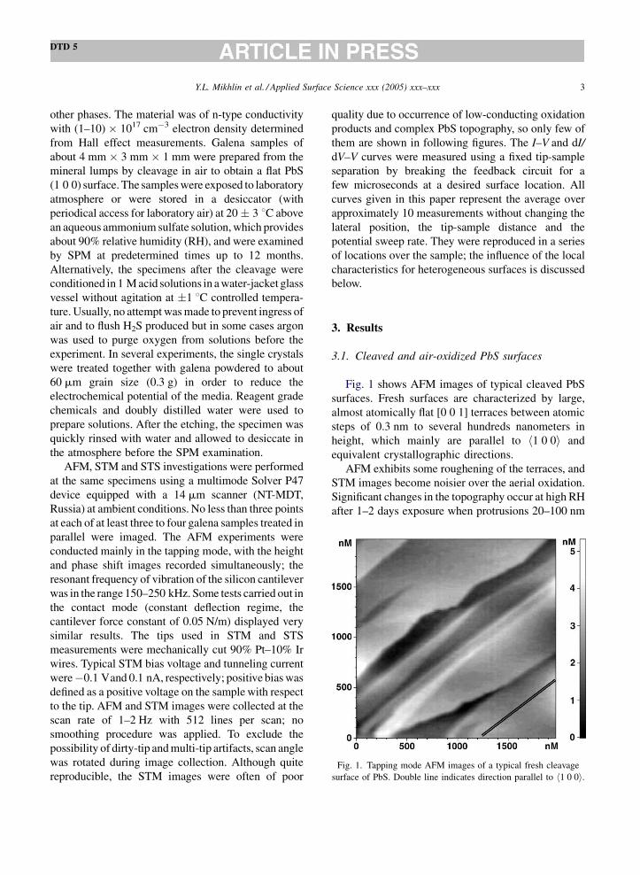
Fig. 1. Tapping mode AFM images of a typical fresh cleavage
surface of PbS. Double line indicates direction parallel to h1 0 0i.
other phases. The material was of n-type conductivity
with (1–10) � 1017 cm�3 electron density determined
from Hall effect measurements. Galena samples of
about 4 mm � 3 mm � 1 mm were prepared from the
mineral lumps by cleavage in air to obtain a flat PbS
(1 0 0) surface. The samples were exposed to laboratory
atmosphere or were stored in a desiccator (with
periodical access for laboratory air) at 20 � 3 8C above
an aqueous ammonium sulfate solution, which provides
about 90% relative humidity (RH), and were examined
by SPM at predetermined times up to 12 months.
Alternatively, the specimens after the cleavage were
conditioned in 1 M acid solutions in a water-jacket glass
vessel without agitation at �1 8C controlled tempera-
ture. Usually, no attempt was made to prevent ingress of
air and to flush H2S produced but in some cases argon
was used to purge oxygen from solutions before the
experiment. In several experiments, the single crystals
were treated together with galena powdered to about
60 mm grain size (0.3 g) in order to reduce the
electrochemical potential of the media. Reagent grade
chemicals and doubly distilled water were used to
prepare solutions. After the etching, the specimen was
quickly rinsed with water and allowed to desiccate in
the atmosphere before the SPM examination.
AFM, STM and STS investigations were performed
at the same specimens using a multimode Solver P47
device equipped with a 14 mm scanner (NT-MDT,
Russia) at ambient conditions. No less than three points
at each of at least three to four galena samples treated in
parallel were imaged. The AFM experiments were
conducted mainly in the tapping mode, with the height
and phase shift images recorded simultaneously; the
resonant frequency of vibration of the silicon cantilever
was in the range 150–250 kHz. Some tests carried out in
the contact mode (constant deflection regime, the
cantilever force constant of 0.05 N/m) displayed very
similar results. The tips used in STM and STS
measurements were mechanically cut 90% Pt–10% Ir
wires. Typical STM bias voltage and tunneling current
were�0.1 Vand 0.1 nA, respectively; positive bias was
defined as a positive voltage on the sample with respect
to the tip. AFM and STM images were collected at the
scan rate of 1–2 Hz with 512 lines per scan; no
smoothing procedure was applied. To exclude the
possibility of dirty-tip and multi-tip artifacts, scan angle
was rotated during image collection. Although quite
reproducible, the STM images were often of poor
quality due to occurrence of low-conducting oxidation
products and complex PbS topography, so only few of
them are shown in following figures. The I–V and dI/
dV–V curves were measured using a fixed tip-sample
separation by breaking the feedback circuit for a
few microseconds at a desired surface location. All
curves given in this paper represent the average over
approximately 10 measurements without changing the
lateral position, the tip-sample distance and the
potential sweep rate. They were reproduced in a series
of locations over the sample; the influence of the local
characteristics for heterogeneous surfaces is discussed
below.
3. Results
3.1. Cleaved and air-oxidized PbS surfaces
Fig. 1 shows AFM images of typical cleaved PbS
surfaces. Fresh surfaces are characterized by large,
almost atomically flat [0 0 1] terraces between atomic
steps of 0.3 nm to several hundreds nanometers in
height, which mainly are parallel to h1 0 0i and
equivalent crystallographic directions.
AFM exhibits some roughening of the terraces, and
STM images become noisier over the aerial oxidation.
Significant changes in the topography occur at high RH
after 1–2 days exposure when protrusions 20–100 nm

Y.L. Mikhlin et al. / Applied Surface Science xxx (2005) xxx–xxx4
DTD 5
Fig. 2. Three-dimensional AFM images of air-oxidized PbS. (a)
Contact mode image of the PbS surface exposed to the atmosphere
(RH 90%) for 3 days. A heap formed by the products shifted by the
cantilever and a fracture step (in the right top corner of the image)
are seen. Tapping mode images (b and c) of the PbS surfaces aged in
the laboratory air for 6 months. The figure (b) illustrates the
formation of pits and product accumulations on the oxidized sur-
faces. In figure (c), tracks nearly parallel to the image borders are
produced by submicrodrops of condensed water.
in diameter and 5–15 nm in height arise first at certain
several micrometer sized areas, and they cover the
entire surface over 3–5 days (Fig. 2). The protrusions
are detectable both in the tapping and contact AFM
modes, but STM displays only their marks on a noisy
background. The material making up the protrusions is
loose and can be easily moved by a cantilever impact
(Fig. 2a); they coalesce producing up to a few
micrometers large piles and thin irregular coatings
after 7–10 days. The oxidation is much slower and,
aside from a small roughening, noticeable products
appear on the galena surfaces in laboratory air with 40–
60% RH after the exposure times of 2–3 weeks. The
PbS ageing for several months results in irregular
surfaces exhibiting a nanometer-scale roughness, pits
few nanometers deep and 30–100 nm in diameter, and
accumulations of the solid products (Fig. 2b). For
samples exposed to the laboratory air with RH varied
from 60 to 100% for several summer months (Fig. 2c),
typical are submicrometer-wide tracks formed prob-
ably by microdrops of condensed water, which runs
transferred the covering products.
Rinsing of the oxidized specimens with water
removes most of the oxidation products, but leaves
nanometer-scale traces of the accumulations (not
shown in figures). All the products actually are not
observable in STM images, which are clearer than
those from the samples exposed to the humid
atmosphere for several days but are still noisy.
Previous works [3–13,18–22] have shown that the
oxidation products that accumulate on PbS surface
under similar conditions are composed of elemental
sulfur, lead oxide, lead hydroxide and, in lesser
amounts, lead sulfates and carbonates. Water adsorbed
and condensed on the surface promotes the PbS
oxidation and then wets and renders the product
morphology. It is also evident that the PbS corrosion
begins with and is localized to a considerable degree in
spatial spots, which are randomly scattered or, if the
oxidation rate is fast enough as in the humid air, quite
uniformly distributed over the surface.
3.2. PbS surfaces etched in perchloric acid
solutions
Initial stages of the PbS etching in 1 M HClO4 (in
particular, at room temperature during 10 min)
produce steps oriented largely along the equivalent
Y.L. Mikhlin et al. / Applied Surface Science xxx (2005) xxx–xxx 5
DTD 5
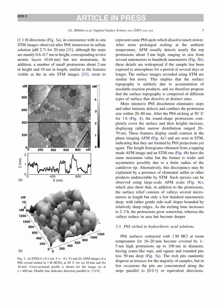
[1 1 0] directions (Fig. 3a), in consistence with in situ
STM images observed after PbS immersion in sulfate
solution (pH 2.7) for 20 min [31], although the steps
are mainly 0.6–0.7 nm in height, corresponding to two
atomic layers (0.64 nm) but not monatomic. In
addition, a number of small protrusions about 2 nm
in height and 10 nm in length, similar to the features
visible at the in situ STM images [31], seem to
Fig. 3. (a) STM (I = 0.1 nA, V = �0.1 V) and (b) AFM images of a
PbS crystal etched in 1 M HClO4 at 20 8C for (a) 10 min and (b)
30 min. Cross-sectional profile is shown for the image (a) at
y = 400 nm. Double line indicates direction parallel to h1 0 0i.
represent some PbS spots which dissolve much slower.
After more prolonged etching at the ambient
temperature, AFM usually detects nearly flat top
protrusions about 5 nm high, ranging in size from
several nanometers to hundreds nanometers (Fig. 3b);
these details are widespread if the sample has been
exposed to atmosphere for a period of several days or
longer. The surface images recorded using STM are
similar but noisy. This implies that the surface
topography is unlikely due to accumulation of
insoluble reaction products, and we therefore propose
that the surface topography is comprised of different
types of surface that dissolve at distinct rates.
More intensive PbS dissolution eliminates steps
and other intrinsic defects and confines the protrusion
size within 20–80 nm. After the PbS etching at 50 8Cfor 1 h (Fig. 4), the round-shape protrusions com-
pletely cover the surface and their heights increase,
displaying rather narrow distribution ranged 20–
70 nm. These features display small contrast in the
phase imaging AFM (Fig. 4a0) and are seen in STM,
indicating that they are formed by PbS projections yet
again. The height histograms obtained from a tapping
mode AFM image and an STM one (Fig. 4b) have the
same maximum value but the former is wider and
asymmetric possibly due to a finite radius of the
cantilever tip. Alternatively, this discrepancy may be
explained by a presence of elemental sulfur or other
products undetectable by STM. Such species can be
observed using large-scale AFM scans (Fig. 4c),
which also show that, in addition to the protrusions,
the surface relief consists of valleys several micro-
meters in length but only a few hundred nanometers
deep, with rather gentle side-wall slopes bounded by
relatively sharp ridges. As the etching time increases
to 2–3 h, the protrusions grow somewhat, whereas the
valleys reduce in area but become deeper.
3.3. PbS etched in hydrochloric acid solutions
PbS surfaces contacted with 1 M HCl at room
temperature for 10–20 min become covered by 1–
5 nm high protrusions up to 100 nm in diameter,
having crater-like tops, and square and rounded pits
less 50 nm deep (Fig. 5a). The etch pits randomly
disperse at terraces for the majority of samples, but in
few occasions the pits are concentrated along the
steps parallel to [0 0 1] or equivalent directions.

Y.L. Mikhlin et al. / Applied Surface Science xxx (2005) xxx–xxx6
DTD 5
Fig. 4. Two-dimensional tapping-mode AFM images of PbS sample etched in 1 M HClO4 at 50 8C for 1 h (a and a0—height and phase imaging),
(b) typical histograms for the protrusion heights obtained from 1 mm � 1 mm AFM and STM images of the same sample. For the image (c) cross-
sectional profile at y = 4000 nm is given.
The protrusions are about evenly distributed on the
surface and overlap each other as well as the pit walls.
The etching in 1 M HCl at the room temperature for
30 min (Fig. 5b) results in the surface morphology
characterized by rare pits 50–100 nm in depth and two
sorts of protrusions, with bigger ones being 100–
300 nm in size and 20–30 nm high, while others being
two to three times smaller and lower. De Guidici and
Zuddas [32] observed similar surfaces of PbS
interacted with more dilute HCl solutions at 20 8Cfor the time extended to 40 h; the authors believed that
the protrusions are composed of elemental sulfur.
Wittstock et al. [29] also observed two types of sulfur
deposits during anodic oxidation of galena in acetate
buffer solution. In the current study, the protrusions
exhibited considerable contrasts at the phase shift
AFM images (Fig. 5b0) and were also discerned using
STM (not shown), so we doubt whether the protru-
sions are really composed of elemental sulfur or
represent PbS irregularities, or, most likely, both of
them, with thin S0 film covering the sulfidic phase
projections. In all likelihood, the initial interaction
of PbS with air-saturated acid solutions proceeds via
both the non-oxidative mechanism releasing H2S
Y.L. Mikhlin et al. / Applied Surface Science xxx (2005) xxx–xxx 7
DTD 5
Fig. 5. Tapping mode AFM images of PbS etched in 1 M HCl at
20 8C for: (a) 15 min; (b) and (b0) 30 min (height and phase
imaging).
and forming the etch pits and the PbS or/and H2S
oxidation yielding S0, which may passivate the
dissolution [32].
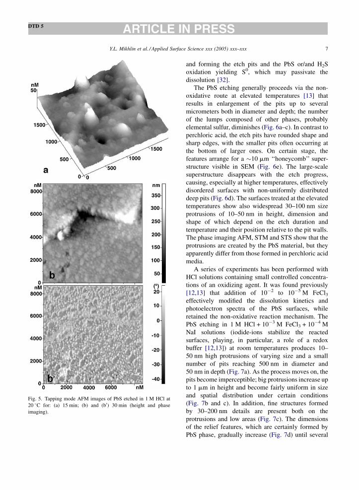
The PbS etching generally proceeds via the non-
oxidative route at elevated temperatures [13] that
results in enlargement of the pits up to several
micrometers both in diameter and depth; the number
of the lumps composed of other phases, probably
elemental sulfur, diminishes (Fig. 6a–c). In contrast to
perchloric acid, the etch pits have rounded shape and
sharp edges, with the smaller pits often occurring at
the bottom of larger ones. On certain stage, the
features arrange for a �10 mm ‘‘honeycomb’’ super-
structure visible in SEM (Fig. 6e). The large-scale
superstructure disappears with the etch progress,
causing, especially at higher temperatures, effectively
disordered surfaces with non-uniformly distributed
deep pits (Fig. 6d). The surfaces treated at the elevated
temperatures show also widespread 30–100 nm size
protrusions of 10–50 nm in height, dimension and
shape of which depend on the etch duration and
temperature and their position relative to the pit walls.
The phase imaging AFM, STM and STS show that the
protrusions are created by the PbS material, but they
apparently differ from those formed in perchloric acid
media.
A series of experiments has been performed with
HCl solutions containing small controlled concentra-
tions of an oxidizing agent. It was found previously
[12,13] that addition of 10�2 to 10�5 M FeCl3effectively modified the dissolution kinetics and
photoelectron spectra of the PbS surfaces, while
retained the non-oxidative reaction mechanism. The
PbS etching in 1 M HCl + 10�3 M FeCl3 + 10�4 M
NaI solutions (iodide-ions stabilize the reacted
surfaces, playing, in particular, a role of a redox
buffer [12,13]) at room temperatures produces 10–
50 nm high protrusions of varying size and a small
number of pits reaching 500 nm in diameter and
50 nm in depth (Fig. 7a). As the process moves on, the
pits become imperceptible; big protrusions increase up
to 1 mm in height and become fairly uniform in size
and spatial distribution under certain conditions
(Fig. 7b and c). In addition, fine structures formed
by 30–200 nm details are present both on the
protrusions and low areas (Fig. 7c). The dimensions
of the relief features, which are certainly formed by
PbS phase, gradually increase (Fig. 7d) until several

Y.L. Mikhlin et al. / Applied Surface Science xxx (2005) xxx–xxx8
DTD 5
Fig. 6. Typical AFM images (height and phase imaging) of PbS surface etched in 1 M HCl: (a, a0) at 30 8C for 30 min, (b, b0) at 50 8C for 30 min,
(c, c0) at 50 8C for 60 min, (d) at 70 8C for 15 min. (e) SEM image of the PbS sample etched in 1 M HCl at 50 8C for 30 min.
Y.L. Mikhlin et al. / Applied Surface Science xxx (2005) xxx–xxx 9
DTD 5
Fig. 7. PbS surfaces etched in 1 M HCl + 10�3 M FeCl3 + 10�4 M NaI: (a) at 20 8C for 20 min, (b) at 50 8C for 10 min, and (c) at 50 8C for
30 min as imaged by STM (a) (I = 0.1 nA, V = �0.1 V) and tapping mode AFM (b and c). (d) Normalized histograms for the protrusion heights
corresponding to the (a)–(c) images.
micrometer sized crystals, probably of lead iodide
irremovable by simple water rinsing, precipitate.
3.4. Tunneling spectra
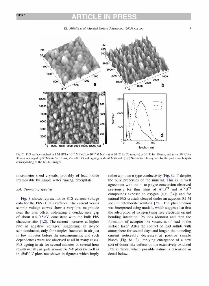
Fig. 8 shows representative STS current–voltage
data for the PbS (1 0 0) surfaces. The current versus
sample voltage curves show a very low magnitude
near the bias offset, indicating a conductance gap
of about 0.4–0.5 eV, consistent with the bulk PbS
characteristics [1,2]. The current increases at higher
rate at negative voltages, suggesting an n-type
semiconductor, only for samples fractured in air just
in few minutes before the measurements, and such
dependences were not observed at all in many cases.
PbS ageing in air for several minutes or several hour
results usually in quite symmetric I–V plots (as well as
in dI/dV–V plots not shown in figures) which imply
rather a p- than n-type conductivity (Fig. 8a, 1) despite
the bulk properties of the mineral. This is in well
agreement with the n- to p-type conversion observed
previously for thin films of AIIBVI and AIVBVI
compounds exposed to oxygen (e.g. [34]) and for
natural PbS crystals cleaved under an aqueous 0.1 M
sodium tetraborate solution [35]. The phenomenon
was interpreted using models, which suggested at first
the adsorption of oxygen tying free electrons or/and
bonding interstitial Pb ions (donors) and then the
formation of acceptor-like vacancies of lead in the
surface layer. After the contact of lead sulfide with
atmosphere for several days and longer, the tunneling
current noticeably decreases at positive sample
biases (Fig. 8a, 2), implying emergence of a new
sort of donor-like defects on the extensively oxidized
PbS surfaces, which possible nature is discussed in
detail below.

Y.L. Mikhlin et al. / Applied Surface Science xxx (2005) xxx–xxx10
DTD 5
Fig. 8. Tunneling spectra of PbS (1 0 0) surfaces: (a) exposed at atmosphere for 1 h (1) and 1 month (2), (b) etched in 1 M HClO4 at 50 8C for
20 min (1) and at 50 8C for 1 h (2), (c) etched in 1 M HCl at 50 8C for 1 h at terraces between the etch pits (1) and at the bottom of the pits (2), (d)
etched in 1 M HCl + 10�3 M FeCl3 + 10�4 M NaI at 20 8C for 20 min (1) and at 50 8C for 30 min (2).
STS plots given in Fig. 8b demonstrate that the
surface formed at the initial stages of the perchloric
acid etching exhibits clear n-type conductivity, and
the samples produced by longer treatment typically
show weak n-type conductivity, indicating the
formation of donor-type defects due to the chemical
treatment.
Tunneling spectra I–V acquired on various PbS
surfaces treated in HCl solutions (Fig. 8c) usually
suggest p-type conductivity. The plots associated with
the etch pit bottoms, especially for the surfaces
obtained under more reductive conditions (in deox-
ygenated solutions or in the presence of PbS powder),
often show peaks at the I–V and dI/dV plots going in
the negative direction (e.g., from +1 to �1 V) at the
negative potentials from �0.1 to �0.3 V. Such kind of
the spectra was well reproduced, as a rule, within 50–
100 nm areas. The peaks can be assigned to very large
density of electronic gap states below the Fermi level,
which have high electron affinity, i.e. acceptors.
The I–V plots measured in the hydrochloric acid
with Fe3+ and I� added notably depend on the
direction of the bias voltage sweep (Fig. 8d). The
etching at 20 8C results in about symmetric curves
suggesting slightly p-type conductivity, with the plots
obtained in the negative-going potential sweep being
somewhat wider. This may be rationalized in terms of
both donor and acceptor gap levels and the Fermi level
pinned in the middle of the gap of the reacted surface
layer, akin to a compensated semiconductor. The
asymmetry and different shifts of the spectra are
evident for the samples etched at higher temperatures;
the positive-going plots indicate usually n-type while
the negative-going ones show obvious p-type surfaces.

Y.L. Mikhlin et al. / Applied Surface Science xxx (2005) xxx–xxx 11
DTD 5
Tunneling spectra differ on various surface spots,
although we failed to establish reliable regularities
between the relief features and the STS characteristics,
except for trivial increase in the tunneling currents
near steep topographic slopes. The STS plots depend
also on the potential sweep rate; this phenomenon
related with impedance measurements, as well as
spatially resolved characteristics and the effect of
voltage sweep direction are worth further examina-
tion.
4. Discussion
4.1. Nature of heterogeneity and defects
While inherent defects in original PbS are most
likely responsible for the spatially non-uniform
corrosion of the material at initial stages [25–31],
the results of the current study suggest that the surface
heterogeneity formed over the prolonged oxidation or
etching is mainly due to defects generated by chemical
reactions. As far back as in late 1950s, Plaksin and co-
workers [36] attributed the effect of oxygen on the
flotation of galena to the formation of acceptor-type
cation vacancies via the reaction
PbS ¼ xPbaq2þ þ Pb1�xS (1)
This hypothesis was later supported by direct mea-
surements of semiconducting characteristics of the
oxidized PbS [34,35] and XPS studies [4,9–14], which
often found the surface depletion in lead over sulfur
beyond the stoichiometry range of the PbS compound.
Furthermore, photoemission spectra of the valence
band and X-ray spectroscopy demonstrated distortions
of chemical bonding in the acid reacted, non-stoichio-
metric layers [12,13], and the above STS findings
suggest a complicated behavior of defect centers
rather than the straightforward formation of acceptor
gap states by lead vacancies.
It was previously proposed [8,12,13,37,38] to
consider the modified, disordered surface layers of
metal sulfides similar to non-crystalline semiconduc-
tors [15,16], using, in particular, the concept of centers
D+/D� having negative correlation energy. These
centers convert one into another when charged
Dþ þ 2e ¼ D� (2)
exhibiting a series of electronic levels in the gap,
energy positions and relative densities of which
depend upon both the Fermi level position and the
rates of the atomic rearrangement after the charge
transfer, with states occupied by one electron being
unstable [15,16]. The mobility of normally octahed-
rally coordinated S and Pb atoms is thought to remain
comparably low in the metal deficient surface layers,
so centers D+ and D� can have non-equilibrium,
considerably different concentrations [8,12,13]. These
characteristics are affected by composition and struc-
ture of the altered layers and so by reaction conditions.
In particular, the sort of acid anion has dramatic effect
on the dissolution kinetics and the reaction layer of
PbS, probably via properties of surface Pb–anion
complexes and the rate of metal release [12,13].
From this standpoint, tunneling spectra obtained in
the present research during the long-term exposure of
PbS to atmosphere imply the formation first of
acceptor-like D� centers, in agreement with the
previous work [34,35], and then of prevailing D+-type
centers. Initial, room temperature etching in 1 M
HClO4 produces clear n-type conductivity and hence
D+ defects, a part of which disappear or transform
into D� at later etch stages. The hydrochloric
acid treatment entails the preferential formation of
acceptors D�. The I–V curves measured at the surfaces
conditioned in hydrochloric acid solutions with ferric
iron and iodide ions added have complex character
that may be explained by the presence of both sorts of
defects and their slow mutual conversion, although
this requires further examination. These conclusions
coincide in the main with those derived from
spectroscopic studies on the sample treated in the
same solutions [12].
4.2. Dissolution mechanisms
The PbS dissolution at room temperature and
elevated temperatures, excepting possibly in the
HCl + FeCl3 + NaI electrolyte, appear to proceed
via various mechanisms. The difference may be
assigned to more oxidative media at the lower
temperature owing to higher concentration of dis-
solved oxygen. Preliminary oxidation of PbS in air
plays a role at the early stage of the etching too. As a
result, some surface areas dissolve at very low rate
because of passivation by elemental sulfur or special

Y.L. Mikhlin et al. / Applied Surface Science xxx (2005) xxx–xxx12
DTD 5
properties of the sulfidic phase. Composition of
aqueous solutions was not monitored in this study,
but the SPM and STS experiments can be compared
with the kinetics of rotating PbS disk dissolution
[13,39]. The macroscopic dissolution rate increases
in the range 1 M HClO4 < 1 M HCl < 1 M HCl +
0.001 M FeCl3 + 10�4 M NaI at 50 8C; the kinetic
parameters are dependent on the acid media composi-
tion as well [13]. In all cases the reaction order with
respect to hydrogen ion activity lays between 0.5–0.6
and 1, implying that the process is controlled mostly
by the interaction of H+ ions with a sulfur species
[13,37,39,40]. The real surfaces of metal sulfides are
commonly metal-deficient, so the preferential release
of metals (Eq. (1)) seems to represent a first step of the
process, and the active S species are associated with S
atoms neighboring metal vacancies
Pb1�xS þ 2xHþ ¼ ð1� xÞPbSþ xH2S (3)
We assume that the D�-type centers, which are
thought to comprise under-coordinated chalcogen
atoms having increased negative charge as compared
with regular anionic sites [12,15,16], are involved in
reaction (3), yielding HS� in the rate-limiting step
Sact2�ðD�Þ þ Hþ ¼ HS� (4)
and then H2S as the end product. Indeed, one can see a
correlation between the macroscopic rates of the non-
oxidative dissolution and the surface-averaged con-
tents of acceptors and, especially, the one between the
fast local dissolution producing the deep etch pits and
the large densities of the D� centers at the pit bottoms
for PbS etched in 1 M HCl at elevated temperatures.
The surface morphologies imply that the process is in
fact self-catalytic, in conformity with somewhat sig-
moid kinetic curves [13]. It is also likely that p-type
regions oxidize faster than n-type surfaces. On the
contrary, the surfaces enriched by donor-like defects
are believed to be inactive both in the non-oxidative
dissolution and oxidation [8,13,37,38]. This suggests
that the D+ centers should convert into D� centers
before the interaction with H+ ions. If the transforma-
tion (Eq. (2)) approaches quasi-equilibrium, it is
governed by the Fermi level energy, that is the D�
concentration increases with decreasing the electro-
chemical potential of PbS. At low electrode potentials,
however, this concentration is limited by the rate, but
not the equilibrium, of the D+ to D� transition or by
the metal release rate (Eq. (1)), so the dissolution rate
as a function of electrode potential shows a maximum
[13].
4.3. Surface patterning
It is commonly accepted that both heavily doped
crystalline semiconductors and non-crystalline ones
have geometrically inhomogeneous distribution of
defect densities, resulting in large-scale electrostatic
potential fluctuations and rather small deformation
fluctuations related to the distortions of chemical
bonding [15,16]. The heterogeneity of the reacted
surfaces is not, however, entirely stochastic but obeys
the regularities linked with the reaction kinetics and
mechanisms, suggesting that the major factors
responsible for self-organization and patterning of
the surfaces are local contents of D+ and D� defects,
varying over the process. It is worth mentioning that
these centers transform one into another by reaction
(2) when the Fermi level shifts or concentration of a
center increases above a threshold [12].
The fluctuations of potential and dissolution rate
are small if the Fermi level is pinned by the two levels
of D+ and D� centers in the gap middle akin to
chalcogenide glasses [16] or/and predominating D+
centers retard the dissolution at active spots. Rela-
tively smooth surfaces formed under these circum-
stances show primarily nano-scale relief features,
which are attributable to the stochastic deformation
fluctuations; this seems to be the case for the PbS
etched in HClO4 solutions. The submicrometer-sized
topography features produced in the HCl + Fe3+
solutions appear to be due to a co-existence of areas
with predominant D� and D+ or D+/D� centers. This
causes big differences in local positions of the Fermi
level, resembling the electrostatic potential fluctua-
tions, and effectively distinct local dissolution rates.
These variations in the Fermi level energy are
consistent with the very broad S 2p and Pb 4f lines
in photoelectron spectra obtained from such a surface
[12].
The tailoring of metal sulfide surfaces by the simple
etch procedure that fabricates simultaneously nano-
and micrometer-scale topographic features, well-
ordered at certain stages, may be of interest for such
applications of PbS and related materials as IR-

Y.L. Mikhlin et al. / Applied Surface Science xxx (2005) xxx–xxx 13
DTD 5
detectors and sensors. Further research is necessary in
order to understand better the mechanisms of both the
dissolution and solid state reactions, and to work out
techniques forming predetermined patterns.
5. Conclusions
The exposure of PbS to atmosphere at high relative
humidity produces protrusions of about 20 nm in size,
which evenly cover the surface after 3–5 days and then
coalesce; the protrusions composed of loose oxidation
products do not arise at low RH. Therefore, water
condensed on the surface promotes the PbS oxidation
and wets and renders the products. The tunneling
current versus sample bias plots suggest n- to p-type
and then p- to n-type inversion of the surface
conductivity during the aerial oxidation. The etching
of PbS in 1 M HClO4 creates the protrusions of the
sulfide phase of 20–80 nm in size and the shallow
valleys of several micrometers in length; the reacted
surfaces exhibit clear n-type conductivity at initial
stages and typically show weak n-type after the
treatment at temperatures above 30 8C. The surfaces
etched in 1 M HCl at room temperature become
covered by low protrusions mostly less than 100 nm in
diameter along with square and rounded pits less
50 nm deep. The etch pits up to few micrometers in
diameter and in depth and a honeycomb structure of
about 10 mm in size arise along with less than 100 nm
relief features at the elevated temperatures. The
tunneling spectra are indicative of p-type conductiv-
ity; the plots associated with the etch pits often
show peaks at negative sample biases due to a large
density of acceptor states. Hydrochloric acid solutions
containing 10�3 to 10�4 M FeCl3 and NaI produce the
surface topography constructed by rather uniformly
distributed large PbS protrusions, growing up to
�1 mm with the etching progress, together with
smaller details. STM and STS data confirm that these
features are formed by PbS phase but not elemental
sulfur or other reaction products. The changes in
topography and semiconducting properties of PbS are
considered to be due to the non-uniform distribution
and self-organization of chemically induced defect
centers, which determine the local rates of PbS
corrosion. The complicated behavior of the centers
can be explained in terms of their negative correlation
energy (Hubbard energy), by analogy with the non-
crystalline semiconducting chalcogenides.
Acknowledgement
This work was supported in part by the Russian
Foundation for Basic Research, project 01-03-32687a.
References
[1] J.A. Tossell, D.J. Vaughan, Can. Mineral. 25 (1987) 381.
[2] T. Okuno, A.A. Lipovskii, T. Ogawa, I. Amagai, Y. Masumoto,
J. Lumin. 87–89 (2000) 491.
[3] S. Evans, E. Raftery, J. Chem. Soc., Faraday Trans. I 78 (1982)
3545.
[4] A.N. Buckley, R. Woods, Appl. Surf. Sci. 17 (1984) 401.
[5] D. Fornasiero, F.S. Li, J. Ralston, R.S.C. Smart, J. Colloid
Interf. Sci. 164 (1994) 333.
[6] P. Novak, K. Laajalehto, Appl. Surf. Sci. 157 (2000) 101;
P. Novak, K. Laajalehto, I. Kartio, Colloids Surf. A 161 (2000)
447.
[7] I.V. Chernyshova, J. Phys. Chem. B 105 (2001) 8178.
[8] Yu. Mikhlin, A. Kuklinskiy, E. Mikhlina, V. Kargin, I. Asanov,
J. Appl. Electrochem. 34 (2004) 37.
[9] I. Kartio, K. Laajalehto, T. Kaurila, E.J. Suoninen, Appl. Surf.
Sci. 93 (1996) 167.
[10] A.N. Buckley, R. Woods, J. Appl. Electrochem. 26 (1996) 899.
[11] I. Kartio, K. Laajalehto, E.J. Suoninen, A.N. Buckley, R.
Woods, Colloids Surf. A 133 (1998) 303.
[12] Yu.L. Mikhlin, Ye.V. Tomashevich, I.P. Asanov, A.V. Okotrub,
Poverkhnost. Rentgen. Neitron. Synhrotron. Issled. 12 (1998)
77.
[13] Yu. Mikhlin, Ye. Tomashevich, I. Asanov, A. Okotrub, in: R.
Woods, F.M. Doyle (Eds.), Electrochem. Mineral. Metal Pro-
cess. V, vol. 14, The Electrochem. Soc. Proc. Ser., Pennington,
NJ, 2000, p. 282.
[14] R.S. Smart, W.M. Skinner, A.R. Gerson, Surf. Interf. Anal. 28
(1999) 101.
[15] N.F. Mott, E.A. Davis, Electron Processes in Non-Crystalline
Materials, Clarendon Press, Oxford, 1979.
[16] K.D. Tsendin (Ed.), Electron Phenomena in Chalcogenide
Glassy Semiconductors, Nauka, St. Petersburg, 1996.
[17] C.M. Eggleston, M.F. Hochella Jr., Geochim. Cosmochim.
Acta 54 (1990) 1511.
[18] C.M. Eggleston, M.F. Hochella Jr., Science 254 (1991) 983.
[19] C.M. Eggleston, M.F. Hochella Jr., Am. Mineral. 78 (1993)
877.
[20] C.M. Eggleston, M.F. Hochella Jr., Environmental geochem-
istry of sulfide oxidation, ACS Symp. Ser. 550 (1994) 201.
[21] C.M. Eggleston, Geochim. Cosmochim. Acta 61 (1997) 657.
[22] U. Becker, M.F. Hochella Jr., Geochim. Cosmochim. Acta 60
(1996) 2413.

Y.L. Mikhlin et al. / Applied Surface Science xxx (2005) xxx–xxx14
DTD 5
[23] U. Becker, D.J. Vaughan, M.F. Hochella Jr., Geochim. Cos-
mochim. Acta 61 (1997) 3565.
[24] U. Becker, S.P. Greatbanks, K.M. Rosso, I.H. Hillier, D.J.
Vaughan, J. Chem. Phys. 107 (1997) 7537.
[25] K. Laajalehto, R.St.C. Smart, J. Ralston, E. Suoninen, Appl.
Surf. Sci. 64 (1993) 29.
[26] B.S. Kim, R.A. Hayes, C.A. Prestige, J. Ralston, R.S.C. Smart,
Appl. Surf. Sci. 78 (1994) 385.
[27] B.S. Kim, R.A. Hayes, C.A. Prestige, J. Ralston, R.S.C. Smart,
Langmuir 11 (1995) 2554.
[28] B.S. Kim, R.A. Hayes, C.A. Prestige, J. Ralston, R.St.C.
Smart, Colloids Surf. A 117 (1996) 117.
[29] G. Wittstock, I. Kartio, D. Hirsch, S. Kunze, R. Szargan,
Langmuir 12 (1996) 5709.
[30] S.R. Higgins, R.J. Hamers, Surf. Sci. 324 (1995) 263.
[31] S.R. Higgins, R.J. Hamers, Geochim. Cosmochim. Acta 60
(1996) 2789.
[32] G. De Giudici, P. Zuddas, Geochim. Cosmochim. Acta 65
(2001) 1381.
[33] J. Cama, P. Acero, C. Ayora, A. Lobo, Chem. Geol. 214 (2005)
309.
[34] E.H.C. Parker, D. Williams, Thin Solid Films 35 (1976) 373.
[35] P.E. Richardson, C.S. O’Dell, J. Electrochem. Soc. 132 (1985)
1350.
[36] I.N. Plaksin, Trans. AIME 214 (1959) 319;
I.N. Plaksin, R.Sh. Shafeev, Trans. Inst. Min. Metall. 72 (1963)
715.
[37] Yu. Mikhlin, Phys. Chem. Chem. Phys. 2 (2000) 5672.
[38] Yu.L. Mikhlin, Ye.V. Tomashevich, I.P. Asanov, A.V. Okotrub,
V.A. Varnek, D.V. Vyalikh, Appl. Surf. Sci. 225 (2004) 395.
[39] Y. Awakura, S. Kamei, H. Majima, Metall. Trans. B 11 (1980)
377.
[40] A.R. Gerson, A.R. O’Dea, Geochim. Cosmochim. Acta 67
(2003) 813.