scan test devices with octal d-type latches (rev. f) sn74bct8373a scan test devices with octal...
TRANSCRIPT

SN54BCT8373A, SN74BCT8373ASCAN TEST DEVICES
WITH OCTAL D-TYPE LATCHES
SCBS044F – JUNE 1990 – REVISED JULY 1996
1POST OFFICE BOX 655303 • DALLAS, TEXAS 75265
� Members of the Texas InstrumentsSCOPE Family of Testability Products
� Octal Test-Integrated Circuits
� Functionally Equivalent to ’F373 and’BCT373 in the Normal-Function Mode
� Compatible With the IEEE Standard1149.1-1990 (JTAG) Test Access Port andBoundary-Scan Architecture
� Test Operation Synchronous to TestAccess Port (TAP)
� Implement Optional Test Reset Signal byRecognizing a Double-High-Level Voltage(10 V) on TMS Pin
� SCOPE Instruction Set– IEEE Standard 1149.1-1990 Required
Instructions, Optional INTEST, CLAMP,and HIGHZ
– Parallel Signature Analysis at Inputs– Pseudo-Random Pattern Generation
From Outputs– Sample Inputs/Toggle Outputs
� Package Options Include PlasticSmall-Outline (DW) Packages, CeramicChip Carriers (FK), and Standard Plasticand Ceramic 300-mil DIPs (JT, NT)
description
The ’BCT8373A scan test devices with octalD-type latches are members of the TexasInstruments SCOPE testability integrated-circuit family. This family of devices supports IEEEStandard 1149.1-1990 boundary scan to facilitatetesting of complex circuit board assemblies. Scanaccess to the test circuitry is accomplished via the4-wire test access port (TAP) interface.
In the normal mode, these devices are functionally equivalent to the ’F373 and ’BCT373 octal D-type latches.The test circuitry can be activated by the TAP to take snapshot samples of the data appearing at the deviceterminals or to perform a self test on the boundary test cells. Activating the TAP in normal mode does not affectthe functional operation of the SCOPE octal latches.
In the test mode, the normal operation of the SCOPE octal latches is inhibited and the test circuitry is enabledto observe and control the I/O boundary of the device. When enabled, the test circuitry can perform boundaryscan test operations, as described in IEEE Standard 1149.1-1990.
Copyright 1996, Texas Instruments IncorporatedPRODUCTION DATA information is current as of publication date.Products conform to specifications per the terms of Texas Instrumentsstandard warranty. Production processing does not necessarily includetesting of all parameters.
SCOPE is a trademark of Texas Instruments Incorporated.
1
2
3
4
5
6
7
8
9
10
11
12
24
23
22
21
20
19
18
17
16
15
14
13
LE1Q2Q3Q4Q
GND5Q6Q7Q8Q
TDOTMS
OE1D2D3D4D5DVCC6D7D8DTDITCK
SN54BCT8373A . . . JT PACKAGESN74BCT8373A . . . DW OR NT PACKAGE
(TOP VIEW)
3 2 1 28 27
12 13
5
6
7
8
9
10
11
25
24
23
22
21
20
19
8DTDITCKNCTMSTDO8Q
2D1DOENCLE1Q2Q
4 26
14 15 16 17 18
3Q 4QG
ND
NC
5Q 6Q 7Q
3D 4D 5D NC
V 6D 7D
SN54BCT8373A . . . FK PACKAGE(TOP VIEW)
NC – No internal connection
CC
On products compliant to MIL-PRF-38535, all parameters are testedunless otherwise noted. On all other products, productionprocessing does not necessarily include testing of all parameters.
Please be aware that an important notice concerning availability, standard warranty, and use in critical applications ofTexas Instruments semiconductor products and disclaimers thereto appears at the end of this data sheet.
SN54BCT8373A, SN74BCT8373ASCAN TEST DEVICESWITH OCTAL D-TYPE LATCHES
SCBS044F – JUNE 1990 – REVISED JULY 1996
2 POST OFFICE BOX 655303 • DALLAS, TEXAS 75265
description (continued)
Four dedicated test terminals are used to control the operation of the test circuitry: test data input (TDI), testdata output (TDO), test mode select (TMS), and test clock (TCK). Additionally, the test circuitry can performother testing functions such as parallel signature analysis (PSA) on data inputs and pseudo-random patterngeneration (PRPG) from data outputs. All testing and scan operations are synchronized to the TAP interface.
The SN54BCT8373A is characterized for operation over the full military temperature range of – 55°C to 125°C.The SN74BCT8373A is characterized for operation from 0°C to 70°C.
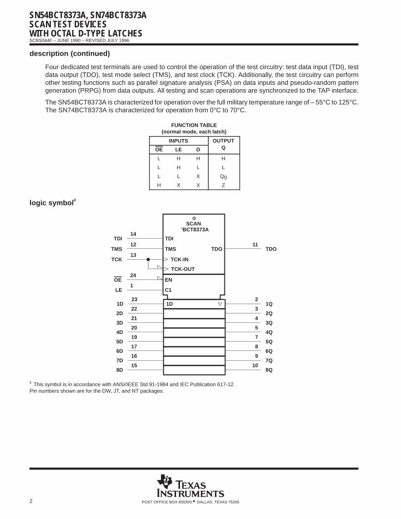
FUNCTION TABLE(normal mode, each latch)
INPUTS OUTPUT
OE LE D Q
L H H H
L H L L
L L X Q0
H X X Z
logic symbol †
SCAN’BCT8373A
1D23
1D 1Q2
TDI14
TDI
TCK-IN
EN24
222D 2Q
3
TMS12
TMS13
TCK
C11
LE
TCK-OUT
213D 3Q
4
204D 4Q
5
195D 5Q
7
176D 6Q
8
167D 7Q
9
158D 8Q
10
OE
Φ
TDO11
TDO
† This symbol is in accordance with ANSI/IEEE Std 91-1984 and IEC Publication 617-12.Pin numbers shown are for the DW, JT, and NT packages.
SN54BCT8373A, SN74BCT8373ASCAN TEST DEVICES
WITH OCTAL D-TYPE LATCHES
SCBS044F – JUNE 1990 – REVISED JULY 1996
3POST OFFICE BOX 655303 • DALLAS, TEXAS 75265
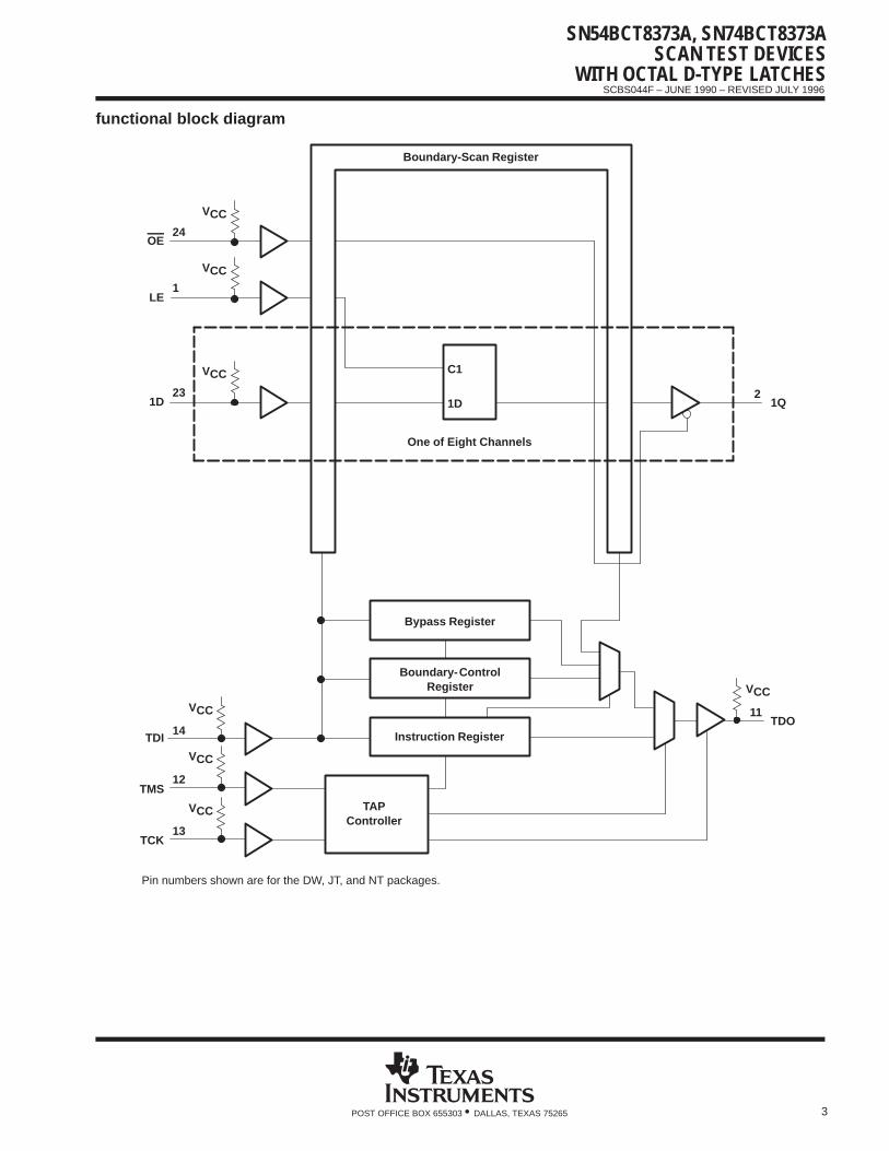
functional block diagram
Boundary-ControlRegister
Bypass Register
Boundary-Scan Register
Instruction RegisterTDI
TMS
TCK
TDO
TAPController
VCC
VCC
OE
VCC
VCC
VCC
LE
1D
VCC
VCC
One of Eight Channels
1Q
C1
1D
24
1
23
14
12
13
2
11
Pin numbers shown are for the DW, JT, and NT packages.

SN54BCT8373A, SN74BCT8373ASCAN TEST DEVICESWITH OCTAL D-TYPE LATCHES
SCBS044F – JUNE 1990 – REVISED JULY 1996
4 POST OFFICE BOX 655303 • DALLAS, TEXAS 75265
Terminal Functions
TERMINALNAME DESCRIPTION
1D–8DNormal-function data inputs. See function table for normal-mode logic. Internal pullups force these inputs to a high level ifleft unconnected.
GND Ground
LENormal-function latch-enable input. See function table for normal-mode logic. An internal pullup forces LE to a high level ifleft unconnected.
OENormal-function output-enable input. See function table for normal-mode logic. An internal pullup forces OE to a high levelif left unconnected.
1Q–8Q Normal-function data outputs. See function table for normal-mode logic.
TCKTest clock. One of four terminals required by IEEE Standard 1149.1-1990. Test operations of the device are synchronous toTCK. Data is captured on the rising edge of TCK and outputs change on the falling edge of TCK. An internal pullup forcesTCK to a high level if left unconnected.
TDITest data input. One of four terminals required by IEEE Standard 1149.1-1990. TDI is the serial input for shifting data throughthe instruction register or selected data register. An internal pullup forces TDI to a high level if left unconnected.
TDOTest data output. One of four terminals required by IEEE Standard 1149.1-1990. TDO is the serial output for shifting datathrough the instruction register or selected data register. An internal pullup forces TDO to a high level when it is not activeand is not driven from an external source.
TMS
Test mode select. One of four terminals required by IEEE Standard 1149.1-1990. TMS directs the device through its TAPcontroller states. An internal pullup forces TMS to a high level if left unconnected. The TMS pin also provides the optionaltest reset signal of IEEE Standard 1149.1-1990. This is implemented by recognizing a third logic level, double-high (VIHH),at TMS.
VCC Supply voltage
SN54BCT8373A, SN74BCT8373ASCAN TEST DEVICES
WITH OCTAL D-TYPE LATCHES
SCBS044F – JUNE 1990 – REVISED JULY 1996
5POST OFFICE BOX 655303 • DALLAS, TEXAS 75265
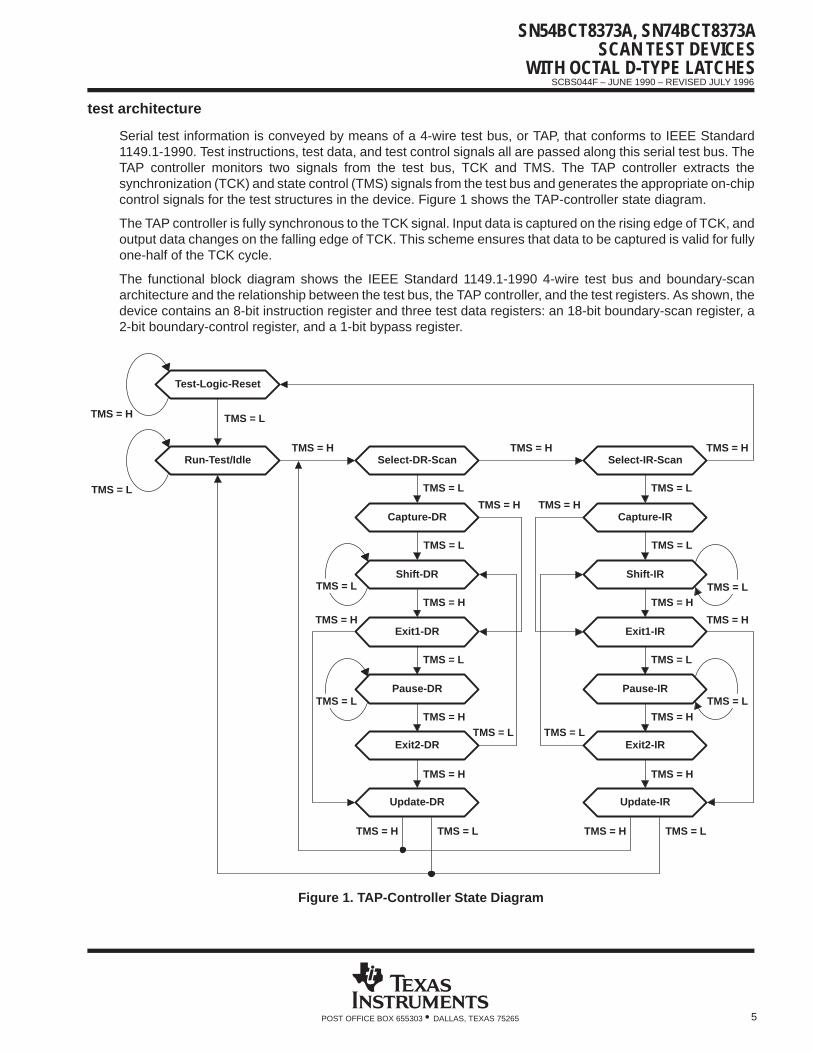
test architecture
Serial test information is conveyed by means of a 4-wire test bus, or TAP, that conforms to IEEE Standard1149.1-1990. Test instructions, test data, and test control signals all are passed along this serial test bus. TheTAP controller monitors two signals from the test bus, TCK and TMS. The TAP controller extracts thesynchronization (TCK) and state control (TMS) signals from the test bus and generates the appropriate on-chipcontrol signals for the test structures in the device. Figure 1 shows the TAP-controller state diagram.
The TAP controller is fully synchronous to the TCK signal. Input data is captured on the rising edge of TCK, andoutput data changes on the falling edge of TCK. This scheme ensures that data to be captured is valid for fullyone-half of the TCK cycle.
The functional block diagram shows the IEEE Standard 1149.1-1990 4-wire test bus and boundary-scanarchitecture and the relationship between the test bus, the TAP controller, and the test registers. As shown, thedevice contains an 8-bit instruction register and three test data registers: an 18-bit boundary-scan register, a2-bit boundary-control register, and a 1-bit bypass register.
Test-Logic-Reset
Run-Test/Idle Select-DR-Scan
Capture-DR
Shift-DR
Exit1-DR
Pause-DR
Update-DR
TMS = L
TMS = L
TMS = H
TMS = L
TMS = H
TMS = H
TMS = LTMS = H
TMS = L
TMS = L
TMS = H
TMS = LExit2-DR
Select-IR-Scan
Capture-IR
Shift-IR
Exit1-IR
Pause-IR
Update-IR
TMS = L
TMS = L
TMS = H
TMS = L
TMS = H
TMS = H
TMS = LTMS = H
TMS = LExit2-IR
TMS = L
TMS = H TMS = H
TMS = H
TMS = L
TMS = H
TMS = L
TMS = HTMS = H
TMS = H
TMS = L
Figure 1. TAP-Controller State Diagram
SN54BCT8373A, SN74BCT8373ASCAN TEST DEVICESWITH OCTAL D-TYPE LATCHES
SCBS044F – JUNE 1990 – REVISED JULY 1996
6 POST OFFICE BOX 655303 • DALLAS, TEXAS 75265
state diagram description
The TAP controller is a synchronous finite state machine that provides test control signals throughout the device.The state diagram shown in Figure 1 is in accordance with IEEE Standard 1149.1-1990. The TAP controllerproceeds through its states based on the level of TMS at the rising edge of TCK.
As shown, the TAP controller consists of 16 states. There are six stable states (indicated by a looping arrow inthe state diagram) and ten unstable states. A stable state is a state the TAP controller can retain for consecutiveTCK cycles. Any state that does not meet this criterion is an unstable state.
There are two main paths though the state diagram: one to access and control the selected data register andone to access and control the instruction register. Only one register can be accessed at a time.
Test-Logic-Reset
The device powers up in the Test-Logic-Reset state. In the stable Test-Logic-Reset state, the test logic is resetand is disabled so that the normal logic function of the device is performed. The instruction register is reset toan opcode that selects the optional IDCODE instruction, if supported, or the BYPASS instruction. Certain dataregisters also can be reset to their power-up values.
The state machine is constructed such that the TAP controller returns to the Test-Logic-Reset state in no morethan five TCK cycles if TMS is left high. The TMS pin has an internal pullup resistor that forces it high if leftunconnected or if a board defect causes is to be open circuited.
For the ′BCT8373A, the instruction register is reset to the binary value 11111111, which selects the BYPASSinstruction. The boundary-control register is reset to the binary value 10, which selects the PSA test operation.
Run-Test / Idle
The TAP controller must pass through the Run-Test/Idle state (from Test-Logic-Reset) before executing any testoperations. The Run-Test/Idle state also can be entered, following data-register or instruction-register scans.Run-Test/Idle is a stable state in which the test logic may be actively running a test or may be idle.
The test operations selected by the boundary-control register are performed while the TAP controller is in theRun-Test/Idle state.
Select-DR-Scan, Select-lR-Scan
No specific function is performed in the Select-DR-Scan and Select-lR-Scan states, and the TAP controller exitseither of these states on the next TCK cycle. These states allow the selection of either data-register scan orinstruction-register scan.
Capture-DR
When a data-register scan is selected, the TAP controller must pass through the Capture-DR state. In theCapture-DR state, the selected data register may capture a data value, as specified by the current instruction.Such capture operations occur on the rising edge of TCK, upon which the TAP controller exits the Capture-DRstate.
Shift-DR
Upon entry to the Shift-DR state, the data register is placed in the scan path between TDI and TDO and, on thefirst falling edge of TCK, TDO goes from the high-impedance state to an active state. TDO enables to the logiclevel present in the least-significant bit of the selected data register.
While in the stable Shift-DR state, data is serially shifted through the selected data register on each TCK cycle.The first shift occurs on the first rising edge of TCK after entry to the Shift-DR state (i.e., no shifting occurs duringthe TCK cycle, in which the TAP controller changes from Capture-DR to Shift-DR or from Exit2-DR to Shift-DR).The last shift occurs on the rising edge of TCK, upon which the TAP controller exits the Shift-DR state.
SN54BCT8373A, SN74BCT8373ASCAN TEST DEVICES
WITH OCTAL D-TYPE LATCHES
SCBS044F – JUNE 1990 – REVISED JULY 1996
7POST OFFICE BOX 655303 • DALLAS, TEXAS 75265
Exit1-DR, Exit2-DR
The Exit1-DR and Exit2-DR states are temporary states that end a data register scan. It is possible to returnto the Shift-DR state from either Exit1-DR or Exit2-DR without recapturing the data register.
On the first falling edge of TCK after entry to Exit1-DR, TDO goes from the active state to the high-impedancestate.
Pause-DR
No specific function is performed in the stable Pause-DR state, in which the TAP controller can remainindefinitely. The Pause-DR state suspends and resumes data-register scan operations without loss of data.
Update-DR
If the current instruction calls for the selected data register to be updated with current data, then such updateoccurs on the falling edge of TCK, following entry to the Update-DR state.
Capture-IR
When an instruction-register scan is selected, the TAP controller must pass through the Capture-IR state. Inthe Capture-IR state, the instruction register captures its current status value. This capture operation occurson the rising edge of TCK, upon which the TAP controller exits the Capture-IR state.
For the ′BCT8373A, the status value loaded in the Capture-IR state is the fixed binary value 10000001.
Shift-IR
Upon entry to the Shift-IR state, the instruction register is placed in the scan path between TDI and TDO and,on the first falling edge of TCK, TDO goes from the high-impedance state to an active state. TDO enables tothe logic level present in the least-significant bit of the instruction register.
While in the stable Shift-IR state, instruction data is serially shifted through the instruction register on each TCKcycle. The first shift occurs on the first rising edge of TCK after entry to the Shift-IR state (i.e., no shifting occursduring the TCK cycle, in which the TAP controller changes from Capture-IR to Shift-IR or from Exit2-IR toShift-IR). The last shift occurs on the rising edge of TCK, upon which the TAP controller exits the Shift-IR state.
Exit1-IR, Exit2-IR
The Exit1-IR and Exit2-IR states are temporary states used to end an instruction-register scan. It is possibleto return to the Shift-IR state from either Exit1-IR or Exit2-IR without recapturing the instruction register.
On the first falling edge of TCK after entry to Exit1-IR, TDO goes from the active state to the high-impedancestate.
Pause-IR
No specific function is performed in the stable Pause-IR state, in which the TAP controller can remainindefinitely. The Pause-IR state suspends and resumes instruction-register scan operations without loss ofdata.
Update-IR
The current instruction is updated and takes effect on the falling edge of TCK, following entry to the Update-IRstate.
SN54BCT8373A, SN74BCT8373ASCAN TEST DEVICESWITH OCTAL D-TYPE LATCHES
SCBS044F – JUNE 1990 – REVISED JULY 1996
8 POST OFFICE BOX 655303 • DALLAS, TEXAS 75265
register overview
With the exception of the bypass register, any test register may be thought of as a serial shift register with ashadow latch on each bit. The bypass register differs in that it contains only a shift register. During theappropriate capture state (Capture-IR for instruction register, Capture-DR for data registers), the shift registermay be parallel loaded from a source specified by the current instruction. During the appropriate shift state(Shift-IR or Shift-DR), the contents of the shift register are shifted out from TDO while new contents are shiftedin at TDI. During the appropriate update state (Update-IR or Update-DR), the shadow latches are updated fromthe shift register.
instruction register description
The instruction register (IR) is eight bits long and tells the device what instruction is to be executed. Informationcontained in the instruction includes the mode of operation (either normal mode, in which the device performsits normal logic function, or test mode, in which the normal logic function is inhibited or altered), the test operationto be performed, which of the three data registers is to be selected for inclusion in the scan path duringdata-register scans, and the source of data to be captured into the selected data register during Capture-DR.
Table 2 lists the instructions supported by the ′BCT8373A. The even-parity feature specified for SCOPEdevices is not supported in this device. Bit 7 of the instruction opcode is a don’t-care bit. Any instructions thatare defined for SCOPE devices but are not supported by this device default to BYPASS.
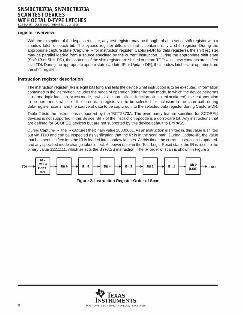
During Capture-IR, the IR captures the binary value 10000001. As an instruction is shifted in, this value is shiftedout via TDO and can be inspected as verification that the IR is in the scan path. During Update-IR, the valuethat has been shifted into the IR is loaded into shadow latches. At this time, the current instruction is updated,and any specified mode change takes effect. At power up or in the Test-Logic-Reset state, the IR is reset to thebinary value 11111111, which selects the BYPASS instruction. The IR order of scan is shown in Figure 2.
Bit 6 Bit 5 Bit 4 Bit 3 Bit 2 Bit 1 TDOTDI
Bit 7(MSB)Don’tCare
Bit 0(LSB)
Figure 2. Instruction Register Order of Scan
SN54BCT8373A, SN74BCT8373ASCAN TEST DEVICES
WITH OCTAL D-TYPE LATCHES
SCBS044F – JUNE 1990 – REVISED JULY 1996
9POST OFFICE BOX 655303 • DALLAS, TEXAS 75265
data register description
boundary-scan register
The boundary-scan register (BSR) is 18 bits long. It contains one boundary-scan cell (BSC) for eachnormal-function input pin and one BSC for each normal-function output pin. The BSR is used 1) to store testdata that is to be applied internally to the inputs of the normal on-chip logic and/or externally to the device outputpins, and/or 2) to capture data that appears internally at the outputs of the normal on-chip logic and/or externallyat the device input pins.
The source of data to be captured into the BSR during Capture-DR is determined by the current instruction. Thecontents of the BSR may change during Run-Test/Idle as determined by the current instruction. The contentsof the BSR are not changed in Test-Logic-Reset.
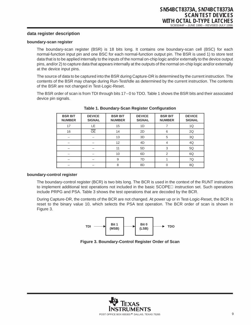
The BSR order of scan is from TDI through bits 17–0 to TDO. Table 1 shows the BSR bits and their associateddevice pin signals.
Table 1. Boundary-Scan Register Configuration
BSR BITNUMBER
DEVICE SIGNAL
BSR BITNUMBER
DEVICE SIGNAL
BSR BITNUMBER
DEVICE SIGNAL
17 LE 15 1D 7 1Q
16 OE 14 2D 6 2Q
– – 13 3D 5 3Q
– – 12 4D 4 4Q
– – 11 5D 3 5Q
– – 10 6D 2 6Q
– – 9 7D 1 7Q
– – 8 8D 0 8Q
boundary-control register
The boundary-control register (BCR) is two bits long. The BCR is used in the context of the RUNT instructionto implement additional test operations not included in the basic SCOPE instruction set. Such operationsinclude PRPG and PSA. Table 3 shows the test operations that are decoded by the BCR.
During Capture-DR, the contents of the BCR are not changed. At power up or in Test-Logic-Reset, the BCR isreset to the binary value 10, which selects the PSA test operation. The BCR order of scan is shown inFigure 3.
TDOTDIBit 0(LSB)
Bit 1(MSB)
Figure 3. Boundary-Control Register Order of Scan
SN54BCT8373A, SN74BCT8373ASCAN TEST DEVICESWITH OCTAL D-TYPE LATCHES
SCBS044F – JUNE 1990 – REVISED JULY 1996
10 POST OFFICE BOX 655303 • DALLAS, TEXAS 75265
bypass register
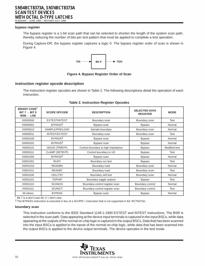
The bypass register is a 1-bit scan path that can be selected to shorten the length of the system scan path,thereby reducing the number of bits per test pattern that must be applied to complete a test operation.
During Capture-DR, the bypass register captures a logic 0. The bypass register order of scan is shown inFigure 4.
Bit 0 TDOTDI
Figure 4. Bypass Register Order of Scan
instruction register opcode description
The instruction register opcodes are shown in Table 2. The following descriptions detail the operation of eachinstruction.
Table 2. Instruction Register Opcodes
BINARY CODE†
BIT 7 → BIT 0MSB → LSB
SCOPE OPCODE DESCRIPTIONSELECTED DATA
REGISTER MODE
X0000000 EXTEST/INTEST Boundary scan Boundary scan Test
X0000001 BYPASS‡ Bypass scan Bypass Normal
X0000010 SAMPLE/PRELOAD Sample boundary Boundary scan Normal
X0000011 INTEST/EXTEST Boundary scan Boundary scan Test
X0000100 BYPASS‡ Bypass scan Bypass Normal
X0000101 BYPASS‡ Bypass scan Bypass Normal
X0000110 HIGHZ (TRIBYP) Control boundary to high impedance Bypass Modified test
X0000111 CLAMP (SETBYP) Control boundary to 1/0 Bypass Test
X0001000 BYPASS‡ Bypass scan Bypass Normal
X0001001 RUNT Boundary run test Bypass Test
X0001010 READBN Boundary read Boundary scan Normal
X0001011 READBT Boundary read Boundary scan Test
X0001100 CELLTST Boundary self test Boundary scan Normal
X0001101 TOPHIP Boundary toggle outputs Bypass Test
X0001110 SCANCN Boundary-control register scan Boundary control Normal
X0001111 SCANCT Boundary-control register scan Boundary control Test
All others BYPASS Bypass scan Bypass Normal
† Bit 7 is a don’t-care bit; X = don’t care.‡ The BYPASS instruction is executed in lieu of a SCOPE instruction that is not supported in the ′BCT8373A.
boundary scan
This instruction conforms to the IEEE Standard 1149.1-1990 EXTEST and INTEST instructions. The BSR isselected in the scan path. Data appearing at the device input terminals is captured in the input BSCs, while dataappearing at the outputs of the normal on-chip logic is captured in the output BSCs. Data that has been scannedinto the input BSCs is applied to the inputs of the normal on-chip logic, while data that has been scanned intothe output BSCs is applied to the device output terminals. The device operates in the test mode.
SN54BCT8373A, SN74BCT8373ASCAN TEST DEVICES
WITH OCTAL D-TYPE LATCHES
SCBS044F – JUNE 1990 – REVISED JULY 1996
11POST OFFICE BOX 655303 • DALLAS, TEXAS 75265
bypass scan
This instruction conforms to the IEEE Standard 1149.1-1990 BYPASS instruction. The bypass register isselected in the scan path. A logic 0 value is captured in the bypass register during Capture-DR. The deviceoperates in the normal mode.
sample boundary
This instruction conforms to the IEEE Standard 1149.1-1990 SAMPLE/PRELOAD instruction. The BSR isselected in the scan path. Data appearing at the device input terminals is captured in the input BSCs, while dataappearing at the outputs of the normal on-chip logic is captured in the output BSCs. The device operates in thenormal mode.
control boundary to high impedance
This instruction conforms to the IEEE Standard 1149.1a-1993 HIGHZ instruction. The bypass register isselected in the scan path. A logic 0 value is captured in the bypass register during Capture-DR. The deviceoperates in a modified test mode in which all device output terminals are placed in the high-impedance state,the device input terminals remain operational, and the normal on-chip logic function is performed.
control boundary to 1/0
This instruction conforms to the IEEE Standard 1149.1a-1993 CLAMP instruction. The bypass register isselected in the scan path. A logic 0 value is captured in the bypass register during Capture-DR. Data in the inputBSCs is applied to the inputs of the normal on-chip logic, while data in the output BSCs is applied to the deviceoutput terminals. The device operates in the test mode.
boundary run test
The bypass register is selected in the scan path. A logic 0 value is captured in the bypass register duringCapture-DR. The device operates in the test mode. The test operation specified in the BCR is executed duringRun-Test/Idle. The four test operations decoded by the BCR are: sample inputs/toggle outputs (TOPSIP),PRPG, PSA, and simultaneous PSA and PRPG (PSA/PRPG).
boundary read
The BSR is selected in the scan path. The value in the BSR remains unchanged during Capture-DR. Thisinstruction is useful for inspecting data after a PSA operation.
boundary self test
The BSR is selected in the scan path. All BSCs capture the inverse of their current values during Capture-DR.In this way, the contents of the shadow latches may be read out to verify the integrity of both shift-register andshadow-latch elements of the BSR. The device operates in the normal mode.
boundary toggle outputs
The bypass register is selected in the scan path. A logic 0 value is captured in the bypass register duringCapture-DR. Data in the shift register elements of the selected output BSCs is toggled on each rising edge ofTCK in Run-Test/Idle and is then updated in the shadow latches and applied to the associated device outputterminals on each falling edge of TCK in Run-Test/Idle. Data in the selected input BSCs remains constant andis applied to the inputs of the normal on-chip logic. Data appearing at the device input terminals is not capturedin the input BSCs. The device operates in the test mode.
boundary-control register scan
The BCR is selected in the scan path. The value in the BCR remains unchanged during Capture-DR. Thisoperation must be performed before a boundary run test operation in order to specify which test operation isto be executed.
SN54BCT8373A, SN74BCT8373ASCAN TEST DEVICESWITH OCTAL D-TYPE LATCHES
SCBS044F – JUNE 1990 – REVISED JULY 1996
12 POST OFFICE BOX 655303 • DALLAS, TEXAS 75265
boundary-control register opcode description
The BCR opcodes are decoded from BCR bits 1–0 as shown in Table 3. The selected test operation isperformed while the RUNT instruction is executed in the Run-Test/Idle state. The following descriptions detailthe operation of each BCR instruction and illustrate the associated PSA and PRPG algorithms.
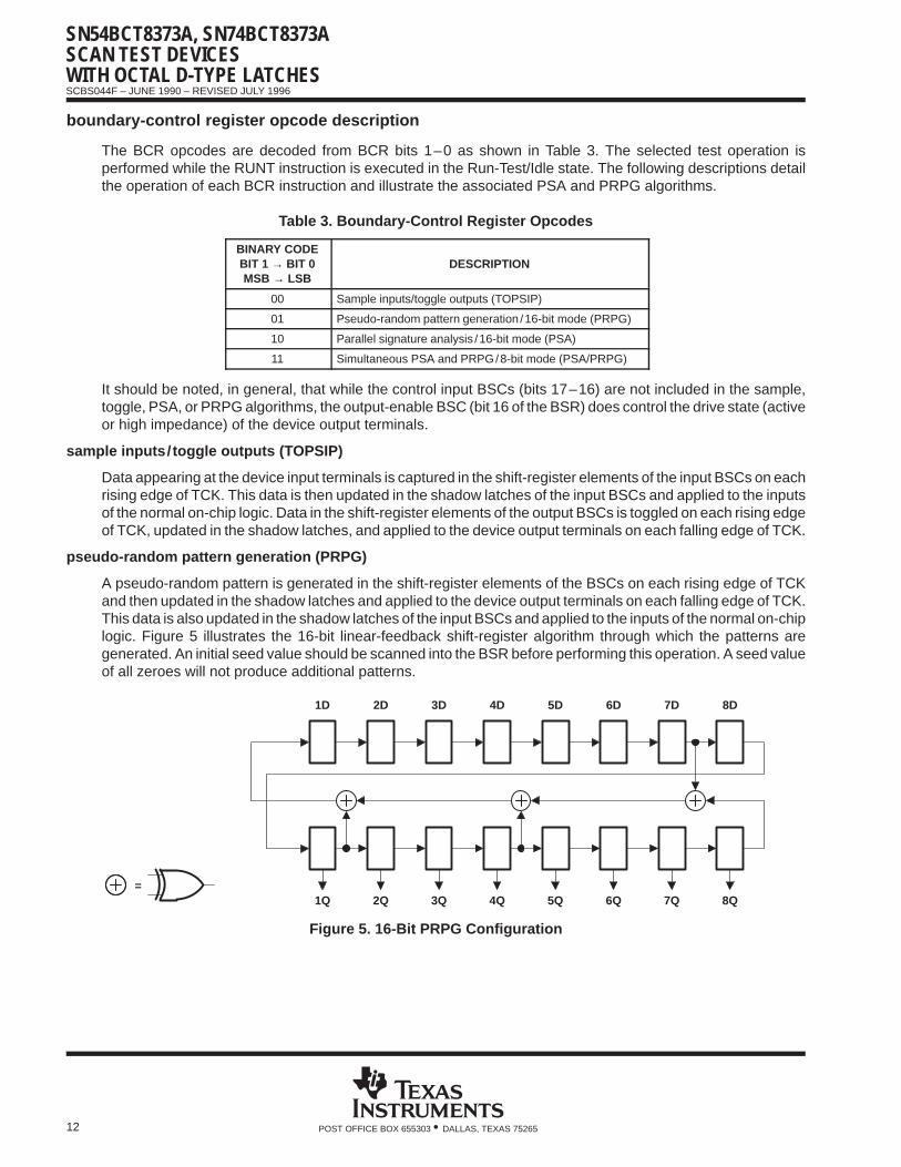
Table 3. Boundary-Control Register Opcodes
BINARY CODEBIT 1 → BIT 0MSB → LSB
DESCRIPTION
00 Sample inputs/toggle outputs (TOPSIP)
01 Pseudo-random pattern generation /16-bit mode (PRPG)
10 Parallel signature analysis /16-bit mode (PSA)
11 Simultaneous PSA and PRPG/8-bit mode (PSA/PRPG)
It should be noted, in general, that while the control input BSCs (bits 17–16) are not included in the sample,toggle, PSA, or PRPG algorithms, the output-enable BSC (bit 16 of the BSR) does control the drive state (activeor high impedance) of the device output terminals.
sample inputs/ toggle outputs (TOPSIP)
Data appearing at the device input terminals is captured in the shift-register elements of the input BSCs on eachrising edge of TCK. This data is then updated in the shadow latches of the input BSCs and applied to the inputsof the normal on-chip logic. Data in the shift-register elements of the output BSCs is toggled on each rising edgeof TCK, updated in the shadow latches, and applied to the device output terminals on each falling edge of TCK.
pseudo-random pattern generation (PRPG)
A pseudo-random pattern is generated in the shift-register elements of the BSCs on each rising edge of TCKand then updated in the shadow latches and applied to the device output terminals on each falling edge of TCK.This data is also updated in the shadow latches of the input BSCs and applied to the inputs of the normal on-chiplogic. Figure 5 illustrates the 16-bit linear-feedback shift-register algorithm through which the patterns aregenerated. An initial seed value should be scanned into the BSR before performing this operation. A seed valueof all zeroes will not produce additional patterns.
=
1D
1Q
2D 3D 4D 5D 6D 7D 8D
2Q 3Q 4Q 5Q 6Q 7Q 8Q
Figure 5. 16-Bit PRPG Configuration
SN54BCT8373A, SN74BCT8373ASCAN TEST DEVICES
WITH OCTAL D-TYPE LATCHES
SCBS044F – JUNE 1990 – REVISED JULY 1996
13POST OFFICE BOX 655303 • DALLAS, TEXAS 75265
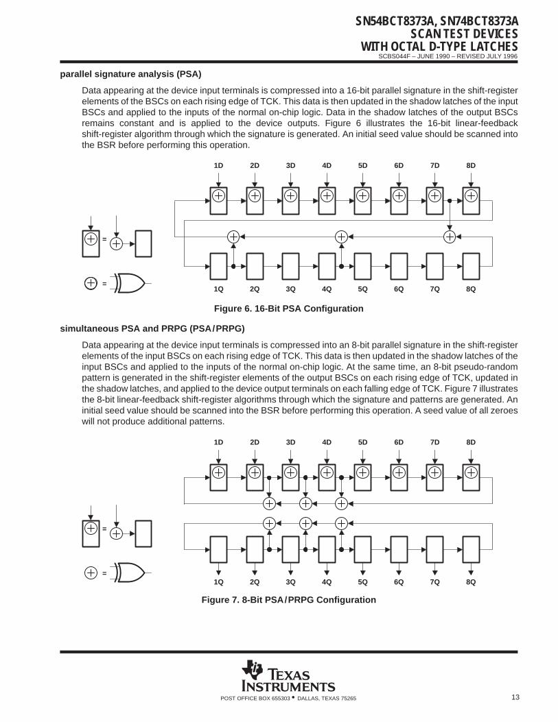
parallel signature analysis (PSA)
Data appearing at the device input terminals is compressed into a 16-bit parallel signature in the shift-registerelements of the BSCs on each rising edge of TCK. This data is then updated in the shadow latches of the inputBSCs and applied to the inputs of the normal on-chip logic. Data in the shadow latches of the output BSCsremains constant and is applied to the device outputs. Figure 6 illustrates the 16-bit linear-feedbackshift-register algorithm through which the signature is generated. An initial seed value should be scanned intothe BSR before performing this operation.
=
1D
1Q
2D 3D 4D 5D 6D 7D 8D
2Q 3Q 4Q 5Q 6Q 7Q 8Q
=
Figure 6. 16-Bit PSA Configuration
simultaneous PSA and PRPG (PSA/PRPG)
Data appearing at the device input terminals is compressed into an 8-bit parallel signature in the shift-registerelements of the input BSCs on each rising edge of TCK. This data is then updated in the shadow latches of theinput BSCs and applied to the inputs of the normal on-chip logic. At the same time, an 8-bit pseudo-randompattern is generated in the shift-register elements of the output BSCs on each rising edge of TCK, updated inthe shadow latches, and applied to the device output terminals on each falling edge of TCK. Figure 7 illustratesthe 8-bit linear-feedback shift-register algorithms through which the signature and patterns are generated. Aninitial seed value should be scanned into the BSR before performing this operation. A seed value of all zeroeswill not produce additional patterns.
=
1D
1Q
2D 3D 4D 5D 6D 7D 8D
2Q 3Q 4Q 5Q 6Q 7Q 8Q
=
Figure 7. 8-Bit PSA/PRPG Configuration
SN54BCT8373A, SN74BCT8373ASCAN TEST DEVICESWITH OCTAL D-TYPE LATCHES
SCBS044F – JUNE 1990 – REVISED JULY 1996
14 POST OFFICE BOX 655303 • DALLAS, TEXAS 75265
timing description
All test operations of the ′BCT8373A are synchronous to the test clock (TCK). Data on the TDI, TMS, andnormal-function inputs is captured on the rising edge of TCK. Data appears on the TDO and normal-functionoutput terminals on the falling edge of TCK. The TAP controller is advanced through its states (as shown inFigure 1) by changing the value of TMS on the falling edge of TCK and then applying a rising edge to TCK.
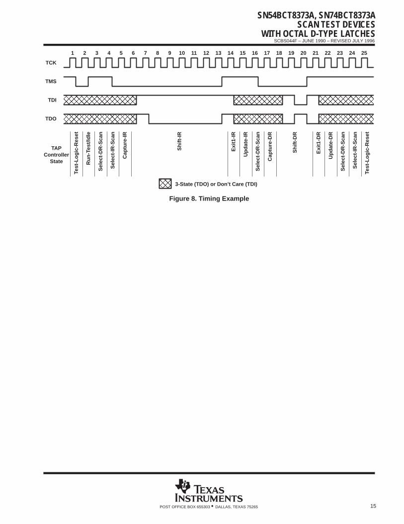
A simple timing example is shown in Figure 8. In this example, the TAP controller begins in the Test-Logic-Resetstate and is advanced through its states, as necessary, to perform one instruction-register scan and onedata-register scan. While in the Shift-IR and Shift-DR states, TDI is used to input serial data and TDO is usedto output serial data. The TAP controller is then returned to the Test-Logic-Reset state. Table 4 details theoperation of the test circuitry during each TCK cycle.
Table 4. Explanation of Timing Example
TCKCYCLE(S)
TAP STATEAFTER TCK DESCRIPTION
1 Test-Logic-ResetTMS is changed to a logic 0 value on the falling edge of TCK to begin advancing the TAP controller towardthe desired state.
2 Run-Test/Idle
3 Select-DR-Scan
4 Select-IR-Scan
5 Capture-IRThe IR captures the 8-bit binary value 10000001 on the rising edge of TCK as the TAP controller exits theCapture-IR state.
6 Shift-IRTDO becomes active and TDI is made valid on the falling edge of TCK. The first bit is shifted into the TAP onthe rising edge of TCK as the TAP controller advances to the next state.
7–13 Shift-IR
One bit is shifted into the IR on each TCK rising edge. With TDI held at a logic 1 value, the 8-bit binary value11111111 is serially scanned into the IR. At the same time, the 8-bit binary value 10000001 is serially scannedout of the IR via TDO. In TCK cycle 13, TMS is changed to a logic 1 value to end the IR scan on the next TCKcycle. The last bit of the instruction is shifted as the TAP controller advances from Shift-IR to Exit1-IR.
14 Exit1-IR TDO becomes inactive (goes to the high-impedance state) on the falling edge of TCK.
15 Update-IR The IR is updated with the new instruction (BYPASS) on the falling edge of TCK.
16 Select-DR-Scan
17 Capture-DRThe bypass register captures a logic 0 value on the rising edge of TCK as the TAP controller exits theCapture-DR state.
18 Shift-DRTDO becomes active, and TDI is made valid, on the falling edge of TCK. The first bit is shifted into the TAPon the rising edge of TCK as the TAP controller advances to the next state.
19–20 Shift-DR The binary value 101 is shifted in via TDI, while the binary value 010 is shifted out via TDO.
21 Exit1-DR TDO becomes inactive (goes to the high-impedance state) on the falling edge of TCK.
22 Update-DR In general, the selected data register is updated with the new data on the falling edge of TCK.
23 Select-DR-Scan
24 Select-IR-Scan
25 Test-Logic-Reset Test operation completed
SN54BCT8373A, SN74BCT8373ASCAN TEST DEVICES
WITH OCTAL D-TYPE LATCHES
SCBS044F – JUNE 1990 – REVISED JULY 1996
15POST OFFICE BOX 655303 • DALLAS, TEXAS 75265
ÎÎÎÎÎÎÎÎÎÎÎÎ
ÎÎÎÎÎÎÎÎÎÎ
ÎÎÎÎÎÎÎÎÎÎÎÎÎÎÎÎ
ÎÎÎÎÎÎÎÎÎÎÎÎÎÎÎÎ
1 2 3 4 5 6 7 8 9 10 11 12 13 14 15 16 17 18 19 20 21 22 23 24 25
ÎÎÎÎÎÎÎÎÎÎ
ÎÎÎÎÎÎÎÎÎÎÎÎ
Test
-Log
ic-R
eset
Run
-Tes
t/Idl
e
Sel
ect-
DR
-Sca
n
Sel
ect-
IR-S
can
Cap
ture
-IR
Shi
ft-IR
Exi
t1-I
R
Upd
ate-
IR
Sel
ect-
DR
-Sca
n
Cap
ture
-DR
Shi
ft-D
R
Exi
t1-D
R
Upd
ate-
DR
Sel
ect-
DR
-Sca
n
Sel
ect-
IR-S
can
Test
-Log
ic-R
eset
TCK
TMS
TDI
TDO
ÎÎÎÎ
TAPController
State
3-State (TDO) or Don’t Care (TDI)
Figure 8. Timing Example
SN54BCT8373A, SN74BCT8373ASCAN TEST DEVICESWITH OCTAL D-TYPE LATCHES
SCBS044F – JUNE 1990 – REVISED JULY 1996
16 POST OFFICE BOX 655303 • DALLAS, TEXAS 75265
absolute maximum ratings over operating free-air temperature range (unless otherwise noted) †
Supply voltage range, VCC –0.5 V to 7 V. . . . . . . . . . . . . . . . . . . . . . . . . . . . . . . . . . . . . . . . . . . . . . . . . . . . . . . . . . Input voltage range, VI: Except TMS (see Note 1) –0.5 V to 7 V. . . . . . . . . . . . . . . . . . . . . . . . . . . . . . . . . . . . . .
TMS (see Note 1) –0.5 V to 12 V. . . . . . . . . . . . . . . . . . . . . . . . . . . . . . . . . . . . . . . . . . . Voltage range applied to any output in the disabled or power-off state –0.5 V to 5.5 V. . . . . . . . . . . . . . . . . . . . Voltage range applied to any output in the high state –0.5 V to VCC. . . . . . . . . . . . . . . . . . . . . . . . . . . . . . . . . . Input clamp current –30 mA. . . . . . . . . . . . . . . . . . . . . . . . . . . . . . . . . . . . . . . . . . . . . . . . . . . . . . . . . . . . . . . . . . . . . Current into any output in the low state: SN54BCT8373A (TDO) 40 mA. . . . . . . . . . . . . . . . . . . . . . . . . . . . . . .
SN54BCT8373A (Any Q) 96 mA. . . . . . . . . . . . . . . . . . . . . . . . . . . . . SN74BCT8373A (TDO) 48 mA. . . . . . . . . . . . . . . . . . . . . . . . . . . . . . . SN74BCT8373A (Any Q) 128 mA. . . . . . . . . . . . . . . . . . . . . . . . . . . .
Maximum power dissipation at TA = 55°C (in still air) (see Note 2): DW package 1.7 W. . . . . . . . . . . . . . . . . . NT package 1.3 W. . . . . . . . . . . . . . . . . . .
Storage temperature range, Tstg –65°C to 150°C. . . . . . . . . . . . . . . . . . . . . . . . . . . . . . . . . . . . . . . . . . . . . . . . . . .
† Stresses beyond those listed under “absolute maximum ratings” may cause permanent damage to the device. These are stress ratings only andfunctional operation of the device at these or any other conditions beyond those indicated under “recommended operating conditions” is notimplied. Exposure to absolute-maximum-rated conditions for extended periods may affect device reliability.
NOTES: 1. The input voltage rating may be exceeded if the input clamp-current rating is observed.2. The maximum package power dissipation is calculated using a junction temperature of 150°C and a board trace length of 750 mils,
except for the NT package, which has a trace length of zero. For more information, refer to the Package Thermal Considerationsapplication note in the ABT Advanced BiCMOS Technology Data Book, literature number SCBD002.
recommended operating conditions
SN54BCT8373A SN74BCT8373AUNIT
MIN NOM MAX MIN NOM MAXUNIT
VCC Supply voltage 4.5 5 5.5 4.5 5 5.5 V
VIH High-level input voltage 2 2 V
VIHH Double-high-level input voltage TMS 10 12 10 12 V
VIL Low-level input voltage 0.8 0.8 V
IIK Input clamp current –18 –18 mA
IOH High level output currentTDO –3 –3
mAIOH High-level output currentAny Q –12 –15
mA
IOL Low level output currentTDO 20 24
mAIOL Low-level output currentAny Q 48 64
mA
TA Operating free-air temperature –55 125 0 70 °C
SN54BCT8373A, SN74BCT8373ASCAN TEST DEVICES
WITH OCTAL D-TYPE LATCHES
SCBS044F – JUNE 1990 – REVISED JULY 1996
17POST OFFICE BOX 655303 • DALLAS, TEXAS 75265
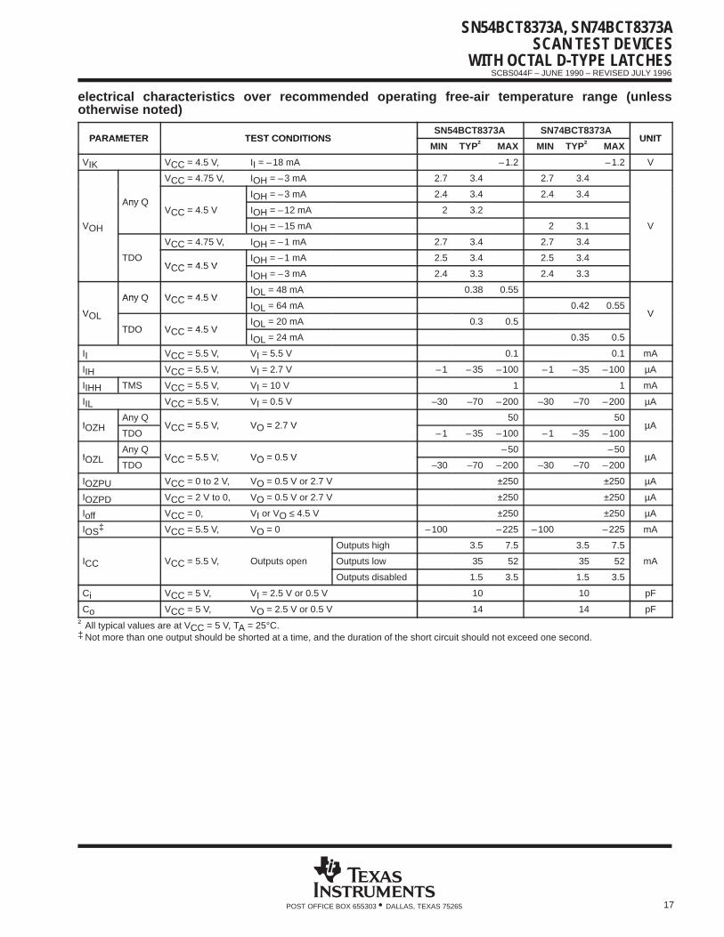
electrical characteristics over recommended operating free-air temperature range (unlessotherwise noted)
PARAMETER TEST CONDITIONSSN54BCT8373A SN74BCT8373A
UNITPARAMETER TEST CONDITIONSMIN TYP† MAX MIN TYP† MAX
UNIT
VIK VCC = 4.5 V, II = –18 mA –1.2 –1.2 V
VCC = 4.75 V, IOH = –3 mA 2.7 3.4 2.7 3.4
Any QIOH = –3 mA 2.4 3.4 2.4 3.4
Any QVCC = 4.5 V IOH = –12 mA 2 3.2
VOH IOH = –15 mA 2 3.1 V
VCC = 4.75 V, IOH = –1 mA 2.7 3.4 2.7 3.4
TDOVCC = 4 5 V
IOH = –1 mA 2.5 3.4 2.5 3.4VCC = 4.5 V
IOH = –3 mA 2.4 3.3 2.4 3.3
Any Q VCC = 4 5 VIOL = 48 mA 0.38 0.55
VOL
Any Q VCC = 4.5 VIOL = 64 mA 0.42 0.55
VVOLTDO VCC = 4 5 V
IOL = 20 mA 0.3 0.5V
TDO VCC = 4.5 VIOL = 24 mA 0.35 0.5
II VCC = 5.5 V, VI = 5.5 V 0.1 0.1 mA
IIH VCC = 5.5 V, VI = 2.7 V –1 –35 –100 –1 –35 –100 µA
IIHH TMS VCC = 5.5 V, VI = 10 V 1 1 mA
IIL VCC = 5.5 V, VI = 0.5 V –30 –70 –200 –30 –70 –200 µA
IOZHAny Q
VCC = 5 5 V VO = 2 7 V50 50
µAIOZHTDO
VCC = 5.5 V, VO = 2.7 V–1 –35 –100 –1 –35 –100
µA
IOZLAny Q
VCC = 5 5 V VO = 0 5 V–50 –50
µAIOZLTDO
VCC = 5.5 V, VO = 0.5 V–30 –70 –200 –30 –70 –200
µA
IOZPU VCC = 0 to 2 V, VO = 0.5 V or 2.7 V ±250 ±250 µA
IOZPD VCC = 2 V to 0, VO = 0.5 V or 2.7 V ±250 ±250 µA
Ioff VCC = 0, VI or VO ≤ 4.5 V ±250 ±250 µA
IOS‡ VCC = 5.5 V, VO = 0 –100 –225 –100 –225 mA
Outputs high 3.5 7.5 3.5 7.5
ICC VCC = 5.5 V, Outputs open Outputs low 35 52 35 52 mA
Outputs disabled 1.5 3.5 1.5 3.5
Ci VCC = 5 V, VI = 2.5 V or 0.5 V 10 10 pF
Co VCC = 5 V, VO = 2.5 V or 0.5 V 14 14 pF
† All typical values are at VCC = 5 V, TA = 25°C.‡ Not more than one output should be shorted at a time, and the duration of the short circuit should not exceed one second.
SN54BCT8373A, SN74BCT8373ASCAN TEST DEVICESWITH OCTAL D-TYPE LATCHES
SCBS044F – JUNE 1990 – REVISED JULY 1996
18 POST OFFICE BOX 655303 • DALLAS, TEXAS 75265
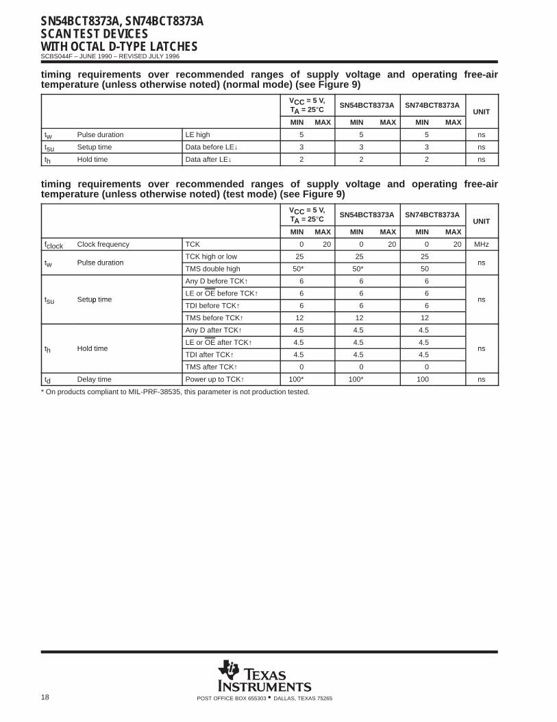
timing requirements over recommended ranges of supply voltage and operating free-airtemperature (unless otherwise noted) (normal mode) (see Figure 9)
VCC = 5 V,TA = 25°C SN54BCT8373A SN74BCT8373A
UNITMIN MAX MIN MAX MIN MAX
tw Pulse duration LE high 5 5 5 ns
tsu Setup time Data before LE↓ 3 3 3 ns
th Hold time Data after LE↓ 2 2 2 ns
timing requirements over recommended ranges of supply voltage and operating free-airtemperature (unless otherwise noted) (test mode) (see Figure 9)
VCC = 5 V,TA = 25°C SN54BCT8373A SN74BCT8373A
UNITMIN MAX MIN MAX MIN MAX
fclock Clock frequency TCK 0 20 0 20 0 20 MHz
t Pulse durationTCK high or low 25 25 25
nstw Pulse durationTMS double high 50* 50* 50
ns
Any D before TCK↑ 6 6 6
t Setup timeLE or OE before TCK↑ 6 6 6
nstsu Setup timeTDI before TCK↑ 6 6 6
ns
TMS before TCK↑ 12 12 12
Any D after TCK↑ 4.5 4.5 4.5
th Hold timeLE or OE after TCK↑ 4.5 4.5 4.5
nsth Hold timeTDI after TCK↑ 4.5 4.5 4.5
ns
TMS after TCK↑ 0 0 0
td Delay time Power up to TCK↑ 100* 100* 100 ns
* On products compliant to MIL-PRF-38535, this parameter is not production tested.
SN54BCT8373A, SN74BCT8373ASCAN TEST DEVICES
WITH OCTAL D-TYPE LATCHES
SCBS044F – JUNE 1990 – REVISED JULY 1996
19POST OFFICE BOX 655303 • DALLAS, TEXAS 75265
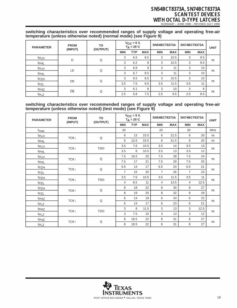
switching characteristics over recommended ranges of supply voltage and operating free-airtemperature (unless otherwise noted) (normal mode) (see Figure 9)
PARAMETERFROM
(INPUT)TO
(OUTPUT)
VCC = 5 V,TA = 25°C SN54BCT8373A SN74BCT8373A
UNIT(INPUT) (OUTPUT)MIN TYP MAX MIN MAX MIN MAX
tPLHD Q
3 6.5 8.5 3 10.5 3 9.5ns
tPHLD Q
3 6.2 8 3 10.5 3 9.5ns
tPLHLE Q
3 6.8 9 3 11 3 10ns
tPHLLE Q
3 6.7 8.5 3 11 3 10ns
tPZHOE Q
3 6.5 8.5 3 10.5 3 10ns
tPZLOE Q
3.5 7.5 9.5 3.5 11.5 3.5 11ns
tPHZ OE Q3 6.1 8 3 10 3 9
nstPLZ
OE Q2.5 5.8 7.5 2.5 9.5 2.5 8.5
ns
switching characteristics over recommended ranges of supply voltage and operating free-airtemperature (unless otherwise noted) (test mode) (see Figure 9)
PARAMETERFROM
(INPUT)TO
(OUTPUT)
VCC = 5 V,TA = 25°C SN54BCT8373A SN74BCT8373A
UNIT(INPUT) (OUTPUT)MIN TYP MAX MIN MAX MIN MAX
fmax 20 20 20 MHz
tPLHTCK↓ Q
6 13 15.5 6 21.5 6 20 ns
tPHLTCK↓ Q
6 12.5 15.5 6 21.5 6 20 ns
tPLHTCK↓ TDO
3.5 7.6 10.5 3.5 14 3.5 13ns
tPHLTCK↓ TDO
3.5 8 10.5 3.5 13 3.5 12ns
tPLHTCK↑ Q
7.5 16.5 20 7.5 28 7.5 24ns
tPHLTCK↑ Q
7.5 17 21 7.5 29 7.5 25ns
tPZHTCK↓ Q
6.5 14 17 6.5 24 6.5 21ns
tPZLTCK↓ Q
7 15 20 7 26 7 23ns
tPZHTCK↓ TDO
3.5 7.6 10.5 3.5 11.5 3.5 11ns
tPZLTCK↓ TDO
4 8.5 11 4 13.5 4 12.5ns
tPZHTCK↑ Q
8 18 22 8 30 8 27ns
tPZLTCK↑ Q
8 19 25 8 32 8 29ns
tPHZTCK↓ Q
6 14 18 6 24 6 22ns
tPLZTCK↓ Q
6 14 17 6 23 6 21ns
tPHZTCK↓ TDO
3 8 11.5 3 13 3 12.5ns
tPLZTCK↓ TDO
3 7.5 10 3 13 3 12ns
tPHZTCK↑ Q
8 18.5 22 8 31 8 27ns
tPLZTCK↑ Q
8 18.5 22 8 31 8 27ns
SN54BCT8373A, SN74BCT8373ASCAN TEST DEVICESWITH OCTAL D-TYPE LATCHES
SCBS044F – JUNE 1990 – REVISED JULY 1996
20 POST OFFICE BOX 655303 • DALLAS, TEXAS 75265
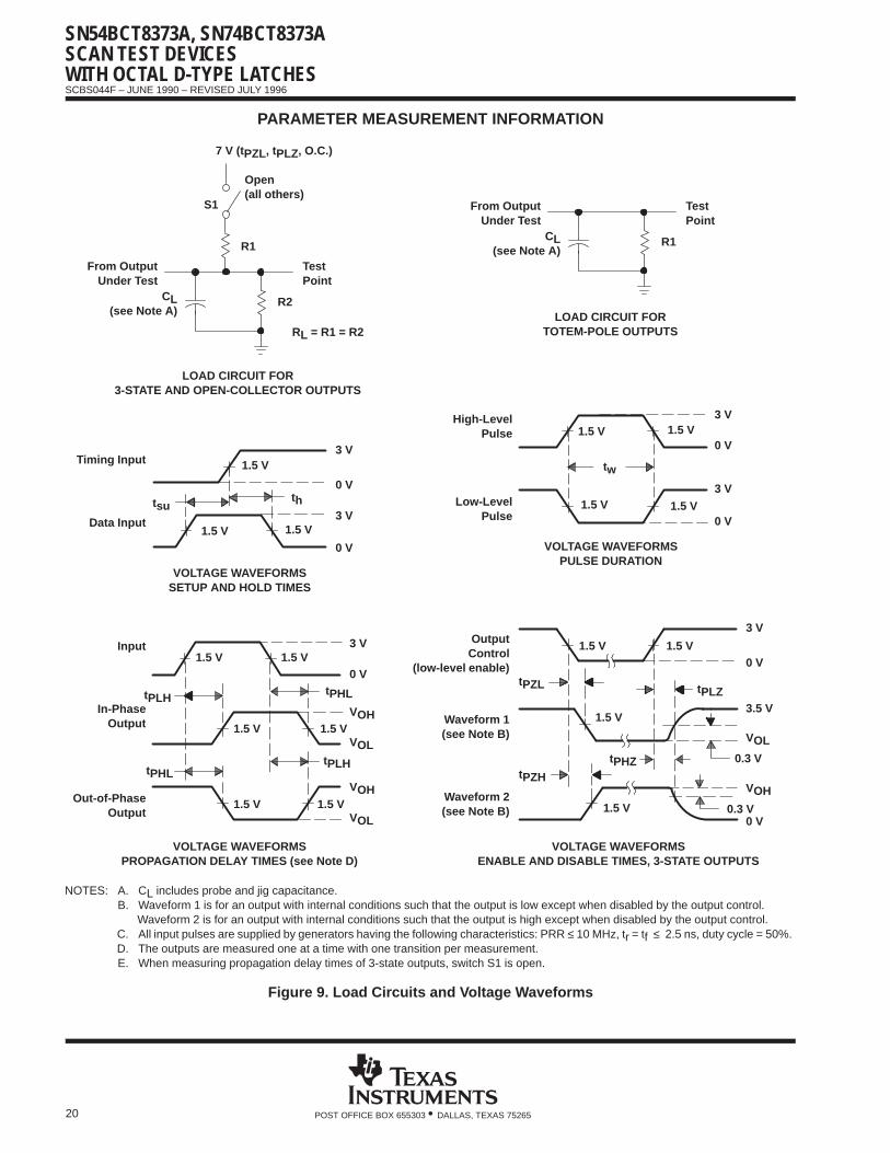
PARAMETER MEASUREMENT INFORMATION
From OutputUnder Test
TestPoint
R1CL(see Note A)
LOAD CIRCUIT FORTOTEM-POLE OUTPUTS
LOAD CIRCUIT FOR3-STATE AND OPEN-COLLECTOR OUTPUTS
R1
S1
7 V (tPZL, tPLZ, O.C.)
Open(all others)
From OutputUnder Test
TestPoint
R2CL(see Note A)
RL = R1 = R2
1.5 V
1.5 V1.5 V
3 V
3 V
0 V
0 V
thtsu
VOLTAGE WAVEFORMSSETUP AND HOLD TIMES
Timing Input
Data Input
1.5 V 1.5 V3 V
3 V
0 V
0 V
High-LevelPulse
Low-LevelPulse
tw
VOLTAGE WAVEFORMSPULSE DURATION
1.5 V 1.5 V
tPHLtPLH
tPLHtPHL
Input
Out-of-PhaseOutput
1.5 V 1.5 V
1.5 V1.5 V
1.5 V 1.5 V
3 V
0 V
VOL
VOH
VOH
VOL
In-PhaseOutput
VOLTAGE WAVEFORMSPROPAGATION DELAY TIMES (see Note D)
tPHZ
tPLZ
0.3 V
tPZL
tPZH
1.5 V1.5 V
1.5 V
1.5 V
3 V
0 V
OutputControl
(low-level enable)
Waveform 1(see Note B)
Waveform 2(see Note B)
0 V
VOH
VOL
3.5 V
0.3 V
VOLTAGE WAVEFORMSENABLE AND DISABLE TIMES, 3-STATE OUTPUTS
NOTES: A. CL includes probe and jig capacitance.B. Waveform 1 is for an output with internal conditions such that the output is low except when disabled by the output control.
Waveform 2 is for an output with internal conditions such that the output is high except when disabled by the output control.C. All input pulses are supplied by generators having the following characteristics: PRR ≤ 10 MHz, tr = tf ≤ 2.5 ns, duty cycle = 50%.D. The outputs are measured one at a time with one transition per measurement.E. When measuring propagation delay times of 3-state outputs, switch S1 is open.
Figure 9. Load Circuits and Voltage Waveforms
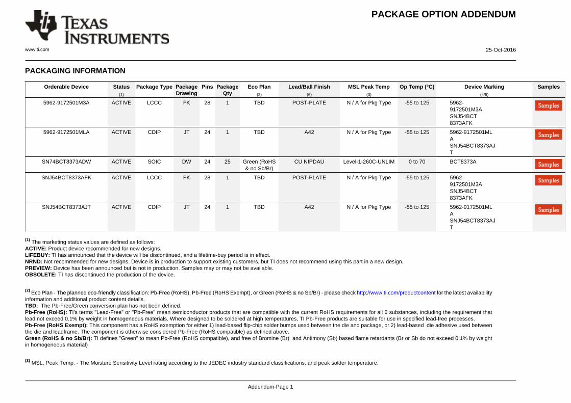
PACKAGE OPTION ADDENDUM
www.ti.com 25-Oct-2016
Addendum-Page 1
PACKAGING INFORMATION
Orderable Device Status(1)
Package Type PackageDrawing
Pins PackageQty
Eco Plan(2)
Lead/Ball Finish(6)
MSL Peak Temp(3)
Op Temp (°C) Device Marking(4/5)
Samples
5962-9172501M3A ACTIVE LCCC FK 28 1 TBD POST-PLATE N / A for Pkg Type -55 to 125 5962-9172501M3ASNJ54BCT8373AFK
5962-9172501MLA ACTIVE CDIP JT 24 1 TBD A42 N / A for Pkg Type -55 to 125 5962-9172501MLASNJ54BCT8373AJT
SN74BCT8373ADW ACTIVE SOIC DW 24 25 Green (RoHS& no Sb/Br)
CU NIPDAU Level-1-260C-UNLIM 0 to 70 BCT8373A
SNJ54BCT8373AFK ACTIVE LCCC FK 28 1 TBD POST-PLATE N / A for Pkg Type -55 to 125 5962-9172501M3ASNJ54BCT8373AFK
SNJ54BCT8373AJT ACTIVE CDIP JT 24 1 TBD A42 N / A for Pkg Type -55 to 125 5962-9172501MLASNJ54BCT8373AJT
(1) The marketing status values are defined as follows:ACTIVE: Product device recommended for new designs.LIFEBUY: TI has announced that the device will be discontinued, and a lifetime-buy period is in effect.NRND: Not recommended for new designs. Device is in production to support existing customers, but TI does not recommend using this part in a new design.PREVIEW: Device has been announced but is not in production. Samples may or may not be available.OBSOLETE: TI has discontinued the production of the device.
(2) Eco Plan - The planned eco-friendly classification: Pb-Free (RoHS), Pb-Free (RoHS Exempt), or Green (RoHS & no Sb/Br) - please check http://www.ti.com/productcontent for the latest availabilityinformation and additional product content details.TBD: The Pb-Free/Green conversion plan has not been defined.Pb-Free (RoHS): TI's terms "Lead-Free" or "Pb-Free" mean semiconductor products that are compatible with the current RoHS requirements for all 6 substances, including the requirement thatlead not exceed 0.1% by weight in homogeneous materials. Where designed to be soldered at high temperatures, TI Pb-Free products are suitable for use in specified lead-free processes.Pb-Free (RoHS Exempt): This component has a RoHS exemption for either 1) lead-based flip-chip solder bumps used between the die and package, or 2) lead-based die adhesive used betweenthe die and leadframe. The component is otherwise considered Pb-Free (RoHS compatible) as defined above.Green (RoHS & no Sb/Br): TI defines "Green" to mean Pb-Free (RoHS compatible), and free of Bromine (Br) and Antimony (Sb) based flame retardants (Br or Sb do not exceed 0.1% by weightin homogeneous material)
(3) MSL, Peak Temp. - The Moisture Sensitivity Level rating according to the JEDEC industry standard classifications, and peak solder temperature.

PACKAGE OPTION ADDENDUM
www.ti.com 25-Oct-2016
Addendum-Page 2
(4) There may be additional marking, which relates to the logo, the lot trace code information, or the environmental category on the device.
(5) Multiple Device Markings will be inside parentheses. Only one Device Marking contained in parentheses and separated by a "~" will appear on a device. If a line is indented then it is a continuationof the previous line and the two combined represent the entire Device Marking for that device.
(6) Lead/Ball Finish - Orderable Devices may have multiple material finish options. Finish options are separated by a vertical ruled line. Lead/Ball Finish values may wrap to two lines if the finishvalue exceeds the maximum column width.
Important Information and Disclaimer:The information provided on this page represents TI's knowledge and belief as of the date that it is provided. TI bases its knowledge and belief on informationprovided by third parties, and makes no representation or warranty as to the accuracy of such information. Efforts are underway to better integrate information from third parties. TI has taken andcontinues to take reasonable steps to provide representative and accurate information but may not have conducted destructive testing or chemical analysis on incoming materials and chemicals.TI and TI suppliers consider certain information to be proprietary, and thus CAS numbers and other limited information may not be available for release.
In no event shall TI's liability arising out of such information exceed the total purchase price of the TI part(s) at issue in this document sold by TI to Customer on an annual basis.
OTHER QUALIFIED VERSIONS OF SN54BCT8373A, SN74BCT8373A :
• Catalog: SN74BCT8373A
• Military: SN54BCT8373A
NOTE: Qualified Version Definitions:
• Catalog - TI's standard catalog product
• Military - QML certified for Military and Defense Applications
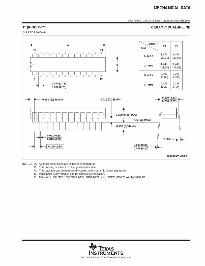
MECHANICAL DATA
MCER004A – JANUARY 1995 – REVISED JANUARY 1997
POST OFFICE BOX 655303 • DALLAS, TEXAS 75265
JT (R-GDIP-T**) CERAMIC DUAL-IN-LINE24 LEADS SHOWN
4040110/C 08/96
B
0.200 (5,08) MAX
0.320 (8,13)0.290 (7,37)
0.130 (3,30) MIN
0.008 (0,20)0.014 (0,36)
Seating Plane
13
12
0.030 (0,76)0.070 (1,78)
0.015 (0,38) MIN
A
24
1
0.100 (2,54) MAX
0.023 (0,58)0.015 (0,38)
0.100 (2,54)
0°–15°
1.440
(37,08) 1.460
0.285
(7,39) 0.291
(36,58)
(7,24)
28PINS **
1.280
1.240
0.300
0.245
(7,62)
DIM
B MAX
A MAX
A MIN
B MIN(6,22)
24
(32,51)
(31,50)
NOTES: A. All linear dimensions are in inches (millimeters).B. This drawing is subject to change without notice.C. This package can be hermetically sealed with a ceramic lid using glass frit.D. Index point is provided on cap for terminal identification.E. Falls within MIL STD 1835 GDIP3-T24, GDIP4-T28, and JEDEC MO-058 AA, MO-058 AB

IMPORTANT NOTICE
Texas Instruments Incorporated (TI) reserves the right to make corrections, enhancements, improvements and other changes to itssemiconductor products and services per JESD46, latest issue, and to discontinue any product or service per JESD48, latest issue. Buyersshould obtain the latest relevant information before placing orders and should verify that such information is current and complete.TI’s published terms of sale for semiconductor products (http://www.ti.com/sc/docs/stdterms.htm) apply to the sale of packaged integratedcircuit products that TI has qualified and released to market. Additional terms may apply to the use or sale of other types of TI products andservices.Reproduction of significant portions of TI information in TI data sheets is permissible only if reproduction is without alteration and isaccompanied by all associated warranties, conditions, limitations, and notices. TI is not responsible or liable for such reproduceddocumentation. Information of third parties may be subject to additional restrictions. Resale of TI products or services with statementsdifferent from or beyond the parameters stated by TI for that product or service voids all express and any implied warranties for theassociated TI product or service and is an unfair and deceptive business practice. TI is not responsible or liable for any such statements.Buyers and others who are developing systems that incorporate TI products (collectively, “Designers”) understand and agree that Designersremain responsible for using their independent analysis, evaluation and judgment in designing their applications and that Designers havefull and exclusive responsibility to assure the safety of Designers' applications and compliance of their applications (and of all TI productsused in or for Designers’ applications) with all applicable regulations, laws and other applicable requirements. Designer represents that, withrespect to their applications, Designer has all the necessary expertise to create and implement safeguards that (1) anticipate dangerousconsequences of failures, (2) monitor failures and their consequences, and (3) lessen the likelihood of failures that might cause harm andtake appropriate actions. Designer agrees that prior to using or distributing any applications that include TI products, Designer willthoroughly test such applications and the functionality of such TI products as used in such applications.TI’s provision of technical, application or other design advice, quality characterization, reliability data or other services or information,including, but not limited to, reference designs and materials relating to evaluation modules, (collectively, “TI Resources”) are intended toassist designers who are developing applications that incorporate TI products; by downloading, accessing or using TI Resources in anyway, Designer (individually or, if Designer is acting on behalf of a company, Designer’s company) agrees to use any particular TI Resourcesolely for this purpose and subject to the terms of this Notice.TI’s provision of TI Resources does not expand or otherwise alter TI’s applicable published warranties or warranty disclaimers for TIproducts, and no additional obligations or liabilities arise from TI providing such TI Resources. TI reserves the right to make corrections,enhancements, improvements and other changes to its TI Resources. TI has not conducted any testing other than that specificallydescribed in the published documentation for a particular TI Resource.Designer is authorized to use, copy and modify any individual TI Resource only in connection with the development of applications thatinclude the TI product(s) identified in such TI Resource. NO OTHER LICENSE, EXPRESS OR IMPLIED, BY ESTOPPEL OR OTHERWISETO ANY OTHER TI INTELLECTUAL PROPERTY RIGHT, AND NO LICENSE TO ANY TECHNOLOGY OR INTELLECTUAL PROPERTYRIGHT OF TI OR ANY THIRD PARTY IS GRANTED HEREIN, including but not limited to any patent right, copyright, mask work right, orother intellectual property right relating to any combination, machine, or process in which TI products or services are used. Informationregarding or referencing third-party products or services does not constitute a license to use such products or services, or a warranty orendorsement thereof. Use of TI Resources may require a license from a third party under the patents or other intellectual property of thethird party, or a license from TI under the patents or other intellectual property of TI.TI RESOURCES ARE PROVIDED “AS IS” AND WITH ALL FAULTS. TI DISCLAIMS ALL OTHER WARRANTIES ORREPRESENTATIONS, EXPRESS OR IMPLIED, REGARDING RESOURCES OR USE THEREOF, INCLUDING BUT NOT LIMITED TOACCURACY OR COMPLETENESS, TITLE, ANY EPIDEMIC FAILURE WARRANTY AND ANY IMPLIED WARRANTIES OFMERCHANTABILITY, FITNESS FOR A PARTICULAR PURPOSE, AND NON-INFRINGEMENT OF ANY THIRD PARTY INTELLECTUALPROPERTY RIGHTS. TI SHALL NOT BE LIABLE FOR AND SHALL NOT DEFEND OR INDEMNIFY DESIGNER AGAINST ANY CLAIM,INCLUDING BUT NOT LIMITED TO ANY INFRINGEMENT CLAIM THAT RELATES TO OR IS BASED ON ANY COMBINATION OFPRODUCTS EVEN IF DESCRIBED IN TI RESOURCES OR OTHERWISE. IN NO EVENT SHALL TI BE LIABLE FOR ANY ACTUAL,DIRECT, SPECIAL, COLLATERAL, INDIRECT, PUNITIVE, INCIDENTAL, CONSEQUENTIAL OR EXEMPLARY DAMAGES INCONNECTION WITH OR ARISING OUT OF TI RESOURCES OR USE THEREOF, AND REGARDLESS OF WHETHER TI HAS BEENADVISED OF THE POSSIBILITY OF SUCH DAMAGES.Unless TI has explicitly designated an individual product as meeting the requirements of a particular industry standard (e.g., ISO/TS 16949and ISO 26262), TI is not responsible for any failure to meet such industry standard requirements.Where TI specifically promotes products as facilitating functional safety or as compliant with industry functional safety standards, suchproducts are intended to help enable customers to design and create their own applications that meet applicable functional safety standardsand requirements. Using products in an application does not by itself establish any safety features in the application. Designers mustensure compliance with safety-related requirements and standards applicable to their applications. Designer may not use any TI products inlife-critical medical equipment unless authorized officers of the parties have executed a special contract specifically governing such use.Life-critical medical equipment is medical equipment where failure of such equipment would cause serious bodily injury or death (e.g., lifesupport, pacemakers, defibrillators, heart pumps, neurostimulators, and implantables). Such equipment includes, without limitation, allmedical devices identified by the U.S. Food and Drug Administration as Class III devices and equivalent classifications outside the U.S.TI may expressly designate certain products as completing a particular qualification (e.g., Q100, Military Grade, or Enhanced Product).Designers agree that it has the necessary expertise to select the product with the appropriate qualification designation for their applicationsand that proper product selection is at Designers’ own risk. Designers are solely responsible for compliance with all legal and regulatoryrequirements in connection with such selection.Designer will fully indemnify TI and its representatives against any damages, costs, losses, and/or liabilities arising out of Designer’s non-compliance with the terms and provisions of this Notice.
Mailing Address: Texas Instruments, Post Office Box 655303, Dallas, Texas 75265Copyright © 2017, Texas Instruments Incorporated