samsung emmc product family · datasheet emmc rev. 1.21 klm8g1getf-b041 samsung confidential...
TRANSCRIPT

- 1 -
SAMSUNG ELECTRONICS RESERVES THE RIGHT TO CHANGE PRODUCTS, INFORMATION AND SPECIFICATIONS WITHOUT NOTICE.
Products and specifications discussed herein are for reference purposes only. All information discussed herein is provided on an "AS IS" basis, without warranties of any kind.
This document and all information discussed herein remain the sole and exclusive property of Samsung Electronics. No license of any patent, copyright, mask work, trademark or any other intellectual property right is granted by one party to the other party under this document, by implication, estoppel or other-wise.
Samsung products are not intended for use in life support, critical care, medical, safety equipment, or similar applications where product failure could result in loss of life or personal or physical harm, or any military or defense application, or any governmental procurement to which special terms or provisions may apply.
For updates or additional information about Samsung products, contact your nearest Samsung office.
All brand names, trademarks and registered trademarks belong to their respective owners.
2017 Samsung Electronics Co., Ltd. All rights reserved
Rev. 1.21 Jul. 2017
SAMSUNG CONFIDENTIAL
KLM8G1GETF-B041KLMAG1JETD-B041KLMBG2JETD-B041KLMCG4JETD-B041
Samsung eMMC Product familyeMMC 5.1 Specification compatibility
datasheet

- 2 -
IF THERE IS ANY OTHER OPERATION TO IMPLEMENT IN ADDITION TO SPECIFICATIONIN THE DATASHEET OR JEDEC STANDARD, PLEASE CONTACT EACH BRANCH OFFICE OR HEADQUARTERS OF SAMSUNG ELECTRONICS.
datasheet eMMCRev. 1.21
SAMSUNG CONFIDENTIALKLM8G1GETF-B041KLMAG1JETD-B041KLMBG2JETD-B041KLMCG4JETD-B041
Revision History
Revision No. History Draft Date Remark Editor
0.0 1. Initial issue Aug. 22, 2016 Target S.M.Lee
1.0 1. Customer sample Nov. 15,2016 Final S.M.Lee
1.1 1. 8GB is added (Customer sample) Dec. 12,2016 Final S.M.Lee
1.2 1. Typo correction Jan. 26, 2017 Final S.M.Lee
1.21 1. Typo correction Jul. 10, 2017 Final S.M.Lee

- 3 -
IF THERE IS ANY OTHER OPERATION TO IMPLEMENT IN ADDITION TO SPECIFICATIONIN THE DATASHEET OR JEDEC STANDARD, PLEASE CONTACT EACH BRANCH OFFICE OR HEADQUARTERS OF SAMSUNG ELECTRONICS.
Table Of Contents
datasheet eMMCRev. 1.21
SAMSUNG CONFIDENTIALKLM8G1GETF-B041KLMAG1JETD-B041KLMBG2JETD-B041KLMCG4JETD-B041
1.0 PRODUCT LIST..........................................................................................................................................................4
2.0 KEY FEATURES......................................................................................................................................................... 4
3.0 PACKAGE CONFIGURATIONS ................................................................................................................................. 53.1 153 Ball Pin Configuration ....................................................................................................................................... 5
3.1.1 11.5mm x 13mm x 0.8mm Package Dimension [8GB /16GB] .......................................................................... 63.1.2 11.5mm x 13mm x 0.8mm Package Dimension [32GB] ................................................................................... 63.1.3 11.5mm x 13mm x 1.0mm Package Dimension [64GB] ................................................................................... 7
3.2 Product Architecture ................................................................................................................................................ 8
4.0 HS400 mode...............................................................................................................................................................9
5.0 New eMMC5.1 Features ............................................................................................................................................. 105.1 Overview.................................................................................................................................................................. 105.2 Command Queuing ................................................................................................................................................. 10
5.2.1 CMD Set Description......................................................................................................................................... 105.2.2 New Response : QSR (Queue Status Register) .............................................................................................. 105.2.3 Send Status : CMD13 ...................................................................................................................................... 105.2.4 Mechanism of CMD Queue operation............................................................................................................... 115.2.5 CMD Queue Register description ..................................................................................................................... 11
5.3 Enhanced Strobe Mode........................................................................................................................................... 115.4 RPMB Throughput improve ..................................................................................................................................... 115.5 Secure Write Protection........................................................................................................................................... 12
6.0 Technical Notes ..........................................................................................................................................................136.1 S/W Algorithm.......................................................................................................................................................... 13
6.1.1 Partition Management ....................................................................................................................................... 136.1.1.1 Enhanced Partition (Area) .......................................................................................................................... 13
6.1.2 Boot operation................................................................................................................................................... 136.1.3 User Density...................................................................................................................................................... 146.1.4 Auto Power Saving Mode.................................................................................................................................. 156.1.5 Performance...................................................................................................................................................... 15
7.0 REGISTER VALUE..................................................................................................................................................... 167.1 OCR Register .......................................................................................................................................................... 167.2 CID Register ............................................................................................................................................................ 16
7.2.1 Product name table (In CID Register) ............................................................................................................... 167.3 CSD Register........................................................................................................................................................... 177.4 Extended CSD Register .......................................................................................................................................... 18
8.0 AC PARAMETER........................................................................................................................................................ 238.1 Timing Parameter .................................................................................................................................................... 238.2 Previous Bus Timing Parameters for DDR52 and HS200 mode are defined by JEDEC standard.......................... 238.3 Bus Timing Specification in HS400 mode ............................................................................................................... 24
8.3.1 HS400 Device Input Timing .............................................................................................................................. 248.3.2 HS400 Device Output Timing............................................................................................................................ 25
8.4 Bus signal levels...................................................................................................................................................... 268.4.1 Open-drain mode bus signal level..................................................................................................................... 268.4.2 Push-pull mode bus signal level eMMC ............................................................................................................ 26
9.0 DC PARAMETER .......................................................................................................................................................279.1 Active Power Consumption during operation .......................................................................................................... 279.2 Standby Power Consumption in auto power saving mode and standby state......................................................... 279.3 Sleep Power Consumption in Sleep State............................................................................................................... 279.4 Supply Voltage ........................................................................................................................................................ 279.5 Bus Signal Line Load............................................................................................................................................... 28

- 4 -
IF THERE IS ANY OTHER OPERATION TO IMPLEMENT IN ADDITION TO SPECIFICATIONIN THE DATASHEET OR JEDEC STANDARD, PLEASE CONTACT EACH BRANCH OFFICE OR HEADQUARTERS OF SAMSUNG ELECTRONICS.
datasheet eMMCRev. 1.21
SAMSUNG CONFIDENTIALKLM8G1GETF-B041KLMAG1JETD-B041KLMBG2JETD-B041KLMCG4JETD-B041
INTRODUCTION
SAMSUNG eMMC is an embedded MMC solution designed in a BGA package form. eMMC operation is identical to a MMC device and therefore is a sim-ple read and write to memory using MMC protocol v5.1 which is a industry standard.
eMMC consists of NAND flash and a MMC controller. 3V supply voltage is required for the NAND area (VDDF or VCC) whereas 1.8V or 3V dual supply
voltage (VDD or VCCQ) is supported for the MMC controller. SAMSUNG eMMC supports HS400 in order to improve sequential bandwidth, especially
sequential read performance.
There are several advantages of using eMMC. It is easy to use as the MMC interface allows easy integration with any microprocessor with MMC host. Any revision or amendment of NAND is invisible to the host as the embedded MMC controller insulates NAND technology from the host. This leads to faster product development as well as faster times to market.
The embedded flash management software or FTL(Flash Transition Layer) of eMMC manages Wear Leveling, Bad Block Management and ECC. The FTL supports all features of the Samsung NAND flash and achieves optimal performance.
1.0 PRODUCT LIST[Table 1] Product List
2.0 KEY FEATURES
embedded MultiMediaCard Ver. 5.1 compatible.
SAMSUNG eMMC supports features of eMMC5.1 which are defined in JEDEC Standard
- Major Supported Features : HS400, Field Firmware Update, Cache, Command Queuing, Enhanced Strobe Mode, Secure Write Protection, Partition types. - Non-supported Features : Large Sector Size (4KB) Backward compatibility with previous MultiMediaCard system specification (1bit data bus, multi-eMMC systems)
Data bus width : 1bit (Default), 4bit and 8bit
MMC I/F Clock Frequency : 0 ~ 200MHz MMC I/F Boot Frequency : 0 ~ 52MHz
Temperature : Operation (-25C ~ 85C), Storage without operation (-40C ~ 85C)
Power : Interface power → VCCQ(1.70V ~ 1.95V) , Memory power → VCC (2.7V ~ 3.6V)
Capacities eMMC Part ID NAND Flash Type User Density (%) Power System Package size Pin Configuration
8 GB KLM8G1GETF-B041 64Gb x 1
91.0%
- Interface power : VDD (1.70V ~ 1.95V or
2.7V ~ 3.6V) - Memory power :
VDDF (2.7V ~ 3.6V)
11.5mm x 13mm x 0.8mm153FBGA
16 GB KLMAG1JETD-B041 128Gb x 1
32 GB KLMBG2JETD-B041 128Gb x 2
64 GB KLMCG4JETD-B041 128Gb x 4 11.5mm x 13mm x 1.0mm

- 5 -
IF THERE IS ANY OTHER OPERATION TO IMPLEMENT IN ADDITION TO SPECIFICATIONIN THE DATASHEET OR JEDEC STANDARD, PLEASE CONTACT EACH BRANCH OFFICE OR HEADQUARTERS OF SAMSUNG ELECTRONICS.
datasheet eMMCRev. 1.21
SAMSUNG CONFIDENTIALKLM8G1GETF-B041KLMAG1JETD-B041KLMBG2JETD-B041KLMCG4JETD-B041
3.0 PACKAGE CONFIGURATIONS3.1 153 Ball Pin Configuration [Table 2] 153 Ball Information
Figure 1. 153-FBGA CLK : Clock input Data Strobe : Data Strobe is generated from eMMC to host. In HS400 mode, read data and CRC response are synchronized with Data Strobe. CMD : A bidirectional signal used for device initialization and command transfers. Command operates in two modes, open-drain for initialization and push-pull for fast command transfer. DAT0-7 : Bidirectional data channels. It operates in push-pull mode. RST_n : H/W reset signal pin VCC : Supply voltage for flash memory
VCCQ : Supply voltage for memory controller
VDDi : Internal power node to stabilize regulator output to controller core logics VSS : Ground connections
RFU : Reserved for future use , do not use for any usage
Pin NO Name
A3 DAT0
A4 DAT1
A5 DAT2
B2 DAT3
B3 DAT4
B4 DAT5
B5 DAT6
B6 DAT7
K5 RSTN
C6 VCCQ
M4 VCCQ
N4 VCCQ
P3 VCCQ
P5 VCCQ
E6 VCC
F5 VCC
J10 VCC
K9 VCC
C2 VDDI
M5 CMD
H5 Data Strobe
M6 CLK
J5 VSS
A6 VSS
C4 VSS
E7 VSS
G5 VSS
H10 VSS
K8 VSS
N2 VSS
N5 VSS
P4 VSS
P6 VSS
Vss
VDDF
VDDFVss
Vss
DAT7
VDD
VDDF
CLK
Vss
DAT2
DAT6
VDDF
Vss
RSTN
CMD
Vss
VDD
DAT1
DAT5
Vss
VDD
VDD
Vss
DAT4
VDD
DAT3
Vss
DAT0
VDDI
NC
A
B
C
D
E
F
G
H
J
K
L
M
N
P
1 2 3 4 5 6 7 8 9 10 11 12 13 14Vss RFU
RFU RFU RFU RFU
RFU
RFU
RFURFURFU
Vss
RFU RFU
RFU
Data Strobe
Ball-side down view
- 6 -
IF THERE IS ANY OTHER OPERATION TO IMPLEMENT IN ADDITION TO SPECIFICATIONIN THE DATASHEET OR JEDEC STANDARD, PLEASE CONTACT EACH BRANCH OFFICE OR HEADQUARTERS OF SAMSUNG ELECTRONICS.
datasheet eMMCRev. 1.21
SAMSUNG CONFIDENTIALKLM8G1GETF-B041KLMAG1JETD-B041KLMBG2JETD-B041KLMCG4JETD-B041
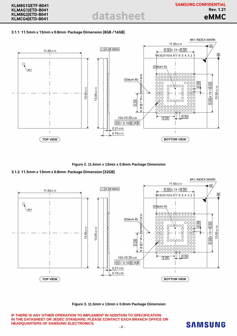
3.1.1 11.5mm x 13mm x 0.8mm Package Dimension
0.08 MAX
0.70±0.10
TOP VIEW
11.50±0.10
#A1
13.0
0±0.1
0
#A1 INDEX MARK
BOTTOM VIEW
0.21±0.05
14 14 27 6 5 389111312 10
0.50 x 13 = 6.50
11.50±0.10A
B
(Datum A)
0.50
13.0
0±0.1
0
0.50
(Datum B)
153-0.30±0.05
0.15 M A B
3.25
ABC
ED
F
HJ
LK
NP
G
M
13.0
0±0.
10
3.25
0.50
x 1
3 =
6.5
0
[8GB /16GB]
Figure 2. 11.5mm x 13mm x 0.8mm Package Dimension
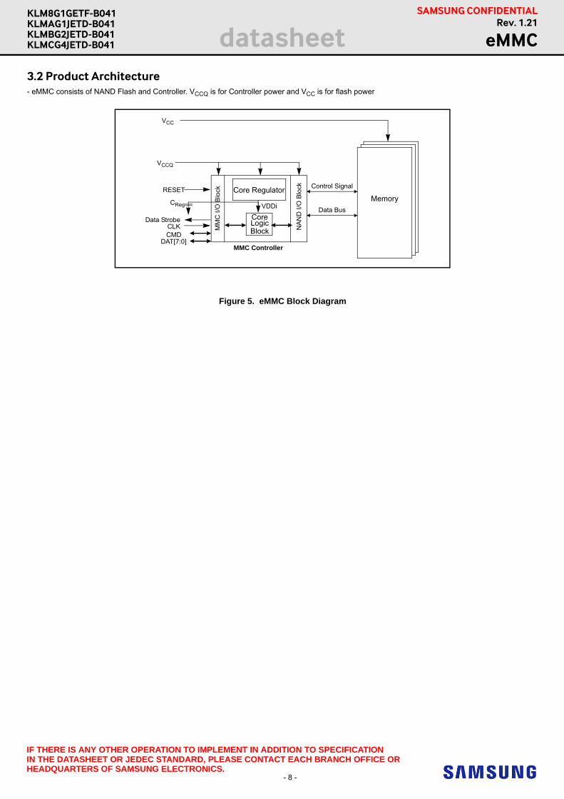
3.1.2 11.5mm x 13mm x 0.8mm Package Dimension
0.08 MAX
0.72±0.08
TOP VIEW
11.50±0.10
#A1
13.0
0±0.1
0
#A1 INDEX MARK
BOTTOM VIEW
0.21±0.05
14 14 27 6 5 389111312 10
0.50 x 13 = 6.50
11.50±0.10A
B
(Datum A)
0.50
13.0
0±0.1
0
0.50
(Datum B)
153-0.30±0.05
0.15 M A B
3.25
ABC
ED
F
HJ
LK
NP
G
M
13.0
0±0.
10
3.25
0.50
x 1
3 =
6.5
0
[32GB]
Figure 3. 11.5mm x 13mm x 0.8mm Package Dimension

- 7 -
IF THERE IS ANY OTHER OPERATION TO IMPLEMENT IN ADDITION TO SPECIFICATIONIN THE DATASHEET OR JEDEC STANDARD, PLEASE CONTACT EACH BRANCH OFFICE OR HEADQUARTERS OF SAMSUNG ELECTRONICS.
datasheet eMMCRev. 1.21
SAMSUNG CONFIDENTIALKLM8G1GETF-B041KLMAG1JETD-B041KLMBG2JETD-B041KLMCG4JETD-B041
3.1.3 11.5mm x 13mm x 1.0mm Package Dimension
0.08 MAX
0.92±0.08
TOP VIEW
11.50±0.10
#A1
13.0
0±0.1
0
#A1 INDEX MARK
BOTTOM VIEW
0.21±0.05
14 14 27 6 5 389111312 10
0.50 x 13 = 6.50
11.50±0.10A
B
(Datum A)
0.50
13.0
0±0.1
0
0.50
(Datum B)
153-0.30±0.05
0.15 M A B
3.25
ABC
ED
F
HJ
LK
NP
G
M
13.0
0±0.
10
3.25
0.50
x 1
3 =
6.5
0
[64GB]
Figure 4. 11.5mm x 13mm x 1.0mm Package Dimension
- 8 -
IF THERE IS ANY OTHER OPERATION TO IMPLEMENT IN ADDITION TO SPECIFICATIONIN THE DATASHEET OR JEDEC STANDARD, PLEASE CONTACT EACH BRANCH OFFICE OR HEADQUARTERS OF SAMSUNG ELECTRONICS.
datasheet eMMCRev. 1.21
SAMSUNG CONFIDENTIALKLM8G1GETF-B041KLMAG1JETD-B041KLMBG2JETD-B041KLMCG4JETD-B041
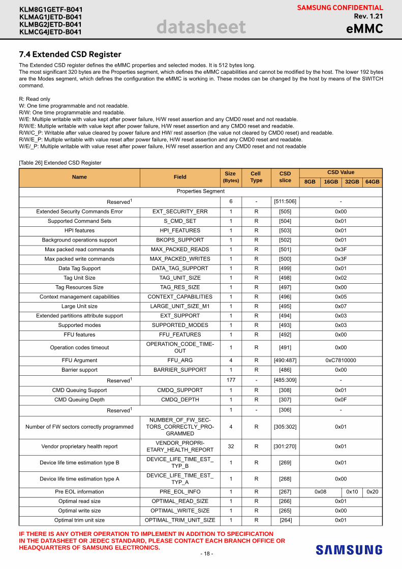
3.2 Product Architecture
Control Signal
Data Bus
MMC Controller
VCC
Core Regulator
Core
Memory
NA
ND
I/O
Blo
ck
MM
C I
/O B
lock
LogicBlock
VCCQ
RESET
VDDi
Data Strobe
CMDDAT[7:0]
CReg
CLK
- eMMC consists of NAND Flash and Controller. VCCQ is for Controller power and VCC is for flash power
Figure 5. eMMC Block Diagram

- 9 -
IF THERE IS ANY OTHER OPERATION TO IMPLEMENT IN ADDITION TO SPECIFICATIONIN THE DATASHEET OR JEDEC STANDARD, PLEASE CONTACT EACH BRANCH OFFICE OR HEADQUARTERS OF SAMSUNG ELECTRONICS.
datasheet eMMCRev. 1.21
SAMSUNG CONFIDENTIALKLM8G1GETF-B041KLMAG1JETD-B041KLMBG2JETD-B041KLMCG4JETD-B041
4.0 HS400 modeeMMC5.0 product supports high speed DDR interface timing mode up to 400MB/s at 200MHz with 1.8V I/O supply.HS400 mode supports the following features : DDR Data sampling methodCLK frequency up to 200MHz DDR (up to 400Mbps) Only 8-bits bus width availableSignaling levels of 1.8V Six selectable Drive Strength (refer to the table below)
[Table 3] I/O driver strength types
NOTE: 1) Support of Driver Type-0 is default for HS200 & HS400 Device, while supporting Driver types 1~4 are optional for HS200 & HS400 Device.
[Table 4] Device type values (EXT_CSD register : DEVICE_TYPE [196])
[Table 5] Extended CSD revisions (EXT_CSD register : EXT_CSD_REV [192])
[Table 6] High speed timing values (EXT_CSD register : HS_TIMING [185])
Driver TypeHS200 & HS400
SupportNominal Impedance
Approximated drivingcapability compared to Type-0
Remark
0 Default 50Ω x1Default Driver Type.Supports up to 200MHz operation.
1 Optional 33Ω x1.5 Supports up to 200MHz Operation.
2 Optional 66Ω x0.75 The weakest driver that supports up to 200MHz operation.
3 Optional 100Ω x0.5For low noise and low EMI systems.Maximal operating frequency is decided by Host design.
4 Optional 40Ω x1.2 Supports up to 200MHz DDR operation
Bit Device Type Supportability
7 HS400 Dual Data Rate eMMC @ 200 MHz - 1.2V I/O Not support
6 HS400 Dual Data Rate eMMC @ 200 MHz - 1.8V I/O Support
5 HS200 Single Data Rate eMMC @ 200 MHz - 1.2V I/O Not support
4 HS200 Single Data Rate eMMC @ 200 MHz - 1.8V I/O Support
3 High-Speed Dual Data Rate eMMC @ 52MHz - 1.2V I/O Not support
2 High-Speed Dual Data Rate eMMC @ 52MHz - 1.8V or 3V I/O Support
1 High-Speed eMMC @ 52MHz - at rated device voltage(s) Support
0 High-Speed eMMC @ 26MHz - at rated device voltage(s) Support
Value Timing Interface EXT_CSD Register Value
255-8 Reserved -
8 Revision 1.8 (for MMC V5.1) 0x08
7 Revision 1.7 (for MMC V5.0) -
6 Revision 1.6 (for MMC V4.5, V4.51) -
5 Revision 1.5 (for MMC V4.41) -
4 Revision 1.4 (Obsolete) -
3 Revision 1.3 (for MMC V4.3) -
2 Revision 1.2 (for MMC V4.2) -
1 Revision 1.1 (for MMC V4.1) -
0 Revision 1.0 (for MMC V4.0) -
Value Timing Interface Supportability
0x0 Selecting backwards compatibility interface timing Support
0x1 High Speed Support
0x2 HS200 Support
0x3 HS400 Support

- 10 -
IF THERE IS ANY OTHER OPERATION TO IMPLEMENT IN ADDITION TO SPECIFICATIONIN THE DATASHEET OR JEDEC STANDARD, PLEASE CONTACT EACH BRANCH OFFICE OR HEADQUARTERS OF SAMSUNG ELECTRONICS.
datasheet eMMCRev. 1.21
SAMSUNG CONFIDENTIALKLM8G1GETF-B041KLMAG1JETD-B041KLMBG2JETD-B041KLMCG4JETD-B041
5.0 New eMMC5.1 Features 5.1 Overview
5.2 Command QueuingTo facilitate command queuing in eMMC, the device manages an internal task queue that the host can queue during data transfer tasks.
Every task is issued by the host and initially queued as pending. The device works to prepare pending tasks for execution. When a task is ready for exe-cution, its state changes to “ready for execution”.
The host tracks the state of all queued tasks and may order the execution of any task, marked as “ready for execution”, by sending a command indicating its task ID. The device executes the data transfer transaction after receiving the execute command(CMD46/CMD47)
5.2.1 CMD Set Description
[Table 7] CMD Set Description and Details
5.2.2 New Response : QSR (Queue Status Register)
The 32-bit Queue Status Register (QSR) carries the state of tasks in the queue at a specific point in time. The host has read access to this register through device response to SEND_STATUS command (CMD13 with bit[15]=”1”), R1’s argument will be the 32- bit Queue Status Register (QSR). Every bit in the QSR represents the task who’s ID corresponds to the bit index. If bit QSR[i] = “0”, then the queued task with a Task ID i is not ready for execution. The task may be queued and pending, or the Task ID is unused. If bit QSR[i] = “1”, then the queued task with Task ID i is ready for execution.
5.2.3 Send Status : CMD13
CMD13 for reading the Queue Status Register (QSR) by the host. If bit[15] in CMD13’s argument is set to 1, then the device shall send an R1 Response with the QSR instead of the Device Status. * There is still legacy CMD13 with R` response
New Feature JEDEC Support
Cache Flushing Report Mandatory Yes
Background operation control Mandatory Yes
Command Queuing Optional Yes
Enhanced Strobe Optional Yes
RPMB Throughput improve Optional Yes
Secure Write Protection Optional Yes
CMD Type Argument Abbreviation Purpose
CMD44 ac/R1
[31] Reliable Write Request[30] DAT_DIR - "0" write / "1" read[29] tag request [28:25] context ID [24] forced programming[23] Priority: “0” simple / “1” high[20:16] TASK ID[15:0] number of blocks
QUEUED_TASK _PARAMSDefine direction of operation (Read or Write) and
Set high priority CMD Queue with task ID
CMD45 ac/R1 [31:0] Start block address QUEUED_TASK_ADDRESS Indicate data address for Queued CMD
CMD46 adtc/R1 [20:16] TASK ID EXECUTE_READ_TASK (Read) Transmit the requested number of data blocks
CMD47 adtc/R1 [20:16] TASK ID EXECUTE_WRITE_TASK (Write) Transmit the requested number of data blocks
CMD48 ac/R1b[20:16] Task ID [3:0] TM op-code
CMDQ_TASK _MGMTReset a specific task or entire queue.
[20:16] when TM op-code = 2h these bits represent TaskID. When TM op-code = 1h these bits are reserved."

- 11 -
IF THERE IS ANY OTHER OPERATION TO IMPLEMENT IN ADDITION TO SPECIFICATIONIN THE DATASHEET OR JEDEC STANDARD, PLEASE CONTACT EACH BRANCH OFFICE OR HEADQUARTERS OF SAMSUNG ELECTRONICS.
datasheet eMMCRev. 1.21
SAMSUNG CONFIDENTIALKLM8G1GETF-B041KLMAG1JETD-B041KLMBG2JETD-B041KLMCG4JETD-B041
5.2.4 Mechanism of CMD Queue operation
Host issues CMD44 with Task ID number, Sector, Count, Direction, Priority to the device followed by CMD45 and host checks the Queue Status check with CMD13 [15]bits to 1 . After that host issues CMD46 for Read or CMD47 for write During CMD queue operation, CMD44/CMD45 is able to be issued at anytime when the CMD line is not in use
5.2.5 CMD Queue Register description
Configuration and capability structures shall be added to the EXT_CSD register, as described below
[Table 8] CMD Queuing Support (EXT_CSD register : CMDQ_SUPPORT [308])
This field indicates whether the device supports command queuing or not
0x0: CMD Queue function is not supported0x1: CMD Queue function is supported
[Table 9] Command Queue Mode Enable(EXT_CSD register : CMDQ_MODE_EN [15])
This field is used by the host enable command queuing
0x0: Queue function is not enabled0x1: Queue function is enabled
[Table 10] CMD Queuing Depth(EXT_CSD register : CMDQ_DEPTH [307])
This field is used to calculate the depth of the queue supported by the device
Bit encoding:[7:5]: Reserved[4:0]: N,a parameter used to calculate the Queue Depth of task queue in the device.Queue Depth = N+1.
5.3 Enhanced Strobe ModeThis product supports Enhanced Strobe in HS400 mode and refer to the details as described in eMMC5.1 JEDEC standard
5.4 RPMB Throughput improve
[Table 11] Related parameter register in EXT_CSD : WR_REL_PARAM [166]
Bit[4]: EN_RPMB_REL_WR(R) 0x0: RPMB transfer size is either 256B (single 512B frame) or 512B (Two 512B frame). 0 x1: RPMB transfer size is either 256B (single 512B frame), 512B (Two 512B frame), or 8KB(Thirthy two 512B frames).
Bit7 Bit6 Bit5 Bit4 Bit 3 Bit2 Bit1 Bit0
Reserved CMD Queue supportability
Bit7 Bit6 Bit5 Bit4 Bit 3 Bit2 Bit1 Bit0
Reserved 0x00
Bit7 Bit6 Bit5 Bit4 Bit 3 Bit2 Bit1 Bit0
Reserved 0x0F
Name Field Bit Type
Enhanced RPMB Reliable Write EN_RPMB_REL_WR 4 R
CMD
DATA
44 R1 45 R1R1 44 45 R1 13 QSR
46 R1
47 R1
R144 45 R1 13 QSR
Data Data
*Read Execution
*Write Execution

- 12 -
IF THERE IS ANY OTHER OPERATION TO IMPLEMENT IN ADDITION TO SPECIFICATIONIN THE DATASHEET OR JEDEC STANDARD, PLEASE CONTACT EACH BRANCH OFFICE OR HEADQUARTERS OF SAMSUNG ELECTRONICS.
datasheet eMMCRev. 1.21
SAMSUNG CONFIDENTIALKLM8G1GETF-B041KLMAG1JETD-B041KLMBG2JETD-B041KLMCG4JETD-B041
5.5 Secure Write ProtectionConfiguration and capability structures shall be added to the EXT_CSD register and Authenticated Device Configuration Area as described below
[Table 12] Parameter register in EXT_CSD : SECURE_WP_INFO [211]
Bit[7:2]: ReservedBit[1]: SECURE_WP_EN_STATUS(R) 0x0: Legacy Write Protection mode. 0x1: Secure Write Protection mode.Bit[0]: SECURE_WP_SUPPORT(R) 0x0: Secure Write Protection is NOT supported by this device 0x1: Secure Write Protection is supported by this device
[Table 13] Authenticated Device Configuration Area[1] : SECURE_WP_MODE_ENABLE
Bit[7:1] : ReservedBit[0] : SECURE_WP_EN (R/W/E)The default value of this field is 0x0.
0x0 : Legacy Write Protection mode, i.e., TMP_WRITE_PROTECT[12] , PERM_WRITE_PROTECT[13] is updated by CMD27. USER_WP[171], BOOT_WP[173] and BOOT_WP_STATUS[174] are updated by CMD6.
0x1 : Secure Write Protection mode. The access to the write protection related EXT_CSD and CSD fields depends on the value of SECURE_WP_MASK bit in SECURE_WP_MODE_CONFIG field.
[Table 14] Authenticated Device Configuration Area[2] : SECURE_WP_MODE_CONFIG
Bit[7:1] : ReservedBit[0] : SECURE_WP_MASK (R/W/E_P)The default value of this field is 0x0.
0x0: Disabling updating WP related EXT_CSD and CSD fields. CMD27 (Program CSD) will generate generic error for setting TMP_WRITE_PROTECT[12] , PERM_WRITE_PROTECT[13]. CMD6 for updating USER_WP[171], BOOT_WP[173] and BOOT_WP_STATUS[174] generates SWITCH_ERROR. If a force erase command is issued, the command will fail (Device stays locked) and the LOCK_UNLOCK_FAILED error bit will be set in the status register. If CMD28 or CMD29 is issued, then generic error will be occurred. Power-on Write Protected boot partitions will keep protected mode after power failure, H/W reset assertion and any CMD0 reset. The device keeps the current value of BOOT_WP_STATUS in the EXT_CSD register to be same after power cycle, H/W reset assertion, and any CMD0 reset.
0x1: Enabling updating WP related EXT_CSD and CSD fields. I.e TMP_WRITE_PROTECT[12] , PERM_WRITE_PROTECT[13] , USER_WP[171], BOOT_WP[173] and BOOT_WP_STATUS[174] are accessed using CMD6, CMD8 and CMD27. If a force erase command is issued and accepted, then ALL THE DEVICE CONTENT WILL BE ERASED including the PWD and PWD_LEN register content and the locked Device will get unlocked. If a force erase command is issued and power-on protected or a permanently-write- protected write protect groups exist on the device, the command will fail (Device stays locked) and the LOCK_UNLOCK_FAILED error bit will be set in the status register. An attempt to force erase on an unlocked Device will fail and LOCK_UNLOCK_FAILED error bit will be set in the status register. Write Protection is applied to the WPG indicated by CMD28 with the WP type indicated by the bit[2] and bit[0] of USER_WP[171]. All temporary WP Groups and power-on Write Protected boot partitions become writable/erasable temporarily which means write protect type is not changed. All power-on and permanent WP Groups in user area will not become writable/erasable temporarily. Those temporarily writable/erasable area will become write protected when this bit is cleared to 0x0 by the host or when there is power failure, H/W reset assertion and any CMD0 reset. The device keeps the current value of BOOT_WP_STATUS in the EXT_CSD register to be same after power cycle, H/W reset assertion, and any CMD0 reset.
Bit7 Bit6 Bit5 Bit4 Bit Bit2 Bit1 Bit0
Reserved SECURE_WP_EN_STATUS SECURE_WP_SUPPORT
Bit7 Bit6 Bit5 Bit4 Bit Bit2 Bit1 Bit0
Reserved 0x00
Bit7 Bit6 Bit5 Bit4 Bit Bit2 Bit1 Bit0
Reserved 0x00

- 13 -
IF THERE IS ANY OTHER OPERATION TO IMPLEMENT IN ADDITION TO SPECIFICATIONIN THE DATASHEET OR JEDEC STANDARD, PLEASE CONTACT EACH BRANCH OFFICE OR HEADQUARTERS OF SAMSUNG ELECTRONICS.
datasheet eMMCRev. 1.21
SAMSUNG CONFIDENTIALKLM8G1GETF-B041KLMAG1JETD-B041KLMBG2JETD-B041KLMCG4JETD-B041
6.0 Technical Notes6.1 S/W Algorithm6.1.1 Partition Management
The device initially consists of two Boot Partitions and RPMB Partition and User Data Area.
The User Data Area can be divided into four General Purpose Area Partitions and User Data Area partition. Each of the General Purpose Area partitions and a section of User Data Area partition can be configured as enhanced partition.
6.1.1.1 Enhanced Partition (Area)
SAMSUNG eMMC adopts Enhanced User Data Area as SLC Mode. Therefore when master adopts some portion as enhanced user data area in User Data Area, that area occupies double size of original set up size. ( ex> if master set 1MB for enhanced mode, total 2MB user data area is needed to gen-erate 1MB enhanced area)
Max Enhanced User Data Area size is defined as (MAX_ENH_SIZE_MULT x HC_WP_GRP_SIZE x HC_ERASE_GRP_SIZE x 512kBytes)
6.1.2 Boot operation
Device supports not only boot mode but also alternative boot mode. Device supports high speed timing and dual data rate during boot.
Figure 6. embedded MultiMediaCard state diagram (boot mode)
Figure 7. embedded MultiMediaCard state diagram (alternative boot mode)
[Table 15] Boot ack, boot data and initialization Time
NOTE: 1) This initialization time includes partition setting, Please refer to INI_TIMEOUT_AP in 6.4 Extended CSD Register. Normal initialization time (without partition setting) is completed within 1sec
Timing Factor Value
(1) Boot ACK Time < 50 ms
(2) Boot Data Time < 100 ms
(3) Initialization Time1) < 3 secs
S E S E010512bytes+CRC
CLK
CMD
DAT[0]
CMD1 RESP CMD2 RESP
Boot terminated
MIn 8 cloks + 48 clocks = 56 clocks required fromCMD signal high to next MMC command.
(1)
(2)
*(1) Boot ACK Time (2) Boot Data Time
S E S E010512bytes+CRC
CLK
CMD
DAT[0]
CMD1 RESP CMD2CMD01 CMD0 Reset
Min74Clocks requiredafterpower isstable to start bootcommand
*(1) Boot ACK Time (2) Boot Data Time (3) CMD1 Time*CMD0 with argument 0xFFFFFFFA
(1)
(2)
Boot terminated
CMD1
(3)

- 14 -
IF THERE IS ANY OTHER OPERATION TO IMPLEMENT IN ADDITION TO SPECIFICATIONIN THE DATASHEET OR JEDEC STANDARD, PLEASE CONTACT EACH BRANCH OFFICE OR HEADQUARTERS OF SAMSUNG ELECTRONICS.
datasheet eMMCRev. 1.21
SAMSUNG CONFIDENTIALKLM8G1GETF-B041KLMAG1JETD-B041KLMBG2JETD-B041KLMCG4JETD-B041
6.1.3 User Density
Total User Density depends on device type. For example, 32MB in the SLC Mode requires 64MB in MLC.This results in decreasing of user density
[Table 16] Capacity according to partition
[Table 17] Maximum Enhanced Partition Size
[Table 18] User Density Size
Boot partition 1 Boot partition 2 RPMB
8GBDefault. 4,096KB 4,096KB 512KB
Max. 4,096KB 4,096KB 4,096KB
16GB/32GB/64GBDefault. 4,096KB 4,096KB 4,096KB
Max. 4,096KB 4,096KB 4,096KB
Device Max. Enhanced Partition Size
8 GB 3,909,091,328 Byte
16 GB 7,809,794,048 Byte
32 GB 15,627,976,704 Byte
64 GB 31,264,342,016 Byte
Device User Density Size
8 GB 7,818,182,656 Byte
16 GB 15,634,268,160 Byte
32 GB 31,268,536,320 Byte
64 GB 62,537,072,640 Byte
4321
User Density
Enhanced User Data Area4 General Purpose Partitions (GPP)RPMBBoot Partition #1 

- 15 -
IF THERE IS ANY OTHER OPERATION TO IMPLEMENT IN ADDITION TO SPECIFICATIONIN THE DATASHEET OR JEDEC STANDARD, PLEASE CONTACT EACH BRANCH OFFICE OR HEADQUARTERS OF SAMSUNG ELECTRONICS.
datasheet eMMCRev. 1.21
SAMSUNG CONFIDENTIALKLM8G1GETF-B041KLMAG1JETD-B041KLMBG2JETD-B041KLMCG4JETD-B041
6.1.4 Auto Power Saving Mode
If host does not issue any command during a certain duration (1ms), after previously issued command is completed, the device enters "Power Saving mode" to reduce power consumption.
At this time, commands arriving at the device while it is in power saving mode will be serviced in normal fashion
[Table 19] Auto Power Saving Mode and exit
[Table 20] Auto Power Saving Mode and Sleep Mode
6.1.5 Performance
[Table 21] Performance
* Test Condition : Bus width x8, HS400, 512KB data transfer, w/o file system overhead, measured on Samsung’s internal board
Mode Enter Condition Escape Condition
Auto Power Saving ModeWhen previous operation which came from Host is completed and no com-mand is issued during a certain time.
If Host issues any command
Auto Power Saving Mode Sleep Mode
NAND Power ON OFF
Goto Sleep Time < 1ms < 1ms
Density Sequential Read (MB/s) Sequential Write (MB/s)
8 GB
330
5016 GB
32 GB 100
64 GB 200

- 16 -
IF THERE IS ANY OTHER OPERATION TO IMPLEMENT IN ADDITION TO SPECIFICATIONIN THE DATASHEET OR JEDEC STANDARD, PLEASE CONTACT EACH BRANCH OFFICE OR HEADQUARTERS OF SAMSUNG ELECTRONICS.
datasheet eMMCRev. 1.21
SAMSUNG CONFIDENTIALKLM8G1GETF-B041KLMAG1JETD-B041KLMBG2JETD-B041KLMCG4JETD-B041
7.0 REGISTER VALUE7.1 OCR RegisterThe 32-bit operation conditions register stores the VCCQ voltage profile of the eMMC. In addition, this register includes a status information bit. This status
bit is set if the eMMC power up procedure has been finished. The OCR register shall be implemented by all eMMCs.
[Table 22] OCR Register
NOTE :1) This bit is set to LOW if the eMMC has not finished the power up routine 2) The voltage for internal flash memory(VCC) should be 2.7-3.6v regardless of OCR Register value.
7.2 CID Register[Table 23] CID Register
NOTE :1),4),5) description are same as eMMC JEDEC standard2) PRV is composed of the revision count of controller and the revision count of F/W patch 3) A 32 bits unsigned binary integer. (Random Number)
7.2.1 Product name table (In CID Register)
[Table 24] Product name table
OCR bit VCCQ voltage window2 Register Value
[6:0] Reserved 00 00000b
[7] 1.70 - 1.95 1b
[14:8] 2.0-2.6 000 0000b
[23:15] 2.7-3.6 1 1111 1111b
[28:24] Reserved 0 0000b
[30:29] Access Mode 00b (byte mode) 10b (sector mode) -[ *Higher than 2GB only]
[31] eMMC power up status bit (busy)1
Name Field Width CID-slice CID Value
Manufacturer ID MID 8 [127:120] 0x15
Reserved 6 [119:114] ---
Card/BGA CBX 2 [113:112] 01
OEM/Application ID OID 8 [111:104] ---1
Product name PNM 48 [103:56] See Product name table
Product revision PRV 8 [55:48] ---2
Product serial number PSN 32 [47:16] ---3
Manufacturing date MDT 8 [15:8] ---4
CRC7 checksum CRC 7 [7:1] ---5
not used, always ’1’ - 1 [0:0] ---
Part Number Density Product Name in CID Register (PNM)
KLM8G1GETF-B041 8 GB 0 x 384754463452
KLMAG1JETD-B041 16 GB 0 x 414A54443452
KLMBG2JETD-B041 32 GB 0 x 424A54443452
KLMCG4JETD-B041 64 GB 0 x 434A54443452

- 17 -
IF THERE IS ANY OTHER OPERATION TO IMPLEMENT IN ADDITION TO SPECIFICATIONIN THE DATASHEET OR JEDEC STANDARD, PLEASE CONTACT EACH BRANCH OFFICE OR HEADQUARTERS OF SAMSUNG ELECTRONICS.
datasheet eMMCRev. 1.21
SAMSUNG CONFIDENTIALKLM8G1GETF-B041KLMAG1JETD-B041KLMBG2JETD-B041KLMCG4JETD-B041
7.3 CSD RegisterThe Card-Specific Data register provides information on how to access the eMMC contents. The CSD defines the data format, error correction type, max-imum data access time, data transfer speed, whether the DSR register can be used etc. The programmable part of the register (entries marked by W or E, see below) can be changed by CMD27. The type of the entries in the table below is coded as follows:R: Read onlyW: One time programmable and not readable.R/W: One time programmable and readable.W/E: Multiple writable with value kept after power failure, H/W reset assertion and any CMD0 reset and not readable.R/W/E: Multiple writable with value kept after power failure, H/W reset assertion and any CMD0 reset and readable.R/W/C_P: Writable after value cleared by power failure and HW/ rest assertion (the value not cleared by CMD0 reset) and readable.R/W/E_P: Multiple writable with value reset after power failure, H/W reset assertion and any CMD0 reset and readable.
W/E/_P: Multiple writable with value reset after power failure, H/W reset assertion and any CMD0 reset and not readable.
[Table 25] CSD Register
Name Field Width Cell Type CSD-slice CSD Value
8GB 16 GB 32 GB 64 GB
CSD structure CSD_STRUCTURE 2 R [127:126] 0x03
System specification version SPEC_VERS 4 R [125:122] 0x04
Reserved - 2 R [121:120] -
Data read access-time 1 TAAC 8 R [119:112] 0x27
Data read access-time 2 in CLK cycles (NSAC*100) NSAC 8 R [111:104] 0x01
Max. bus clock frequency TRAN_SPEED 8 R [103:96] 0x32
Device command classes CCC 12 R [95:84] 0xF5
Max. read data block length READ_BL_LEN 4 R [83:80] 0x09
Partial blocks for read allowed READ_BL_PARTIAL 1 R [79:79] 0x00
Write block misalignment WRITE_BLK_MISALIGN 1 R [78:78] 0x00
Read block misalignment READ_BLK_MISALIGN 1 R [77:77] 0x00
DSR implemented DSR_IMP 1 R [76:76] 0x00
Reserved - 2 R [75:74] -
Device size C_SIZE 12 R [73:62] 0xFFF
Max. read current @ VDD min VDD_R_CURR_MIN 3 R [61:59] 0x06
Max. read current @ VDD max VDD_R_CURR_MAX 3 R [58:56] 0x06
Max. write current @ VDD min VDD_W_CURR_MIN 3 R [55:53] 0x06
Max. write current @ VDD max VDD_W_CURR_MAX 3 R [52:50] 0x06
Device size multiplier C_SIZE_MULT 3 R [49:47] 0x07
Erase group size ERASE_GRP_SIZE 5 R [46:42] 0x1F
Erase group size multiplier ERASE_GRP_MULT 5 R [41:37] 0x1F
Write protect group size WP_GRP_SIZE 5 R [36:32] 0x0F
Write protect group enable WP_GRP_ENABLE 1 R [31:31] 0x01
Manufacturer default ECC DEFAULT_ECC 2 R [30:29] 0x00
Write speed factor R2W_FACTOR 3 R [28:26] 0x03
Max. write data block length WRITE_BL_LEN 4 R [25:22] 0x09
Partial blocks for write allowed WRITE_BL_PARTIAL 1 R [21:21] 0x00
Reserved - 4 R [20:17] -
Content protection application CONTENT_PROT_APP 1 R [16:16] 0x00
File format group FILE_FORMAT_GRP 1 R/W [15:15] 0x00
Copy flag (OTP) COPY 1 R/W [14:14] 0x01
Permanent write protection PERM_WRITE_PROTECT 1 R/W [13:13] 0x00
Temporary write protection TMP_WRITE_PROTECT 1 R/W/E [12:12] 0x00
File format FILE_FORMAT 2 R/W [11:10] 0x00
ECC code ECC 2 R/W/E [9:8] 0x00
CRC CRC 7 R/W/E [7:1] -
Not used, always’1’ - 1 — [0:0] -
- 18 -
IF THERE IS ANY OTHER OPERATION TO IMPLEMENT IN ADDITION TO SPECIFICATIONIN THE DATASHEET OR JEDEC STANDARD, PLEASE CONTACT EACH BRANCH OFFICE OR HEADQUARTERS OF SAMSUNG ELECTRONICS.
datasheet eMMCRev. 1.21
SAMSUNG CONFIDENTIALKLM8G1GETF-B041KLMAG1JETD-B041KLMBG2JETD-B041KLMCG4JETD-B041
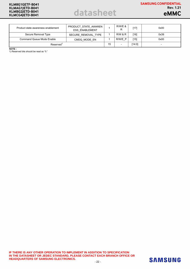
7.4 Extended CSD RegisterThe Extended CSD register defines the eMMC properties and selected modes. It is 512 bytes long.The most significant 320 bytes are the Properties segment, which defines the eMMC capabilities and cannot be modified by the host. The lower 192 bytes are the Modes segment, which defines the configuration the eMMC is working in. These modes can be changed by the host by means of the SWITCH command.
R: Read onlyW: One time programmable and not readable.R/W: One time programmable and readable.W/E: Multiple writable with value kept after power failure, H/W reset assertion and any CMD0 reset and not readable.R/W/E: Multiple writable with value kept after power failure, H/W reset assertion and any CMD0 reset and readable.R/W/C_P: Writable after value cleared by power failure and HW/ rest assertion (the value not cleared by CMD0 reset) and readable.R/W/E_P: Multiple writable with value reset after power failure, H/W reset assertion and any CMD0 reset and readable.W/E/_P: Multiple writable with value reset after power failure, H/W reset assertion and any CMD0 reset and not readable
[Table 26] Extended CSD Register
Name Field Size
(Bytes) Cell Type
CSDslice
CSD Value
8GB 16GB 32GB 64GB
Properties Segment
Reserved1 6 - [511:506] -
Extended Security Commands Error EXT_SECURITY_ERR 1 R [505] 0x00
Supported Command Sets S_CMD_SET 1 R [504] 0x01
HPI features HPI_FEATURES 1 R [503] 0x01
Background operations support BKOPS_SUPPORT 1 R [502] 0x01
Max packed read commands MAX_PACKED_READS 1 R [501] 0x3F
Max packed write commands MAX_PACKED_WRITES 1 R [500] 0x3F
Data Tag Support DATA_TAG_SUPPORT 1 R [499] 0x01
Tag Unit Size TAG_UNIT_SIZE 1 R [498] 0x02
Tag Resources Size TAG_RES_SIZE 1 R [497] 0x00
Context management capabilities CONTEXT_CAPABILITIES 1 R [496] 0x05
Large Unit size LARGE_UNIT_SIZE_M1 1 R [495] 0x07
Extended partitions attribute support EXT_SUPPORT 1 R [494] 0x03
Supported modes SUPPORTED_MODES 1 R [493] 0x03
FFU features FFU_FEATURES 1 R [492] 0x00
Operation codes timeoutOPERATION_CODE_TIME-
OUT1 R [491] 0x00
FFU Argument FFU_ARG 4 R [490:487] 0xC7810000
Barrier support BARRIER_SUPPORT 1 R [486] 0x00
Reserved1 177 - [485:309] -
CMD Queuing Support CMDQ_SUPPORT 1 R [308] 0x01
CMD Queuing Depth CMDQ_DEPTH 1 R [307] 0x0F
Reserved1 1 - [306] -
Number of FW sectors correctly programmedNUMBER_OF_FW_SEC-
TORS_CORRECTLY_PRO-GRAMMED
4 R [305:302] 0x01
Vendor proprietary health reportVENDOR_PROPRI-
ETARY_HEALTH_REPORT32 R [301:270] 0x01
Device life time estimation type BDEVICE_LIFE_TIME_EST_
TYP_B1 R [269] 0x01
Device life time estimation type ADEVICE_LIFE_TIME_EST_
TYP_A1 R [268] 0x00
Pre EOL information PRE_EOL_INFO 1 R [267] 0x08 0x10 0x20
Optimal read size OPTIMAL_READ_SIZE 1 R [266] 0x01
Optimal write size OPTIMAL_WRITE_SIZE 1 R [265] 0x00
Optimal trim unit size OPTIMAL_TRIM_UNIT_SIZE 1 R [264] 0x01

- 19 -
IF THERE IS ANY OTHER OPERATION TO IMPLEMENT IN ADDITION TO SPECIFICATIONIN THE DATASHEET OR JEDEC STANDARD, PLEASE CONTACT EACH BRANCH OFFICE OR HEADQUARTERS OF SAMSUNG ELECTRONICS.
datasheet eMMCRev. 1.21
SAMSUNG CONFIDENTIALKLM8G1GETF-B041KLMAG1JETD-B041KLMBG2JETD-B041KLMCG4JETD-B041
Device version DEVICE_VERSION 1 R [263:262] 0x00
Firmware version FIRMWARE_VERSION 3 R [261:254] 0x01
Power class for 200MHz, DDR at VCC=3.6V PWR_CL_DDR_200_360 1 R [253] 0x00
Cache size CACHE_SIZE 4 R [252:249] 0x10000
Generic CMD6 timeout GENERIC_CMD6_TIME 1 R [248] 0x0A
Power off notification (long) timeout POWER_OFF_LONG_TIME 1 R [247] 0x3C
Background operations status BKOPS_STATUS 1 R [246] 0x00
Number of correctly programmed sectors CORRECTLY_PRG_SEC-
TORS_NUM 4 R [245:242] 0x00
1st initialization time after partitioning INI_TIMEOUT_AP 1 R [241] 0x1E
Cache flush policy CACHE_FLUSH_POLICY 1 R [240] -
Power class for 52MHz, DDR at 3.6V PWR_CL_DDR_52_360 1 R [239] 0x00
Power class for 52MHz, DDR at 1.95V PWR_CL_DDR_52_195 1 R [238] 0x00
Power class for 200MHz at VCCQ=1.95V, VCC=3.6V PWR_CL_200_360 1 R [237] 0x00
Power class for 200MHz, at VCCQ=1.3V, VCC=3.6V PWR_CL_200_195 1 R [236] 0x00
Minimum Write Performance for 8bit at 52MHzin DDR mode
MIN_PERF_DDR_W_8_52 1 R [235] 0x00
Minimum Read Performance for 8bit at 52MHz in DDR mode
MIN_PERF_DDR_R_8_52 1 R [234] 0x00
Reserved1 1 - [233] -
TRIM Multiplier TRIM_MULT 1 R [232] 0x02
Secure Feature support SEC_FEATURE_SUPPORT 1 R [231] 0x55
Secure Erase Multiplier SEC_ERASE_MULT 1 R [230] 0x1B
Secure TRIM Multiplier SEC_TRIM_MULT 1 R [229] 0x11
Boot information BOOT_INFO 1 R [228] 0x07
Reserved1 1 - [227] -
Boot partition size BOOT_SIZE_MULT 1 R [226] 0x20
Access size ACC_SIZE 1 R [225] 0x07
High-capacity erase unit size HC_ERASE_GRP_SIZE 1 R [224] 0x01
High-capacity erase timeout ERASE_TIMEOUT_MULT 1 R [223] 0x01
Reliable write sector count REL_WR_SEC_C 1 R [222] 0x01
High-capacity write protect group size HC_WP_GRP_SIZE 1 R [221] 0x10
Sleep current (VCC) S_C_VCC 1 R [220] 0x07
Sleep current (VCCQ) S_C_VCCQ 1 R [219] 0x07
Production state awareness timeoutPRODUC-
TION_STATE_AWARENESS_-TIMEOUT
1 R [218] 0x00
Sleep/awake timeout S_A_TIMEOUT 1 R [217] 0x11
Sleep Notification Timeout SLEEP_NOTIFICATION_TIME 1 R [216] 0x07
Sector Count SEC_COUNT 4 R [215:212] 0xE90
0000x1D1F000
0x3A3E000
0x747C000
Secure Write Protect Information SECURE_WP_INFO 1 R [211] 0x01
Minimum Write Performance for 8bit at 52MHz
MIN_PERF_W_8_52 1 R [210] 0x00
Minimum Read Performance for 8bit at 52MHz
MIN_PERF_R_8_52 1 R [209] 0x00
Minimum Write Performance for 8bit at26MHz, for 4bit at 52MHz
MIN_PERF_W_8_26_4_52 1 R [208] 0x00
Minimum Read Performance for 8bit at 26MHz, for 4bit at 52MHz
MIN_PERF_R_8_26_4_52 1 R [207] 0x00

- 20 -
IF THERE IS ANY OTHER OPERATION TO IMPLEMENT IN ADDITION TO SPECIFICATIONIN THE DATASHEET OR JEDEC STANDARD, PLEASE CONTACT EACH BRANCH OFFICE OR HEADQUARTERS OF SAMSUNG ELECTRONICS.
datasheet eMMCRev. 1.21
SAMSUNG CONFIDENTIALKLM8G1GETF-B041KLMAG1JETD-B041KLMBG2JETD-B041KLMCG4JETD-B041
Minimum Write Performance for 4bit at 26MHz
MIN_PERF_W_4_26 1 R [206] 0x00
Minimum Read Performance for 4bit at 26MHz
MIN_PERF_R_4_26 1 R [205] 0x00
Reserved1 1 - [204] -
Power class for 26MHz at 3.6V 1 R PWR_CL_26_360 1 R [203] 0x00
Power class for 52MHz at 3.6V 1 R PWR_CL_52_360 1 R [202] 0x00
Power class for 26MHz at 1.95V 1 R PWR_CL_26_195 1 R [201] 0x00
Power class for 52MHz at 1.95V 1 R PWR_CL_52_195 1 R [200] 0x00
Partition switching timing PARTITION_SWITCH_TIME 1 R [199] 0x02
Out-of-interrupt busy timing OUT_OF_INTERRUPT_TIME 1 R [198] 0x0A
I/O Driver Strength DRIVER_STRENGTH 1 R [197] 0x1F
Device type DEVICE_TYPE 1 R [196] 0x57
Reserved1 1 - [195] -
CSD structure CSD_STRUCTURE 1 R [194] 0x02
Reserved1 1 - [193] -
Extended CSD revision EXT_CSD_REV 1 R [192] 0x08
Modes Segment
Command set CMD_SET 1 R/W/E_P [191] 0x00
Reserved1 1 - [190] -
Command set revision CMD_SET_REV 1 R [189] 0x00
Reserved1 1 - [188] -
Power class POWER_CLASS 1 R/W/E_P [187] 0x00
Reserved1 1 - [186] -
High-speed interface timing HS_TIMING 1 R/W/E_P [185] 0x01 0x00
Strobe Support STROBE_SUPPORT 1 R [184] 0x01
Bus width mode BUS_WIDTH 1 W/E_P [183] 0x00
Reserved1 1 - [182] -
Erased memory content ERASED_MEM_CONT 1 R [181] 0x00
Reserved1 1 - [180] -
Partition configuration PARTITION_CONFIG 1 R/W/E & R/W/E_P
[179] 0x00
Boot config protection BOOT_CONFIG_PROT 1 R/W &
R/W/C_P [178] 0x00
Boot bus Conditions BOOT_BUS_CONDITIONS 1 R/W/E [177] 0x0
Reserved1 1 - [176] -
High-density erase group definition ERASE_GROUP_DEF 1 R/W/E_P [175] 0x00
Boot write protection status registers BOOT_WP_STATUS 1 R [174] 0x00
Boot area write protection register BOOT_WP 1 R/W &
R/W/C_P [173] 0x00
Reserved1 1 - [172] -
User area write protection register USER_WP 1
R/W, R/W/C_P
&R/W/E_P
[171] 0x00
Reserved1 1 - [170] -
FW configuration FW_CONFIG 1 R/W [169] 0x00
RPMB Size RPMB_SIZE_MULT 1 R [168] 0x04 0x20
Write reliability setting register WR_REL_SET 1 R/W [167] 0x1F
Write reliability parameter register WR_REL_PARAM 1 R [166] 0x14
Start Sanitize operation SANITIZE_START 1 W/E_P [165] 0x00

- 21 -
IF THERE IS ANY OTHER OPERATION TO IMPLEMENT IN ADDITION TO SPECIFICATIONIN THE DATASHEET OR JEDEC STANDARD, PLEASE CONTACT EACH BRANCH OFFICE OR HEADQUARTERS OF SAMSUNG ELECTRONICS.
datasheet eMMCRev. 1.21
SAMSUNG CONFIDENTIALKLM8G1GETF-B041KLMAG1JETD-B041KLMBG2JETD-B041KLMCG4JETD-B041
Manually start background operations BKOPS_START 1 W/E_P [164] 0x00
Enable background operationshandshake
BKOPS_EN 1R/W&R/
W/E[163] 0x00
H/W reset function RST_n_FUNCTION 1 R/W [162] 0x00
HPI management HPI_MGMT 1 R/W/E_P [161] 0x00
Partitioning Support PARTITIONING_SUPPORT 1 R [160] 0x07
Max Enhanced Area Size MAX_ENH_SIZE_MULT 3 R [159:157] 0x1D2 0x3A3 0x747 0xE8F
Partitions attribute PARTITIONS_ATTRIBUTE 1 R/W [156] 0x00
Partitioning Setting PARTITION_SETTING_
COMPLETED 1 R/W [155] 0x00
General Purpose Partition Size GP_SIZE_MULT 12 R/W [154:143] 0x00
Enhanced User Data Area Size ENH_SIZE_MULT 3 R/W [142:140] 0x00
Enhanced User Data Start Address ENH_START_ADDR 4 R/W [139:136] 0x00
Reserved1 1 - [135] -
Bad Block Management mode SEC_BAD_BLK_MGMNT 1 R/W [134] 0x00
Production state awarenessPRODUC-
TION_STATE_AWARENESS1 W/E_P [133] 0x00
Package Case Temperature iscontrolled
TCASE_SUPPORT 1 W/E_P [132] 0x00
Periodic Wake-up PERIODIC_WAKEUP 1 R/W/E [131] 0x00
Program CID/CSD in DDR mode support PROGRAM_CID_CSD_DDR_-
SUPPORT 1 R [130] 0x01
Reserved1 2 - [129:128] -
Vendor Specific Fields VENDOR_SPECIFIC_FIELD 64<ven-dor spe-cific>
[127:64] -
Native sector size NATIVE_SECTOR_SIZE 1 R [63] 0x00
Sector size emulation USE_NATIVE_SECTOR 1 R/W [62] 0x00
Sector size DATA_SECTOR_SIZE 1 R [61] 0x00
1st initialization after disabling sector size emula-tion
INI_TIMEOUT_EMU 1 R [60] 0x00
Class 6 commands control CLASS_6_CTRL 1 R/W/E_P [59] 0x00
Number of addressed group to be Released DYNCAP_NEEDED 1 R [58] 0x00
Exception events control EXCEPTION_EVENTS_CTRL 2 R/W/E_P [57:56] 0x00
Exception events status EXCEPTION_EVENTS_STA-
TUS 2 R [55:54] 0x00
Extended Partitions Attribute EXT_PARTITIONS_ATTRI-
BUTE 2 R/W [53:52] 0x00
Context configuration CONTEXT_CONF 15 R/W/E_P [51:37] 0x00
Packed command status PACKED_COMMAND_STA-
TUS 1 R [36] 0x00
Packed command failure index PACKED_FAILURE_INDEX 1 R [35] 0x00
Power Off Notification POWER_OFF_NOTIFICATION 1 R/W/E_P [34] 0x00
Control to turn the Cache ON/OFF CACHE_CTRL 1 R/W/E_P [33] 0x00
Flushing of the cache FLUSH_CACHE 1 W/E_P [32] 0x00
Control to turn the Barrier ON/OFF BARRIER_CTRL 1 R [31] 0x00
Mode config MODE_CONFIG 1 R/W/E_P [30] 0x00
Mode operation codes MODE_OPERATION_CODES 1 W/E_P [29] 0x00
Reserved1 2 - [28:27] -
FFU status FFU_STATUS 1 R [26] 0x00
Pre loading data size PRE_LOADING_DATA_SIZE 4 R/W/E_P [25:22] 0x00
Max pre loading data size MAX_PRE_LOADING_DATA_SIZE
4 R [21:18] 0x00
- 22 -
IF THERE IS ANY OTHER OPERATION TO IMPLEMENT IN ADDITION TO SPECIFICATIONIN THE DATASHEET OR JEDEC STANDARD, PLEASE CONTACT EACH BRANCH OFFICE OR HEADQUARTERS OF SAMSUNG ELECTRONICS.
datasheet eMMCRev. 1.21
SAMSUNG CONFIDENTIALKLM8G1GETF-B041KLMAG1JETD-B041KLMBG2JETD-B041KLMCG4JETD-B041
NOTE : 1) Reserved bits should be read as “0.”
Product state awareness enablement PRODUCT_STATE_AWARENESS_ENABLEMENT
1R/W/E &
R[17] 0x00
Secure Removal Type SECURE_REMOVAL_TYPE 1 R/W & R [16] 0x39
Command Queue Mode Enable CMDQ_MODE_EN 1 R/W/E_P [15] 0x00
Reserved1 15 - [14:0] -

- 23 -
IF THERE IS ANY OTHER OPERATION TO IMPLEMENT IN ADDITION TO SPECIFICATIONIN THE DATASHEET OR JEDEC STANDARD, PLEASE CONTACT EACH BRANCH OFFICE OR HEADQUARTERS OF SAMSUNG ELECTRONICS.
datasheet eMMCRev. 1.21
SAMSUNG CONFIDENTIALKLM8G1GETF-B041KLMAG1JETD-B041KLMBG2JETD-B041KLMCG4JETD-B041
8.0 AC PARAMETER8.1 Timing Parameter[Table 27] Timing Parameter
NOTE:1) Normal Initialization Time without partition setting2) Initialization Time after partition setting, refer to INI_TIMEOUT_AP in Chapter 7.4 EXT_CSD register3) Be advised Timeout Values specified in Table above are for testing purposes under Samsung test pattern only and actual timeout situations may vary4) EXCEPTION_EVENT may occur and the actual timeout values may vary due to user environment
8.2 Previous Bus Timing Parameters for DDR52 and HS200 mode are defined by JEDEC standard
Timing Parameter Max. Value Unit
Initialization Time (tINIT) Normal 1) 1 s
After partition setting 2) 3 s
Read Timeout 100 ms
Write Timeout 350 ms
Erase Timeout 20 ms
Force Erase Timeout 3 min
Secure Erase Timeout 8 s
Secure Trim step1 Timeout 5 s
Secure Trim step2 Timeout 3 s
Trim Timeout 600 ms
Partition Switching Timeout (after Init) 1 ms
Power Off Notification (Short) Timeout 100 ms
Power Off Notification (Long) Timeout 600 ms
- 24 -
IF THERE IS ANY OTHER OPERATION TO IMPLEMENT IN ADDITION TO SPECIFICATIONIN THE DATASHEET OR JEDEC STANDARD, PLEASE CONTACT EACH BRANCH OFFICE OR HEADQUARTERS OF SAMSUNG ELECTRONICS.
datasheet eMMCRev. 1.21
SAMSUNG CONFIDENTIALKLM8G1GETF-B041KLMAG1JETD-B041KLMBG2JETD-B041KLMCG4JETD-B041
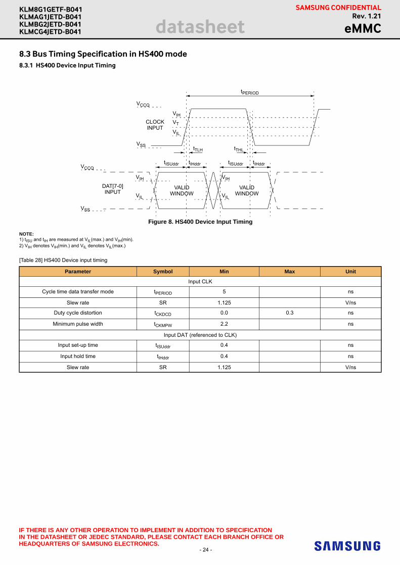
8.3 Bus Timing Specification in HS400 mode8.3.1 HS400 Device Input Timing
Figure 8. HS400 Device Input Timing
NOTE:1) tISU and tIH are measured at VIL(max.) and VIH(min). 2) VIH denotes VIH(min.) and VIL denotes VIL(max.)
[Table 28] HS400 Device input timing
Parameter Symbol Min Max Unit
Input CLK
Cycle time data transfer mode tPERIOD 5 ns
Slew rate SR 1.125 V/ns
Duty cycle distortion tCKDCD 0.0 0.3 ns
Minimum pulse width tCKMPW 2.2 ns
Input DAT (referenced to CLK)
Input set-up time tISUddr 0.4 ns
Input hold time tIHddr 0.4 ns
Slew rate SR 1.125 V/ns
VCCQ
VSS
VSS
VCCQ
DAT[7-0]INPUT
CLOCKINPUT
VALIDWINDOW
VALIDWINDOW
tISUddr tIHddr tISUddr tIHddr
VIL
VIH
VIL
VIH
tTLH tTHL
VIL
VIH
VT
tPERIOD

- 25 -
IF THERE IS ANY OTHER OPERATION TO IMPLEMENT IN ADDITION TO SPECIFICATIONIN THE DATASHEET OR JEDEC STANDARD, PLEASE CONTACT EACH BRANCH OFFICE OR HEADQUARTERS OF SAMSUNG ELECTRONICS.
datasheet eMMCRev. 1.21
SAMSUNG CONFIDENTIALKLM8G1GETF-B041KLMAG1JETD-B041KLMBG2JETD-B041KLMCG4JETD-B041
8.3.2 HS400 Device Output Timing
Data Strobe is used to read data (data read and CRC status response read) in HS400 mode. The device output value of Data Strobe is “High-Z” when the device is not in outputting data (data read, CRC status response). Data Strobe is toggled only during data read period.
Figure 9. HS400 Device Output Timing
NOTE:VOH denotes VOH(min.) and VOL denotes VOL(max.).
HS400 Device Output timing
Parameter Symbol Min Max Unit
Data Strobe
Cycle time data transfer mode tPERIOD 5 ns
Slew rate SR 1.125 V/ns
Duty cycle distortion tDSDCD 0.0 0.2 ns
Minimum pulse width tDSMPW 2.0 ns
Read pre-amble tRPRE 0.4 - tPERIOD
Read post-amble tRPST 0.4 - tPERIOD
Output DAT (referenced to Data Strobe)
Output skew tRQ - 0.4 ns
Output hold skew tRQH - 0.4 ns
Slew rate SR 1.125 V/ns
VCCQ
VSS
VCCQ
VSS
DAT[7-0]OUTPUT
VALIDWINDOW
VALIDWINDOW
VOH
VOL
VOH
VOL
VOH
VT
VOL
tPERIOD
tTLH
tRQ
tTHL
tRQH
Data StrobeOUTPUT

- 26 -
IF THERE IS ANY OTHER OPERATION TO IMPLEMENT IN ADDITION TO SPECIFICATIONIN THE DATASHEET OR JEDEC STANDARD, PLEASE CONTACT EACH BRANCH OFFICE OR HEADQUARTERS OF SAMSUNG ELECTRONICS.
datasheet eMMCRev. 1.21
SAMSUNG CONFIDENTIALKLM8G1GETF-B041KLMAG1JETD-B041KLMBG2JETD-B041KLMCG4JETD-B041
8.4 Bus signal levelsAs the bus can be supplied with a variable supply voltage, all signal levels are related to the supply voltage.
8.4.1 Open-drain mode bus signal level
[Table 29] Open-drain bus signal level
NOTE:1) Because Voh depends on external resistance value (including outside the package), this value does not apply as device specification. Host is responsible to choose the external pull-up and open drain resistance value to meet Voh Min value.
8.4.2 Push-pull mode bus signal level eMMC
The device input and output voltages shall be within the following specified ranges for any VCCQ of the allowed voltage range
[Table 30] Push-pull signal level—high-voltage eMMC
[Table 31] Push-pull signal level—1.70 - 1.95 VCCQ voltage Range
NOTE:1) 0.7*VCCQ for MMC4.3 and older revisions.2) 0.3*VCCQ for MMC4.3 and older revisions.
Parameter Symbol Min Max. Unit Conditions
Output HIGH voltage VOH VDD - 0.2 - V 1)
Output LOW voltage VOL - 0.3 V IOL = 2 mA
Parameter Symbol Min Max. Unit Conditions
Output HIGH voltage VOH 0.75*VDD - V IOH = -100 uA@VCCQ min
Output LOW voltage VOL - 0.125*VDD V IOL = 100 uA@VCCQ min
Input HIGH voltage VIH 0.625*VDD VDD + 0.3 V -
Input LOW voltage VIL VSS - 0.3 0.25*VDD V -
Parameter Symbol Min Max. Unit Conditions
Output HIGH voltage VOH VCCQ - 0.45V - V IOH = -2mA
Output LOW voltage VOL - 0.45V V IOL = 2mA
Input HIGH voltage VIH 0.65*VCCQ 1) VCCQ + 0.3 V -
Input LOW voltage VIL VSS - 0.3 0.35*VCCQ2) V -
V
t
inputhigh level
inputlow level
outputhigh level
outputlow level
undefined
VDD
VIH
VOH
VIL
VSS
VOL
- 27 -
IF THERE IS ANY OTHER OPERATION TO IMPLEMENT IN ADDITION TO SPECIFICATIONIN THE DATASHEET OR JEDEC STANDARD, PLEASE CONTACT EACH BRANCH OFFICE OR HEADQUARTERS OF SAMSUNG ELECTRONICS.
datasheet eMMCRev. 1.21
SAMSUNG CONFIDENTIALKLM8G1GETF-B041KLMAG1JETD-B041KLMBG2JETD-B041KLMCG4JETD-B041
9.0 DC PARAMETER9.1 Active Power Consumption during operation
[Table 32] Active Power Consumption during operation
* Power Measurement conditions: Bus configuration =x8 @HS400* The measurement for max RMS current is the average RMS current consumption over a period of 100ms
9.2 Standby Power Consumption in auto power saving mode and standby state.[Table 33] Standby Power Consumption in auto power saving mode and standby state
NOTE:Power Measurement conditions: Bus configuration =x8, No CLK*Typical value is measured at VCC=3.3V, TA=25°C. Not 100% tested.
9.3 Sleep Power Consumption in Sleep State[Table 34] Sleep Power Consumption in Sleep State
NOTE:Power Measurement conditions: Bus configuration =x8, No CLK1) In auto power saving mode, VCC power can not be turned off. However in sleep mode VCC power can be turned off.
9.4 Supply Voltage
[Table 35] Supply voltage
Density NAND Type VCCQ VCC Unit
8 GB 64Gb x 1
180
50
mA16 GB 128Gb x 1
32 GB 128Gb x 2 100
64 GB 128Gb x 4 200
Density NAND TypeVCCQ VCC
Unit25C(Typ) 85C 25C(Typ) 85C
8 GB 64Gb x 1
120 400
40 85
uA16 GB 128Gb x 1
32 GB 128Gb x 2 50 135
64 GB 128Gb x 4 70 235
Density NAND TypeVCCQ
VCC Unit25C(Typ) 85C
8 GB 64Gb x 1
120 400 01) uA16 GB 128Gb x 1
32 GB 128Gb x 2
64 GB 128Gb x 4
Item Min Max Unit
VCCQ 1.70 1.95 V
VCC 2.7 3.6 V
VSS -0.5 0.5 V

- 28 -
IF THERE IS ANY OTHER OPERATION TO IMPLEMENT IN ADDITION TO SPECIFICATIONIN THE DATASHEET OR JEDEC STANDARD, PLEASE CONTACT EACH BRANCH OFFICE OR HEADQUARTERS OF SAMSUNG ELECTRONICS.
datasheet eMMCRev. 1.21
SAMSUNG CONFIDENTIALKLM8G1GETF-B041KLMAG1JETD-B041KLMBG2JETD-B041KLMCG4JETD-B041
9.5 Bus Signal Line LoadThe total capacitance CL of each line of the eMMC bus is the sum of the bus master capacitance CHOST, the bus capacitance CBUS itself and the capaci-
tance CDEVICE of the eMMC connected to this line:
CL = CHOST + CBUS + CDEVICEThe sum of the host and bus capacitances should be under 20pF.
[Table 36] Bus Signal Line Load
[Table 37] Capacitance and Resistance for HS400 mode
sParameter Symbol Min Typ. Max Unit Remark
Pull-up resistance for CMD RCMD 4.7 100 KOhm to prevent bus floating
Pull-up resistance for DAT0-DAT7 RDAT 10 100 KOhm to prevent bus floating
Internal pull up resistance DAT1-DAT7 Rint 10 150 KOhmto prevent unconnected lines floating
Single Device capacitance CDEVICE 12 pF
Maximum signal line inductance 16 nH fPP <= 52 MHz
Parameter Symbol Min Typ Max Unit Remark
Bus signal line capacitance CL 13 pF Single Device
Single Device capacitance CDEVICE 6 pF
Pull-down resistance for Data Strobe RData Strobe 10 100 KOhm