sam8213b memsdigitaloutputmotionsensor low ...1/32 sam8213b memsdigitaloutputmotionsensor...
TRANSCRIPT

1/ 32 www.sam-elec.cn
SAM8213B
MEMS digital output motion sensor
low-power high performance 3-axes “DSC-XYZ” accelerometer
Key Features Supply voltage, 1.62V to 3.6V
For 2x2x1.1 mm LGA-12 package
User selectable range, ±2g, ±4g, ±8g , ±16g
User selectable data output rate
Digital I2C output interface
14 bit resolution
Product OverviewThe SAM8213B sensor is a low power high performance
Low power consumption
1 Programmable interrupt generators with independent
function for motion detection
Factory programmable offset and sensitivity
RoHS compliant
Applications User interface for mobile phone and PMP
Gesture recognition
Active monitoring
Power management
Vibration monitoring
capacitive three-axis linear accelerometer developed by
micro-machined technology. The device is available in a
2x2x1.1 mm land grid array (LGA) and it is guaranteed to
operate over an extended temperature range from -40°C to
+85°C. The sensor element is fabricated by single crystal
silicon with DRIE process and is protected by hermetically
sealed silicon cap from the environment. The device features
user selectable full scale of ±2g/ ±4g/ ±8g /± 16g
measurement range with data output rate from 1Hz to 1 kHz
with signal condition, active detection imbedded. The
SAM8213B has a power-down mode that makes it good for
handset power management. One independent and flexible
interrupts provided greatly simplify the algorithm for
various motion status detections. Standard I2C interface is
used to communicate with the chip.

2/ 32 www.sam-elec.cn
Content1. Block diagram and pin description................................................................................................................................ 7
1.1. Block diagram...............................................................................................................................................71.2. Pin description.............................................................................................................................................. 7
2. Mechanical and electrical specifications...................................................................................................................... 92.1. Mechanical characteristics............................................................................................................................92.2. Electrical characteristics............................................................................................................................. 102.3. Absolute maximum ratings.........................................................................................................................10
3. Communication interface............................................................................................................................................113.1. Communication interface Electrical specification......................................................................................11
3.1.1. I2C Electrical specification.................................................................................................................113.2. Digital interface operation.......................................................................................................................... 12
3.2.1. I2C Operation..................................................................................................................................... 124. Terminology and functionality................................................................................................................................... 14
4.1. Terminology................................................................................................................................................144.1.1. Sensitivity 144.1.2. Zero-g level14
4.2. Functionality............................................................................................................................................... 144.2.1. Power mode144.2.2. Sensor data 15
4.2.3. Factory calibration.............................................................................................................................. 154.3. Interrupt controller......................................................................................................................................15
4.3.1. General features.................................................................................................................................. 154.3.2. Mapping 16
4.3.3. Electrical behavior (INT to open-drive or push-pull)........................................................................ 164.3.4. New data interrupt.............................................................................................................................. 174.3.5. Active detection.................................................................................................................................. 17
5. Application hints.........................................................................................................................................................186. Register mapping........................................................................................................................................................ 197. Registers description...................................................................................................................................................20
7.1. CONFIG (00H)...........................................................................................................................................207.2. CHIPID (01h)............................................................................................................................................. 207.3. ACC_X_LSB (02H), ACC_X_MSB (03H)............................................................................................... 207.4. ACC_Y_LSB (04H), ACC_Y_MSB (05H)............................................................................................... 217.5. ACC_Z_LSB (06H), ACC_Z_MSB (07H)................................................................................................ 217.6. MOTION_FLAG (09H)............................................................................................................................. 217.7. NEWDATA_FLAG (0AH)......................................................................................................................... 227.8. ACTIVE_STATUS (0BH).......................................................................................................................... 227.9. RANGE (0FH)............................................................................................................................................227.10. ODR_AXIS (10H)...................................................................................................................................... 237.11. MODE_BW (11H)......................................................................................................................................237.12. SWAP_POLARITY (12H)..........................................................................................................................247.13. INT_SET1 (16H)........................................................................................................................................ 24

3/ 32 www.sam-elec.cn
7.14. INT_SET2 (17H)........................................................................................................................................ 257.15. INT_MAP1 (19H)...................................................................................................................................... 257.16. INT_MAP2 (1AH)......................................................................................................................................257.17. INT_CONFIG (20H).................................................................................................................................. 267.18. INT_LATCH (21H).................................................................................................................................... 267.19. ACTIVE_DUR (27H).................................................................................................................................277.20. ACTIVE_THS (28H)..................................................................................................................................27
8. Package information................................................................................................................................................... 288.1. Outline dimensions..................................................................................................................................... 288.2. Landing pattern recommendation...............................................................................................................298.3. Tape and reel specification......................................................................................................................... 30
9. Reliability....................................................................................................................................................................3110. Revision history.......................................................................................................................................................... 32

4/ 32 www.sam-elec.cn
Jan. 2018 Rev 0.2 SAM8213B
List of tablesTable 1.Pin description..................................................................................................................................................8Table 2.Mechanical characteristic.................................................................................................................................9Table 3.Electrical characteristics.................................................................................................................................10Table 4.Absolute maximum ratings............................................................................................................................ 10Table 5.Electrical specification of the I2C interface pins............................................................................................11Table 6.The interface pins........................................................................................................................................... 12Table 7.I2C Address..................................................................................................................................................... 12Table 8.SAD+Read/Write patterns.............................................................................................................................. 12Table 9.Transferwhen master is writing one byte to slave........................................................................................ 13Table 10.Transfer when master is writing multiple bytes to slave..............................................................................13Table 11.Transfer when master is receiving (reading) one byte of data from slave...................................................13Table 12.Transfer when master is receiving (reading) multiple bytes of data from slave..........................................13Table 13.Interrupt mode selection............................................................................................................................. 15Table 14.Register address map...................................................................................................................................19Table 15.CONFIG register............................................................................................................................................20Table 16.CONFIG description......................................................................................................................................20Table 17.CHIPID register............................................................................................................................................. 20Table 18.ACC_X_LSB register...................................................................................................................................... 20Table 19.ACC_X_MSB register.................................................................................................................................... 20Table 20.ACC_Y_LSB register...................................................................................................................................... 21Table 21.ACC_Y_MSB register.....................................................................................................................................21Table 22.ACC_Z_LSB register...................................................................................................................................... 21Table 23.ACC_Z_MSB register.....................................................................................................................................21Table 24.MOTION_FLAG register................................................................................................................................21Table 25.MOTION_FLAG register description.............................................................................................................21Table 26.NEWDATA_FLAG register..............................................................................................................................22Table 27.NEWDATA_FLAG register description..........................................................................................................22Table 28.ACTIVE_STATUS register.............................................................................................................................. 22Table 29.ACTIVE_STATUS register description........................................................................................................... 22Table 30.RANGE register.............................................................................................................................................22Table 31.RANGE register description..........................................................................................................................22Table 32.ODR_AXIS register........................................................................................................................................23Table 33.ODR_AXIS register description.....................................................................................................................23Table 34.MODE_BW register...................................................................................................................................... 23Table 35.MODE_BW register description................................................................................................................... 23Table 36.SWAP_POLARITY register.............................................................................................................................24Table 37.SWAP_POLARITY register description..........................................................................................................24Table 38.INT_SET1 register......................................................................................................................................... 24Table 39.INT_SET1 register description......................................................................................................................24Table 40.INT_SET2 register......................................................................................................................................... 25Table 41.INT_SET2 register description......................................................................................................................25Table 42.INT_MAP1 register....................................................................................................................................... 25

5/ 32 www.sam-elec.cn
Jan. 2018 Rev 0.2 SAM8213B
Table 43.INT_MAP1 register description....................................................................................................................25Table 44.INT_MAP2 register.......................................................................................................................................25Table 45.INT_MAP2 register description....................................................................................................................25Table 46.INT_CONFIG register.................................................................................................................................... 26Table 47.INT_CONFIG register description.................................................................................................................26Table 48.INT_LATCH register...................................................................................................................................... 26Table 49.INT_LATCH register description................................................................................................................... 26Table 50.ACTIVE_DUR register....................................................................................................................................27Table 51.ACTIVE_DUR register description................................................................................................................ 27Table 52.ACTIVE_THS register.....................................................................................................................................27Table 53.ACTIVE_THS register description................................................................................................................. 27Table 54.Accelerated Life Tests................................................................................................................................... 31Table 55.Component Level Tests.................................................................................................................................31Table 56.Document revision history...........................................................................................................................32
6/ 32 www.sam-elec.cn
Jan. 2018 Rev 0.2 SAM8213B
List of figuresFigure 1 Block Diagram............................................................................................................................................. 7Figure 2 Pin description............................................................................................................................................. 7Figure 3 I2C Slave timing diagram.........................................................................................................................11Figure 4 I2C Protocol............................................................................................................................................... 12Figure 5 power mode................................................................................................................................................ 14Figure 6 Interrupt mode.......................................................................................................................................... 16Figure 7 SAM8213B I2C electrical connect........................................................................................................... 18Figure 8 12 Pin LGA Mechanical data andpackage dimensions........................................................................ 28Figure 9 landing patterns; dimensions in mm....................................................................................................... 29Figure 10 Tape and reel dimension in mm............................................................................................................. 30

7/ 32 www.sam-elec.cn
Jan. 2018 Rev 0.2 SAM8213B
1. Block diagram and pin description
1.1.Block diagram
Figure 1 Block Diagram
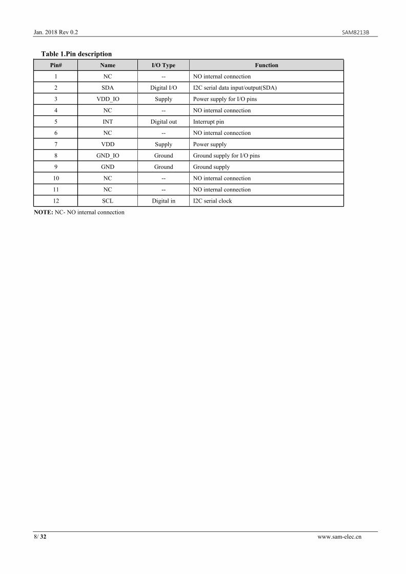
1.2.Pin description
Figure 2 Pin description
8/ 32 www.sam-elec.cn
Jan. 2018 Rev 0.2 SAM8213B
Table 1.Pin descriptionPin# Name I/O Type Function
1 NC -- NO internal connection
2 SDA Digital I/O I2C serial data input/output(SDA)
3 VDD_IO Supply Power supply for I/O pins
4 NC -- NO internal connection
5 INT Digital out Interrupt pin
6 NC -- NO internal connection
7 VDD Supply Power supply
8 GND_IO Ground Ground supply for I/O pins
9 GND Ground Ground supply
10 NC -- NO internal connection
11 NC -- NO internal connection
12 SCL Digital in I2C serial clock
NOTE: NC- NO internal connection

9/ 32 www.sam-elec.cn
Jan. 2018 Rev 0.2 SAM8213B
2. Mechanical and electrical specifications
2.1.Mechanical characteristics
VDD = 2.5 V, T = 25 °C unless otherwise noted.
Table 2.Mechanical characteristicSymbol Parameter Test conditions Min Type Max Unit
FS Measurement range
FS bit set to 00 ±2 g
FS bit set to 01 ±4 g
FS bit set to 10 ±8 g
FS bit set to 11 ±16 g
So Sensitivity
FS bit set to 00 4096 LSB/g
FS bit set to 01 2048 LSB/g
FS bit set to 10 1024 LSB/g
FS bit set to 11 512 LSB/g
TCSo Sensitivity change vs. temperature FS bit set to 00 ±0.01 %/°C
Tyoff Typical zero-g level offset accuracy ±70 mg
Tcoff Zero-g level change vs. temperature Max delta from 25°C ±0.6 mg/°C
Noise XYZ RMS noise
FS bit set to 00,
normal mode,
BW = 100Hz
1.5 mg
Top Operation temperature range -40 85 °C

10/ 32 www.sam-elec.cn
Jan. 2018 Rev 0.2 SAM8213B
2.2.Electrical characteristics
Vdd = 2.5 V, T = 25 °C unless otherwise noted
Table 3.Electrical characteristicsSymbol Parameter Test conditions Min Typ. Max Unit
VDD Supply voltage 1.62 2.5 3.6 V
VDD_IO I/O Pins supply voltage 1.62 VDD V
IDD current consumption in normal modeTop=25℃,
ODR=125Hz95 uA
IDD_SM current consumption in suspend mode Top=25℃ 0.7 uA
TVDD VDD&VDDIO power up time 100 ms
VIH Digital high level input voltage I2C 0.7*Vdd_IO V
VIL Digital low level input voltage I2C 0.3*Vdd_IO V
VOH high level output voltage 0.9*Vdd_IO V
VOL Low level output voltage 0.1*Vdd_IO V
BW System bandwidth 100 500 Hz
ODR Output data rate 1 1000 Hz
TWU Wake-up time From stand-by 1 ms
TSU Start-up time From power off 3 ms
PSRR Power Supply Rejection Rate Top=25℃ 20 mg/V
2.3.Absolute maximum ratings
Stresses below those listed as “absolute maximum ratings” may cause permanent damage to the device. This is a stress rating only and
functional operation of the device under these conditions is not implied. Exposure to maximum rating conditions for extended periods may
affect device reliability.
Table 4.Absolute maximum ratingsParameter Test conditions Min Max Unit
Storage Temperature -45 125 ℃
Supply Voltage VDD Supply pins -0.3 4.25 V
Supply Voltage VDD_IO Logic pins -0.3 Vdd_IO+0.3 V
ESD Rating HMB,R=1.5k,C=100pF ±2 kV
Mechanical Shock Duration<200us 10,000 g
Note: Supply voltage on any pin should never exceed 4.25V
This is a mechanical shock sensitive device, improper handling can cause permanent damages to the part.
This is an ESD sensitive device, improper handling can cause permanent damages to the part.
11/ 32 www.sam-elec.cn
Jan. 2018 Rev 0.2 SAM8213B
3. Communication interface
3.1.Communication interface Electrical specification
3.1.1. I2C Electrical specification
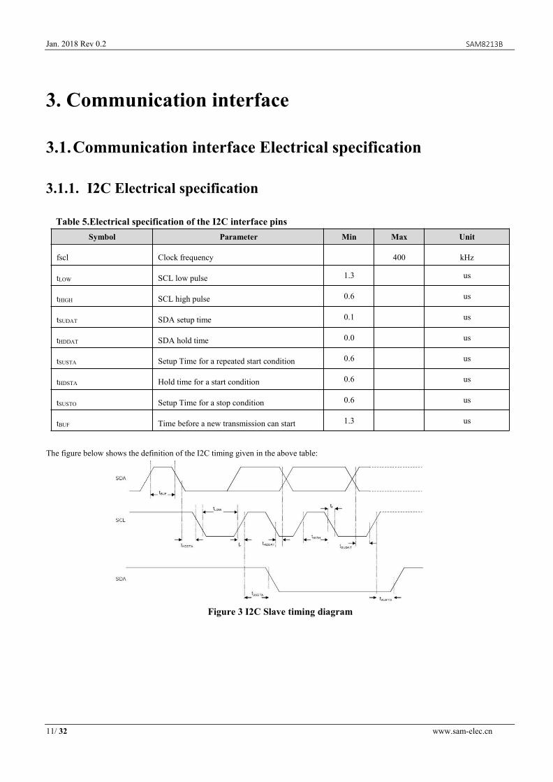
Table 5.Electrical specification of the I2C interface pinsSymbol Parameter Min Max Unit
fscl Clock frequency 400 kHz
tLOW SCL low pulse 1.3 us
tHIGH SCL high pulse 0.6 us
tSUDAT SDA setup time 0.1 us
tHDDAT SDA hold time 0.0 us
tSUSTA Setup Time for a repeated start condition 0.6 us
tHDSTA Hold time for a start condition 0.6 us
tSUSTO Setup Time for a stop condition 0.6 us
tBUF Time before a new transmission can start 1.3 us
The figure below shows the definition of the I2C timing given in the above table:
Figure 3 I2C Slave timing diagram

12/ 32 www.sam-elec.cn
Jan. 2018 Rev 0.2 SAM8213B
3.2.Digital interface operation
The SAM8213B supports the serial digital interface protocols for communications as slave with a host device: I2C. The interface pin is
given in the following table:
Table 6.The interface pinsPIN name I2C
SCL Serial clock
SDA Serial Data
3.2.1.I2C Operation
I2C bus uses SCL and SDA as signal lines. Both lines are connected to VDDIO externally via pull-up resistors so that they are pulled high
when the bus is free. The I2C device address of SAM8213B is shown below.
Table 7.I2C AddressSAD6 SAD5 SAD4 SAD3 SAD2 SAD1 SAD0 W/R
0 1 0 0 1 1 1 0/1
Table 8.SAD+Read/Write patternsCommand SAD[6:0] R/W SAD+R/W
Read 0100111(27h) 1 01001111(4fh)
Write 0100111(27h) 0 01001110(4eh)
The I2C interface protocol has special bus signal conditions. Start (S), stop (P) and binary data conditions are shown below. At start
condition, SCL is high and SDA has a falling edge. Then the slave address is sent. After the 7 address bits, the direction control bit R/W
selects the read or write operation. When a slave device recognizes that it is being addressed, it should acknowledge by pulling SDA low in
the ninth SCL (ACK) cycle.
At stop condition, SCL is also high, but SDA has a rising edge. Data must be held stable at SDA when SCL is high. Data can change value
at SDA only when SCL is low.
Figure 4 I2C Protocol
13/ 32 www.sam-elec.cn
Jan. 2018 Rev 0.2 SAM8213B
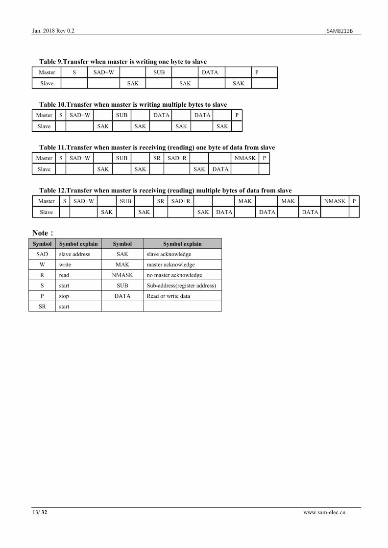
Table 9.Transfer when master is writing one byte to slaveMaster S SAD+W SUB DATA P
Slave SAK SAK SAK
Table 10.Transfer when master is writing multiple bytes to slaveMaster S SAD+W SUB DATA DATA P
Slave SAK SAK SAK SAK
Table 11.Transfer when master is receiving (reading) one byte of data from slaveMaster S SAD+W SUB SR SAD+R NMASK P
Slave SAK SAK SAK DATA
Table 12.Transfer when master is receiving (reading) multiple bytes of data from slaveMaster S SAD+W SUB SR SAD+R MAK MAK NMASK P
Slave SAK SAK SAK DATA DATA DATA
Note:Symbol Symbol explain Symbol Symbol explain
SAD slave address SAK slave acknowledge
W write MAK master acknowledge
R read NMASK no master acknowledge
S start SUB Sub-address(register address)
P stop DATA Read or write data
SR start

14/ 32 www.sam-elec.cn
Jan. 2018 Rev 0.2 SAM8213B
4. Terminology and functionality
4.1.Terminology
4.1.1.Sensitivity
Sensitivity describes the gain of the sensor and can be determined e.g. by applying 1 g acceleration to it. As the sensor can measure DC
accelerations this can be done easily by pointing the axis of interest towards the center of the earth, noting the output value, rotating the
sensor by 180 degrees (pointing to the sky) and noting the output value again. By doing so, ±1 g acceleration is applied to the sensor.
Subtract the larger output value from the smaller one, and dividing the result by 2, leads to the actual sensitivity of the sensor. This value
changes very little over temperature and also time. The sensitivity tolerance describes the range of sensitivities of a large population of
sensors.
4.1.2.Zero-g level
Zero-g level offset (TyOff) describes the deviation of an actual output signal from the ideal output signal if no acceleration is present. A
sensor in a steady state on a horizontal surface measure 0 g in X axis and 0 g in Y axis whereas the Z axis measure 1 g. The output is
ideally in the middle of the dynamic range of the sensor (content of output data registers are 00h, data expressed as 2’s complement
number). A deviation from ideal value in this case is called Zero-g offset. Offset is to some extent a result of stress to MEMS sensor and
therefore the offset can slightly change after mounting the sensor onto a printed circuit board or exposing it to extensive mechanical stress.
Offset changes little over temperature; see “Zero-g level change vs. temperature”. The Zero-g level tolerance (TyOff) describes the
standard deviation of the range of Zero-g levels of a population of sensors.
4.2.Functionality
4.2.1.Power mode
The SAM8213B has two different power modes: normal and suspend mode.
Figure 5 power modeIn the normal mode, the device is periodically switching between a sleep phase and a wake-up phase. The wake-up phase essentially
corresponding to operation in measure state with complete power-up of the circuitry at the current setting ODR when “autosleep_en”bit of
“MODE_BW” (11H) register is set to 0, but “autosleep_en”bit is set to 1, the measure state works at 12.5hz in inactive state and auto

15/ 32 www.sam-elec.cn
Jan. 2018 Rev 0.2 SAM8213B
switched to operation mode during active state. During the sleep phase the analog part except the oscillator is powered down.
During the wake-up phase, if an enabled interrupt is detected, the device stays in the wake-up phase as long as the interrupt condition
endures (non-latched interrupt), or until the latch time expires (temporary latched interrupt), or until the interrupt is reset (latched interrupt).
If no interrupt detected, the device enters the sleep phase.
Suspend mode: power-down mode.
4.2.2.Sensor data
The width of acceleration data is 14bits given in two’s complement representation. The 14bits for each axis are split into an MSB part (one
byte containing bits 13 to 6) and an LSB lower part (one byte containing bits 5 to 0).
4.2.3.Factory calibration
The IC is factory calibrated for sensitivity (So) and Zero-g level (TyOff). The trimming values are stored inside the chip’s nonvolatile
memory. The trimming parameters are loaded to registers while SAM8213B reset (POR or software reset). This allows using the device
without further calibration.
4.3.Interrupt controller
Interrupt engines are integrated in the SAM8213B. Each interrupt can be independently enabled and configured. If the condition of an
enabled interrupt is fulfilled, the corresponding status bit is set to 1 and the interrupt pin is activated. The pin state is a logic ‘or’
combination of all mapped interrupts to the interrupt pin.
4.3.1.General features
An interrupt is cleared depending on the selected interrupt mode, which is common to all interrupts. There are three different interrupt
modes: non-latched, latched and temporary. The mode is selected by the ‘latch_int’ bits according to the following table.
Table 13.Interrupt mode selectionlatch_INT Interrupt mode
0000 non-latched
0001 temporary latched 250ms
0010 temporary latched 500ms
0011 temporary latched 1s
0100 temporary latched 2s
0101 temporary latched 4s
0110 temporary latched 8s
0111 latched
1000 non-latched
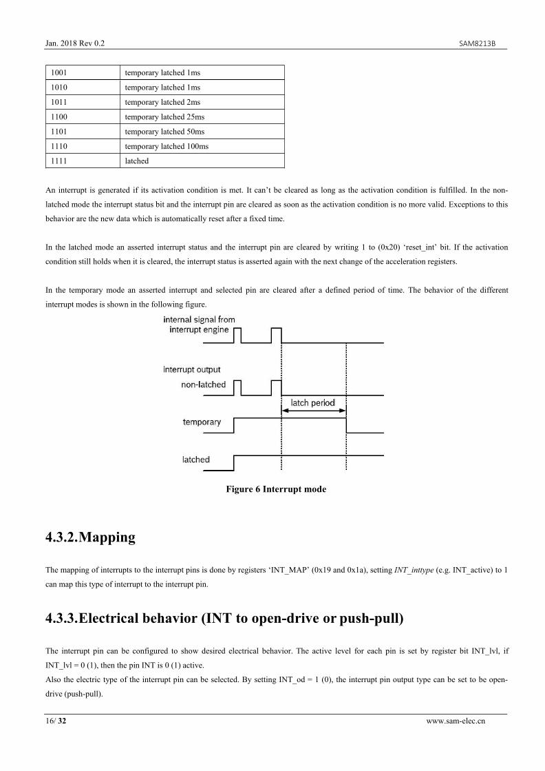
16/ 32 www.sam-elec.cn
Jan. 2018 Rev 0.2 SAM8213B
1001 temporary latched 1ms
1010 temporary latched 1ms
1011 temporary latched 2ms
1100 temporary latched 25ms
1101 temporary latched 50ms
1110 temporary latched 100ms
1111 latched
An interrupt is generated if its activation condition is met. It can’t be cleared as long as the activation condition is fulfilled. In the non-
latched mode the interrupt status bit and the interrupt pin are cleared as soon as the activation condition is no more valid. Exceptions to this
behavior are the new data which is automatically reset after a fixed time.
In the latched mode an asserted interrupt status and the interrupt pin are cleared by writing 1 to (0x20) ‘reset_int’ bit. If the activation
condition still holds when it is cleared, the interrupt status is asserted again with the next change of the acceleration registers.
In the temporary mode an asserted interrupt and selected pin are cleared after a defined period of time. The behavior of the different
interrupt modes is shown in the following figure.
Figure 6 Interrupt mode
4.3.2.Mapping
The mapping of interrupts to the interrupt pins is done by registers ‘INT_MAP’ (0x19 and 0x1a), setting INT_inttype (e.g. INT_active) to 1
can map this type of interrupt to the interrupt pin.
4.3.3.Electrical behavior (INT to open-drive or push-pull)
The interrupt pin can be configured to show desired electrical behavior. The active level for each pin is set by register bit INT_lvl, if
INT_lvl = 0 (1), then the pin INT is 0 (1) active.
Also the electric type of the interrupt pin can be selected. By setting INT_od = 1 (0), the interrupt pin output type can be set to be open-
drive (push-pull).
17/ 32 www.sam-elec.cn
Jan. 2018 Rev 0.2 SAM8213B
4.3.4.New data interrupt
This interrupt serves for synchronous reading of acceleration data. It is generated after an acceleration data was calculated. The interrupt is
cleared automatically before the next acceleration data is ready.
4.3.5.Active detection
Active detection uses the slope between successive acceleration signals to detect changes in motion. An interrupt is generated when the
slope (absolute value of acceleration difference) exceeds a preset threshold. The threshold is set with the value of 28H register with the
LSB corresponding to 255LSB of acceleration data that is 3.9mg in 2g-range, 7.8mg in 4g-range, 15.6mg in 8g-range and 31.3mg in 16g-
range. And the maximum value is 1g in 2g-range, 2g in 4g-range, 4g in 8g-range and 8g in 16g-range.
The time difference between the successive acceleration signals depends is fixed to 1ms.
Active detection can be enabled (disabled) for each axis separately by writing ‘1’ to bits ‘active_int_en_x/y/z’. The active interrupt is
generated if the slope of any of the enabled axes exceeds the threshold for [‘active_dur’+1] consecutive times. As soon as the slopes of all
enabled axes fall below this threshold for [‘active_dur’+1] consecutive times, the interrupt is cleared unless the interrupt signal is latched.
The interrupt status is stored in the (0x09) ‘active_int’ bit. The (0x0b) bit ‘active_first_x/y/z’ records which axis triggered the active
interrupt first and the sign of this acceleration data that triggered the interrupt is recorded in the (0x0b) bit ‘active_sign’.

18/ 32 www.sam-elec.cn
Jan. 2018 Rev 0.2 SAM8213B
5. Application hints
Figure 7 SAM8213B I2C electrical connectThe device core is supplied through VDD line while the I/O pads are supplied through VDD_IO line. Power supply decoupling capacitors
(100 nF ceramic) should be placed as near as possible to the pin 7 and pin 3 of the device (common design practice).
The functionality of the device and the measured acceleration data is selectable and accessible through the I2C.The functions, the threshold
and the timing of the interrupt pin (INT) can be completely programmed by the user through the I2C interface.
19/ 32 www.sam-elec.cn
Jan. 2018 Rev 0.2 SAM8213B
6. Register mapping
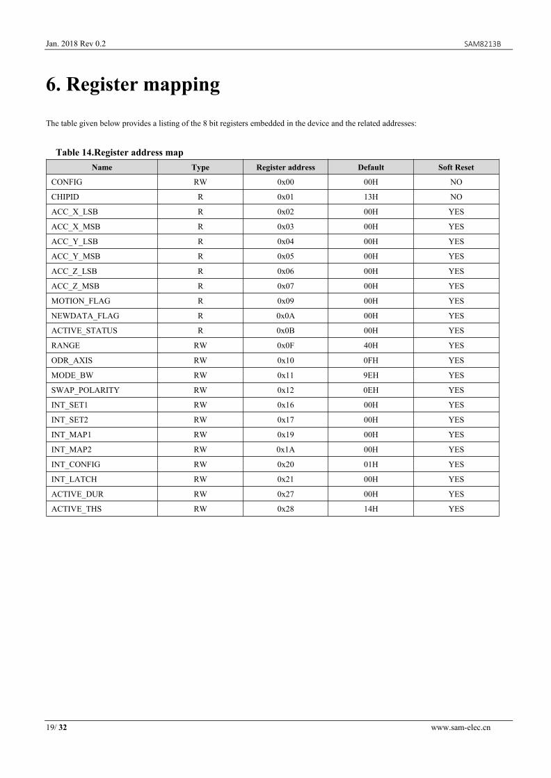
The table given below provides a listing of the 8 bit registers embedded in the device and the related addresses:
Table 14.Register address mapName Type Register address Default Soft Reset
CONFIG RW 0x00 00H NO
CHIPID R 0x01 13H NO
ACC_X_LSB R 0x02 00H YES
ACC_X_MSB R 0x03 00H YES
ACC_Y_LSB R 0x04 00H YES
ACC_Y_MSB R 0x05 00H YES
ACC_Z_LSB R 0x06 00H YES
ACC_Z_MSB R 0x07 00H YES
MOTION_FLAG R 0x09 00H YES
NEWDATA_FLAG R 0x0A 00H YES
ACTIVE_STATUS R 0x0B 00H YES
RANGE RW 0x0F 40H YES
ODR_AXIS RW 0x10 0FH YES
MODE_BW RW 0x11 9EH YES
SWAP_POLARITY RW 0x12 0EH YES
INT_SET1 RW 0x16 00H YES
INT_SET2 RW 0x17 00H YES
INT_MAP1 RW 0x19 00H YES
INT_MAP2 RW 0x1A 00H YES
INT_CONFIG RW 0x20 01H YES
INT_LATCH RW 0x21 00H YES
ACTIVE_DUR RW 0x27 00H YES
ACTIVE_THS RW 0x28 14H YES

20/ 32 www.sam-elec.cn
Jan. 2018 Rev 0.2 SAM8213B
7. Registers description
7.1.CONFIG (00H)
Table 15.CONFIG registerDefault data: 0x00 Type: RW
unused unused Soft Reset unused unused Soft Reset unused unused
Table 16.CONFIG descriptionSoft Reset 1: soft reset
7.2.CHIPID (01h)
Table 17.CHIPID registerDefault data: 0x13 Type: R
0 0 0 1 0 0 1 1
7.3.ACC_X_LSB (02H), ACC_X_MSB (03H)
X-axis acceleration data, the value is expressed in two complement byte and are left justified.
Table 18.ACC_X_LSB registerDefault data: 0x00 Type: R
D[5] D[4] D[3] D[2] D[1] D[0] unused unused
Table 19.ACC_X_MSB registerDefault data: 0x00 Type: R
D[13] D[12] D[11] D[10] D[9] D[8] D[7] D[6]
21/ 32 www.sam-elec.cn
Jan. 2018 Rev 0.2 SAM8213B
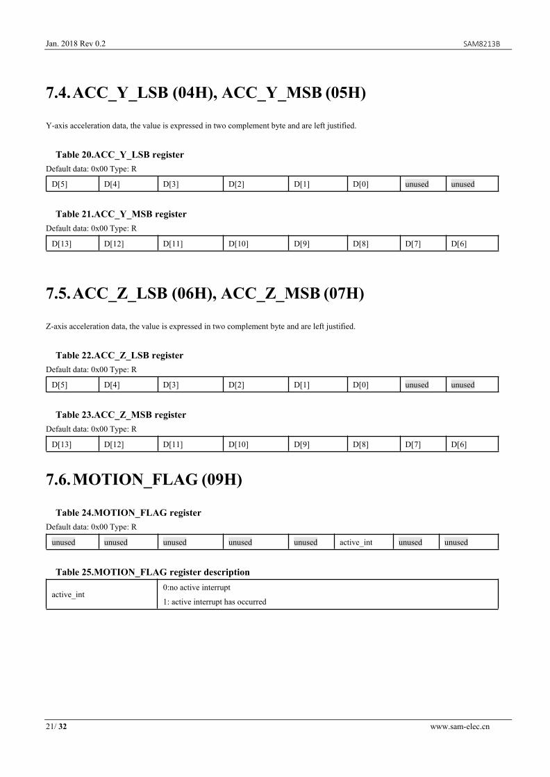
7.4.ACC_Y_LSB (04H), ACC_Y_MSB (05H)
Y-axis acceleration data, the value is expressed in two complement byte and are left justified.
Table 20.ACC_Y_LSB registerDefault data: 0x00 Type: R
D[5] D[4] D[3] D[2] D[1] D[0] unused unused
Table 21.ACC_Y_MSB registerDefault data: 0x00 Type: R
D[13] D[12] D[11] D[10] D[9] D[8] D[7] D[6]
7.5.ACC_Z_LSB (06H), ACC_Z_MSB (07H)
Z-axis acceleration data, the value is expressed in two complement byte and are left justified.
Table 22.ACC_Z_LSB registerDefault data: 0x00 Type: R
D[5] D[4] D[3] D[2] D[1] D[0] unused unused
Table 23.ACC_Z_MSB registerDefault data: 0x00 Type: R
D[13] D[12] D[11] D[10] D[9] D[8] D[7] D[6]
7.6.MOTION_FLAG (09H)
Table 24.MOTION_FLAG registerDefault data: 0x00 Type: R
unused unused unused unused unused active_int unused unused
Table 25.MOTION_FLAG register description
active_int0:no active interrupt
1: active interrupt has occurred
22/ 32 www.sam-elec.cn
Jan. 2018 Rev 0.2 SAM8213B
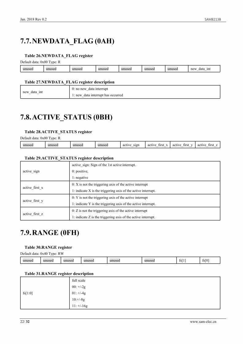
7.7.NEWDATA_FLAG (0AH)
Table 26.NEWDATA_FLAG registerDefault data: 0x00 Type: R
unused unused unused unused unused unused unused new_data_int
Table 27.NEWDATA_FLAG register description
new_data_int0: no new_data interrupt
1: new_data interrupt has occurred
7.8.ACTIVE_STATUS (0BH)
Table 28.ACTIVE_STATUS registerDefault data: 0x00 Type: R
unused unused unused unused active_sign active_first_x active_first_y active_first_z
Table 29.ACTIVE_STATUS register description
active_sign
active_sign: Sign of the 1st active interrupt.
0: positive,
1: negative
active_first_x0: X is not the triggering axis of the active interrupt
1: indicate X is the triggering axis of the active interrupt.
active_first_y0: Y is not the triggering axis of the active interrupt
1: indicate Y is the triggering axis of the active interrupt.
active_first_z0: Z is not the triggering axis of the active interrupt
1: indicate Z is the triggering axis of the active interrupt.
7.9.RANGE (0FH)
Table 30.RANGE registerDefault data: 0x40 Type: RW
unused unused unused unused unused unused fs[1] fs[0]
Table 31.RANGE register description
fs[1:0]
full scale
00: +/-2g
01: +/-4g
10:+/-8g
11: +/-16g

23/ 32 www.sam-elec.cn
Jan. 2018 Rev 0.2 SAM8213B
7.10. ODR_AXIS (10H)
Table 32.ODR_AXIS registerDefault data: 0x0F Type: RW
unused unused unused unused ODR[3] ODR[2] ODR[1] ODR[0]
Table 33.ODR_AXIS register description
ODR[3:0]
0000: 1Hz
0001: 1.95Hz
0010: 3.9Hz
0011: 7.81Hz
0100: 15.63Hz
0101: 31.25Hz
0110: 62.5Hz
0111: 125Hz
1000: 250Hz
1001: 500Hz
1010-1111: 1000Hz
7.11. MODE_BW (11H)
Table 34.MODE_BW registerDefault data: 0x9E Type: RW
PWR_OFF unused unused unused unused BW[1] BW[0] autosleep_en
Table 35.MODE_BW register description
PWR_OFF0: normal mode
1: suspend mode
BW[1:0]
Bandwidth
00/11:500hz
01:250
10:100
autosleep_en0: working the current ODR state all the way
1: Working at 12.5hz in inactive state, automatic switched to normal mode during active state

24/ 32 www.sam-elec.cn
Jan. 2018 Rev 0.2 SAM8213B
7.12. SWAP_POLARITY (12H)
Table 36.SWAP_POLARITY registerDefault data: 0x0E Type: RW
Swap & Polarity register is OTP register too, OTP address:0x13
unused unused unused unused X_polarity Y_polarity Z_polarity X_Y_swap
Table 37.SWAP_POLARITY register description
X_polarity0: remain the polarity of X-axis.
1: reverse the polarity of X-axis.
Y_polarity0: remain the polarity of Y-axis.
1: reverse the polarity of Y-axis.
Z_polarity0: remain the polarity of Z-axis.
1: reverse the polarity of Z-axis.
X_Y_swap0: Don’t need swap the output data for X/Y axis
1: swap the output data for X/Y axis.
7.13. INT_SET1 (16H)
Table 38.INT_SET1 registerDefault data: 0x00 Type: RW
INT_source unused unused unused unused active_int_en_z active_int_en_y active_int_en_x
Table 39.INT_SET1 register description
INT_source0:unfiltered data
1:filtered data(ODR)
active_int_en_z0: disable the active interrupt for the z axis.
1: enable the active interrupt for the z axis.
active_int_en_y0: disable the active interrupt for the y axis.
1: enable the active interrupt for the y axis.
active_int_en_x0: disable the active interrupt for the x axis.
1: enable the active interrupt for the x axis.

25/ 32 www.sam-elec.cn
Jan. 2018 Rev 0.2 SAM8213B
7.14. INT_SET2 (17H)
Table 40.INT_SET2 registerDefault data: 0x00 Type: RW
unused unused unused new_data_int_en unused unused unused unused
Table 41.INT_SET2 register description
new_data_int_en0: disable the new data interrupt.
1: enable the new data interrupt.
7.15. INT_MAP1 (19H)
Table 42.INT_MAP1 registerDefault data: 0x00 Type: RW
unused unused unused unused unused INT_active unused unused
Table 43.INT_MAP1 register description
INT_active0: doesn’t mapping active interrupt to INT
1: mapping active interrupt to INT
7.16. INT_MAP2 (1AH)
Table 44.INT_MAP2 registerDefault data: 0x00 Type: RW
unused unused unused unused unused unused unused unused INT_new_data
Table 45.INT_MAP2 register description
INT_new_data0: doesn’t mapping new data interrupt to INT
1: mapping new data interrupt to INT

26/ 32 www.sam-elec.cn
Jan. 2018 Rev 0.2 SAM8213B
7.17. INT_CONFIG (20H)
Table 46.INT_CONFIG registerDefault data: 0x01 Type: RW
Reset_int unused unused unused unused unused INT_od INT_lvl
Table 47.INT_CONFIG register descriptionReset_int Write’1’to reset all latched int.
INT_od0: select push-pull output for INT
1: selects OD output for INT
INT_lvl0: selects active level low for pin INT
1: selects active level high for pin INT
7.18. INT_LATCH (21H)
Table 48.INT_LATCH registerDefault data: 0x00 Type: RW
unused unused unused unused latch_INT[3] latch_INT[2] latch_INT[1] latch_INT[0]
Table 49.INT_LATCH register description
latch_INT[3:0]
0000: non-latched
0001: temporary latched 250ms
0010: temporary latched 500ms
0011: temporary latched 1s
0100: temporary latched 2s
0101: temporary latched 4s
0110: temporary latched 8s
0111: latched
1000: non-latched
1001: temporary latched 1ms
1010: temporary latched 1ms
1011: temporary latched 2ms
1100: temporary latched 25ms
1101: temporary latched 50ms
1110: temporary latched 100ms
1111: latched
27/ 32 www.sam-elec.cn
Jan. 2018 Rev 0.2 SAM8213B
7.19. ACTIVE_DUR (27H)
Table 50.ACTIVE_DUR registerDefault data: 0x00 Type: RW
inactive_dur[3] inactive_dur[2] inactive_dur[1] inactive_dur[0] active_dur[3] active_dur[2] active_dur[1] active_dur[0]
Table 51.ACTIVE_DUR register descriptioninactive_dur[4:0] inactive duration time = (inactive_dur + 1)* ODR_period
active_dur[4:0] active duration time = (active_dur + 1)* ODR_period
7.20. ACTIVE_THS (28H)
Table 52.ACTIVE_THS registerDefault data: 0x14 Type: RW
active_th[7] active_th [6] active_th [5] active_th[4] active_th [3] active_th [2] active_th [1] active_th [0]
Table 53.ACTIVE_THS register description
active_th[7:0]
Threshold of active interrupt=active_th*K(mg)
K = 3.91(2g range),
K = 7.81(4g range),
K = 15.625(8g range),
K = 31.25(16g range)

28/ 32 www.sam-elec.cn
Jan. 2018 Rev 0.2 SAM8213B
8. Package information
8.1.Outline dimensions
The sensor housing is a standard LGA package. Its dimensions are the following:
Figure 8 12 Pin LGA Mechanical data and package dimensions
)(( )

29/ 32 www.sam-elec.cn
Jan. 2018 Rev 0.2 SAM8213B
8.2.Landing pattern recommendation
For the design of the landing patterns, we recommend the following dimensioning:
Figure 9 landing patterns; dimensions in mm

30/ 32 www.sam-elec.cn
Jan. 2018 Rev 0.2 SAM8213B
8.3.Tape and reel specification
The SAM8213B is shipped in a standard pizza box
The box dimension for 1 reel is: L x W x H = 35cm x 35cm x 5cm
SAM8213B quantity: 5000pcs per reel, please handle with care.
Figure 10 Tape and reel dimension in mm
31/ 32 www.sam-elec.cn
Jan. 2018 Rev 0.2 SAM8213B
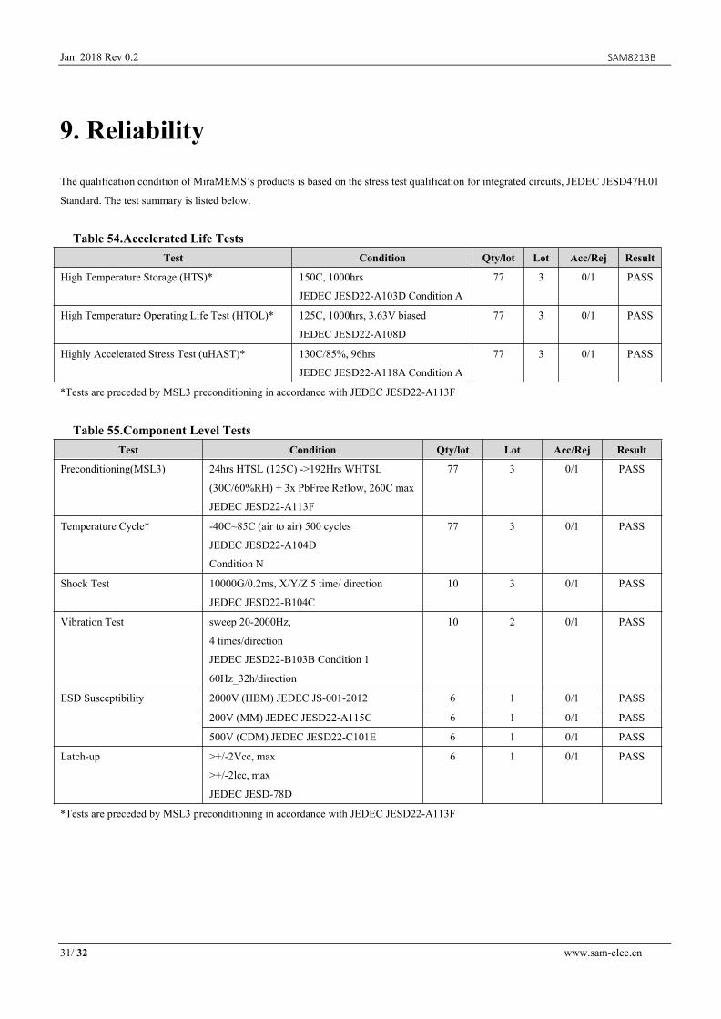
9. Reliability
The qualification condition of MiraMEMS’s products is based on the stress test qualification for integrated circuits, JEDEC JESD47H.01
Standard. The test summary is listed below.
Table 54.Accelerated Life TestsTest Condition Qty/lot Lot Acc/Rej Result
High Temperature Storage (HTS)* 150C, 1000hrs
JEDEC JESD22-A103D Condition A
77 3 0/1 PASS
High Temperature Operating Life Test (HTOL)* 125C, 1000hrs, 3.63V biased
JEDEC JESD22-A108D
77 3 0/1 PASS
Highly Accelerated Stress Test (uHAST)* 130C/85%, 96hrs
JEDEC JESD22-A118A Condition A
77 3 0/1 PASS
*Tests are preceded by MSL3 preconditioning in accordance with JEDEC JESD22-A113F
Table 55.Component Level TestsTest Condition Qty/lot Lot Acc/Rej Result
Preconditioning(MSL3) 24hrs HTSL (125C) ->192Hrs WHTSL
(30C/60%RH) + 3x PbFree Reflow, 260C max
JEDEC JESD22-A113F
77 3 0/1 PASS
Temperature Cycle* -40C~85C (air to air) 500 cycles
JEDEC JESD22-A104D
Condition N
77 3 0/1 PASS
Shock Test 10000G/0.2ms, X/Y/Z 5 time/ direction
JEDEC JESD22-B104C
10 3 0/1 PASS
Vibration Test sweep 20-2000Hz,
4 times/direction
JEDEC JESD22-B103B Condition 1
60Hz_32h/direction
10 2 0/1 PASS
ESD Susceptibility 2000V (HBM) JEDEC JS-001-2012 6 1 0/1 PASS
200V (MM) JEDEC JESD22-A115C 6 1 0/1 PASS
500V (CDM) JEDEC JESD22-C101E 6 1 0/1 PASS
Latch-up >+/-2Vcc, max
>+/-2lcc, max
JEDEC JESD-78D
6 1 0/1 PASS
*Tests are preceded by MSL3 preconditioning in accordance with JEDEC JESD22-A113F
32/ 32 www.sam-elec.cn
Jan. 2018 Rev 0.2 SAM8213B
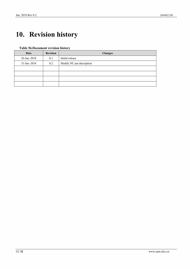
10. Revision history
Table 56.Document revision historyDate Revision Changes
26-Jan.-2018 0.1 Initial release
31-Jan.-2018 0.2 Modify NC pin description