safe fpga design practices for instrumentation and control...
TRANSCRIPT
11
Safe FPGA Design Practices Safe FPGA Design Practices for Instrumentation and for Instrumentation and
Control in Nuclear PlantsControl in Nuclear Plants
Miljko BobrekMiljko Bobrek11, Richard T. Wood, Richard T. Wood11, Christina D. Ward, Christina D. Ward11, Stephen M. Killough, Stephen M. Killough11,,Don BouldinDon Bouldin22, Michael E. Waterman, Michael E. Waterman33
1 Oak Ridge National Laboratory, Oak Ridge, TN1 Oak Ridge National Laboratory, Oak Ridge, TN2 The University of Tennessee, ECE Department, Knoxville, TN2 The University of Tennessee, ECE Department, Knoxville, TN
3 Nuclear Regulatory Commission, Washington, DC3 Nuclear Regulatory Commission, Washington, DC
22
♣ Problem Statement♣ Introduction to FPGAs♣ Safe design practices♣ Validation and Verification♣ Maintainability and Obsolescence♣ Conclusions
Presentation ContentsPresentation Contents

33
♣ Obsolete I&C systems in NP need to be replaced♣ New plants are built that need modern I&C systems♣ Modern, general purpose I&C systems are based on microprocessors,
digital signal processors, microcontrollers, and FPGAs♣ Currently used I&C systems in NP are based on analog electronics,
low-level integration digital circuits, and microcontrollers many ofwhich are obsolete.
♣ NRC needs guidance and acceptance criteria to help with licensing of FPGA-based safety-critical I&C systems in NP
♣ There is no ready-to-use regulatory document for FPGA-based safety systems
Problem StatementProblem Statement

44
♣ Field Programmable Gate Array♣ One of programmable logic devices such as GPP, mC, DSP, and
ASIC.♣ Contains unconnected basic logic elements such as AND gates,
OR gates, and flip-flops.♣ More complex FPGAs include adders, multipliers, memory
blocks, and microprocessors.♣ Interconnections are done by a designer using EDA tools.♣ Some FPGAs can be reconfigured completely or partially during
the development phase or during the exploitation phase♣ FPGAs represent a higher level of integration of digital
hardware, but they also involve software design.
Introduction to Introduction to FPGAsFPGAs
What is an FPGA?What is an FPGA?

55
♣ PROMs in 1950s♣ PLAs in early 1970s♣ PALs in late 1970s♣ GALs in 1980s♣ CPLDs in late 1970s♣ FPGAs in late 1970s♣ Platform FPGAs in late1990s
FPGA HistoryFPGA History
Introduction to Introduction to FPGAsFPGAs

66
Source: Source: AlteraAltera
Introduction to Introduction to FPGAsFPGAs

77
CPLD StructureCPLD Structure
Source: Xilinx Source: Xilinx
Introduction to Introduction to FPGAsFPGAs

88
FPGA StructureFPGA Structure
Source: Source: ActelActel
Introduction to Introduction to FPGAsFPGAs

99
FPGA ClassificationsFPGA Classifications
♣♣ By sizeBy size♣♣ From several thousands to several millions of gatesFrom several thousands to several millions of gates
♣♣ By packagingBy packaging♣♣ Quad Flat Pack, Ball Grid ArrayQuad Flat Pack, Ball Grid Array
♣♣ By configurationBy configuration♣♣ SRAM, EEPROM, FLASH, SRAM, EEPROM, FLASH, One_TimeOne_Time
♣♣ By applicationBy application♣♣ General purpose, High speed, Large designs, Low power, General purpose, High speed, Large designs, Low power, RadRad hardhard
♣♣ By manufacturerBy manufacturer♣♣ ActelActel, , AeroflexAeroflex, , AlteraAltera, Atmel, Cypress, Lattice, , Atmel, Cypress, Lattice, QuicklogicQuicklogic, Xilinx, Xilinx
Introduction to Introduction to FPGAsFPGAs

1010
FPGA Design FPGA Design MethodologyMethodology
Design entryBehavioral SimulationSynthesisPost Synthesis SimulationPlace and RoutePost P&R SimulationFPGA ConfigurationHardware Verification
Source: Source: ActelActel

1111
FPGA Design EntryFPGA Design Entry
process(SCLK,RSTB,NCS)
beginif RSTB = '0' or NCS = '1' then
BIT_CNT <= "0000";elsif SCLK'event and SCLK = '1' then
if BIT_CNT <= "1001" thenBIT_CNT <= BIT_CNT + '1';
elseBIT_CNT <= BIT_CNT;
end if;end if;
end process;
Introduction to Introduction to FPGAsFPGAs

1212
FPGA Design EntryFPGA Design Entry
Introduction to Introduction to FPGAsFPGAs

1313
FPGA Design SimulationFPGA Design Simulation
Introduction to Introduction to FPGAsFPGAs

1414
♣ System Level Design Practices.
♣ Board Level Design Practices.
♣ FPGA Level Design Practices.
Safe FPGA Design PracticesSafe FPGA Design Practices

1515
♣ Design partitioning to FPGAs, DSPs, GPPs, memories, interfaces.
♣ Implementing multiple functions in a single FPGA.
♣ Mixing safety-critical and safety-noncritical designs into a single FPGA
♣ FPGA type and/or size selection.
♣ System partitioning with respect to Validation and Verification
SystemSystem--Level Design PracticesLevel Design Practices

1616
♣ Supply power fluctuations and ground bounce.
♣ Proper power and ground plane design and PCB layer stacking
♣ Selection and proper design of power regulators to satisfy maximum rise-time and power sequencing required for the FPGA power-up
♣ Placement of power decoupling capacitors
♣ Mitigation of Simultaneous Switching Outputs (SSO) effects.
♣ Reducing the output rise time of the FPGA I/Os
BoardBoard--Level Design PracticesLevel Design Practices

1717
♣ Separation of digital and analog parts of the design residing onthe same board
♣ Proper termination and isolation of clock and other high-speed lines
♣ FPGA power dissipation and cooling
♣ Mitigation of whisker growth in lead-free solder
BoardBoard--Level Design PracticesLevel Design Practices

1818
Synchronous vs. asynchronous design
FPGAFPGA--Level Design PracticesLevel Design Practices
Asynchronous/Combinatorial ♣ Faster response, smaller design♣ Prone to glitches, bus skews, timing
issues
Synchronous/Sequential ♣ Slower but controlled response, larger
design♣ Eliminates glitches, bus skews, timing
issues

1919
Metastability
FPGAFPGA--Level Design PracticesLevel Design Practices
Source: Xilinx Source: Xilinx

2020
Global Routing Lines
FPGAFPGA--Level Design PracticesLevel Design Practices

2121
Global Routing Lines
FPGAFPGA--Level Design PracticesLevel Design Practices
Source: Xilinx Source: Xilinx

2222
FPGA Reset
FPGAFPGA--Level Design PracticesLevel Design Practices

2323
Timing constraints
FPGAFPGA--Level Design PracticesLevel Design Practices

2424
FPGAFPGA--Level Design PracticesLevel Design Practices
process(CLK,RST)
beginif RST = '0' or NCS = '1' then
STATE <= "00";OUTPUT <= "00";
elsif CLK'event and CLK = '1' thenif STATE = "00" then
if INPUT <= "00" thenOUTPUT <= "00";STATE <= "00";
elseOUTPUT <= "01";STATE <= "01";
end if;elsif STATE = "01" then
if INPUT <= “10" thenOUTPUT <= "01";STATE <= "01";
elseOUTPUT <= “10";STATE <= “10";
end if;
HDL State Machine Design
elsif STATE = “10" thenif INPUT <= “11" then
OUTPUT <= “10";STATE <= "00";
elseOUTPUT <= "00";STATE <= “10";
end if;=======================
end if;end process;
elseOUTPUT <= “00";STATE <= "00";

2525
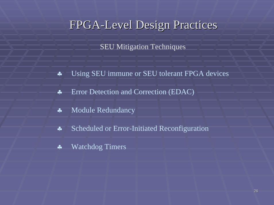
FPGAFPGA--Level Design PracticesLevel Design PracticesSingle Event Upsets (SEU)
Neutron flux as a function of Altitude and LatitudeNeutron flux as a function of Altitude and Latitude
Number of SEU/day in a 1M gate SRAM FPGANumber of SEU/day in a 1M gate SRAM FPGASource: Source: ActelActel
2626
FPGAFPGA--Level Design PracticesLevel Design Practices
SEU Mitigation Techniques
♣ Using SEU immune or SEU tolerant FPGA devices
♣ Error Detection and Correction (EDAC)
♣ Module Redundancy
♣ Scheduled or Error-Initiated Reconfiguration
♣ Watchdog Timers

2727
FPGAFPGA--Level Design PracticesLevel Design Practices
SEU immune or tolerant FPGA devices
♣ One-time programmable FPGAs have the best immunity against SEU in their configuration memory
♣ Flash-based FPGAs offer some SEU immunity, but they can be reprogrammed
♣ SRAM-based FPGAs are most vulnerable to SEU, but they have largest gate counts
♣ All FPGAs are vulnerable to SEU in the user logic.
♣ Some FPGAs have triple redundant FFs built in

2828
FPGAFPGA--Level Design PracticesLevel Design Practices
Error Detection and Correction (EDAC)
♣ Parity bit
♣ Cyclic Redundancy Check (CRC)
♣ Hamming codes
♣ Reed-Solomon codes

2929
FPGAFPGA--Level Design PracticesLevel Design PracticesSEU Mitigation using Module Redundancy
Double Module Redundancy

3030
FPGAFPGA--Level Design PracticesLevel Design PracticesSEU Mitigation using Module Redundancy
Triple Module Redundancy

3131
FPGAFPGA--Level Design PracticesLevel Design Practices
Scheduled or Error-Initiated Reconfiguration
♣ Used in SRAM-based FPGAs
♣ FPGA gets preventively reconfigured, totally or partially when/if it can be safely halted for the duration of the reconfiguration process
♣ A logic inside an FPGA constantly runs SRAM configuration CRC, and initiates reconfiguration when detecting an error
♣ Other methods of error detection can be used to initiate reconfiguration

3232
Validation and Verification of FPGAValidation and Verification of FPGA--based Systemsbased Systems
♣ Problems♣ Mainstream simulation and hardware verification used in
non-safety design may not be appropriate for safety critical systems.
♣ 100 % simulation coverage most often not practically possible
♣ Formal verification methods and tools not mature enough
♣ Possible solutions♣ Simple designs allowing 100% coverage♣ Partitioning of large designs♣ Certification of EDA tools♣ Insertion-based verification ♣ Hardware accelerated testing

3333
Maintainability and Obsolescence of FPGAMaintainability and Obsolescence of FPGA--based based SystemsSystems
♣ Easier to maintain then software-based systems, but more involving than hardware-only systems
♣ Program retention from 10 to 20 years in SRAM- and FLASH-based FPGAs
♣ One-time FPGAs may experience increase in the resistance of their programmed interconnects over time
♣ Software tools are being upgraded on yearly basis, and they may not always be completely backward compatible.

3434
ConclusionsConclusions
♣ FPGA-based safety-critical systems require a specific set of design rules at the system level, at the board level, and the component level
♣ V&V of FPGA-based systems need to be adapted to include the safe FPGA design practices
♣ FPGAs need to be treated as hardware/software system throughout the design life cycle as well as during the licensing process
♣ Safe FPGA design practices need to be regulated so that I&C manufacturers, nuclear plants and regulatory authorities use the same reference