s ng lsi tamper resistance with respect to techniques … · ng lsi tamper resistance with respect...
TRANSCRIPT

Phys
ical
Sec
urity
Tes
ting
Wor
ksho
p, H
awai
i, 26
-29
Sept
embe
r 200
5
Stud
ying
LSI
Tam
per R
esis
tanc
e W
ith R
espe
ct to
Tec
hniq
ues
Dev
elop
ed fo
r Fai
lure
Ana
lysi
s
Tsut
omu
Mat
sum
oto
Shig
eru
Nak
ajim
a Yo
koha
ma
Nat
iona
l Uni
vers
ity
Van
Partn
ers
Cor
pora
tion
Tada
shi S
hiba
ta
Ats
uhiro
Yam
agis
hiU
nive
rsity
of T
okyo
In
form
atio
n-te
chno
logy
P
rom
otio
n A
genc
y, J
apan

Mat
sum
oto-
Nak
ajim
a-Sh
ibat
a-Ya
mag
ishi
, Phy
sica
l Sec
urity
Tes
ting
Wor
ksho
p, S
ept.
2005
2
Con
tent
s1.
Intro
duct
ion
Tam
per r
esis
tanc
e of
LS
I chi
ps a
gain
st p
hysi
cala
ttack
s is
stu
died
fro
m th
e vi
ewpo
int o
f LS
I fai
lure
ana
lysi
s.2.
Bas
ic P
hysi
cal P
heno
men
a in
LS
I Chi
ps3.
Failu
re A
naly
sis
Tech
niqu
esLa
ying
stre
ss o
n th
e ba
sic
phys
ical
phe
nom
ena
gene
rate
d in
LS
I ch
ips
unde
r ope
ratin
g co
nditi
ons,
we
outli
ne to
day’
s fa
ilure
an
alys
is te
chni
ques
with
app
licat
ion
to e
valu
atin
g or
test
ing
tam
per
resi
stan
ce o
f LS
I chi
ps.
4.A
Cas
e S
tudy
of T
ampe
ring
Sen
sor C
ircui
tsW
e gi
ve s
ome
resu
lts fr
om o
ur c
ase
stud
y on
inac
tivat
ion
of s
enso
r ci
rcui
ts w
here
em
issi
on m
icro
scop
y pl
ays
an im
porta
nt ro
ll.5.
A T
enta
tive
Cla
ssifi
catio
n of
Sec
urity
Lev
els
Fina
lly w
e sh
ow a
n at
tem
pt to
cla
ssify
the
secu
rity
leve
ls fo
r LS
I ch
ips
with
resp
ect t
o th
e re
quire
d eq
uipm
ent a
nd th
e re
quire
d sk
ills
of a
ttack
ers.
6.S
umm
ary

Mat
sum
oto-
Nak
ajim
a-Sh
ibat
a-Ya
mag
ishi
, Phy
sica
l Sec
urity
Tes
ting
Wor
ksho
p, S
ept.
2005
3
2. B
asic
Phy
sica
l Phe
nom
ena
in L
SI C
hips
Two
Cla
sses
; “G
ener
ated
”and
“Stim
ulat
ed”
1.G
ener
ated
Phy
sica
l Phe
nom
ena
–ar
e th
ose
gene
rate
d in
ope
ratin
g LS
I chi
ps a
nd h
ave
thre
e ty
pes.
–Th
e fir
st ty
pe is
ban
d-ga
p na
rrow
ing
in d
eple
tion
regi
on w
hen
high
re
vers
e vo
ltage
is a
pplie
d to
p-n
junc
tion
at d
rain
regi
ons.
–
The
seco
nd ty
pe is
pho
ton
emis
sion
from
MO
SFE
Tsan
d bi
pola
r tra
nsis
tors
by
aval
anch
e br
eakd
own
at th
e dr
ain
edge
and
re
com
bina
tion
of h
oles
and
ele
ctro
ns a
t the
bas
e re
gion
, re
spec
tivel
y.
–Th
e th
ird ty
pe is
term
inal
vol
tage
cha
nge
acco
rdin
g to
inpu
t sig
nals
.
2.S
timul
ated
Phy
sica
l Phe
nom
ena
–ar
e th
ose
indu
ced
in L
SI c
hips
by
som
e ph
ysic
al s
timul
atio
n.–
One
suc
h ph
ysic
al p
heno
men
on is
exc
itatio
n of
car
riers
in
depl
etio
n re
gion
by
lase
r bea
m ir
radi
atio
n an
d it
resu
lts in
ge
nera
tion
and
reco
mbi
natio
n (g
r) c
urre
nt fl
ow.

Mat
sum
oto-
Nak
ajim
a-Sh
ibat
a-Ya
mag
ishi
, Phy
sica
l Sec
urity
Tes
ting
Wor
ksho
p, S
ept.
2005
4
Phys
ical
Phe
nom
ena
in O
pera
ting
LSI
nMO
SFET
Bip
olar
Tr
sour
cedr
ain
gate
pn+
n+
OFF ON
base
colle
ctor
emitt
erp
nn+
EC EV
Ban
d-G
apC
hang
e
EC EV
Ava
lanc
heB
reak
dow
nEm
issi
onEm
issi
on
Rec
ombi
natio
n
Term
inal
Vol
tage
Cha
nge

Mat
sum
oto-
Nak
ajim
a-Sh
ibat
a-Ya
mag
ishi
, Phy
sica
l Sec
urity
Tes
ting
Wor
ksho
p, S
ept.
2005
5
Gen
erat
ion-
Rec
ombi
natio
n C
urre
nt F
low
by
Las
er B
eam
Irra
diat
ion
VG>
0
Dep
letio
nR
egio
n
g-r C
urre
ntLa
ser B
eam
Inve
rsio
nLa
yer
p-ty
pe
MO
S D
iode
pn-J
unct
ion
Dio
deR
ever
se B
iase
d
Dep
letio
n R
egio
n
EC EVEFg-
rC
urre
nt
Lase
r Bea
m
Ref
lect
edLa
ser B
eam
VG>
0
EC EF EV
g-r C
urre
nt
Dep
letio
n R
egio
n
Lase
r Bea
mIn
vers
ion
Laye
r
p-ty
pen-
type
Dep
letio
n R
egio
ng-
r Cur
rent
Lase
r Bea
m

Mat
sum
oto-
Nak
ajim
a-Sh
ibat
a-Ya
mag
ishi
, Phy
sica
l Sec
urity
Tes
ting
Wor
ksho
p, S
ept.
2005
6
Typi
cal D
etec
tion
Met
hods
for P
hysi
cal P
heno
men
a in
LSI
AID
D
VDD
Prob
ing
Pad
Con
tact
or N
on-c
onta
ct P
robi
ng
Phot
on E
mis
sion
Si-S
ubst
rate
Phot
on D
etec
tion
G-r
cur
rent
mea
sure
men
tD
etec
tion
of re
flect
ed
lase
r bea
m
Irrad
iate
dLa
ser B
eam

Mat
sum
oto-
Nak
ajim
a-Sh
ibat
a-Ya
mag
ishi
, Phy
sica
l Sec
urity
Tes
ting
Wor
ksho
p, S
ept.
2005
7
Sam
ple
Prep
arat
ion
Tech
niqu
es fo
r Obs
erva
tion
Bit
Line
Cro
ss-S
ectio
ning
Phys
ical
Lay
er R
emov
alG
ate
ML6
ML5
ML4
ML3
ML2
ML1
Wet
Etc
hing
ML1
Laye
r
DR
AM
Flas
hM
emor
y

Mat
sum
oto-
Nak
ajim
a-Sh
ibat
a-Ya
mag
ishi
, Phy
sica
l Sec
urity
Tes
ting
Wor
ksho
p, S
ept.
2005
8
Sam
ple
Prep
arat
ion
Tech
niqu
es
for W
avef
orm
Mea
sure
men
ts
Fron
t-sid
ePa
d fo
rmat
ion
Die
lect
ric fi
lm
Bac
ksid
eSi
-sub
thin
ning
Si im
mer
sion
rem
oval
lens
form
atio
n
RM
S <
30nm
Si -s
ub40
0µm
R
R ~
300µ
mD
evic
e ar
ea
Bac
ksid
e
R/n

Mat
sum
oto-
Nak
ajim
a-Sh
ibat
a-Ya
mag
ishi
, Phy
sica
l Sec
urity
Tes
ting
Wor
ksho
p, S
ept.
2005
9
Mea
sure
men
t Met
hods
for E
lect
rical
Cha
ract
eris
tics
OB
IC
EBT
LVP
TRE
EOS
Nan
o-Pr
ober
Met
hod
Feat
ures
Mea
sure
men
t of “
H”
or “
L”st
ate
of n
odes
by
dete
ctin
g su
bstr
ate
curr
ent g
ener
ated
by
lase
r bea
m e
xpos
ure.
Wav
efor
m m
easu
rem
ent b
y de
tect
ing
amou
nt o
f sec
onda
ryel
ectr
ons
emitt
ed fr
om o
pera
ting
inte
rcon
nect
ions
.
Wav
efor
m m
easu
rem
ent b
y de
tect
ing
inte
nsity
of l
aser
be
am re
flect
ed a
t rev
erse
bia
sed
p-n
junc
tion
in d
evic
es.
Wav
efor
m m
easu
rem
ent b
y de
tect
ing
inte
nsity
of p
hoto
nem
issi
on fr
om o
pera
ting
devi
ces.
Wav
efor
m m
easu
rem
ent b
y de
tect
ing
pola
rizat
ion
of la
ser
beam
afte
r pas
s-th
roug
h a
bias
ed e
lect
ro-o
ptic
cry
stal
. M
easu
rem
ent o
f sta
tic d
evic
e ch
arac
teris
tics
usin
g fin
e m
echa
nica
l pro
bes
in v
acuu
m c
ham
ber w
ith S
EM.
OB
IC: O
ptic
al B
eam
Indu
ced
Cur
rent
, EB
T: E
lect
ron
Bea
m T
estin
g, L
VP: L
aser
Vol
tage
Pro
bing
,TR
E: T
ime
Res
olve
d Em
issi
on, E
OS:
Ele
ctro
-Opt
ic S
ampl
ing,
SEM
: Sca
nnin
g El
ectr
on M
icro
scop
y

Mat
sum
oto-
Nak
ajim
a-Sh
ibat
a-Ya
mag
ishi
, Phy
sica
l Sec
urity
Tes
ting
Wor
ksho
p, S
ept.
2005
10
p-w
ell
nMO
S
pMO
S
CLO
CK
OU
T
P-w
ell
pMO
S
VDD
nMO
S
GN
D
©
p+p+
n-Su
b
Dep
letio
n R
egio
n
Igr-
3Igr-
2Ig
r-1
n+p-
wel
l
(nM
OS)
(pM
OS)
Lase
r
GN
DVo
utVi
nVD
D
n+n+
p+
Lase
r
Nod
e St
ate
Obs
erva
tion
by O
BIC
(O
ptic
al B
eam
Indu
ced
Cur
rent
)

Mat
sum
oto-
Nak
ajim
a-Sh
ibat
a-Ya
mag
ishi
, Phy
sica
l Sec
urity
Tes
ting
Wor
ksho
p, S
ept.
2005
11
Wav
efor
m M
easu
rem
ent b
y EB
T (E
lect
ron
Bea
m T
estin
g)
Det
ecto
r
3V0V
Inci
dent
ele
ctro
nbe
am
Seco
ndar
y el
ectr
on
Inte
rcon
nect
ion
Rea
ctiv
e Io
n Et
ched
Sur
face
Mea
sure
d W
avef
orm
Mat
sum
oto-
Nak
ajim
a-Sh
ibat
a-Ya
mag
ishi
, Phy
sica
l Sec
urity
Tes
ting
Wor
ksho
p, S
ept.
2005
12
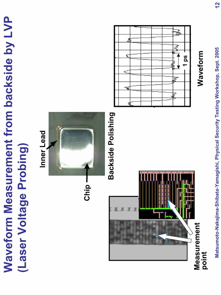
Wav
efor
m M
easu
rem
ent f
rom
bac
ksid
e by
LVP
(L
aser
Vol
tage
Pro
bing
)
Mea
sure
men
tpo
int
Bac
ksid
e Po
lishi
ng
Chi
p
Inne
r Lea
d
1 ps
Wav
efor
m

Mat
sum
oto-
Nak
ajim
a-Sh
ibat
a-Ya
mag
ishi
, Phy
sica
l Sec
urity
Tes
ting
Wor
ksho
p, S
ept.
2005
13
Det
ectio
n of
Pho
ton
Emis
sion
by
TRE
(Tim
e R
esol
ved
Emis
sion
)
VO
UT
VIN
VDD nM
OSF
ET
pMO
SFET
Emis
sion
Emis
sion
VIN
VOU
T
Tim
e (a
.u.)
IntensitynM
OSF
ETpM
OSF
ETPhoton
from
from
CM
OS
Inve
rter

Mat
sum
oto-
Nak
ajim
a-Sh
ibat
a-Ya
mag
ishi
, Phy
sica
l Sec
urity
Tes
ting
Wor
ksho
p, S
ept.
2005
14
Wav
efor
m M
easu
rem
ent b
y EO
-Sam
plin
gLa
ser
Elec
tric
Fiel
dEO C
ryst
alPa
d
Mirr
or
1µm
Wid
e ba
nd w
idth:~
60 G
Hz
EOC
ryst
alPola
rizat
ion
Cha
nge
Lase
r
Inte
nsity
Cha
nge
Pola
rizer
(Poc
kels
effe
ct)
~
Tim
e
Voltage
1 ns
60 mV

Mat
sum
oto-
Nak
ajim
a-Sh
ibat
a-Ya
mag
ishi
, Phy
sica
l Sec
urity
Tes
ting
Wor
ksho
p, S
ept.
2005
15
I-V C
hara
cter
istic
s M
easu
rem
ent b
y N
ano-
prob
er
Prob
e 2
Prob
e 1
Prob
e 3
Prob
e 4
5μm
Subs
trat
eG
ate
Dra
inSo
urce
Phot
ogra
ph o
f pro
bes
cont
actin
g to
via
plu
gsM
easu
red
I-V c
hara
cter
istic
s(A
: nor
mal
, B: f
ail)

Mat
sum
oto-
Nak
ajim
a-Sh
ibat
a-Ya
mag
ishi
, Phy
sica
l Sec
urity
Tes
ting
Wor
ksho
p, S
ept.
2005
16
Tam
perin
g Te
chni
ques
and
Rel
ated
Equ
ipm
ent
Dat
a re
adin
g fr
om R
OM
and
fla
sh m
emor
ies
FIB
, EB
T,LV
P,TR
E, E
OS
FIB
, OB
IC, S
EM
Cat
egor
ies
of a
ttack
Atta
ck T
echn
ique
s
Phys
ical
Str
uctu
re A
naly
sis
Chi
p re
mov
al fr
om IC
car
dsM
echa
nica
l sam
ple
trea
tmen
t
Cro
ss-s
ectio
nal a
naly
sis
Mem
ory
cell
stru
ctur
e an
alys
is
Circ
uit d
iagr
am a
naly
sis
Inte
rcon
nect
ion
laye
r lap
ping
w
ith s
tep
by s
tep
man
ner
Obs
erva
tion
of la
yout
pat
tern
sA
naly
sis
of c
ircui
t dia
gram
sfr
om la
yout
pat
tern
s
Ope
ratio
nal a
naly
sis
Pack
agin
g of
a re
mov
ed c
hip
Circ
uit r
erou
ting
base
d on
op
erat
iona
l circ
uit a
naly
sis
Sam
ple
prep
arat
ion
Ana
lysi
s of
chi
p ar
chite
ctur
e
Chi
p ar
chite
ctur
e an
alys
is
Equi
pmen
tH
ot p
late
,
FIB
, SEM
,
Cle
an b
ench
Lapp
ing
mac
hine
Mic
rosc
ope
(Eng
inee
rs)
Wire
bon
der,
Nan
o-pr
ober
Wav
efor
m m
easu
rem
ent
Mic
rosc
ope,
Cle
an b
ench
NC
-Grin
der,
Mat
sum
oto-
Nak
ajim
a-Sh
ibat
a-Ya
mag
ishi
, Phy
sica
l Sec
urity
Tes
ting
Wor
ksho
p, S
ept.
2005
17
4. A
Cas
e St
udy
of T
ampe
ring
Sens
or C
ircui
ts
–To
des
crib
e ho
w fa
ilure
ana
lysi
s te
chni
ques
can
be
used
for t
ampe
ring
IC c
ard
chip
s, w
e gi
ve s
ome
resu
lts
of a
n ex
perim
enta
l phy
sica
l atta
ck.
–In
gen
eral
, phy
sica
l atta
cks
may
hav
e tw
o ob
ject
ives
:
1.To
read
out
sec
ret d
ata
such
as
Crit
ical
Se
curit
y Pa
ram
eter
s fr
om th
e ch
ip.
2.To
alte
r the
func
tion
or d
ata
for s
ecur
ity
mec
hani
sms
impl
emen
ted
in th
e ch
ip.

Mat
sum
oto-
Nak
ajim
a-Sh
ibat
a-Ya
mag
ishi
, Phy
sica
l Sec
urity
Tes
ting
Wor
ksho
p, S
ept.
2005
18
Typi
cal F
unct
iona
l Blo
ck D
iagr
am o
f IC
Car
d C
hip
I/O CLK
RST VD
DG
ND
CPU
RO
M
Non
vola
tile
Mem
ory
RA
MSe
nsor
Cry
ptog
raph
icC
ircui
ts
Pow
er C
ontr
ol C
ircui
ts
I/OC
ircui
ts
Circ
uits
Stor
age
of G
loba
l
Stor
age
of A
ttack
Cry
ptog
raph
icD
ata
Proc
essi
ng
Mas
ter K
ey
His
tory
Prev
entio
n of
Ope
ratio
nU
nder
Irre
gula
r Con
ditio
n
: gen
eral
targ
et b
lock
s fo
r phy
sica
l atta
cks

Mat
sum
oto-
Nak
ajim
a-Sh
ibat
a-Ya
mag
ishi
, Phy
sica
l Sec
urity
Tes
ting
Wor
ksho
p, S
ept.
2005
19
An
Obs
erva
tion
on a
Tar
get C
hip
The
Shm
oo-P
lot
1.Th
e op
erat
iona
l ran
ge o
f su
pply
vol
tage
and
clo
ck
freq
uenc
yof
a ta
rget
IC c
ard
chip
was
mea
sure
d.
It is
som
ewha
t nar
row
erth
an
thos
e fo
r con
vent
iona
l LSI
ch
ips
fabr
icat
ed w
ith th
e sa
me
patte
rn ru
le.
Pass
Reg
ion
Fail
Reg
ion
Supp
ly V
olta
ge
Clock Frequency2.
Thi
s fa
ct s
tron
gly
sugg
ests
that
the
chip
is e
quip
ped
with
som
e se
nsin
g ci
rcui
try
for s
uppl
y vo
ltage
and
cl
ock
freq
uenc
yas
suc
h a
chip
ofte
n is
.

Mat
sum
oto-
Nak
ajim
a-Sh
ibat
a-Ya
mag
ishi
, Phy
sica
l Sec
urity
Tes
ting
Wor
ksho
p, S
ept.
2005
20
The
Ass
umpt
ion
–Th
e ta
rget
IC c
ard
chip
con
tain
s a
user
’s
pass
wor
d.
–A
n at
tack
er tr
ies
to fi
nd it
, by
exha
ustiv
e se
arch
, na
mel
y by
inpu
tting
eve
ry c
andi
date
pas
swor
d.
–H
owev
er, t
he h
isto
ry o
f bei
ng in
put w
rong
pa
ssw
ord
is re
cord
ed in
EEP
RO
M s
o th
at
the
IC c
ard
chip
may
be
forc
ed to
be
inac
tive
if th
e nu
mbe
r of a
ttack
tria
ls re
cord
ed in
EEP
RO
M
exce
eds
the
initi
ally
def
ined
thre
shol
d va
lue.

Mat
sum
oto-
Nak
ajim
a-Sh
ibat
a-Ya
mag
ishi
, Phy
sica
l Sec
urity
Tes
ting
Wor
ksho
p, S
ept.
2005
21
The
Atta
ck S
cena
rio
–Th
us a
pro
mis
ing
chal
leng
e of
the
atta
cker
may
be
dest
royi
ng th
e m
echa
nism
of w
ritin
g da
ta in
to
EEPR
OM
.
–If
the
supp
ly v
olta
ge m
ay b
e re
duce
d to
low
eno
ugh,
w
ritin
g da
ta in
to E
EPR
OM
may
no
long
er w
ork
and
the
atta
cks,
suc
h as
pas
swor
d ex
haus
tion,
cr
ypta
naly
sis,
or s
oftw
are
atta
cks,
can
be
done
re
peat
edly
.
–A
ttack
er tr
ies
to m
ake
the
supp
ly v
olta
ge s
enso
r ci
rcui
t ina
ctiv
e.

Mat
sum
oto-
Nak
ajim
a-Sh
ibat
a-Ya
mag
ishi
, Phy
sica
l Sec
urity
Tes
ting
Wor
ksho
p, S
ept.
2005
22
The
Flow
of E
xper
imen
tal P
hysi
cal A
ttack
Iden
tific
atio
n of
Tar
get S
enso
r Circ
uit P
ositi
ons
Targ
et S
enso
r Circ
uit D
iagr
am A
naly
sis
Inac
tivat
ion
of T
arge
t Sen
sor C
ircui
t by
Rer
outin
g
Ope
ratio
nal C
hara
cter
izat
ion
of IC
Car
d C
hip
Rea
d Se
cret
Dat
a
Rem
oval
and
Pac
kagi
ng o
f IC
Car
d C
hip

Mat
sum
oto-
Nak
ajim
a-Sh
ibat
a-Ya
mag
ishi
, Phy
sica
l Sec
urity
Tes
ting
Wor
ksho
p, S
ept.
2005
23
Rem
oval
and
Pac
kagi
ng o
f IC
Car
d C
hip
Chi
p

Mat
sum
oto-
Nak
ajim
a-Sh
ibat
a-Ya
mag
ishi
, Phy
sica
l Sec
urity
Tes
ting
Wor
ksho
p, S
ept.
2005
24
Iden
tific
atio
n of
Tar
get S
enso
r Circ
uit P
ositi
ons
Nor
mal
ope
ratio
n co
nditi
onEm
issi
on s
ites
incr
ease
due
tofa
ilure
. Em
issi
on M
icro
scop
y is
use
ful t
o id
entif
y se
nsor
circ
uits
.
(To
keep
the
secu
rity
of th
e re
al ta
rget
chi
p, th
e ab
ove
and
next
illus
trat
ive
pict
ures
are
the
resu
lts o
btai
ned
by e
xper
imen
ts o
n ot
her c
hips
.)

Mat
sum
oto-
Nak
ajim
a-Sh
ibat
a-Ya
mag
ishi
, Phy
sica
l Sec
urity
Tes
ting
Wor
ksho
p, S
ept.
2005
25
Targ
et S
enso
r Circ
uit D
iagr
am A
naly
sis
ML2
ML1
Gat
e la
yer
Out
put
Obs
erva
tion
Con
stru
ctio
nof
circ
uit
diag
ram

Mat
sum
oto-
Nak
ajim
a-Sh
ibat
a-Ya
mag
ishi
, Phy
sica
l Sec
urity
Tes
ting
Wor
ksho
p, S
ept.
2005
26
Rer
outin
g to
Mak
e Se
nsor
Circ
uit I
nact
ive
Out
put l
ine
Cut
poi
nt
Out
put l
ine
was
cut
and
con
nect
ed to
Vss
line
.
New
ly fo
rmed
line
by F
IBC
ut p
oint
New
ly fo
rmed
Line
by
FIB

Mat
sum
oto-
Nak
ajim
a-Sh
ibat
a-Ya
mag
ishi
, Phy
sica
l Sec
urity
Tes
ting
Wor
ksho
p, S
ept.
2005
27
Shm
oo-P
loto
f IC
Car
d C
hip
Bef
ore
and
Afte
rA
ltera
tion
of S
enso
r Circ
uits
for
Low
Sup
ply
Volta
ge a
nd L
ow C
lock
Fre
quen
cy
Pass
Reg
ion
Fail
Reg
ion
Supp
ly V
olta
ge
Clock Frequency
(Initi
al)
Afte
r alte
ratio
n

Mat
sum
oto-
Nak
ajim
a-Sh
ibat
a-Ya
mag
ishi
, Phy
sica
l Sec
urity
Tes
ting
Wor
ksho
p, S
ept.
2005
28
Supe
riorit
y th
e Li
ght E
mis
sion
Imag
e (L
EI) o
ver
the
Volta
ge C
ontr
ast I
mag
e (V
CI)
of E
B T
estin
g
Con
tras
t im
age
diffe
renc
ebe
twee
n op
erat
ing
cond
ition
of A
and
B.
(IFA
: Im
age
Faul
t Ana
lysi
s)
Emis
sion
imag
e di
ffere
nce
betw
een
oper
atin
g co
nditi
onof
A a
nd B
.

Mat
sum
oto-
Nak
ajim
a-Sh
ibat
a-Ya
mag
ishi
, Phy
sica
l Sec
urity
Tes
ting
Wor
ksho
p, S
ept.
2005
29
Ana
lyze
d C
ircui
ts A
rea
is L
ess
Than
2%
of
the
Are
a of
the
Chi
p Ex
clud
ing
the
Mem
ory
Ana
log
and
Dig
ital C
ircui
t Are
a
Ana
lyze
d Se
nsor
Circ
uit A
rea
Mem
ory
Are
a

Mat
sum
oto-
Nak
ajim
a-Sh
ibat
a-Ya
mag
ishi
, Phy
sica
l Sec
urity
Tes
ting
Wor
ksho
p, S
ept.
2005
30
5. A
Ten
tativ
e C
lass
ifica
tion
of S
ecur
ity L
evel
s
–Ba
sed
on o
ur e
xper
ienc
e in
failu
re a
naly
sis,
we
sugg
est
a te
ntat
ive
way
of c
lass
ifyin
g se
curit
y le
vels
of L
SI c
hips
.
–Th
e se
curit
y le
vels
may
be
clas
sifie
d by
usi
ng
(1)t
he re
quire
d sk
ill ra
nk o
f the
atta
cker
s or
an
alys
ts,
and
(2)t
he n
eces
sary
failu
re a
naly
sis
equi
pmen
t an
d its
cos
t to
atta
ck th
e ch
ips.
–O
ur a
ttem
pt o
f suc
h a
clas
sific
atio
n is
not
yet
mat
ured
an
d sh
ould
be
impr
oved
bas
ed o
n m
uch
disc
ussi
on.

Mat
sum
oto-
Nak
ajim
a-Sh
ibat
a-Ya
mag
ishi
, Phy
sica
l Sec
urity
Tes
ting
Wor
ksho
p, S
ept.
2005
31
Def
initi
on o
f Ski
ll R
anks
LSI a
rchi
tect
ure
Logi
c an
d an
alog
circ
uit
oper
atio
n
Mem
ory
circ
uit o
pera
tion
Mem
ory
cell
stru
ctur
e
Proc
ess
tech
nolo
gy
Mea
sure
men
t tec
hnol
ogy
Expe
rienc
e (m
inim
um y
ears
)
Skill
Ran
kSk
ill c
ompo
nent
Failu
re a
naly
sis
tech
nolo
gy
Expe
rtcl
ass
clas
scl
ass
clas
scl
ass
1st
2nd
3rd
4th
5th 3
58
10
13
15
clas
s
α: e
xper
t, β
: pro
ficie
nt, γ
: suf
ficie
nt
α α α α α α
α
α
α ααα α
α α α α
ββ β β
β β β ββ
β β β
γ
γγ
γ
γ γ γ γ
α> β
> γ

Mat
sum
oto-
Nak
ajim
a-Sh
ibat
a-Ya
mag
ishi
, Phy
sica
l Sec
urity
Tes
ting
Wor
ksho
p, S
ept.
2005
32
Tent
ativ
e C
andi
date
of F
ive
Secu
rity
Leve
ls o
f LSI
Chi
ps
Bas
ed o
n Fa
ilure
Ana
lysi
s Eq
uipm
ent a
nd S
kills
of A
naly
st
“Bey
ond”
mea
ns th
e le
vel n
on-a
ttack
able
by
toda
y’s
FA
tech
nolo
gies
.
Skill
rank
Nec
essa
ry F
A e
quip
men
tSe
curit
yle
vel
tota
l cos
t[M
$]
A (
+2)
C (
0 )
D (
-1)
E (-
2)
B (
+1)
Expe
rt
1st
2nd
3rd
4th,
5th
6.5+
3.5
10+6
2.5+
4
Nan
o-pr
ober
LVP
TRE
Cle
an b
ench
EOS
LEM
/CC
D
LEM
/MC
T
EBT
SEM
OB
IC
Hot
-pla
te
Wire
-bon
derFI
BLa
ppin
g M
achi
ne
Elec
tric
al m
easu
rem
ent
syst
em
Rev
erse
eng
inee
ring
softw
are
0.5+
2
0.5
Equi
pmen
t
Bey
ond
Unk
now
n (to
day)
??
Cur
rent
ave
rage
failu
re
anal
ysis
cap
abili
ty m
ay
corr
espo
nd to
“le
vel C
”.
Mat
sum
oto-
Nak
ajim
a-Sh
ibat
a-Ya
mag
ishi
, Phy
sica
l Sec
urity
Tes
ting
Wor
ksho
p, S
ept.
2005
33
6. S
umm
ary
–W
e ha
ve d
escr
ibed
rela
tions
hips
bet
wee
n LS
I tam
per
resi
stan
ce a
nd F
A te
chni
ques
.
–Ta
mpe
r res
ista
nce
of L
SI c
hips
aga
inst
phy
sica
lat
tack
s sh
ould
be
eval
uate
d or
test
ed o
n th
e ba
sis
of
late
st te
chno
logi
es.
–To
faci
litat
e an
und
erst
andi
ng o
f the
leve
l of t
oday
’s
failu
re a
naly
sis
tech
niqu
es w
e ha
ve d
emon
stra
ted
an
inac
tivat
ion
of s
enso
r circ
uits
whe
re e
mis
sion
m
icro
scop
y pl
ays
an im
porta
nt ro
ll.
–Th
en w
e ha
ve g
iven
a te
ntat
ive
way
of c
lass
ifyin
g th
e se
curit
y le
vels
for L
SI c
hips
with
resp
ect t
o th
e re
quire
d eq
uipm
ent a
nd th
e re
quire
d sk
ills o
f atta
cker
s.

Mat
sum
oto-
Nak
ajim
a-Sh
ibat
a-Ya
mag
ishi
, Phy
sica
l Sec
urity
Tes
ting
Wor
ksho
p, S
ept.
2005
34
Ref
eren
ces
[1] S
. Nak
ajim
a an
d T.
Tak
eda,
"Fa
ilure
ana
lysi
s in
hal
fmic
ron
and
quar
term
icro
ner
as, "
Pr
ocee
ding
of t
he 6
th E
urop
ean
Sym
posi
um o
n R
elia
bilit
y of
Ele
ctro
n D
evic
es,
Failu
re P
hysi
cs a
nd A
naly
sis
(ESR
EF 9
5), p
p. 2
73-2
80, 1
995.
[2] S
. Nak
ajim
a, T
. Uek
i, Y.
Shio
noya
, K.M
afun
e, N
.Kuj
i, S.
Nak
amur
a, Y
.Kom
ine
and
T. T
aked
a, "
Cur
rent
sta
tus
of fa
ilure
ana
lysi
s fo
rULS
Is, "
Mic
roel
ectr
onic
s R
elia
bilit
y,Vo
l. 38
, pp.
136
9-13
77, 1
998.
[3] S
. Nak
ajim
a, S
. Nak
amur
a, K
.Kuj
i, T.
Uek
i, T.
Ajio
kaan
d T.
Sak
ai, "
Con
stru
ctio
n of
a
cost
-effe
ctiv
e fa
ilure
ana
lysi
s se
rvic
e ne
twor
k ---
Mic
roel
ectr
onic
failu
re
anal
ysis
ser
vice
in J
apan
," M
icro
elec
tron
ics
Rel
iabi
lity,
Vol
. 42,
pp.
511-
521,
200
2.
[4] Y
. Mits
ui, e
t al,
"Phy
sica
l and
che
mic
al a
naly
tical
inst
rum
ent f
or fa
ilure
ana
lyse
sin
G-B
it de
vice
s, "
Tech
nica
l Dig
est o
f Int
erna
tiona
l Ele
ctro
n D
evic
es M
eetin
g,
pp.3
29-3
32, 1
998.
[5] C
. Has
him
oto,
T. T
akiz
awa,
S. N
akaj
ima,
M. S
hina
gaw
a an
d T.
Nag
atsu
ma,
"O
bser
vatio
n of
the
inte
rnal
wav
efor
ms
in h
igh-
spee
d hi
gh-d
ensi
tyLS
Isus
ing
an E
OS
prob
er, "
Mic
roel
ectr
onic
s R
elia
bilit
y, V
ol. 4
1, p
p. 1
203-
1209
, 200
1.[6
] M. K
. Mc
Man
us, J
. A.K
ash,
S. E
. Ste
en, S
.Pol
onsk
y, J
. C. T
sang
, D. R
.Kne
bela
nd
W.H
uott,
"PIC
A: B
acks
ide
failu
re a
naly
sis
of C
MO
S ci
rcui
ts u
sing
Pic
osec
ond
Imag
ing
Circ
uit A
naly
sis,
" M
icro
elec
tron
ics
Rel
iabi
lity,
Vol
. 40,
pp.
135
3-13
58, 2
000.
[7
] A.T
osi,
F.St
ella
ri, F
.Zap
paan
d S.
Cov
a, "
Bac
ksid
e Fl
ip-C
hip
test
ing
by m
eans
of
high
-ban
dwid
th lu
min
esce
nce
dete
ctio
n,"
Mic
roel
ectr
onic
s R
elia
bilit
y,Vo
l. 43
, pp
. 166
9-16
74, 2
003.