s. k. sharma khuram ali editors solar cells
TRANSCRIPT

S. K. SharmaKhuram Ali Editors
Solar CellsFrom Materials to Device Technology

Solar Cells

S. K. Sharma • Khuram AliEditors
Solar CellsFrom Materials to Device Technology
123

EditorsS. K. SharmaDepartment of Physics, Faculty of Scienceand TechnologyThe University of the West IndiesSt. Augustine, Trinidad and Tobago
Khuram AliDepartment of PhysicsUniversity of Agriculture FaisalabadFaisalabad, Pakistan
ISBN 978-3-030-36353-6 ISBN 978-3-030-36354-3 (eBook)https://doi.org/10.1007/978-3-030-36354-3
© Springer Nature Switzerland AG 2020This work is subject to copyright. All rights are reserved by the Publisher, whether the whole or partof the material is concerned, specifically the rights of translation, reprinting, reuse of illustrations,recitation, broadcasting, reproduction on microfilms or in any other physical way, and transmissionor information storage and retrieval, electronic adaptation, computer software, or by similar or dissimilarmethodology now known or hereafter developed.The use of general descriptive names, registered names, trademarks, service marks, etc. in thispublication does not imply, even in the absence of a specific statement, that such names are exempt fromthe relevant protective laws and regulations and therefore free for general use.The publisher, the authors and the editors are safe to assume that the advice and information in thisbook are believed to be true and accurate at the date of publication. Neither the publisher nor theauthors or the editors give a warranty, expressed or implied, with respect to the material containedherein or for any errors or omissions that may have been made. The publisher remains neutral with regardto jurisdictional claims in published maps and institutional affiliations.
This Springer imprint is published by the registered company Springer Nature Switzerland AGThe registered company address is: Gewerbestrasse 11, 6330 Cham, Switzerland

Preface I
Solar cell is designed to convert sunlight into electrical power using photovoltaicproperties. The advantage of a solar cell resides in a nearly permanent, uninter-rupted power source at a minimal operating cost. Moreover, it has the ability toconvert sunlight directly into electricity instead of some intermediate form ofenergy. A higher power to weight ratio is another advantage the solar cells have ascompared to other power sources such as batteries. On the other hand, the lowpower to unit area of sunlight ratio (which necessitates using large area arrays), therelatively low efficiency, and the degradation that takes place in hostile high-energyradiation environments are some of their main disadvantages. The role played bysolar cells in a wide range of resource investigation, meteorological, broadcast,communications, scientific, and space development research cannot be denied. Itcan be rightly commented that without the development of solar cells, we would nothave the sophisticated weather, communications, military, and scientific satellitecapabilities that we have today. Increased life, improved conversion efficiency, andreduced cost are the basic objectives for research and development of solar cellmaterials.
Thin-film technology has been significantly improved since the last few years.For sufficient absorption of the solar spectrum, it is required that the wafer thicknessshould be >700 µm. It is not desirable for commercial or large-scale production ofsolar cells because it is a large thickness for a Si wafer in terms of cost and effectivecollection of photo-generated carriers. This type of solar cell is generally made bydepositing one or more thin films, on a glass, plastic, or metal substrates. Initially,wafers of up to 200 µm thickness were used to fabricate silicon-based thin-filmsolar cells. This technique allows thin-film cells to be flexible and lower in weight.However, it is also mandatory to have a general understanding of the problems thatappear when the thickness of a silicon wafer is decreased. Incorporating quantumdots is an updated approach to harness solar cells. Efficiency of thin-film-basedsolar cells has been remarkably increased with the addition of quantum dots. Theyhave properties of band gap tunability, which makes them suitable for multijunctionsolar cells. Quantum dots have energy levels that are tunable by altering their size.These tunable energy levels, in turn, determine the band gap. Quantum dots in
v

semiconductors are nowadays a subject of great importance primarily due to theirelectronic structures and tunable optoelectronic characteristics. In addition, bandgaps for single-junction solar cells using lead sulfide (PbS) colloidal quantum dots(CQD) can be fabricated which can operate on far infrared frequencies. Suchconfiguration is difficult to achieve with conventional solar cells. Currently,quantum dot-based nanostructures have been primarily restricted to lasers, sensors,and LEDs, etc. However, the blue shift in the band gap energy and thesize-dependent increase in oscillator strength are the characteristics that can be usedfor promoting better photovoltaic devices as compared to traditional photovoltaics.Solar cells with multiple stacked p–n junctions are made with multiple layeredsemiconducting materials from III–V compound semiconductors. These types ofIII–V cells have the highest conversion efficiency under concentrated sunlight.Since their evolution, the multijunctions solar cells have achieved great attention inthe photovoltaic industry due to broad choice of materials with direct band gaps andhigh absorption coefficients. However, manufacturing price and process complex-ities are also involved with the high efficiencies gained in III–V multijunction solarcells.
Recently, organic–inorganic hybrid solar cells have gained a rapid improvementin their performance. Their overall power conversion efficiency (PCE) has exceeded20% because of high charge carrier mobility, efficient light harvesting, and longcarrier lifetime. A perovskite absorption layer is sandwiched between a hole contactlayer and an electron contact layer in a typical planar heterojunction perovskitesolar cell. Irrespective of the compatibility of low-temperature sputtered NiOx filmswith flexible devices, their low PCE (below 10%) makes them unappealing to theresearch community. Therefore, for flexible perovskite solar cells, it is very pur-poseful to explore low-temperature processed NiOx films with effective holeextraction capabilities. It is observed that on an ITO glass substrate, asolution-derived NiOx hole contact layer-based inverted planar heterojunctionperovskite solar cell can gain a PCE of as high as 16.47%. Before this technology isfully accepted in the market, many hurdles need to be overcome. At this time,organic photovoltaics (OPVs) are applicable only in limited markets that requirelightweight, flexibility, stability, and variable angle performance. The continuousdevelopment of OPV with the improvement in their light harvesting ability and themanagement of active layer materials will occasion widely applicable technologiesfor electrical generation.
St. Augustine, Trinidad and Tobago S. K. SharmaFaisalabad, Pakistan Khuram Ali
vi Preface I

Preface II
Reducing the cost and increasing the conversion efficiency are the crucial tasks inorder to make solar cell energy competitive. Though important progress has beenmade in recent years, a complete auxiliary of traditional energy sources by solarcells still requires improvement in device performance.
This book is devoted to the rapidly developing class of solar cell materials anddesigned to provide much needed information on the fundamental scientific prin-ciples of these materials, together with how these are employed in photovoltaicapplications.
Moreover, a special emphasize has been given for their space applications bythorough study of radiation-tolerant solar cells. This book will present compre-hensive research outlining progress on the synthesis, fabrication, and application ofsolar cell materials from fundamental to device technology.
St. Augustine, Trinidad and Tobago S. K. Sharma
vii

Contents
Synthesis and Processing of Nanomaterials . . . . . . . . . . . . . . . . . . . . . . 1Muhammad Yasin Naz, Shazia Shukrullah, Abdul Ghaffar, Khuram Aliand S. K. Sharma
Perspective of Nanomaterials in the Performance of Solar Cells . . . . . . 25Hafiz Muhammad Asif Javed, Wenxiu Que, Muhammad Raza Ahmad,Khuram Ali, M. Irfan Ahmad, Anam ul Haq and S. K. Sharma
Materials for Solar Cell Applications: An Overview of TiO2, ZnO,Upconverting Organic and Polymer-Based Solar Cells . . . . . . . . . . . . . . 55Navadeep Shrivastava, Helliomar Barbosa, Khuram Ali and S. K. Sharma
Recent Advances in Solar Cells . . . . . . . . . . . . . . . . . . . . . . . . . . . . . . . 79Marcio A. P. Almeida
Photovoltaic Materials Design by Computational Studies:Metal Sulfides . . . . . . . . . . . . . . . . . . . . . . . . . . . . . . . . . . . . . . . . . . . . . 123Edan Bainglass, Sajib K. Barman and Muhammad N. Huda
Photovoltaic-Based Nanomaterials: Synthesis and Characterization . . . . 139Kanwal Akhtar, Naveed Akhtar Shad, M. Munir Sajid, Yasir Javed,Muhammad Asif, Khuram Ali, Hafeez Anwar, Yasir Jamiland S. K. Sharma
Carbon Nanotubes: Synthesis and Application in Solar Cells . . . . . . . . 159Shazia Shukrullah, Muhammad Yasin Naz, Khuram Ali and S. K. Sharma
Basic Concepts, Engineering, and Advances in Dye-SensitizedSolar Cells . . . . . . . . . . . . . . . . . . . . . . . . . . . . . . . . . . . . . . . . . . . . . . . 185Mohan Chandra Mathpal, Promod Kumar, F. H. Aragón,Maria A. G. Soler and H. C. Swart
Quantum Dot Solar Cells . . . . . . . . . . . . . . . . . . . . . . . . . . . . . . . . . . . . 235Hafeez Anwar, Iram Arif, Uswa Javeed, Huma Mushtaq, Khuram Aliand S. K. Sharma
ix

Organometal Halide Perovskite-Based Materials and TheirApplications in Solar Cell Devices . . . . . . . . . . . . . . . . . . . . . . . . . . . . . 259Amna Bashir and Muhammad Sultan
Effect of Oxygen Vacancies in Electron Transport Layer forPerovskite Solar Cells . . . . . . . . . . . . . . . . . . . . . . . . . . . . . . . . . . . . . . . 283Mohamad Firdaus Mohamad Noh, Nurul Affiqah Arzaeeand Mohd Asri Mat Teridi
Solar Cells and Optoelectronic Devices in Space . . . . . . . . . . . . . . . . . . 307Khuram Ali, Syedda Shaher Bano, Hasan M. Khan and S. K. Sharma
Multi-junction (III–V) Solar Cells: From Basics to AdvancedMaterials Choices . . . . . . . . . . . . . . . . . . . . . . . . . . . . . . . . . . . . . . . . . . 325Khuram Ali, Afifa Khalid, Muhammad Raza Ahmad, Hasan M. Khan,Irshad Ali and S. K. Sharma
x Contents
Synthesis and Processingof Nanomaterials
Muhammad Yasin Naz, Shazia Shukrullah, Abdul Ghaffar, Khuram Aliand S. K. Sharma
Abstract Nanomaterials have emerged as a distinct class ofmodernmaterials. Thesematerials are of significant importance due to their unique optical, electrical, thermal,and magnetic properties. Due to their tunable physical and chemical characteristics,including melting point, electrical conductivity, wettability, heat conductivity, lightabsorption, catalytic activity, and scattering, these materials have also gained recog-nition in high-tech engineering applications. These characteristics reflect better per-formance and working efficiency of nanomaterials relative to their bulk counterparts.Although there are many naturally occurring nanomaterials, most nanomaterials areengineered in laboratories. Such materials are purposefully synthesized in accor-dance with the industrial requirements. This chapter deals with the fundamentals ofnanomaterials, their history, properties, and industrial applications. Different meth-ods of synthesis of nanomaterials, their merits, demerits, and scale-up potential arealso discussed in this chapter.
Keywords Nanomaterials · Properties of nanomaterials · Synthesis routes ·Chemical vapor deposition
1 Fundamentals of Nanomaterials
1.1 Introduction to Nanomaterials
Nanomaterials are representing a major area of science and technology with fullgrowth in numerous application domains. These materials have gained fame in high-tech advancements due to their tunable physical and chemical traits, including melt-ing point, electrical conductivity, wettability, thermal conductivity, light absorption,
M. Y. Naz (B) · S. Shukrullah · A. Ghaffar · K. AliDepartment of Physics, University of Agriculture, Faisalabad 38040, Pakistane-mail: [email protected]
S. K. SharmaDepartment of Physics, Faculty of Science and Technology, The University of the West Indies,St. Augustine, Trinidad and Tobago
© Springer Nature Switzerland AG 2020S. K. Sharma and K. Ali (eds.), Solar Cells,https://doi.org/10.1007/978-3-030-36354-3_1
1

2 M. Y. Naz et al.
catalytic activity, and scattering. These traits reflect the improved performance ofnanomaterials as compared to their bulk counterparts. The International Organiza-tion for Standardization defines the nanomaterial as a “material having external orinternal nanoscale dimensions or surface structure” [1, 2]. Presently, the followingscientific terms are being used for the materials with nanoscale dimensions [1–3].
• Nanoscale: Roughly, the sizes in the range of 1–100 nm.• Nanoscience: The study of materials at nanoscale to understand their size andstructural properties, to compare the advent of individual atoms and molecules,and to understand the bulk material related differences.
• Nanotechnology: Practical use of the scientific knowledge to manipulate andcontrol thematter on the nanoscale dimensions for different industrial applications.
• Nanomaterial: A material with external or internal dimensions on the nanoscale.• Nano-object: A material possessing one or more peripheral dimensions atnanoscale.
• Nanoparticle: An object with all three external dimensions grown at nanoscaleis called nanoparticles. If the shortest and longest axes lengths of the object aredifferent, then it is referred to as a nanorod or nanoplate instead of nanoparticles.
• Nanofiber: A nanomaterial with two similar dimensions, extending at nanoscale,and a longer third dimension is called nanofiber.
• Nanocomposite: A multiphase material having at least one phase on nanoscale.• Nanostructure: Arrangement of interconnected constituent parts in the nanoscaleregion.
• Nanostructured material: A material with nanoscale structural dimensions.
Nanomaterials are the keystones of nanoscience and technology. Nanotechnologyis widely known as an interdisciplinary research area, which has been recognizedworldwide during the past few years. Nanotechnology has shown substantial com-mercial impact, which will grow exponentially in the coming years [4]. Figure 1depicts the evolution of science and technology of materials over time [1, 5, 6]. Thischapter is aimed at a review of the progress to date in the science and technologyof ultrafine particles, which form the building blocks of nanomaterials. An attemptis made to outline the progression of nanomaterials from fundamental research andcommercial standpoint.
1.2 History of Nanomaterials
The nanomaterials, driven from nanoparticles, have evolved as a distinct class ofmaterials [7]. These materials are of special interest due to their unique optical,electrical, thermal, magnetic, and other properties [4]. Materials with dimensions inmicrometers mostly reveal the physical characteristics same as the bulk materials.Contrarily, materials with dimensions in nanometers exhibit physical characteristicstotally different from the bulk. In this size range, the materials exhibit some amazingproperties since transitions from bulk form to atoms and/or molecules take place. For

Synthesis and Processing of Nanomaterials 3
Fig. 1 Evolution of science and technology over time
example, nanosized crystals may have very low melting points and the differencecan be up to 1000 °C. Also, lattice constant may decrease due to the appearanceof surface atoms or ions as a significant fraction of a total number of atoms orions. The surface energy, associated with these species, plays a substantial role inthermal stability of the material [5]. Very first scientific report on nanomaterials waspublished by Michael Faraday in 1857. He was the first who synthesized colloidalgold particles. Nanocatalysts have also remained under investigation for the last70 years. In early the 1940s, the nanoparticles of precipitated and fumed silica werebeing sold in Germany and America as rubber reinforcement. The silica was beingused as a substitute for ultrafine carbon black. The nanosized silica has found manyapplications in everyday consumer products, including nondairy coffee creamer,optical fibers, automobile tires, and catalyst supports.
During 1960–70, nanopowders of metals were developed for magnetic recordingtapes. Granqvist and Buhrman, 1976, reported the production of nanocrystals froman inert gas evaporation technique. In recent years, several structural and functionalmaterials have been developed through nanophase engineering for manipulation ofcatalytic, mechanical, electrical, magnetic, electronic, and optical functions. Thesematerials include both organic and inorganic structures [4, 8].
1.3 Nanomaterials Are All Around Us
Althoughmany nanomaterials exist naturally, majority of the nanomaterials are engi-neered. They are designed and synthesized according to the needs of commercial pro-cesses and products. Synthetic nanomaterials are being used in sunscreens, sportinggoods, cosmetics, stain-resistant tires, clothing, electronics, andmany other everyday

4 M. Y. Naz et al.
items. In medicine, these materials are being used for imaging, diagnosis, and drugdelivery. The unique properties of nanoscale are attributed to an increase in relativesurface area and appearance of new quantum effects. The high surface area to volumeratio of nanomaterials improves their mechanical strength and chemical reactivity.Also, the quantum effects at nanoscale become more significant in determining thecharacteristics of the materials [4].
Nanoparticles can be treated as a common type ofmaterials inmany different envi-ronments. These particles pass by almost undetected unless somebody is looking forthem. Nanoparticles are being produced through different physical and chemical pro-cesses. The volcanic ash, fine sand, dust, ocean spray, and even biological matter arethe natural sources of nanoparticles [9]. The synthetic or anthropogenic nanoparti-cles are classified into incidental nanoparticles and engineered nanoparticles. Thesize and shape of the incidental nanoparticles are poorly controlled. These arethe by-products of human activities and are made of a hodge-podge of the elements.The major sources of incidental nanoparticles are diesel engines, fire, and large-scalemining [9]. Figure 2 shows the common sources of incidental nanoparticles.
Engineered nanoparticles are specifically designed and synthesized through dif-ferent physical and chemical processes. It is possible to control their size, shape, andcompositions by deliberately choosing the synthesis technique. Although engineerednanoparticles are becoming more sophisticated over time, the simple nanoparticlesproduced through relatively easy chemical reactions [9]. The nanophase ceramics,nanostructured semiconductors, nanosized metallic powders, single nanosized mag-netic particles, nanostructured metal clusters, nanostructured metal-oxide thin films,and polymer-based composites are few examples of engineered nanomaterials.
Fig. 2 Few sources of incidental nanoparticles

Synthesis and Processing of Nanomaterials 5
2 Properties of Nanomaterials
The factors making the nanomaterials considerably different from their bulkcounterparts are:
I. Large surface area to volume ratio.II. Quantum confinement effect.
2.1 Surface Area of Nanomaterials
Nanomaterials possess the large surface area to volume ratio. The ratio of the atomsat the surface to those within the body changes dramatically on a successive divisionof a macroscopic object into smaller ones [5]. The constituent particles exhibit arelatively larger surface area to volume ratio when compared to same mass of thematerial in bulk form. Figure 3 shows a cube of 1 m3 volume 6 m2 surface area.If divided into eight smaller cubes, the surface area would increase to 12 m2. Thesurface area would increase further by cutting down the cube in a large number ofsmaller particles. In response, the surface atomswill increase bymaking thematerialschemically more reactive.
Fig. 3 Illustration of surface area to volume ratio

6 M. Y. Naz et al.
2.2 Quantum Confinement
The bulk materials are known for continuous electronic energy levels. Contrarily, thenanomaterials do not have continuous energy levels due to confinement of electronicwave function in one, two, or three physical dimensions. The quantum confinementof nanomaterials can be classified as:
I. 1-D confinement—thin film, quantum well.II. 2-D confinement—nanotubes, nanorod, and quantum wire.III. 3-D confinement—precipitates, colloids, and quantum dots.
2.3 Structural Properties of Nanomaterials
Themechanical properties of nanomaterials are of quite basic interest since it is prob-lematic to growmacroscopic objects of high density and grain size less than 100 nm.However, two materials have attracted the interest and achieved the industrial impor-tance. These materials are plastic-deformed metals and the polymers compositedwith nanotubes or nanoparticles. However, earlier is not accepted as a nanomaterialdue to its larger grain size. The experimental investigations on structural traits of bulknanomaterials are impaired by the main experimental problems in synthesizing thespecimens of fairly defined porosities and grain sizes. Therefore, molecular dynam-ics and model calculations are of key importance for understanding the structuralproperties of such materials [10].
The addition of nanoparticles, nanorods, or nanotubes into polymers significantlyimproves their structural properties. Possible changes in structural properties dependon the filler type and the method of conducting filling. The filling method is of greatimportance because the anticipated advantages filling may lose if the filler particlesaggregate into larger particles. The polymers filled with nanofillers exhibit a widerange of failure strengths and strains, depending on the shape and particle size ofthe filler and the degree of agglomeration. The polymers reinforced with silicateplatelets have shown the best structural properties of economic relevance. Althoughnanofibers or nanotubes added polymers are the best composites, sometimes thesecomposites exhibit the least ductility. On the other hand, the composites filled withcarbon nanotubes may exhibit high mechanical strength and strain at rupture [4, 11].
2.4 Chemical Properties of Nanomaterials
The small atomic clusters exhibit high ionization energy as compared to the corre-sponding bulk material. Owing to different crystallographic structures and high sur-face area to volume ratio, the nanomaterials exhibit high radical alteration in chemical

Synthesis and Processing of Nanomaterials 7
reactivity. The catalysis, utilizing nanoscale systems, can significantly increase theselectivity, rate, and efficiency of a chemical reaction. Porosity and surface areaof nanomaterials are important physical properties influencing the utility, quality,and handling of the nanomaterials. Therefore, these materials should carefully beengineered to carry out specific functions. For example, surface chemistry of car-bon nanotubes is driven by the surface defects and basal and edge carbon atoms.The structural defects of graphene layer or nanotubes act as active sites because ofincreased density of unpaired electrons. These active sites determine the rate andefficiency of the reactions [12, 13].
2.5 Magnetic Properties of Nanomaterials
Magnetite nanoparticles are found in animal cells, which help them in cruising. Themost fascinating characteristic of magnetic nanoparticles is the lessening of multi-domains into a single domain with a reduction of particle size to some limit [14].These materials have multifunction applications, such as color imaging, ferrofluids,bioprocessing, magnetic storage devices, and refrigeration. A high proportion ofsurface atoms in magnetic nanomaterials develops different magnetic coupling withneighboring atoms and consequently different magnetic properties than the bulkcounterpart. As shown in Fig. 4, the bulk ferromagnetic materials have multiplemagnetic domains. In contrast, magnetic nanoparticles often have a single magneticdomain exhibiting the superparamagnetism phenomenon [4, 15].
The gold and platinum are non-magnetic in bulk form and magnetic at nanoscale.In such materials, the surface atoms not only differ from bulk atoms but also exhibitdifferent properties due to interaction with other species. The interaction of nanopar-ticles with other chemical species modifies their physical characteristics by cappingthem with molecules.
Fig. 4 Illustration ofsuperparamagnetism innanomaterials

8 M. Y. Naz et al.
The large spin–orbit coupling of these noble metals can yield to a large anisotropyand therefore exhibit high ordering temperatures.More surprisingly, permanentmag-netism was observed up to room temperature for thiol-capped Au nanoparticles. Fornanoparticles with sizes below 2 nm, the localized carriers are in the 5d band. BulkAu has an extremely low density of states and becomes diamagnetic, as is also thecase for bare Au nanoparticles. This observation suggested that modification of thed band structure by chemical bonding can induce ferromagnetic like character inmetallic clusters [4].
2.6 Optical Properties of Nanomaterials
The optical aspect of nanomaterials is also fascinating for many communicationapplications. Themost important applications utilizing the optical properties of nano-materials are the optical detectors, sensors, lasers, imaging devices, optical displays,phosphor, solar cell, photocatalysis, biomedicine, and photo-electrochemistry [4].The optical absorption and emission in bulk materials depend on transitions betweenvalence bands and conduction bands. The low dimensional metals and semiconduc-tors exhibit large changes in their optical properties, such as color. For example, thecolloidal solution of gold nanoparticles has typical deep red color when particle sizeis very small. However, the color of solution changes to yellow with an increase inparticle size. This change in color with size is attributed to the resonance of surfaceplasmons, which normally occurs in low dimensional materials.
The frequency and intensity of light, emitted from the nanoparticles, also dependon the size of the particle. The size of the nanoparticles of semiconductors in theform of quantum dots effects their nonlinear optical properties and gain for cer-tain emission wavelengths. Other characteristics influenced by the small dimensionsinclude photocatalysis, photoemission, photoconductivity, and electroluminescence.The spacing between energy levels increases with a decrease in particle size, whichhelps confining the system and enhancing the surface plasmon resonance. The reso-nance of surface plasmons is related to the coherent excitation of free electrons in theconduction bands, which results in in-phase oscillations. The free electrons polarizerelative to cationic lattice due to electric field of incoming light. A net charge differ-ence appears at the boundaries of nanoparticle, which acts as a restoring force. Thisforce sets the electrons into dipolar oscillation at a certain frequency. The energy ofsurface plasmon resonance is governed by the dielectric medium around the nanopar-ticles and free electrons’ density. The resonance sharpens with increase of particlesize. The larger particles enhance the scattering length. The resonance frequency ofall the noble metals falls in the visible region of the light spectrum [5, 11].

Synthesis and Processing of Nanomaterials 9
2.7 Electronic Properties of Nanomaterials
How the particle size influences the electrical conductivity of nanomaterials is a com-plex phenomenon?The electrical conductivity is based on distinctmechanismswhichare classified into grain boundary scattering, surface scattering, quantized conduc-tion, ballistic conduction, widening and reduction of band gap, Coulomb chargingand tunneling and a change in microstructures. An increased perfection, reducedimpurity, minimum dislocation, and low structural defects also influence the elec-trical conductivity nanomaterials [5]. Only one electron wave mode is observed inelectrically conducting carbon nanotubes. This mode transports the electrical cur-rent through the nanotubes. Since orientation and length of carbon nanotubes vary,these tubes would touch the mercury surface at different times by providing a set ofinformation. This information is about the resistance of different nanotubes and theeffect of tube length on resistance [4].
Changes in electronic properties of low dimensional materials are related to thewave-like properties of the electrons and scarcity of the scattering centers. Whenthe system size is comparable to the de Broglie wavelength of electrons, the energystates exhibit a more pronounced discrete nature. In some cases, the conductorschange to insulators when the size is well below the critical length scale. Conductionin extremely enclosed structures such as quantum dot is very susceptible to thepresence of other charge carriers, and hence, the dot charge state is known as theCoulomb blockade effect. This results in single electrons conduction procedures thatin turn require a minimum quantity of energy to run the switch, memory elements,or transistor [15].
3 Common Synthesis Techniques
Nanomaterial synthesis techniques are split into two primary groups, namely top-down approaches and bottom-up approaches. Thesemethods are used for assemblingatoms together or disassembling or dissociating bulk materials into finer parts madeup of very few atoms. The top-down approach begins with larger objects as shownin Fig. 5, which are reduced to lower sizes to achieve fine features and nanoscalematerials. This strategy was originally adopted for the microelectronics sector, butwith the development of nanopatterning and thin-film deposition methods, this strat-egy entered the nanofabrication regime. This regime includes physical vapor depo-sition, thin-film deposition, chemical vapor deposition, plasma-enhanced chemicalvapor deposition, laser ablation, etc. [16]. Nanoscale materials are manufacturedin a bottom-up strategy in the form of building blocks that combine to form big-ger nanoparticles for various uses [16, 17]. Nanoparticles or nanospheres synthesisand assembling into macroscopic particles are some bottom-up approach materialdevelopment techniques.

10 M. Y. Naz et al.
Fig. 5 Top to bottom andbottom to top synthesistechniques for nanomaterials
3.1 Sol–Gel Technique
This technique is used for condensation and hydrolysis of metal alkoxides or liquidprecursors into solid nanomaterials [16–20]. As illustrated in Fig. 6, a sol–gelmethodincludes the development of inorganic networks through sol formation (colloidalsuspension) and sol gelation into gel [17],which is a continuous liquid phase network.Metals or metalloid components surrounded by reactive ligands are the prevalentprecursors used to synthesize these colloids. In contact with water or diluted acids,the starting materials are processed to produce dispersible oxides and sol. The liquidis separated from the sol to produce gel and the size and shape of the nanomaterialsare governed by this sol–gel transformation. On calcination, the gel shifts to oxide.The reactions for synthesis of nanomaterials through sol–gel technique by hydrolysisand condensation metal alkoxide are defined as:
Hydrolysis: MOR + H2O → MOH + ROHCondensation: MOH + ROM → M–O–M + ROH.
The sol–gel process is performed by a sequence of separate steps such as:
• Formation of stable metal alkoxide solutions or precursors of solved metal.• The formation of bridged networks of oxide or alcohol also known as gel.• Network gelation by a polycondensation reaction. This reaction increases thesolution’s viscosity.
• Gel aging to achieve solid mass. The polycondensation reactions continue unlessthe gel becomes solid. This stage involves the contraction of gel networks and theexpulsion of solvent from gel pores.

Synthesis and Processing of Nanomaterials 11
Fig. 6 Illustration of synthesis of nanomaterials through sol–gel technique [17]
• Ostwald ripening and phase transitions may occur at the same time as syneresis.Gel aging may take seven days. It is essential to avoid cracks in the cast gel.
• Water removal and drying of volatile liquids from the gel network. The drying stepinvolves constant rate period, critical point, falling rate period, and second fallingrate period.
• The gel densifies and decomposes at higher temperatures (T > 8000 °C). The poresin the gel collapse and other organic species volatilize.
Sol–gel is an effective technique for synthesis of nonmetallic inorganic com-pounds at very low temperature. These materials include ceramics, glass, and glassceramics. Sol–gel processing is preferred over high-temperature counterparts based

12 M. Y. Naz et al.
on firing ceramics and melting of glass. The major problems associated with bottom-up approach, however, are least control over particles’ growth and agglomeration ofthe particles. It is also essential to ensure that the growth reaction is complete and thatthe product does not contain any unwanted reactants. The production rate of nano-materials is comparatively small through this technique [17]. The other problemsassociated with such a method are costly raw materials and long drying and sinter-ing [18–25]. The sol–gel technique could not attain its complete industrial potentialbecause of these constraints.
3.2 Co-precipitation Technique
Co-precipitation is the most widely used technique of synthesizing nanomaterialsamong all known techniques [20–26]. Nanoparticles have been produced throughco-precipitation of aqueous solutions of raw materials. This method involves thethermal decomposition of the solids and the formation of the precipitates. The com-plete process is broken into nucleation, growth, coarsening, and agglomeration ofthe particles. Nucleation and development steps should be well controlled for thesynthesis of monodispersed nanoparticles. Both nucleation and synthesis steps canbe controlled by altering the mixing ratio of reactants, adjusting the reaction param-eters, adding surfactants, changing solvents, and changing the injection sequences.Relatively fast nucleation and steady growth of particles result in monodispersednanoparticles. Nanoparticles’ molecules follow the Oswald ripening during slowgrowth mode, while fast-growth mode results in dispersed distribution of nanopar-ticles’ size and uneven morphology. Smaller particles disappear during the Oswaldripening phase while bigger particles continue to grow. This trend is ascribed to theleast stable molecules on the particle surface. The molecules within the particlesare already packed and well-ordered. The large particles have reduced volume-to-surface ratios, hence the low energy states. When the process attempts to reduce itsenergy, molecules at the surface of smaller particles tend to spread into the solutionand attach to the bigger particles [27–30].
The method of co-precipitation is widely used in biomedical applications as itincludes less harmful materials and processes. In this method, metallic nanoparticlesare made from aqueous salt solutions in this method. In an inert atmosphere, a base isadded to the solution at room temperature. The response to co-precipitation is merelyexpressed as:
Fe2+ + 2Fe3+ + 8OH− → Fe (OH)2 + 2Fe(OH)3 → Fe3O4 + 4H2O
The ferrous hydroxide suspensions are partly oxidized with separate oxidizingagents for the production of spherical nanoparticles in solution or the aging ofstoichiometric mixtures of ferrous and ferric hydroxides takes place in aqueousmedia [31]. The size and shape of the particles depend on salt type, pH value, reactiontemperature, ratio of ferric and ferrous ions, stirring rate, and dripping speed of the

Synthesis and Processing of Nanomaterials 13
basic solution and ionic strength of themedia. The particle size can also be controlledover one order of magnitude by changing pH and ionic strength of the medium ofprecipitation. Sometimes co-precipitation yields particles with wide a distribution ofsizes, which often requires selection of secondary sizes [20, 32–34].
3.3 Green Synthesis Technique
The method of green synthesis is preferred over physical and chemical methods.This method is cost-effective, simple to scale, and environmentally friendly for bulksynthesis. Additional green synthesis can be performed at comparatively low pres-sure, temperature, and energy without the use of toxic chemicals [21, 35]. However,biosynthesis of plant-based metal nanoparticles is in its infancy and needs furtherresearch efforts to be known as a fully developed process. The synthesis of nanopar-ticles from the plant extract, exudates, inactivated plant tissues, and other parts isa non-toxic and safer approach as compared to other well-known synthesis tech-niques. Other biological techniques for the production of nanoparticles include fungi,microorganisms, enzymes, and plant extracts [20]. The use of plants in biosynthesisis primarily due to the existence of reducing agents, which play a crucial part duringthe synthesis process [20]. The commonly known plant-based reducing agents areflavonoids, citric acid, ascorbic acids, extracellular electron shuttles, reductases, anddehydrogenases.
3.4 Microwaves Assisted Synthesis
Microwaves are a form of electromagnetic energy in the electromagnetic spec-tral range of 300–300,000 MHz. Microwave heating is the best process wherebymicrowaves are directly coupled with the molecules of the reaction mixture. Thisprocess ensures fast heating, short reaction time, and clean chemistry of the reac-tion. Microwave chemistry is also referred to as green chemistry because it producesno hazardous material such as gas fumes or heat using internal energy sources.Microwaves utilize electromagnetic radiations that pass-through material and pro-duce heat via molecular oscillation. Microwave heating generates the same amountof heat in the whole material at a high speed and at a high reaction rate at the sametime. Synthesis aided by microwaves has become a tool of significant importancefor fast organic synthesis. Some of the main benefits include a dramatic reduction inreaction time, enhanced conversion efficiency, clean product formation, and a widescope of development of new reaction conditions [22].
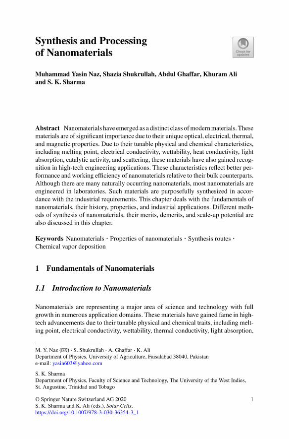
Water is a good microwave absorber and a polar solvent. Figure 7 shows a sim-plified schematic illustration of heating mechanism of the water molecules throughmicrowaves [23]. Polarized water molecules attempt to orientate during microwave
14 M. Y. Naz et al.
Fig. 7 Water molecules under microwave irradiation in an alternating electric field
heating with the quickly changing alternating electric field. In response, heat pro-duces due to the rotation, collision, and friction of the water molecules. When ionicsalts are dissolved in water, they affect the structure of the water molecules. Therelaxation time of the molecules at lower concentrations initially reduces and thenrises. The presence of the ions is assumed to cause a breakage of the hydrogen bond-ing in water. Those water molecules that are aligned with the ions are relatively fixed,but those that are not coordinated do not experience such powerful intermolecularhydrogen-bonding impacts, and thus have reduced relaxation times in this free state.The impacts are reversed at higher concentrations and the relaxation time of waterin concentrated salt solutions is higher than that of pure water, probably owing toa higher ordering of water molecules when there is a large amount of ions in thesolution.
The metallic nanomaterials of different morphologies, including nanospheres,nanopolygonal plates, nanosheets, nanorods, nanowires, nanotubes, etc. can be pre-pared within few minutes through microwave heating. The morphology and size ofnanostructures can be regulated by changing multiple experimental parameters suchas metal salt concentration, surfactant chain length, solvent, and temperature of thereaction.
3.5 Plasma Synthesis Technique
Different kinds of plasma reactors that can be used to synthesize nanocrystals have anumber of common characteristics to help understand suitable conditions for plasmaformation and growth of nanocrystals. The main characteristics are:
• Reactor vessel: It describes the plasma volume and separates the mixture ofprecursor gases (often diluted in an inert carrier gas) from the surrounding air.

Synthesis and Processing of Nanomaterials 15
• Electrical power: An electric power supply is used to convert the gas mixture intoplasma through direct current electric field or time-varying radio or microwavefrequencies.
• Plasma electrodes: These are the means of plasma coupling such as electrodes,resonant cavities, or antennas.
• Gas controllers: Such devices are attached to the plasma reactors for controllingthe supply of precursor gases or vapors and to create the desired gas pressure inthe plasma reactor [18].
In low-pressure plasmas, two distinct types of synthesis strategies are adopted:batch reactors and flow-through reactors. The performance of batch type reactorsdepends on ability of the discharge plasmas to trap the negatively charged speciesproduced during gas ionization. The charged species may be subjected to a constantflow of gases and allowed to expand to larger dimensions. Particles are gathered afterswitching off the plasma and enabling the particles to drop down on a substratum bygravity or through the gas flow to a filter. In a flow-through reactor, nanoparticles aretransported through the reactor in a gas flow soon after they nucleate and develop.As the nanoparticles grow, the precursor will be depleted and particle growth willultimately be limited in the gas streamby the available precursor. Particles are broughtinto the gas that flows out of the reactor and gathered on a substratum or using filters[21].
3.6 Simple Heating Method
The easiest way to produce the nanoparticles is to heat the precursor material in aheat-resistant crucible. Figure 8 shows a schematic representation of the gas phasesynthesis method of single-phase nanomaterials from a heated crucible [4]. Thismethod is only suitable for materials with high vapor pressure at temperatures ofup to 2000 °C. The energy is supplied to the precursor material through arc heating,Joule heating, or electron-beam heating. The atoms evaporate into an atmosphere thatis either inert or reactive (so that a compound is formed). In order to perform reactivesynthesis, materials with very low vapor pressure must be fed into the furnace in theform of an appropriate precursor such as organometallics, which decomposes intothe furnace to produce a condensable material. The atoms of the evaporated materiallose energy by collision with the cold gas atoms and undergo condensation throughhomogeneous nucleation into tiny clusters. The precursors react in the gas phasewhen a compound material is synthesized. The precursors form a compound withthe material that is injected independently into the reaction chamber. If they remainin a supersaturated region, the clusters would continue to grow. To control their size,a carrier gas is used to remove them quickly from the supersaturated environment.Three parameters play a key role in controlling the cluster size and its distribution:
i. Evaporation rate, which depends on energy input.ii. Condensation rate, which depends on energy removal.

16 M. Y. Naz et al.
Fig. 8 Schematicrepresentation of the gasphase synthesis method forsingle-phase nanomaterialsfrom a heated crucible
iii. Gas flowrate, which for removal of clusters.
This method can be extended from laboratory to industrial scale due to its inherentsimplicity [4].
3.7 Solvent Evaporation Technique
The first technique established for the preparing of nanoparticles was solvent evapo-ration. Using this technique, polymer solutions were formed in volatile solvents andemulsions were formulated with the use of dichloromethane and chloroform. Nowa-days, ethyl acetate is preferred for the stated purpose due to its better toxicologicalprofile for obtaining the polymeric particles with dimensions smaller than 500 nm.During the preparation stage, the emulsion is transformed into a nanoparticular sus-pension when the solvent is evaporated, after which the solution can be diffusedthrough the continuous emulsion phase by performing some standard procedures.The procedures involve high-speed ultrasonication or homogenization and evapora-tion of the solvent through magnetic stirring at room temperature or under reducedpressure. The magnetic stirring results in solidified nanosized particles, which arecollected through ultracentrifugation and washed to remove surfactants. Finally, theproduct is lyophilized [24] (Fig. 9).
This technique comprises of the preparing of nanoemulsions, formulated in avolatile solvent solution with a polymer dissolved. Dichloromethane and chloroformare the commonly used solvents, but are often substituted by ethyl acetate, a less toxicsolvent, and therefore much more suited to the synthesis of the controlled releasesystems in which the encapsulation of drugs is involved. This technique is performedunder vacuum where suspension is developed by evaporating polymer solvent from

Synthesis and Processing of Nanomaterials 17
Fig. 9 Illustration of a solvent evaporation technique
emulsion droplets, which can be diffused through the continuous phase. This slowmethod includes a rapid evaporation period in which at least 90% of the remainingsolvent is removed, followed by a slow evaporation period in which the remainingsolvent is extracted.Due to the elevated solvent loss, droplet size dramatically reducesduring the first step to reach a minimum value. On the contrary, a substantial rise indroplet diameter due to coalescence characterizes the second step. In polymers withinterfacial adsorption characteristics, this coalescence process can be accentuated,whereas in polymers with bad surface-active characteristics, coalescence is low.Furthermore, partly miscible solvents can be used in emulsion precipitation andevaporation conditions can be changed. In this case, the removal of volatile solventscan be done by distillation [25].
3.8 Mechanochemical Process
Mechanical attrition is a technique established in 1970 to produce fresh alloys andphase mixtures from powder particles as an industrial process. The quantity limita-tions for nanocrystalline preparation can possible be controlled through this tech-nique; therefore, nanocrystalline powders can be produced on large scale. It alsoprovides many options in the preparation of various structures in nanostructuredpowders such as crystalline–crystalline or amorphous–crystalline and atomic bond-ing like metal–metal, metal–semiconductor, and metal–ceramic materials. The mostsignificant benefit is that mechanical milling can be performed at lower temperatures,allowing the newly shaped grains to grow very slowly [6]. The highmechanical forceleads to the destruction of materials and creates a distinct structure. Mechanochem-ical technique has been commonly used in advanced material synthesis, coveringnearly all aspects of material science.

18 M. Y. Naz et al.
Planetary ball mill is a typical mechanical process whereby the planetary ballmill is used for grinding of the materials by rotating the big plate continuously andsimultaneously rotating the containers. The speed of the plate revolution and thespeed of the container rotation can be adjusted independently [26]. Particles largerthan 100 nm cannot, therefore, be excessively cold welded. As a consequence, theaverage grain size can be reduced by up to 2–20 nm. The mechanism of formationof microstructure is very distinct from other techniques of synthesis, but it is verycomparable to the final microstructure. Due to mechanical attrition, a severe plasticdeformation happens, resulting in a constant refinement of the inner composition ofthe powder particles to nanometer scale [27].
Mechanical milling is susceptible to contamination; it is possible to use atmo-spheric control for chemical reactions between atmosphere and milled powders.This has resulted in a novel and cost-effective technique for production of nanopow-ders. A conventional ball mill can be used as a chemical reactor at low temperaturesfor mechanochemical processing. Ball milling improves the reaction kinetics of thereactants due to intimate mixing and refinement of grain structure to nanometerscale. Since reaction takes place during actual milling, a suitable reactive gas (oxy-gen or nitrogen, atmospheric air) and a suitable precursor are used during millingstage. A variety of metals can be used in reactive milling where metal powders aretransformed to nanocrystalline metal–ceramic composites [6]. Reducing the processcost and product industrialization can be achieved using a variety of precursors suchas carbonates, fluorides, oxides, hydroxides, sulfates, chlorides, etc. For mechani-cal attrition, various ball mills such as tumbler mills, shaker mills, planetary mills,vibratory mills, etc. have been developed. The material powder is put in a sealedcontainer with tungsten carbide or steel coated balls. Kinetic energy of balls dependson their mass and velocity. Since steel or tungsten is high-density materials, they arepreferred as a milling material [6].
3.9 Sonochemical Technique
Sonochemistry is a technique in which the application of strong ultrasound radia-tion causes molecules to undergo a chemical reaction. Acoustic cavitation, whichinvolves the formation, growth, and fall of bubbles in an ultrasonically irradiatedliquid, is the driving force responsible for the sonochemical process. Although in theconstruction of reactors cavitation is prevented, still acoustic cavitation is the key tosonochemical processing owing to its capacity to regulate and restrict its impacts tothe reaction rather than the reactor. This technique has been used widely to createextraordinary characteristics of nanosized materials. Unique process conditions suchas elevated temperature, elevated pressure, and elevated cooling rates make it easierto form smaller particles and different product sizes compared to other techniques.In conducting sonochemical experiments, the primary benefit is that it is very cheap[6].

Synthesis and Processing of Nanomaterials 19
Fig. 10 Schematic of a chemical vapor deposition reactor
3.10 Chemical Vapor Deposition Technique
Chemical vapor deposition (CVD) is referred to as activating chemical reactionsbetween a substrate surface and a gaseous precursor in order to deposit a thin solidfilm onto the substrate. Surface activation and growth activity can be achieved eitherwith increased temperatures (thermalCVD)orwith plasma (plasma-enhancedCVD).A PECVD process is carried out at significantly lower temperatures compared to thethermal CVD process [6]. CVD is a widely used technique in material processingindustry due to its low set-up cost, high production yield, and ease of scale-up. Asshown in Fig. 10, CVD has been developed as a novel manufacturing process inmany industrial sectors such as semiconductors and ceramic industry [28].
A typical CVD process involves the mass transportation of reactants delivered bythe gaseous or liquid precursor to the substrate surface, adsorption of reactants atsubstrate surface, chemical reaction of the reactants at the substrate surface to formthinfilm, desorptionof by-products of the reaction fromsubstrate surface and removalof by-products and unreacted reactants. The deposition rate of a film in CVD processis mainly controlled by the slowest step in this serial process [16]. Since adsorptionand desorption at the substrate surface usually occur at relatively faster rates, thedeposition rate is anticipated from the competition between mass transportation ofreactants in the first step, by-products in the last step, and the surface reaction ratein the third step. The whole process is illustrated in Fig. 11. Mass transportation isa function of gas flowrate and its partial pressure while surface reaction rate is anexponential function of process temperature [16].

20 M. Y. Naz et al.
Fig. 11 Illustration of a typical CVD process involving five growth steps
The chemical response of the surface is dominant at elevated temperatures. Assoon as it hits the surface, the precursor will react with the substrate and form athin film. Therefore, mass transportation controls this process. By raising the supplyof reactants such as gas or liquid precursors, mass transportation can be improvedand consequently the rate of deposition. Usually, the deposition occurs at variousnucleation sites and expands and coalesces together.
Since deposition rate is governed by the mass transportation, if the surface hasa pronounced topography, the film tends not to be conformal and the depositionrate is also usually difficult to control. On the other side, the surface reaction rate isslow for a low-temperature regime and becomes the dominant phase. In this case,the deposition rate will remain the same regardless of any change in the flowrateof reactants. The surface will have an adequate supply of reactants due to the slowreaction rate, and reactions generally occur concurrently in all surface fields, resultingin a very uniformand conformal deposition.However, if the temperature is too low forthermodynamic reasons, the reaction may not happen at all. It reveals that for a CVDmethod, selecting the right temperature is of significant importance.
CVD reactors are classified into normal CVD reactors and PECVD reactors. In anormal CVD process, reactants can be either gases or liquids and there can be morethan one reactant. The reactant generally has a thermal decomposition reaction atthe surface of the substrate if there is only one reactant involved in a CVD process.If more than one reactant is involved, these would be the precursor and a reducingagent. The normal CVD reaction temperature varies from case to case; however, itshould be high enough to initiate the decomposition of the precursors and activationof the substrate surface [16].
Like a PVD method, DC or RF plasma is also used in many modern thin-filmdeposition methods involving CVD reactors. The plasma helps in breaking down theprecursors before they reach the surface of the substrate. Therefore, it considerably

Synthesis and Processing of Nanomaterials 21
reduces the surface temperature needed for the chemical reactions. The plasmas aregenerated and sustained under very low pressures [16].
A typical CVD reactor includes gas delivery system, loading/unloading sys-tem, reaction chamber, vacuum system, energy system, process control system, andexhaust gas treatment system. The gases are fed into the reaction chamber at temper-atures in the range of 500–1200°C. Other than the precursor gas, argon and nitrogenare used as carrier gases. When gases come into contact with the heated substratein the reactor they react and form a strong layer on the surface of the substrate.The critical operating parameters of this method are the temperature and workingpressure [6]. Finally, CVD is being widely used for synthesis of carbon nanotubesand is the most promising technique as compared to arc discharge and laser abla-tion techniques. Recently, a swirled floating catalyst CVD reactor is developed forup-scaling nanotubes’ production capacity. A vertical reactor was placed inside afurnace and cyclones for collecting the final product [6]. It is worth mentioning thatalthough CVD is a flexible technique, it requires numerous experimental works forstandardization of the appropriate growth parameters [6].
4 Applications of Nanomaterials
Nanotechnology is being implemented through a range of applications from opti-cal communications, electronics, biological systems, and automotive engineeringto new materials. Many possible applications have been explored and a number ofnanomaterials’-based devices and systems have been studied previously [29, 30, 36,37]. These applications are based on (i) the peculiar physical properties of nanosizedmaterials, for example, gold nanoparticles used as inorganic dye to introduce colorsinto glass and as low-temperature catalyst, (ii) the huge surface area, such as meso-porous titania for photo-electrochemical cells, and nanoparticles for various sensors,and (iii) the small size that offers extra possibilities for manipulation and room foraccommodating multiple functionalities [5]. Future applications of nanomaterialsinclude next era laptop chips, better insulation materials, kinetic power penetrators,lethal weapons, phosphors for high definition televisions, low cost flat panel display,cutting tools, pollution remediation, high-density materials, powerful magnets, highperformance batteries, highly sensitive sensors, aerospace additives with superiorperformance, advanced weapon platforms, satellites, medical implants, machinableceramics, drug delivery, smart buildings, etc.