rz/a2m group application note example of booting from ... · rz/a2m group example of booting from...
TRANSCRIPT
APPLICATION NOTE
R01AN4333EJ0100 Rev.1.00 Page 1 of 86 Dec. 18, 2018
RZ/A2M Group Example of Booting from Serial Flash Memory Abstract This application note describes an example of booting from the serial flash memory via the SPI multi-I/O bus controller (hereinafter called "SPIBSC") of RZ/A2M by using the boot mode 3 (serial flash boot 3.3V) function.
Products RZ/A2M
When using this application note with other Renesas MCUs, careful evaluation is recommended after making modifications to comply with the alternate MCU.
R01AN4333EJ0100 Rev.1.00
Dec. 18, 2018

RZ/A2M Group Example of Booting from Serial Flash Memory
R01AN4333EJ0100 Rev.1.00 Page 2 of 86 Dec. 18, 2018
Contents
1. Specifications ................................................................................................................. 4 1.1 Booting from Serial Flash Memory ........................................................................................... 4 1.2 Peripheral Functions Used ......................................................................................................... 6
2. Operation Confirmation Conditions .............................................................................. 7
3. Reference Application Notes ......................................................................................... 8
4. Hardware ......................................................................................................................... 9 4.1 Hardware Configuration ............................................................................................................. 9 4.2 Pins Used ................................................................................................................................... 10
5. Software ........................................................................................................................ 11 5.1 Operation Overview .................................................................................................................. 11
5.1.1 Terms Related to Serial Flash Boot .................................................................................. 11 5.1.2 Operation Overview of Sample Code Overall .................................................................. 12 5.1.3 Operation Overview of Loader Program ........................................................................... 13 5.1.4 Application Program ........................................................................................................... 17
5.2 Peripheral Functions and Memory Allocation in Sample Code ........................................... 19 5.2.1 Setting for Peripheral Functions ....................................................................................... 19 5.2.2 Memory Mapping................................................................................................................. 20 5.2.3 Section Assignment in Sample Code ............................................................................... 21
5.3 Interrupt Used ............................................................................................................................ 22 5.4 Data Types ................................................................................................................................. 22 5.5 Constants Used by the Loader Program ................................................................................ 23 5.6 List of Structures/Unions Used by the Loader Program ....................................................... 25 5.7 List of Variables for Loader Program ...................................................................................... 37 5.8 List of Functions Used in the Loader Program ...................................................................... 38 5.9 Function Specification .............................................................................................................. 40 5.10 Loader Program Flowcharts .................................................................................................... 46
5.10.1 Loader program (overall) ................................................................................................... 46 5.10.2 SPIBSC and Serial Flash Memory Initial Setting ............................................................. 47 5.10.3 SPIBSC Initial Setting ......................................................................................................... 49 5.10.4 SPIBSC Operating Mode Setting ....................................................................................... 51 5.10.5 Issuance of SPI Command to Serial Flash Memory ........................................................ 54 5.10.6 SPIBSC Read Timing Calibration for DDR Transfer ........................................................ 58
6. Application Example .................................................................................................... 62 6.1 Operation of the Sample Code Used in its Initial State ......................................................... 62 6.2 Changing the Sample Code When Not Changing the Serial Flash Memory ....................... 66
6.2.1 Changing to SDR Transfer Read Command .................................................................... 66 6.3 Changing the Sample Code When Changing the Serial Flash Memory .............................. 68
RZ/A2M Group Example of Booting from Serial Flash Memory
R01AN4333EJ0100 Rev.1.00 Page 3 of 86 Dec. 18, 2018
6.3.1 Signal Output when a Read Command is Issued ............................................................ 70 6.3.2 Setting up the Serial Flash Memory Registers ................................................................ 74 6.3.3 Serial Flash Memory Write Completion Wait ................................................................... 75 6.3.4 Serial Flash Memory Status Register Read ...................................................................... 76 6.3.5 Serial Flash Memory Configuration Register Read ......................................................... 78 6.3.6 Serial Flash Memory Write Enable .................................................................................... 80 6.3.7 Serial Flash Memory Status/Configuration Register Write ............................................. 82
7. Sample Code Precautions ........................................................................................... 84 7.1 Accessible area in external address space read mode ........................................................ 84
8. Sample Code ................................................................................................................ 85
9. Reference Documents .................................................................................................. 85

RZ/A2M Group Example of Booting from Serial Flash Memory
R01AN4333EJ0100 Rev.1.00 Page 4 of 86 Dec. 18, 2018
1. Specifications 1.1 Booting from Serial Flash Memory In boot mode 3, the RZ/A2M boots from the serial flash memory allocated to the SPI multi-I/O bus space (hereinafter called "serial flash boot"). Figure 1.1 shows the Conceptual diagram of serial flash boot operation.
Figure 1.1 Conceptual diagram of serial flash boot operation
The conceptual diagram of serial flash boot operation is described below.
1 When the RZ/A2M starts up by serial flash boot, the boot startup on-chip ROM program runs after power-on reset is canceled.
2 The boot startup on-chip ROM program sets the SPIBSC to external address space read mode to enable to directly run programs allocated to the SPI multi-I/O bus space.
3 The serial flash memory initial settings are made. 4 The loader program is transferred from the serial flash memory to the large-capacity on-chip RAM. 5 Execution branches to the start address of the loader program, which has been transferred to the large-capacity on-
chip RAM. 6 The loader program changes the SPIBSC settings. 7 The loader program changes the serial flash memory settings. 8 Execution branches to the start address of the application program.
Loader program
RZ/A2M
Boot startupon-chip ROM program
Boot startup on-chip ROM
Large-capacity on-chip RAM
SPI multi-I/Obus controller(SPIBSC)
Serial flash memory
4. Transfer to large-capacity on-chip RAM
5. Branch to start of loader program
2. Enable SPIBSC(pin settings and release of module standby)
3. Serial flash memory initial setting
1. Execute boot startup on-chip ROM program
Loader program
6. Change SPIBSC settings
7. Change serial flash memory settings
(Quad operation setting and 4-byte addressing settings)
8. Branch to start of application program
Applicationprogram
(User program)

RZ/A2M Group Example of Booting from Serial Flash Memory
R01AN4333EJ0100 Rev.1.00 Page 5 of 86 Dec. 18, 2018
The boot startup on-chip ROM program makes settings to allow common access to typical serial flash memory devices, so it is necessary to provide the optimal settings to the serial flash memory used by the customer. For the purpose of this setting, this application note describes how to allocate the loader program which provides optimal settings to the serial flash memory used by the customer to the start address (H'2000_0000) of the SPI multi-I/O bus space branched by the boot startup on-chip ROM program, and then branch to the customer-created application program (user program) after optimal settings are provided by the loader program.
This application provides a method for providing optimal settings to the serial flash memory used by the customer using the loader program and a method for creating the application program (user program).
RZ/A2M Group Example of Booting from Serial Flash Memory
R01AN4333EJ0100 Rev.1.00 Page 6 of 86 Dec. 18, 2018
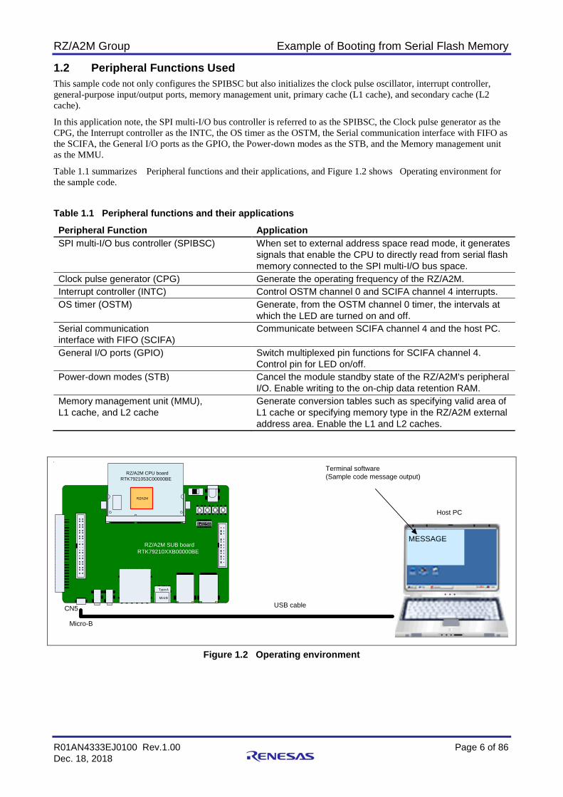
1.2 Peripheral Functions Used This sample code not only configures the SPIBSC but also initializes the clock pulse oscillator, interrupt controller, general-purpose input/output ports, memory management unit, primary cache (L1 cache), and secondary cache (L2 cache).
In this application note, the SPI multi-I/O bus controller is referred to as the SPIBSC, the Clock pulse generator as the CPG, the Interrupt controller as the INTC, the OS timer as the OSTM, the Serial communication interface with FIFO as the SCIFA, the General I/O ports as the GPIO, the Power-down modes as the STB, and the Memory management unit as the MMU.
Table 1.1 summarizes Peripheral functions and their applications, and Figure 1.2 shows Operating environment for the sample code.
Table 1.1 Peripheral functions and their applications
Peripheral Function Application SPI multi-I/O bus controller (SPIBSC) When set to external address space read mode, it generates
signals that enable the CPU to directly read from serial flash memory connected to the SPI multi-I/O bus space.
Clock pulse generator (CPG) Generate the operating frequency of the RZ/A2M. Interrupt controller (INTC) Control OSTM channel 0 and SCIFA channel 4 interrupts. OS timer (OSTM) Generate, from the OSTM channel 0 timer, the intervals at
which the LED are turned on and off. Serial communication interface with FIFO (SCIFA)
Communicate between SCIFA channel 4 and the host PC.
General I/O ports (GPIO) Switch multiplexed pin functions for SCIFA channel 4. Control pin for LED on/off.
Power-down modes (STB) Cancel the module standby state of the RZ/A2M's peripheral I/O. Enable writing to the on-chip data retention RAM.
Memory management unit (MMU), L1 cache, and L2 cache
Generate conversion tables such as specifying valid area of L1 cache or specifying memory type in the RZ/A2M external address area. Enable the L1 and L2 caches.
Figure 1.2 Operating environment
MESSAGE
Host PC
USB cable
Terminal software(Sample code message output)
Micro-B
CN5
NANDU32
ON
1 2 3 4 5 6 7 8 9 10
LVDSCN14
Backlight
CN16
RZ/A2M CPU boardRTK7921053C00000BE
RZ/A2M
RZ/A2M SUB boardRTK79210XXB00000BE
Mini-B
Type-A
RZ/A2M Group Example of Booting from Serial Flash Memory
R01AN4333EJ0100 Rev.1.00 Page 7 of 86 Dec. 18, 2018
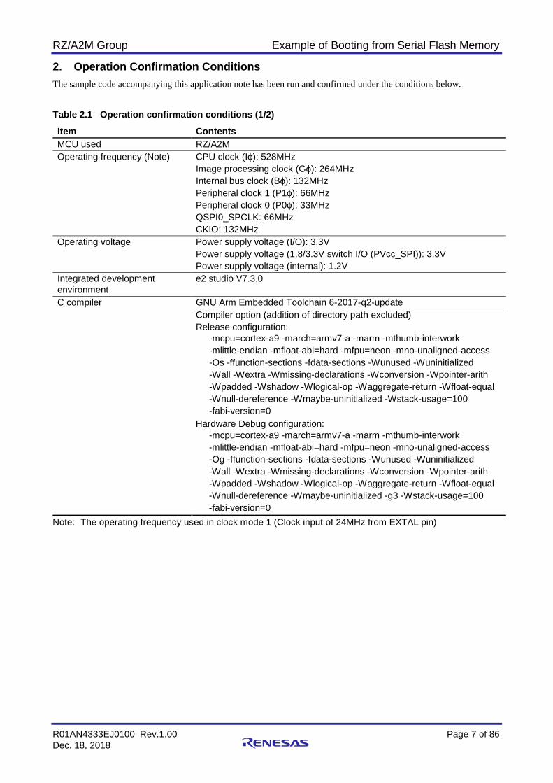
2. Operation Confirmation Conditions The sample code accompanying this application note has been run and confirmed under the conditions below.
Table 2.1 Operation confirmation conditions (1/2)
Item Contents MCU used RZ/A2M Operating frequency (Note) CPU clock (Iϕ): 528MHz
Image processing clock (Gϕ): 264MHz Internal bus clock (Bϕ): 132MHz Peripheral clock 1 (P1ϕ): 66MHz Peripheral clock 0 (P0ϕ): 33MHz QSPI0_SPCLK: 66MHz CKIO: 132MHz
Operating voltage Power supply voltage (I/O): 3.3V Power supply voltage (1.8/3.3V switch I/O (PVcc_SPI)): 3.3V Power supply voltage (internal): 1.2V
Integrated development environment
e2 studio V7.3.0
C compiler GNU Arm Embedded Toolchain 6-2017-q2-update Compiler option (addition of directory path excluded) Release configuration:
-mcpu=cortex-a9 -march=armv7-a -marm -mthumb-interwork -mlittle-endian -mfloat-abi=hard -mfpu=neon -mno-unaligned-access -Os -ffunction-sections -fdata-sections -Wunused -Wuninitialized -Wall -Wextra -Wmissing-declarations -Wconversion -Wpointer-arith -Wpadded -Wshadow -Wlogical-op -Waggregate-return -Wfloat-equal -Wnull-dereference -Wmaybe-uninitialized -Wstack-usage=100 -fabi-version=0
Hardware Debug configuration: -mcpu=cortex-a9 -march=armv7-a -marm -mthumb-interwork -mlittle-endian -mfloat-abi=hard -mfpu=neon -mno-unaligned-access -Og -ffunction-sections -fdata-sections -Wunused -Wuninitialized -Wall -Wextra -Wmissing-declarations -Wconversion -Wpointer-arith -Wpadded -Wshadow -Wlogical-op -Waggregate-return -Wfloat-equal -Wnull-dereference -Wmaybe-uninitialized -g3 -Wstack-usage=100 -fabi-version=0
Note: The operating frequency used in clock mode 1 (Clock input of 24MHz from EXTAL pin)
RZ/A2M Group Example of Booting from Serial Flash Memory
R01AN4333EJ0100 Rev.1.00 Page 8 of 86 Dec. 18, 2018
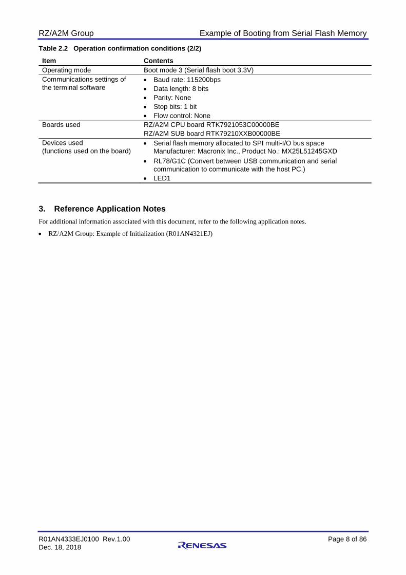
Table 2.2 Operation confirmation conditions (2/2)
Item Contents Operating mode Boot mode 3 (Serial flash boot 3.3V) Communications settings of the terminal software
• Baud rate: 115200bps • Data length: 8 bits • Parity: None • Stop bits: 1 bit • Flow control: None
Boards used RZ/A2M CPU board RTK7921053C00000BE RZ/A2M SUB board RTK79210XXB00000BE
Devices used (functions used on the board)
• Serial flash memory allocated to SPI multi-I/O bus space Manufacturer: Macronix Inc., Product No.: MX25L51245GXD
• RL78/G1C (Convert between USB communication and serial communication to communicate with the host PC.)
• LED1
3. Reference Application Notes For additional information associated with this document, refer to the following application notes.
• RZ/A2M Group: Example of Initialization (R01AN4321EJ)

RZ/A2M Group Example of Booting from Serial Flash Memory
R01AN4333EJ0100 Rev.1.00 Page 9 of 86 Dec. 18, 2018
4. Hardware 4.1 Hardware Configuration In the serial flash boot example introduced in this application note, processing is performed by the programs stored in the serial flash memory connected to the SPI multi-I/O bus space using boot mode 3. Figure 4.1 shows the Connection example for booting from serial flash memory in boot mode 3.
Note: # is a symbol that indicates negative logic (or active low).
Figure 4.1 Connection example for booting from serial flash memory in boot mode 3
3.3V
3.3V
3.3V
3.3V
3.3V
RZ/A2MSerial flash memory
MX25L51245GXD
CS#
SCLKQSPI0_SPCLK
RPC_RESET# RESET# VCC
QSPI0_SSL
SI/SIO0QSPI0_IO0
MD_BOOT1
MD_BOOT0
Boot mode 3
MD_BOOT2
PVcc_SPI
SO/SIO1
WP#/SIO2
NC/SIO3
QSPI0_IO1
QSPI0_IO2
QSPI0_IO3
3.3V
3.3V
3.3V
3.3V
3.3V
RZ/A2M Group Example of Booting from Serial Flash Memory
R01AN4333EJ0100 Rev.1.00 Page 10 of 86 Dec. 18, 2018
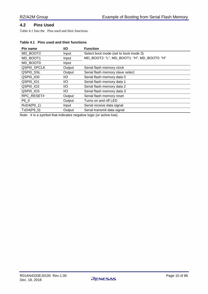
4.2 Pins Used Table 4.1 lists the Pins used and their functions.
Table 4.1 Pins used and their functions
Pin name I/O Function MD_BOOT2 Input Select boot mode (set to boot mode 3)
MD_BOOT2: "L", MD_BOOT1: "H", MD_BOOT0: "H" MD_BOOT1 Input MD_BOOT0 Input QSPI0_SPCLK Output Serial flash memory clock QSPI0_SSL Output Serial flash memory slave select QSPI0_IO0 I/O Serial flash memory data 0 QSPI0_IO1 I/O Serial flash memory data 1 QSPI0_IO2 I/O Serial flash memory data 2 QSPI0_IO3 I/O Serial flash memory data 3 RPC_RESET# Output Serial flash memory reset P6_0 Output Turns on and off LED RxD4(P9_1) Input Serial receive data signal TxD4(P9_0) Output Serial transmit data signal
Note: # is a symbol that indicates negative logic (or active low).
RZ/A2M Group Example of Booting from Serial Flash Memory
R01AN4333EJ0100 Rev.1.00 Page 11 of 86 Dec. 18, 2018
5. Software 5.1 Operation Overview This section provides an overview of the sample code operation presented in this application note.
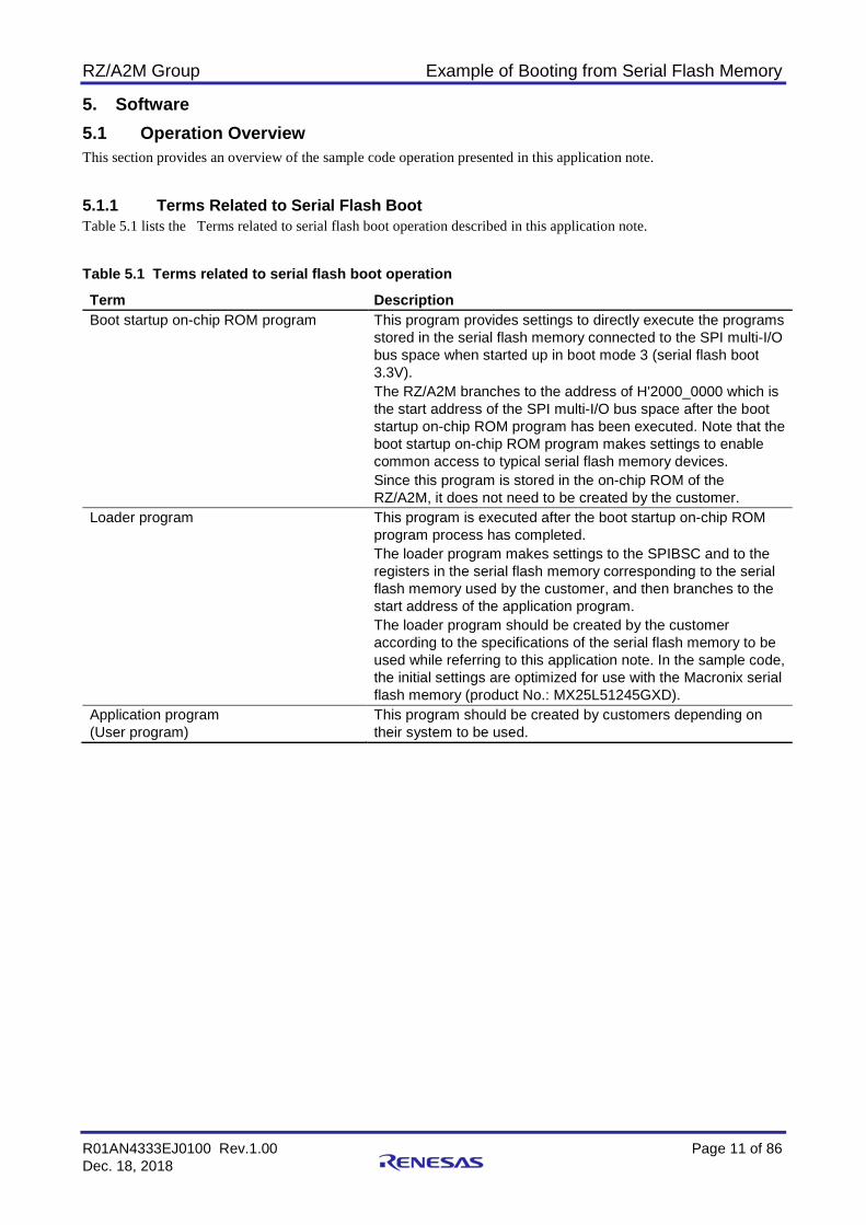
5.1.1 Terms Related to Serial Flash Boot Table 5.1 lists the Terms related to serial flash boot operation described in this application note.
Table 5.1 Terms related to serial flash boot operation
Term Description Boot startup on-chip ROM program This program provides settings to directly execute the programs
stored in the serial flash memory connected to the SPI multi-I/O bus space when started up in boot mode 3 (serial flash boot 3.3V). The RZ/A2M branches to the address of H'2000_0000 which is the start address of the SPI multi-I/O bus space after the boot startup on-chip ROM program has been executed. Note that the boot startup on-chip ROM program makes settings to enable common access to typical serial flash memory devices. Since this program is stored in the on-chip ROM of the RZ/A2M, it does not need to be created by the customer.
Loader program This program is executed after the boot startup on-chip ROM program process has completed. The loader program makes settings to the SPIBSC and to the registers in the serial flash memory corresponding to the serial flash memory used by the customer, and then branches to the start address of the application program. The loader program should be created by the customer according to the specifications of the serial flash memory to be used while referring to this application note. In the sample code, the initial settings are optimized for use with the Macronix serial flash memory (product No.: MX25L51245GXD).
Application program (User program)
This program should be created by customers depending on their system to be used.
RZ/A2M Group Example of Booting from Serial Flash Memory
R01AN4333EJ0100 Rev.1.00 Page 12 of 86 Dec. 18, 2018
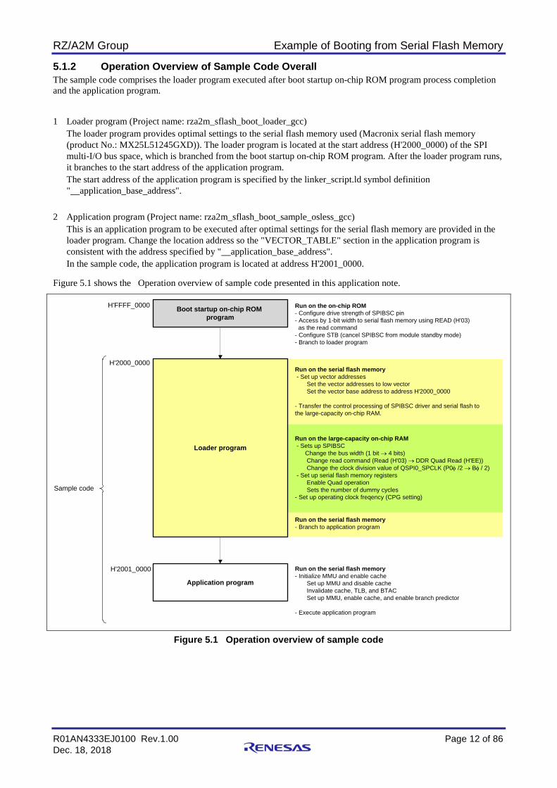
5.1.2 Operation Overview of Sample Code Overall The sample code comprises the loader program executed after boot startup on-chip ROM program process completion and the application program.
1 Loader program (Project name: rza2m_sflash_boot_loader_gcc)
The loader program provides optimal settings to the serial flash memory used (Macronix serial flash memory (product No.: MX25L51245GXD)). The loader program is located at the start address (H'2000_0000) of the SPI multi-I/O bus space, which is branched from the boot startup on-chip ROM program. After the loader program runs, it branches to the start address of the application program. The start address of the application program is specified by the linker_script.ld symbol definition "__application_base_address".
2 Application program (Project name: rza2m_sflash_boot_sample_osless_gcc)
This is an application program to be executed after optimal settings for the serial flash memory are provided in the loader program. Change the location address so the "VECTOR_TABLE" section in the application program is consistent with the address specified by "__application_base_address". In the sample code, the application program is located at address H'2001_0000.
Figure 5.1 shows the Operation overview of sample code presented in this application note.
Figure 5.1 Operation overview of sample code
Application program
Boot startup on-chip ROMprogram
H'2000_0000
H'2001_0000
H'FFFF_0000
Run on the serial flash memory- Set up vector addresses Set the vector addresses to low vector Set the vector base address to address H'2000_0000
- Transfer the control processing of SPIBSC driver and serial flash to the large-capacity on-chip RAM.
Run on the on-chip ROM- Configure drive strength of SPIBSC pin- Access by 1-bit width to serial flash memory using READ (H'03) as the read command- Configure STB (cancel SPIBSC from module standby mode)- Branch to loader program
Run on the serial flash memory- Initialize MMU and enable cache Set up MMU and disable cache Invalidate cache, TLB, and BTAC Set up MMU, enable cache, and enable branch predictor
- Execute application program
Sample code
Run on the large-capacity on-chip RAM- Sets up SPIBSC Change the bus width (1 bit → 4 bits) Change read command (Read (H'03) → DDR Quad Read (H'EE)) Change the clock division value of QSPI0_SPCLK (P0φ /2 → Bφ / 2) - Set up serial flash memory registers Enable Quad operation Sets the number of dummy cycles- Set up operating clock freqency (CPG setting)
Loader program
Run on the serial flash memory- Branch to application program

RZ/A2M Group Example of Booting from Serial Flash Memory
R01AN4333EJ0100 Rev.1.00 Page 13 of 86 Dec. 18, 2018
5.1.3 Operation Overview of Loader Program The loader program is executed after the boot startup on-chip ROM program process has completed. The loader program should be located at the start address (H'2000_0000) of the SPI multi-I/O bus space branched from the boot startup on-chip ROM program.
The boot startup on-chip ROM program makes settings to enable the SPIBSC to operate in external address space read mode. These settings cause the RZ/A2M to convert read operations targeting the SPI multi-I/O bus space to SPI communication so that the direct read operations are enabled to the connected serial flash memory. This makes it possible for the RZ/A2M to directly run programs allocated to the SPI multi-I/O bus space. The settings for commands targeting the serial flash memory used in SPI communication conversion allow common access to typical serial flash memory devices, so it is necessary to provide the optimal settings to the serial flash memory used by the customer.
The optimal settings for the serial flash memory are provided in two places: the registers in the SPIBSC module (hereinafter called "SPIBSC settings") and the registers in the serial flash memory (hereinafter called "serial flash memory settings").
In the loader program of the sample code, the data bus width is set to 4 bits, the transfer bit rate is optimized to the used read command, and the SPIBSC register is set to output a 4-byte address. Also, a Macronix serial flash memory (product No.: MX25L51245GXD) register is set to establish the number of serial flash memory dummy cycles, enable quad operations, and change to 4-byte addressing, and optimal settings are established to access MX25L51245GXD.
The process that establishes the loader program's SPIBSC settings and serial flash memory settings cannot be set by the program allocated to the SPI multi-I/O bus space, so these should be executed from the large-capacity on-chip RAM. In the sample code, the SPIBSC driver process and serial flash memory control process are transferred to the large-capacity on-chip RAM to be executed.
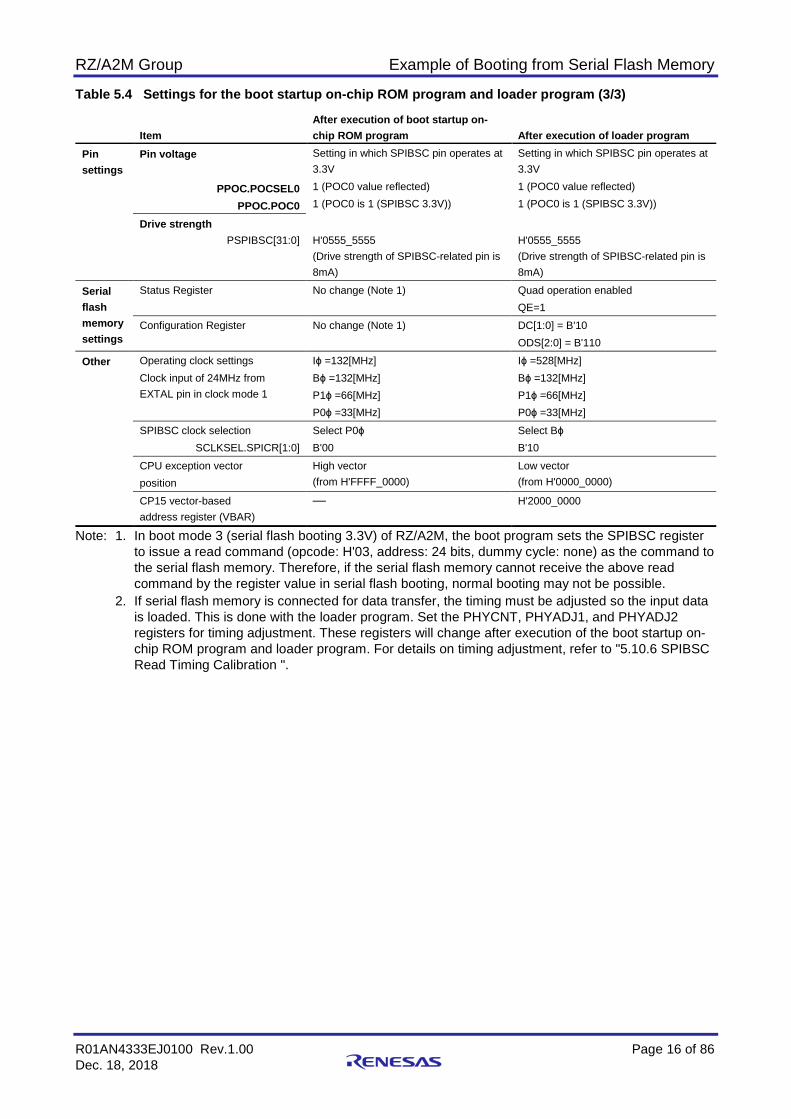
Refer to Table 5.2 to Table 5.4 for the settings after execution of the boot startup on-chip ROM program and loader program.
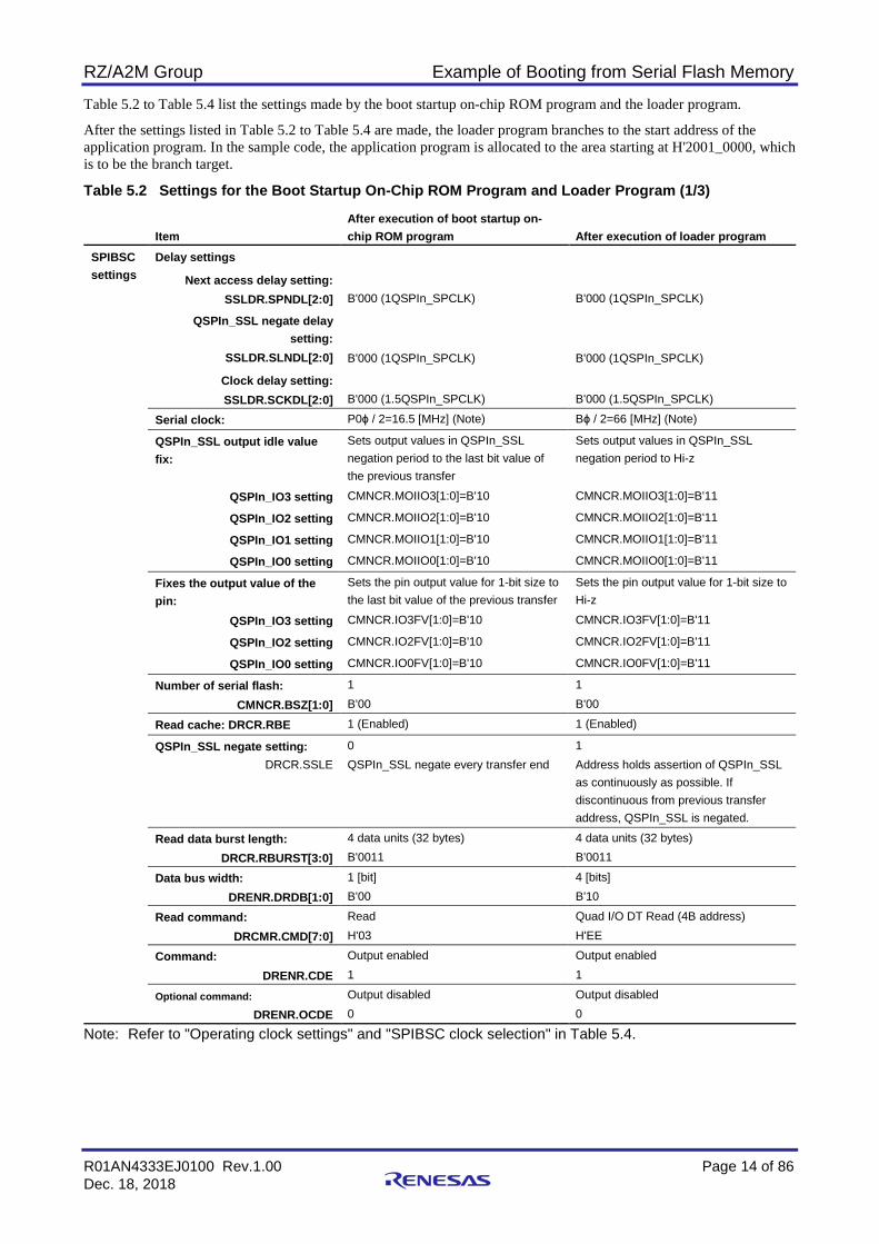
RZ/A2M Group Example of Booting from Serial Flash Memory
R01AN4333EJ0100 Rev.1.00 Page 14 of 86 Dec. 18, 2018
Table 5.2 to Table 5.4 list the settings made by the boot startup on-chip ROM program and the loader program.
After the settings listed in Table 5.2 to Table 5.4 are made, the loader program branches to the start address of the application program. In the sample code, the application program is allocated to the area starting at H'2001_0000, which is to be the branch target.
Table 5.2 Settings for the Boot Startup On-Chip ROM Program and Loader Program (1/3)
Item After execution of boot startup on-chip ROM program After execution of loader program
SPIBSC settings
Delay settings
Next access delay setting: SSLDR.SPNDL[2:0]
B'000 (1QSPIn_SPCLK)
B'000 (1QSPIn_SPCLK)
QSPIn_SSL negate delay setting:
SSLDR.SLNDL[2:0]
B'000 (1QSPIn_SPCLK)
B'000 (1QSPIn_SPCLK)
Clock delay setting: SSLDR.SCKDL[2:0]
B'000 (1.5QSPIn_SPCLK)
B'000 (1.5QSPIn_SPCLK)
Serial clock: P0ϕ / 2=16.5 [MHz] (Note) Bϕ / 2=66 [MHz] (Note)
QSPIn_SSL output idle value fix:
Sets output values in QSPIn_SSL negation period to the last bit value of the previous transfer
Sets output values in QSPIn_SSL negation period to Hi-z
QSPIn_IO3 setting CMNCR.MOIIO3[1:0]=B'10 CMNCR.MOIIO3[1:0]=B'11
QSPIn_IO2 setting CMNCR.MOIIO2[1:0]=B'10 CMNCR.MOIIO2[1:0]=B'11
QSPIn_IO1 setting CMNCR.MOIIO1[1:0]=B'10 CMNCR.MOIIO1[1:0]=B'11
QSPIn_IO0 setting CMNCR.MOIIO0[1:0]=B'10 CMNCR.MOIIO0[1:0]=B'11
Fixes the output value of the pin:
Sets the pin output value for 1-bit size to the last bit value of the previous transfer
Sets the pin output value for 1-bit size to Hi-z
QSPIn_IO3 setting CMNCR.IO3FV[1:0]=B'10 CMNCR.IO3FV[1:0]=B'11
QSPIn_IO2 setting CMNCR.IO2FV[1:0]=B'10 CMNCR.IO2FV[1:0]=B'11
QSPIn_IO0 setting CMNCR.IO0FV[1:0]=B'10 CMNCR.IO0FV[1:0]=B'11
Number of serial flash: CMNCR.BSZ[1:0]
1 B'00
1 B'00
Read cache: DRCR.RBE 1 (Enabled) 1 (Enabled)
QSPIn_SSL negate setting: DRCR.SSLE
0 QSPIn_SSL negate every transfer end
1 Address holds assertion of QSPIn_SSL as continuously as possible. If discontinuous from previous transfer address, QSPIn_SSL is negated.
Read data burst length: DRCR.RBURST[3:0]
4 data units (32 bytes) B'0011
4 data units (32 bytes) B'0011
Data bus width: DRENR.DRDB[1:0]
1 [bit] B'00
4 [bits] B'10
Read command: DRCMR.CMD[7:0]
Read H'03
Quad I/O DT Read (4B address) H'EE
Command: DRENR.CDE
Output enabled 1
Output enabled 1
Optional command:
DRENR.OCDE Output disabled 0
Output disabled 0
Note: Refer to "Operating clock settings" and "SPIBSC clock selection" in Table 5.4.

RZ/A2M Group Example of Booting from Serial Flash Memory
R01AN4333EJ0100 Rev.1.00 Page 15 of 86 Dec. 18, 2018
Table 5.3 Settings for the boot startup on-chip ROM program and loader program (2/3)
Item After execution of boot startup on-chip ROM program After execution of loader program
SPIBSC settings
Address enable: DRENR.ADE[3:0]
Output address [23:0] B'0111
Output address [31:0] B'1111
Address bit size: DRENR.ADB[1:0]
1 [bit] B'00
4 [bits] B'10
Option data enable: DRENR.OPDE[3:0]
Output disabled B'0000
Output OPD3 (Note) B'1000
Option data bit size: DRENR.OPDB[1:0]
— 4 [bits] B'10
Option data: DROPR.OPD3[7:0] DROPR.OPD2[7:0] DROPR.OPD1[7:0] DROPR.OPD0[7:0]
— — — —
H'00 — — —
Dummy cycle enable: DRENR.DME
Insertion disabled 0
Insertion enabled 1
Dummy cycle bit size: DRDMCR.DMDB[1:0]
— 1 [bit] B'00
Number of dummy cycles: DRDMCR.DMCYC[2:0]
— 7 cycles B'110
Extended address:
DREAR.EAC[2:0] DREAR.EAV[7:0]
External address bits [24:0] enabled Directly accessible 32MB spaces B'000 H'00
External address bits [27:0] enabled Directly accessible 256MB spaces B'011 H'00
Transfer format:
DRDRENR.HYPE[2:0] DRDRENR.ADDRE DRDRENR.OPDRE DRDRENR.DRDRE
PHYOFFSET1.DDTMG[1:0] PHYOFFSET2.OCTTMG[2:0]
Address, option data, and data are transferred in SDR mode, SPI flash mode B'000 0 0 0 B'11 (SDR) B'100 (Serial flash)
Address, option data, and data are transferred in DDR mode, SPI flash mode B'000 1 1 1 B'10 (DDR) B'100 (Serial flash)
OctaFlash backup alignment:
PHYCNT.ALT_ALIGN PHYCNT.OCTA[1:0]
Backup alignment during OctaFlash connection not supported. 0 B'00
Backup alignment during OctaFlash connection not supported. 0 B'00
OctaFlash protocol mode: PHYCNT.OCT
OctaFlash protocol not used 0
OctaFlash protocol not used 0
External data strobe: PHYCNT.EXDS
External data strobe signal not used 0
External data strobe signal not used 0
Device selection: PHYCNT.PHYMEM[1:0]
SDR mode serial flash B'00
DDR mode serial flash B'01
Note: The MX25L51245GXD transits to the Performance Enhance Mode when data (e.g., H'A5, H'5A, H'F0, H'0F, etc.) that toggles between bits 7-4 and bits 3-0 is input during the performance enhance indicator cycle that follows the address cycle. Since the RZ/A2M's external address space read mode does not support the data transfer in Performance Enhance Mode, the sample code makes configuration so that the MX25L51245GXD will not switch into the Performance Enhance Mode by making configuration so that H'00 is output from the OPD3 when a QuadIO DT Read command is issued.
RZ/A2M Group Example of Booting from Serial Flash Memory
R01AN4333EJ0100 Rev.1.00 Page 16 of 86 Dec. 18, 2018
Table 5.4 Settings for the boot startup on-chip ROM program and loader program (3/3)
Item After execution of boot startup on-chip ROM program After execution of loader program
Pin settings
Pin voltage
PPOC.POCSEL0 PPOC.POC0
Setting in which SPIBSC pin operates at 3.3V 1 (POC0 value reflected) 1 (POC0 is 1 (SPIBSC 3.3V))
Setting in which SPIBSC pin operates at 3.3V 1 (POC0 value reflected) 1 (POC0 is 1 (SPIBSC 3.3V))
Drive strength PSPIBSC[31:0]
H'0555_5555 (Drive strength of SPIBSC-related pin is 8mA)
H'0555_5555 (Drive strength of SPIBSC-related pin is 8mA)
Serial flash memory settings
Status Register No change (Note 1) Quad operation enabled QE=1
Configuration Register No change (Note 1) DC[1:0] = B'10 ODS[2:0] = B'110
Other Operating clock settings Clock input of 24MHz from EXTAL pin in clock mode 1
Iϕ =132[MHz] Bϕ =132[MHz] P1ϕ =66[MHz] P0ϕ =33[MHz]
Iϕ =528[MHz] Bϕ =132[MHz] P1ϕ =66[MHz] P0ϕ =33[MHz]
SPIBSC clock selection SCLKSEL.SPICR[1:0]
Select P0ϕ B'00
Select Bϕ B'10
CPU exception vector position
High vector (from H'FFFF_0000)
Low vector (from H'0000_0000)
CP15 vector-based address register (VBAR)
— H'2000_0000
Note: 1. In boot mode 3 (serial flash booting 3.3V) of RZ/A2M, the boot program sets the SPIBSC register to issue a read command (opcode: H'03, address: 24 bits, dummy cycle: none) as the command to the serial flash memory. Therefore, if the serial flash memory cannot receive the above read command by the register value in serial flash booting, normal booting may not be possible.
2. If serial flash memory is connected for data transfer, the timing must be adjusted so the input data is loaded. This is done with the loader program. Set the PHYCNT, PHYADJ1, and PHYADJ2 registers for timing adjustment. These registers will change after execution of the boot startup on-chip ROM program and loader program. For details on timing adjustment, refer to "5.10.6 SPIBSC Read Timing Calibration ".

RZ/A2M Group Example of Booting from Serial Flash Memory
R01AN4333EJ0100 Rev.1.00 Page 17 of 86 Dec. 18, 2018
5.1.4 Application Program (1) Operation of the application program
After a reset is cancelled, the boot startup on-chip ROM program and loader program are executed in that order. Then the execution transfers to the application program that is allocated to address H'2001_0000.
In the startup process, the settings for the stack pointer, MMU, and FPU are executed. The section initialization is performed, and it branches to the resetprg function.
In the resetprg function, after RTC and USB unused channel initialization processing is executed, L1 cache and L2 cache are enabled and INTC initialization is performed. The large-capacity on-chip RAM address is set in VBAR to enable high-speed interrupt processing, IRQ interrupt and FIQ interrupt are enabled, and the main function is called.
In the main function, CPG, OSTM channel 0, SCIFA channel 4, and GPIO initial setting processing is performed. As a result of this initialization processing, the main function outputs the character strings (startup message) to the terminal on the host PC connected with the serial interface and sets the OSTM channel 0 timer to interval timer mode to activate the timer. It generates the OSTM channel 0 interrupt with a cycle of 500ms and repeats turning on/off the LED on the CPU board every 500ms using such interrupt.
For details on the initialization executed by the application program, refer to the application note "RZ/A2M Group Example of Initialization".
RZ/A2M Group Example of Booting from Serial Flash Memory
R01AN4333EJ0100 Rev.1.00 Page 18 of 86 Dec. 18, 2018
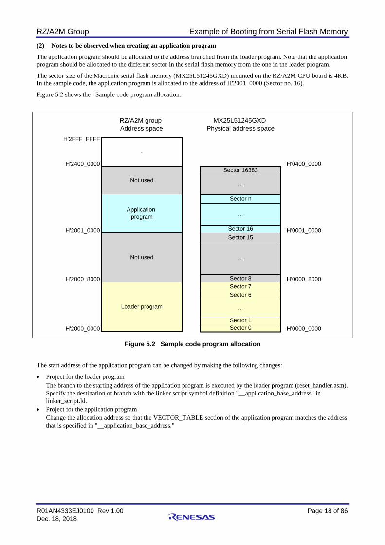
(2) Notes to be observed when creating an application program
The application program should be allocated to the address branched from the loader program. Note that the application program should be allocated to the different sector in the serial flash memory from the one in the loader program.
The sector size of the Macronix serial flash memory (MX25L51245GXD) mounted on the RZ/A2M CPU board is 4KB. In the sample code, the application program is allocated to the address of H'2001_0000 (Sector no. 16).
Figure 5.2 shows the Sample code program allocation.
Figure 5.2 Sample code program allocation
The start address of the application program can be changed by making the following changes:
• Project for the loader program The branch to the starting address of the application program is executed by the loader program (reset_handler.asm). Specify the destination of branch with the linker script symbol definition "__application_base_address" in linker_script.ld.
• Project for the application program Change the allocation address so that the VECTOR_TABLE section of the application program matches the address that is specified in "__application_base_address."
Loader program
Sector 0Sector 1
Sector 6Sector 7
Not used
Sector 16
...
Sector n
...
Sector 16383
Applicationprogram
Not used
RZ/A2M groupAddress space
MX25L51245GXDPhysical address space
H'0000_0000
H'0000_8000
H'0001_0000
H'0400_0000
H'2000_0000
H'2000_8000
H'2001_0000
H'2400_0000
...
Sector 8
Sector 15
...
-
H'2FFF_FFFF
RZ/A2M Group Example of Booting from Serial Flash Memory
R01AN4333EJ0100 Rev.1.00 Page 19 of 86 Dec. 18, 2018
5.2 Peripheral Functions and Memory Allocation in Sample Code 5.2.1 Setting for Peripheral Functions Table 5.5 lists the Setting for Peripheral Functions during execution of the sample code.
Table 5.5 Setting for Peripheral Functions
Module Settings CPG CPU clock: Set to 1/2 the PLL circuit frequency
Internal bus clock: Set to 1/8 the PLL circuit frequency Peripheral clock 1 (P1ϕ): Set to 1/16 the PLL circuit frequency If the input clock is 24MHz in clock mode 1 (divider 1: ×1/2, PLL circuit: ×88), set to the following frequencies • CPU clock (Iϕ): 528MHz • Image processing clock (Gϕ): 264MHz • Internal bus clock (Bϕ): 132MHz • Peripheral clock 1 (P1ϕ): 66MHz • Peripheral clock 0 (P0ϕ): 33MHz • QSPI0_SPCLK: 66MHz (when Bϕ is selected) • CKIO clock: 132MHz (when Bϕ is selected)
SPIBSC When set to the external address space read mode, it generates the signals which enable the CPU to read directly from the serial flash memory connected to the SPI multi-I/O bus space.
STB Writing to the on-chip RAM used for retention is enabled and clock supply to peripheral functions is enabled. Clock supply is enabled to OSTM0, SCIFA4, and SPIBSC with STBCR3, STBCR4, and STBCR8.
GPIO PORT6 and PORT9 shared pin functions are set. • P6_0: Turns on and off LED • P9_1: RxD4, P9_0: TxD4
OSTM Sets the channel 0 in interval timer mode. Sets the timer counter to have interrupt request generated every 500ms when P1ϕ=66MHz.
INTC Initializes INTC, and registers and executes OSTM channel 0 interrupt (interrupt ID is 88) handler and SCIFA channel 4 interrupt (interrupt ID is 322, 323) handler
SCIFA Sets the channel 4 in asynchronous communication mode • Data length: 8 bits • Stop bits: 1 bit • Parity: None • Data transfer direction: LSB first transfer Sets the clock source without frequency dividing, the baud rate generator to double speed mode, and the basic clock at 8 times the bit rate when P1ϕ is 66MHz. Sets the bit rate to 71 so that the bit rate is 115200bps. (The bit rate error is -0.53%)
RZ/A2M Group Example of Booting from Serial Flash Memory
R01AN4333EJ0100 Rev.1.00 Page 20 of 86 Dec. 18, 2018
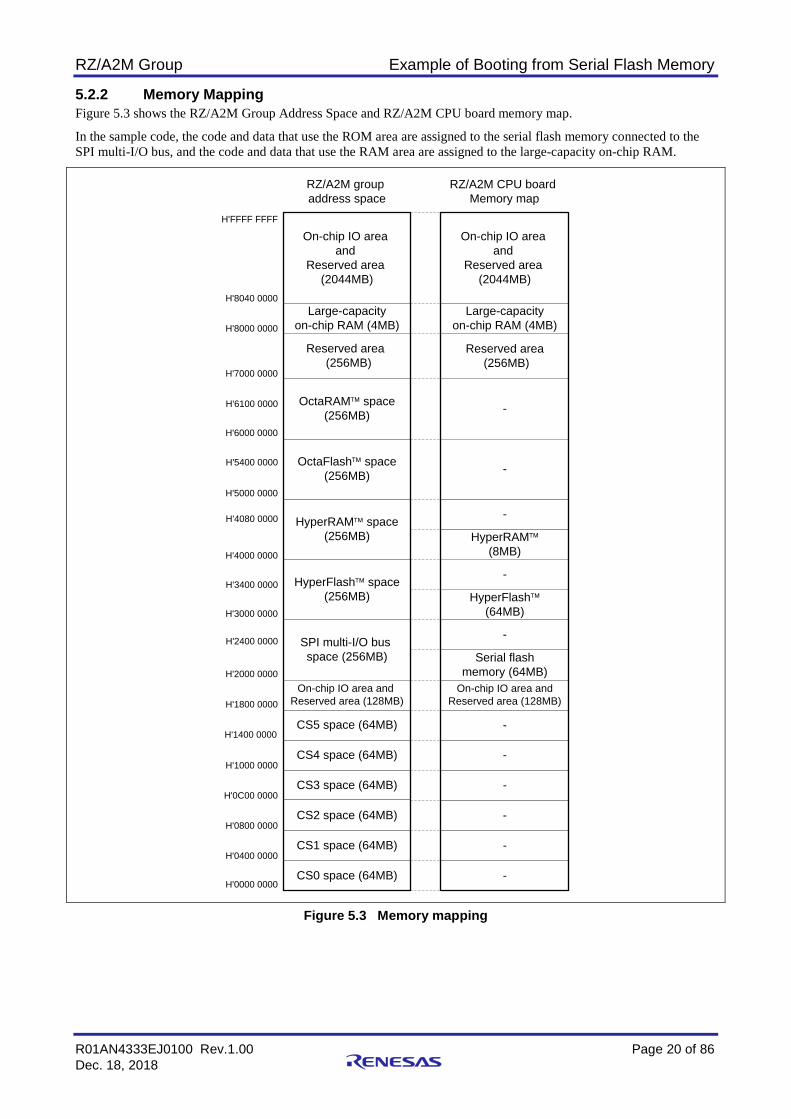
5.2.2 Memory Mapping Figure 5.3 shows the RZ/A2M Group Address Space and RZ/A2M CPU board memory map.
In the sample code, the code and data that use the ROM area are assigned to the serial flash memory connected to the SPI multi-I/O bus, and the code and data that use the RAM area are assigned to the large-capacity on-chip RAM.
Figure 5.3 Memory mapping
HyperFlash(64MB)
-
HyperRAM space (256MB)
HyperFlash space (256MB)
SPI multi-I/O busspace (256MB)
OctaFlash space (256MB)
H'FFFF FFFF
H'8040 0000
H'8000 0000
H'7000 0000
RZ/A2M groupaddress space
H'6000 0000
CS3 space (64MB)
CS2 space (64MB)
CS1 space (64MB)
CS4 space (64MB)
H'5000 0000
H'4000 0000
CS0 space (64MB)
H'2000 0000
H'1800 0000
On-chip IO areaand
Reserved area(2044MB)
H'1400 0000
H'1000 0000
OctaRAM space (256MB)
Reserved area (256MB)
Large-capacityon-chip RAM (4MB)
H'3000 0000
CS5 space (64MB)
On-chip IO area andReserved area (128MB)
H'0000 0000
H'0C00 0000
H'0800 0000
H'0400 0000
RZ/A2M CPU boardMemory map
-
-
-
-
-
On-chip IO areaand
Reserved area(2044MB)
Reserved area (256MB)
Large-capacityon-chip RAM (4MB)
-
On-chip IO area andReserved area (128MB)
-
-
H'2400 0000
H'3400 0000
H'4080 0000
H'5400 0000
H'6100 0000 -
-
HyperRAM(8MB)
Serial flashmemory (64MB)
RZ/A2M Group Example of Booting from Serial Flash Memory
R01AN4333EJ0100 Rev.1.00 Page 21 of 86 Dec. 18, 2018
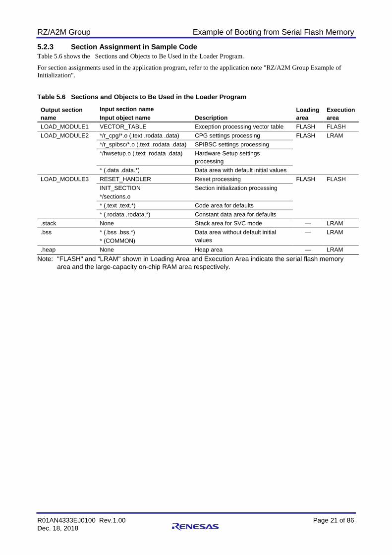
5.2.3 Section Assignment in Sample Code Table 5.6 shows the Sections and Objects to Be Used in the Loader Program.
For section assignments used in the application program, refer to the application note "RZ/A2M Group Example of Initialization".
Table 5.6 Sections and Objects to Be Used in the Loader Program
Output section name
Input section name Input object name Description
Loading area
Execution area
LOAD_MODULE1 VECTOR_TABLE Exception processing vector table FLASH FLASH LOAD_MODULE2 */r_cpg/*.o (.text .rodata .data) CPG settings processing FLASH LRAM
*/r_spibsc/*.o (.text .rodata .data) SPIBSC settings processing */hwsetup.o (.text .rodata .data) Hardware Setup settings
processing * (.data .data.*) Data area with default initial values
LOAD_MODULE3 RESET_HANDLER Reset processing FLASH FLASH INIT_SECTION */sections.o
Section initialization processing
* (.text .text.*) Code area for defaults * (.rodata .rodata.*) Constant data area for defaults
.stack None Stack area for SVC mode — LRAM
.bss * (.bss .bss.*) * (COMMON)
Data area without default initial values
— LRAM
.heap None Heap area — LRAM Note: "FLASH" and "LRAM" shown in Loading Area and Execution Area indicate the serial flash memory
area and the large-capacity on-chip RAM area respectively.

RZ/A2M Group Example of Booting from Serial Flash Memory
R01AN4333EJ0100 Rev.1.00 Page 22 of 86 Dec. 18, 2018
5.3 Interrupt Used Interrupt is not used in the loader program.
For interrupt used in the application program, refer to the application note "RZ/A2M Group Example of Initialization".
5.4 Data Types Table 5.7 shows the Data Types Used in the Sample Code.
Table 5.7 Data Types Used in the Sample Code
Symbol Description char_t 8-bit character bool_t Boolean type. Value is true (1) or false (0). int_t Fast integer, signed, 32-bit integer in this sample code int8_t 8-bit integer, signed (defined in standard library stdint.h) int16_t 16-bit integer, signed (defined in standard library stdint.h) int32_t 32-bit integer, signed (defined in standard library stdint.h) int64_t 64-bit integer, signed (defined in standard library stdint.h) uint8_t 8-bit integer, unsigned (defined in standard library stdint.h) uint16_t 16-bit integer, unsigned (defined in standard library stdint.h) uint32_t 32-bit integer, unsigned (defined in standard library stdint.h) uint64_t 64-bit integer, unsigned (defined in standard library stdint.h) float32_t 32-bit float float64_t 64-bit float float128_t 128-bit float
RZ/A2M Group Example of Booting from Serial Flash Memory
R01AN4333EJ0100 Rev.1.00 Page 23 of 86 Dec. 18, 2018
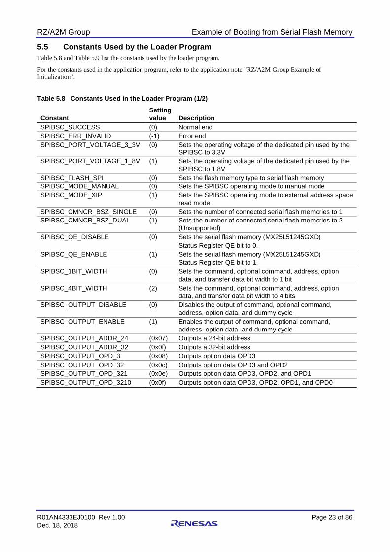
5.5 Constants Used by the Loader Program Table 5.8 and Table 5.9 list the constants used by the loader program.
For the constants used in the application program, refer to the application note "RZ/A2M Group Example of Initialization".
Table 5.8 Constants Used in the Loader Program (1/2)
Constant Setting value Description
SPIBSC_SUCCESS (0) Normal end SPIBSC_ERR_INVALID (-1) Error end SPIBSC_PORT_VOLTAGE_3_3V (0) Sets the operating voltage of the dedicated pin used by the
SPIBSC to 3.3V SPIBSC_PORT_VOLTAGE_1_8V (1) Sets the operating voltage of the dedicated pin used by the
SPIBSC to 1.8V SPIBSC_FLASH_SPI (0) Sets the flash memory type to serial flash memory SPIBSC_MODE_MANUAL (0) Sets the SPIBSC operating mode to manual mode SPIBSC_MODE_XIP (1) Sets the SPIBSC operating mode to external address space
read mode SPIBSC_CMNCR_BSZ_SINGLE (0) Sets the number of connected serial flash memories to 1 SPIBSC_CMNCR_BSZ_DUAL (1) Sets the number of connected serial flash memories to 2
(Unsupported) SPIBSC_QE_DISABLE (0) Sets the serial flash memory (MX25L51245GXD)
Status Register QE bit to 0. SPIBSC_QE_ENABLE (1) Sets the serial flash memory (MX25L51245GXD)
Status Register QE bit to 1. SPIBSC_1BIT_WIDTH (0) Sets the command, optional command, address, option
data, and transfer data bit width to 1 bit SPIBSC_4BIT_WIDTH (2) Sets the command, optional command, address, option
data, and transfer data bit width to 4 bits SPIBSC_OUTPUT_DISABLE (0) Disables the output of command, optional command,
address, option data, and dummy cycle SPIBSC_OUTPUT_ENABLE (1) Enables the output of command, optional command,
address, option data, and dummy cycle SPIBSC_OUTPUT_ADDR_24 (0x07) Outputs a 24-bit address SPIBSC_OUTPUT_ADDR_32 (0x0f) Outputs a 32-bit address SPIBSC_OUTPUT_OPD_3 (0x08) Outputs option data OPD3 SPIBSC_OUTPUT_OPD_32 (0x0c) Outputs option data OPD3 and OPD2 SPIBSC_OUTPUT_OPD_321 (0x0e) Outputs option data OPD3, OPD2, and OPD1 SPIBSC_OUTPUT_OPD_3210 (0x0f) Outputs option data OPD3, OPD2, OPD1, and OPD0
RZ/A2M Group Example of Booting from Serial Flash Memory
R01AN4333EJ0100 Rev.1.00 Page 24 of 86 Dec. 18, 2018
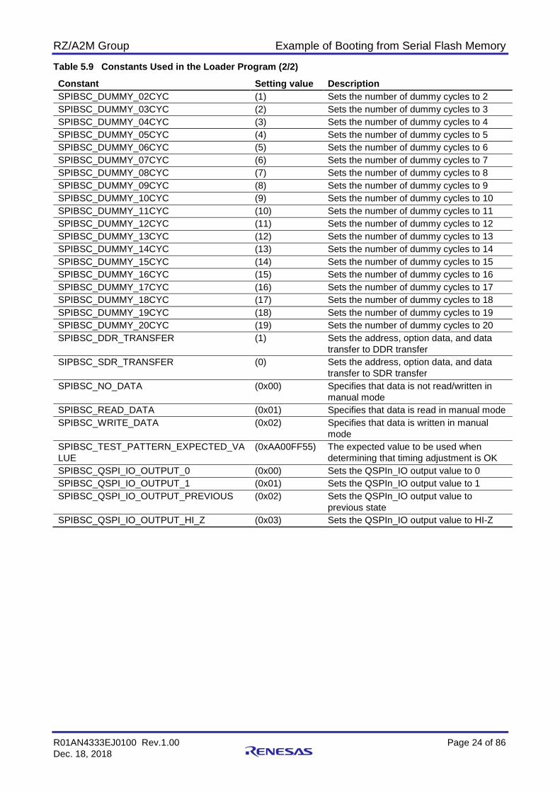
Table 5.9 Constants Used in the Loader Program (2/2)
Constant Setting value Description SPIBSC_DUMMY_02CYC (1) Sets the number of dummy cycles to 2 SPIBSC_DUMMY_03CYC (2) Sets the number of dummy cycles to 3 SPIBSC_DUMMY_04CYC (3) Sets the number of dummy cycles to 4 SPIBSC_DUMMY_05CYC (4) Sets the number of dummy cycles to 5 SPIBSC_DUMMY_06CYC (5) Sets the number of dummy cycles to 6 SPIBSC_DUMMY_07CYC (6) Sets the number of dummy cycles to 7 SPIBSC_DUMMY_08CYC (7) Sets the number of dummy cycles to 8 SPIBSC_DUMMY_09CYC (8) Sets the number of dummy cycles to 9 SPIBSC_DUMMY_10CYC (9) Sets the number of dummy cycles to 10 SPIBSC_DUMMY_11CYC (10) Sets the number of dummy cycles to 11 SPIBSC_DUMMY_12CYC (11) Sets the number of dummy cycles to 12 SPIBSC_DUMMY_13CYC (12) Sets the number of dummy cycles to 13 SPIBSC_DUMMY_14CYC (13) Sets the number of dummy cycles to 14 SPIBSC_DUMMY_15CYC (14) Sets the number of dummy cycles to 15 SPIBSC_DUMMY_16CYC (15) Sets the number of dummy cycles to 16 SPIBSC_DUMMY_17CYC (16) Sets the number of dummy cycles to 17 SPIBSC_DUMMY_18CYC (17) Sets the number of dummy cycles to 18 SPIBSC_DUMMY_19CYC (18) Sets the number of dummy cycles to 19 SPIBSC_DUMMY_20CYC (19) Sets the number of dummy cycles to 20 SPIBSC_DDR_TRANSFER (1) Sets the address, option data, and data
transfer to DDR transfer SIPBSC_SDR_TRANSFER (0) Sets the address, option data, and data
transfer to SDR transfer SPIBSC_NO_DATA (0x00) Specifies that data is not read/written in
manual mode SPIBSC_READ_DATA (0x01) Specifies that data is read in manual mode SPIBSC_WRITE_DATA (0x02) Specifies that data is written in manual
mode SPIBSC_TEST_PATTERN_EXPECTED_VALUE
(0xAA00FF55) The expected value to be used when determining that timing adjustment is OK
SPIBSC_QSPI_IO_OUTPUT_0 (0x00) Sets the QSPIn_IO output value to 0 SPIBSC_QSPI_IO_OUTPUT_1 (0x01) Sets the QSPIn_IO output value to 1 SPIBSC_QSPI_IO_OUTPUT_PREVIOUS (0x02) Sets the QSPIn_IO output value to
previous state SPIBSC_QSPI_IO_OUTPUT_HI_Z (0x03) Sets the QSPIn_IO output value to HI-Z
RZ/A2M Group Example of Booting from Serial Flash Memory
R01AN4333EJ0100 Rev.1.00 Page 25 of 86 Dec. 18, 2018
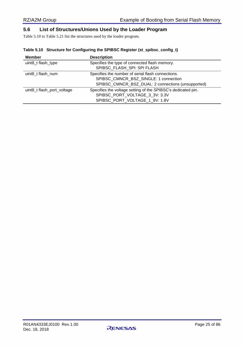
5.6 List of Structures/Unions Used by the Loader Program Table 5.10 to Table 5.21 list the structures used by the loader program.
Table 5.10 Structure for Configuring the SPIBSC Register (st_spibsc_config_t)
Member Description uint8_t flash_type Specifies the type of connected flash memory.
SPIBSC_FLASH_SPI: SPI FLASH uint8_t flash_num Specifies the number of serial flash connections.
SPIBSC_CMNCR_BSZ_SINGLE: 1 connection SPIBSC_CMNCR_BSZ_DUAL: 2 connections (unsupported)
uint8_t flash_port_voltage Specifies the voltage setting of the SPIBSC's dedicated pin. SPIBSC_PORT_VOLTAGE_3_3V: 3.3V SPIBSC_PORT_VOLTAGE_1_8V: 1.8V
RZ/A2M Group Example of Booting from Serial Flash Memory
R01AN4333EJ0100 Rev.1.00 Page 26 of 86 Dec. 18, 2018
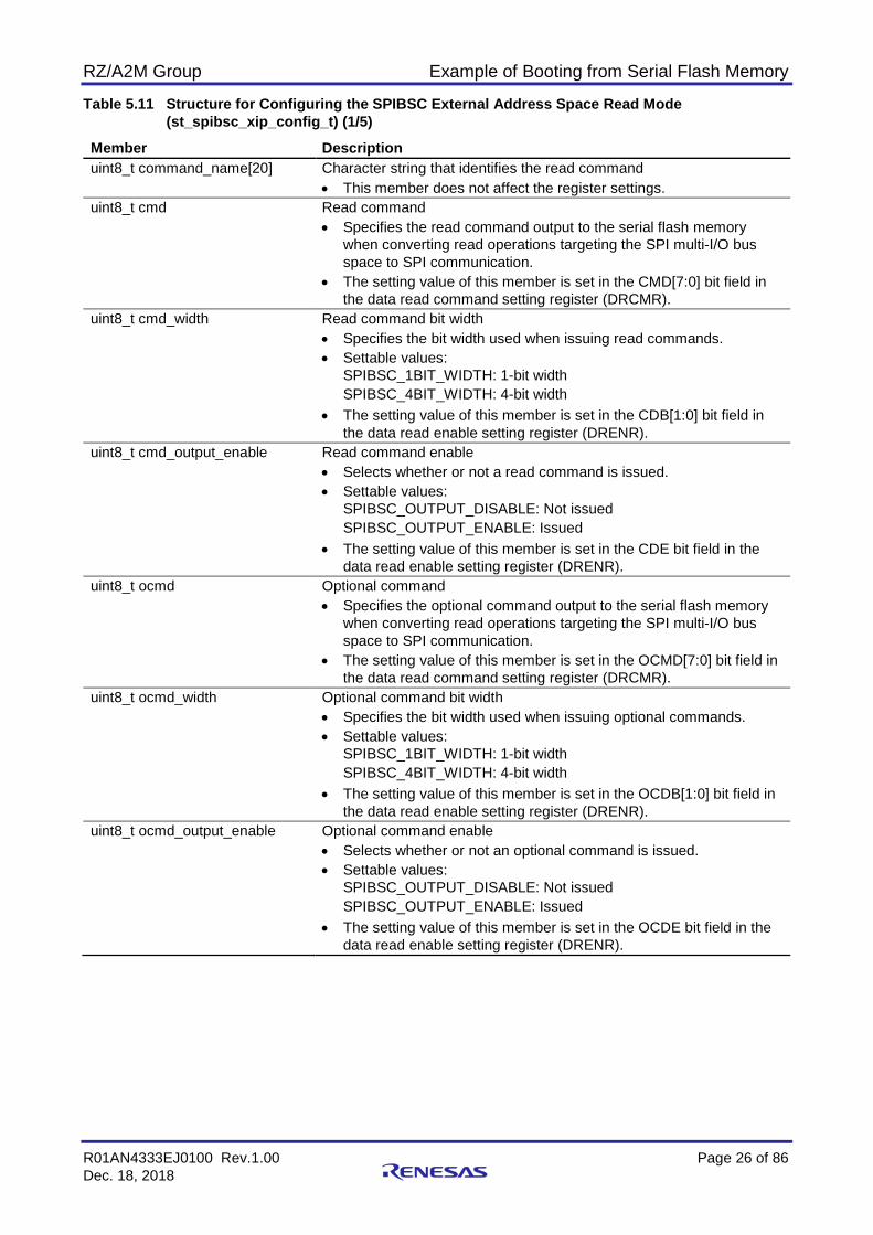
Table 5.11 Structure for Configuring the SPIBSC External Address Space Read Mode (st_spibsc_xip_config_t) (1/5)
Member Description uint8_t command_name[20] Character string that identifies the read command
• This member does not affect the register settings. uint8_t cmd Read command
• Specifies the read command output to the serial flash memory when converting read operations targeting the SPI multi-I/O bus space to SPI communication.
• The setting value of this member is set in the CMD[7:0] bit field in the data read command setting register (DRCMR).
uint8_t cmd_width Read command bit width • Specifies the bit width used when issuing read commands. • Settable values:
SPIBSC_1BIT_WIDTH: 1-bit width SPIBSC_4BIT_WIDTH: 4-bit width
• The setting value of this member is set in the CDB[1:0] bit field in the data read enable setting register (DRENR).
uint8_t cmd_output_enable Read command enable • Selects whether or not a read command is issued. • Settable values:
SPIBSC_OUTPUT_DISABLE: Not issued SPIBSC_OUTPUT_ENABLE: Issued
• The setting value of this member is set in the CDE bit field in the data read enable setting register (DRENR).
uint8_t ocmd Optional command • Specifies the optional command output to the serial flash memory
when converting read operations targeting the SPI multi-I/O bus space to SPI communication.
• The setting value of this member is set in the OCMD[7:0] bit field in the data read command setting register (DRCMR).
uint8_t ocmd_width Optional command bit width • Specifies the bit width used when issuing optional commands. • Settable values:
SPIBSC_1BIT_WIDTH: 1-bit width SPIBSC_4BIT_WIDTH: 4-bit width
• The setting value of this member is set in the OCDB[1:0] bit field in the data read enable setting register (DRENR).
uint8_t ocmd_output_enable Optional command enable • Selects whether or not an optional command is issued. • Settable values:
SPIBSC_OUTPUT_DISABLE: Not issued SPIBSC_OUTPUT_ENABLE: Issued
• The setting value of this member is set in the OCDE bit field in the data read enable setting register (DRENR).
RZ/A2M Group Example of Booting from Serial Flash Memory
R01AN4333EJ0100 Rev.1.00 Page 27 of 86 Dec. 18, 2018
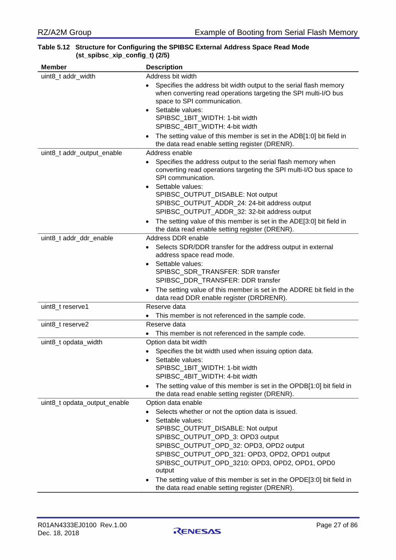
Table 5.12 Structure for Configuring the SPIBSC External Address Space Read Mode (st_spibsc_xip_config_t) (2/5)
Member Description uint8_t addr_width Address bit width
• Specifies the address bit width output to the serial flash memory when converting read operations targeting the SPI multi-I/O bus space to SPI communication.
• Settable values: SPIBSC_1BIT_WIDTH: 1-bit width SPIBSC_4BIT_WIDTH: 4-bit width
• The setting value of this member is set in the ADB[1:0] bit field in the data read enable setting register (DRENR).
uint8_t addr_output_enable Address enable • Specifies the address output to the serial flash memory when
converting read operations targeting the SPI multi-I/O bus space to SPI communication.
• Settable values: SPIBSC_OUTPUT_DISABLE: Not output SPIBSC_OUTPUT_ADDR_24: 24-bit address output SPIBSC_OUTPUT_ADDR_32: 32-bit address output
• The setting value of this member is set in the ADE[3:0] bit field in the data read enable setting register (DRENR).
uint8_t addr_ddr_enable Address DDR enable • Selects SDR/DDR transfer for the address output in external
address space read mode. • Settable values:
SPIBSC_SDR_TRANSFER: SDR transfer SPIBSC_DDR_TRANSFER: DDR transfer
• The setting value of this member is set in the ADDRE bit field in the data read DDR enable register (DRDRENR).
uint8_t reserve1 Reserve data • This member is not referenced in the sample code.
uint8_t reserve2 Reserve data • This member is not referenced in the sample code.
uint8_t opdata_width Option data bit width • Specifies the bit width used when issuing option data. • Settable values:
SPIBSC_1BIT_WIDTH: 1-bit width SPIBSC_4BIT_WIDTH: 4-bit width
• The setting value of this member is set in the OPDB[1:0] bit field in the data read enable setting register (DRENR).
uint8_t opdata_output_enable Option data enable • Selects whether or not the option data is issued. • Settable values:
SPIBSC_OUTPUT_DISABLE: Not output SPIBSC_OUTPUT_OPD_3: OPD3 output SPIBSC_OUTPUT_OPD_32: OPD3, OPD2 output SPIBSC_OUTPUT_OPD_321: OPD3, OPD2, OPD1 output SPIBSC_OUTPUT_OPD_3210: OPD3, OPD2, OPD1, OPD0 output
• The setting value of this member is set in the OPDE[3:0] bit field in the data read enable setting register (DRENR).

RZ/A2M Group Example of Booting from Serial Flash Memory
R01AN4333EJ0100 Rev.1.00 Page 28 of 86 Dec. 18, 2018
Table 5.13 Structure for Configuring the SPIBSC External Address Space Read Mode (st_spibsc_xip_config_t) (3/5)
Member Description uint8_t opdata_ddr_enable Option data DDR enable
• Selects SDR/DDR transfer for the option data output in external address space read mode.
• Settable values: SPIBSC_SDR_TRANSFER: SDR transfer SPIBSC_DDR_TRANSFER: DDR transfer
• The setting value of this member is set in the OPDRE bit field in the data read DDR enable register (DRDRENR).
uint8_t opd3 uint8_t opd2 uint8_t opd1 uint8_t opd0
Option data • Specifies the option data output to the serial flash memory when
converting read operations targeting the SPI multi-I/O bus space to SPI communication.
• The setting value of this member is set in the OPD3[7:0], OPD2[7:0], OPD1[7:0], and OPD0[7:0] bit fields in the data read option setting register (DROPR).
uint8_t reserve3 Reserve data This member is not referenced in the sample code.
uint8_t dummy_cycle_enable Dummy cycle enable • Selects whether or not dummy cycles are inserted. • Settable values:
SPIBSC_OUTPUT_DISABLE: Not inserted SPIBSC_OUTPUT_ENABLE: Inserted
• The setting value of this member is set in the DME bit field in the data read enable setting register (DRENR).
uint8_t dummy_cycle_count Number of dummy cycles • Sets the number of inserted dummy cycles. • Settable values:
SPIBSC_DUMMY_02CYC to SPIBSC_DUMMY_20CYC • The setting value of this member is set in the DMCYC[4:0] bit field
in the data read dummy cycle setting register (DRDMCR). uint8_t data_width Data read bit width
• Specifies the data read bit width of the serial flash memory when converting read operations targeting the SPI multi-I/O bus space to SPI communication.
• Settable values: SPIBSC_1BIT_WIDTH: 1-bit width SPIBSC_4BIT_WIDTH: 4-bit width
• The setting value of this member is set in the DRDB[1:0] bit field in the data read enable setting register (DRENR).
uint8_t data_ddr_enable Transfer data DDR enable • Selects SDR/DDR transfer for the data transferred in external
address space read mode. • Settable values:
SPIBSC_SDR_TRANSFER: SDR transfer SPIBSC_DDR_TRANSFER: DDR transfer
• The setting value of this member is set in the DRDRE bit field in the data read DDR enable register (DRDRENR).

RZ/A2M Group Example of Booting from Serial Flash Memory
R01AN4333EJ0100 Rev.1.00 Page 29 of 86 Dec. 18, 2018
Table 5.14 Structure for Configuring the SPIBSC External Address Space Read Mode (st_spibsc_xip_config_t) (4/5)
Member Description uint8_t cmncr_moiio3 Level for QSPIn_IO3 while SSL negated.
• Specify the level after finished the data transfer. • Settable values:
SPIBSC_QSPI_IO_OUTPUT_0: The output value is 0. SPIBSC_QSPI_IO_OUTPUT_1: The output value is 1. SPIBSC_QSPI_IO_OUTPUT_PREVIOUS: The output value is that of the last bit in the previous transfer (the pin is placed in the Hi-Z state if that was the case in the previous transfer). SPIBSC_QSPI_IO_OUTPUT_HI_Z: The pin is placed in the Hi-Z state.
The setting value of this member is set in the MOIIO3[1:0] bit field in the Common Control Register (CMNCR).
uint8_t cmncr_moiio2 Level for QSPIn_IO2 while SSL negated. • Specify the level after finished the data transfer. • Settable values:
SPIBSC_QSPI_IO_OUTPUT_0: The output value is 0. SPIBSC_QSPI_IO_OUTPUT_1: The output value is 1. SPIBSC_QSPI_IO_OUTPUT_PREVIOUS: The output value is that of the last bit in the previous transfer (the pin is placed in the Hi-Z state if that was the case in the previous transfer). SPIBSC_QSPI_IO_OUTPUT_HI_Z: The pin is placed in the Hi-Z state.
The setting value of this member is set in the MOIIO2[1:0] bit field in the Common Control Register (CMNCR).
uint8_t cmncr_moiio1 Level for QSPIn_IO1 while SSL negated. • Specify the level after finished the data transfer. • Settable values:
SPIBSC_QSPI_IO_OUTPUT_0: The output value is 0. SPIBSC_QSPI_IO_OUTPUT_1: The output value is 1. SPIBSC_QSPI_IO_OUTPUT_PREVIOUS: The output value is that of the last bit in the previous transfer (the pin is placed in the Hi-Z state if that was the case in the previous transfer). SPIBSC_QSPI_IO_OUTPUT_HI_Z: The pin is placed in the Hi-Z state.
The setting value of this member is set in the MOIIO1[1:0] bit field in the Common Control Register (CMNCR).
uint8_t cmncr_moiio0 Level for QSPIn_IO0 while SSL negated. • Specify the level after finished the data transfer. • Settable values:
SPIBSC_QSPI_IO_OUTPUT_0: The output value is 0. SPIBSC_QSPI_IO_OUTPUT_1: The output value is 1. SPIBSC_QSPI_IO_OUTPUT_PREVIOUS: The output value is that of the last bit in the previous transfer (the pin is placed in the Hi-Z state if that was the case in the previous transfer). SPIBSC_QSPI_IO_OUTPUT_HI_Z: The pin is placed in the Hi-Z state.
The setting value of this member is set in the MOIIO0[1:0] bit field in the Common Control Register (CMNCR).

RZ/A2M Group Example of Booting from Serial Flash Memory
R01AN4333EJ0100 Rev.1.00 Page 30 of 86 Dec. 18, 2018
Table 5.15 Structure for Configuring the SPIBSC External Address Space Read Mode (st_spibsc_xip_config_t) (5/5)
Member Description uint8_t cmncr_io3fv Level for QSPIn_IO3 while 1-bit width transfer.
• Specify the level while the data transfer is by 1-bit width. • Settable values:
SPIBSC_QSPI_IO_OUTPUT_0: The output value is 0. SPIBSC_QSPI_IO_OUTPUT_1: The output value is 1. SPIBSC_QSPI_IO_OUTPUT_PREVIOUS: The output value is that of the last bit in the previous transfer (the pin is placed in the Hi-Z state if that was the case in the previous transfer). SPIBSC_QSPI_IO_OUTPUT_HI_Z: The pin is placed in the Hi-Z state.
The setting value of this member is set in the IO3FV[1:0] bit field in the Common Control Register (CMNCR).
uint8_t cmncr_io2fv Level for QSPIn_IO2 while 1-bit width transfer. • Specify the level while the data transfer is by 1-bit width. • Settable values:
SPIBSC_QSPI_IO_OUTPUT_0: The output value is 0. SPIBSC_QSPI_IO_OUTPUT_1: The output value is 1. SPIBSC_QSPI_IO_OUTPUT_PREVIOUS: The output value is that of the last bit in the previous transfer (the pin is placed in the Hi-Z state if that was the case in the previous transfer). SPIBSC_QSPI_IO_OUTPUT_HI_Z: The pin is placed in the Hi-Z state.
The setting value of this member is set in the IO2FV[1:0] bit field in the Common Control Register (CMNCR).
uint8_t cmncr_io0fv Level for QSPIn_IO0 while 1-bit width read transfer. • Specify the level while the data read transfer is by 1-bit width. • Settable values:
SPIBSC_QSPI_IO_OUTPUT_0: The output value is 0. SPIBSC_QSPI_IO_OUTPUT_1: The output value is 1. SPIBSC_QSPI_IO_OUTPUT_PREVIOUS: The output value is that of the last bit in the previous transfer (the pin is placed in the Hi-Z state if that was the case in the previous transfer). SPIBSC_QSPI_IO_OUTPUT_HI_Z: The pin is placed in the Hi-Z state.
The setting value of this member is set in the IO3FV[1:0] bit field in the Common Control Register (CMNCR).
RZ/A2M Group Example of Booting from Serial Flash Memory
R01AN4333EJ0100 Rev.1.00 Page 31 of 86 Dec. 18, 2018
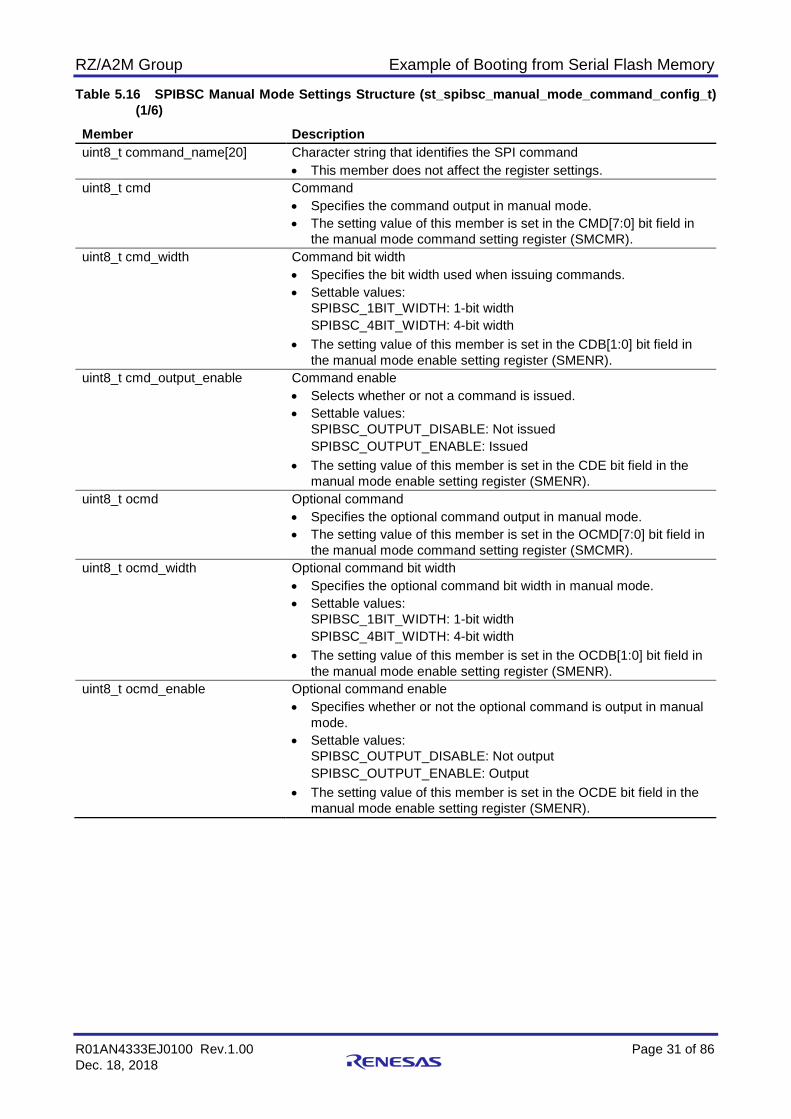
Table 5.16 SPIBSC Manual Mode Settings Structure (st_spibsc_manual_mode_command_config_t) (1/6)
Member Description uint8_t command_name[20] Character string that identifies the SPI command
• This member does not affect the register settings. uint8_t cmd Command
• Specifies the command output in manual mode. • The setting value of this member is set in the CMD[7:0] bit field in
the manual mode command setting register (SMCMR). uint8_t cmd_width Command bit width
• Specifies the bit width used when issuing commands. • Settable values:
SPIBSC_1BIT_WIDTH: 1-bit width SPIBSC_4BIT_WIDTH: 4-bit width
• The setting value of this member is set in the CDB[1:0] bit field in the manual mode enable setting register (SMENR).
uint8_t cmd_output_enable Command enable • Selects whether or not a command is issued. • Settable values:
SPIBSC_OUTPUT_DISABLE: Not issued SPIBSC_OUTPUT_ENABLE: Issued
• The setting value of this member is set in the CDE bit field in the manual mode enable setting register (SMENR).
uint8_t ocmd Optional command • Specifies the optional command output in manual mode. • The setting value of this member is set in the OCMD[7:0] bit field in
the manual mode command setting register (SMCMR). uint8_t ocmd_width Optional command bit width
• Specifies the optional command bit width in manual mode. • Settable values:
SPIBSC_1BIT_WIDTH: 1-bit width SPIBSC_4BIT_WIDTH: 4-bit width
• The setting value of this member is set in the OCDB[1:0] bit field in the manual mode enable setting register (SMENR).
uint8_t ocmd_enable Optional command enable • Specifies whether or not the optional command is output in manual
mode. • Settable values:
SPIBSC_OUTPUT_DISABLE: Not output SPIBSC_OUTPUT_ENABLE: Output
• The setting value of this member is set in the OCDE bit field in the manual mode enable setting register (SMENR).
RZ/A2M Group Example of Booting from Serial Flash Memory
R01AN4333EJ0100 Rev.1.00 Page 32 of 86 Dec. 18, 2018
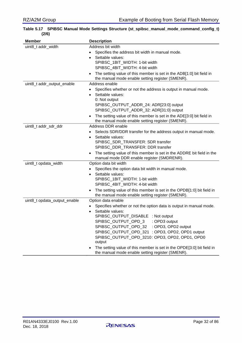
Table 5.17 SPIBSC Manual Mode Settings Structure (st_spibsc_manual_mode_command_config_t) (2/6)
Member Description uint8_t addr_width Address bit width
• Specifies the address bit width in manual mode. • Settable values:
SPIBSC_1BIT_WIDTH: 1-bit width SPIBSC_4BIT_WIDTH: 4-bit width
• The setting value of this member is set in the ADB[1:0] bit field in the manual mode enable setting register (SMENR).
uint8_t addr_output_enable Address enable • Specifies whether or not the address is output in manual mode. • Settable values:
0: Not output SPIBSC_OUTPUT_ADDR_24: ADR[23:0] output SPIBSC_OUTPUT_ADDR_32: ADR[31:0] output
• The setting value of this member is set in the ADE[3:0] bit field in the manual mode enable setting register (SMENR).
uint8_t addr_sdr_ddr Address DDR enable • Selects SDR/DDR transfer for the address output in manual mode. • Settable values:
SPIBSC_SDR_TRANSFER: SDR transfer SPIBSC_DDR_TRANSFER: DDR transfer
• The setting value of this member is set in the ADDRE bit field in the manual mode DDR enable register (SMDRENR).
uint8_t opdata_width Option data bit width • Specifies the option data bit width in manual mode. • Settable values:
SPIBSC_1BIT_WIDTH: 1-bit width SPIBSC_4BIT_WIDTH: 4-bit width
• The setting value of this member is set in the OPDB[1:0] bit field in the manual mode enable setting register (SMENR).
uint8_t opdata_output_enable Option data enable • Specifies whether or not the option data is output in manual mode. • Settable values:
SPIBSC_OUTPUT_DISABLE : Not output SPIBSC_OUTPUT_OPD_3 : OPD3 output SPIBSC_OUTPUT_OPD_32 : OPD3, OPD2 output SPIBSC_OUTPUT_OPD_321 : OPD3, OPD2, OPD1 output SPIBSC_OUTPUT_OPD_3210 : OPD3, OPD2, OPD1, OPD0 output
• The setting value of this member is set in the OPDE[3:0] bit field in the manual mode enable setting register (SMENR).
RZ/A2M Group Example of Booting from Serial Flash Memory
R01AN4333EJ0100 Rev.1.00 Page 33 of 86 Dec. 18, 2018
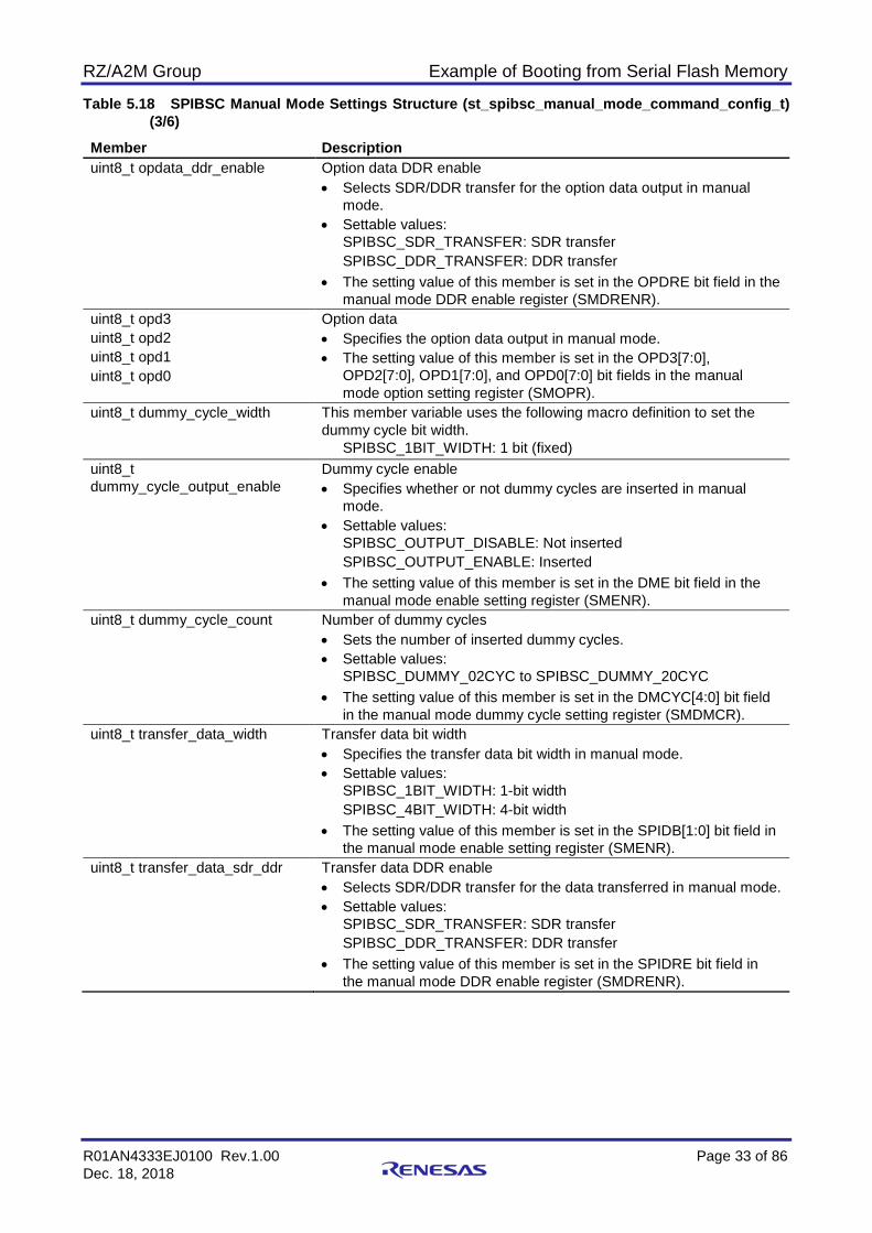
Table 5.18 SPIBSC Manual Mode Settings Structure (st_spibsc_manual_mode_command_config_t) (3/6)
Member Description uint8_t opdata_ddr_enable Option data DDR enable
• Selects SDR/DDR transfer for the option data output in manual mode.
• Settable values: SPIBSC_SDR_TRANSFER: SDR transfer SPIBSC_DDR_TRANSFER: DDR transfer
• The setting value of this member is set in the OPDRE bit field in the manual mode DDR enable register (SMDRENR).
uint8_t opd3 uint8_t opd2 uint8_t opd1 uint8_t opd0
Option data • Specifies the option data output in manual mode. • The setting value of this member is set in the OPD3[7:0],
OPD2[7:0], OPD1[7:0], and OPD0[7:0] bit fields in the manual mode option setting register (SMOPR).
uint8_t dummy_cycle_width This member variable uses the following macro definition to set the dummy cycle bit width.
SPIBSC_1BIT_WIDTH: 1 bit (fixed) uint8_t dummy_cycle_output_enable
Dummy cycle enable • Specifies whether or not dummy cycles are inserted in manual
mode. • Settable values:
SPIBSC_OUTPUT_DISABLE: Not inserted SPIBSC_OUTPUT_ENABLE: Inserted
• The setting value of this member is set in the DME bit field in the manual mode enable setting register (SMENR).
uint8_t dummy_cycle_count Number of dummy cycles • Sets the number of inserted dummy cycles. • Settable values:
SPIBSC_DUMMY_02CYC to SPIBSC_DUMMY_20CYC • The setting value of this member is set in the DMCYC[4:0] bit field
in the manual mode dummy cycle setting register (SMDMCR). uint8_t transfer_data_width Transfer data bit width
• Specifies the transfer data bit width in manual mode. • Settable values:
SPIBSC_1BIT_WIDTH: 1-bit width SPIBSC_4BIT_WIDTH: 4-bit width
• The setting value of this member is set in the SPIDB[1:0] bit field in the manual mode enable setting register (SMENR).
uint8_t transfer_data_sdr_ddr Transfer data DDR enable • Selects SDR/DDR transfer for the data transferred in manual mode. • Settable values:
SPIBSC_SDR_TRANSFER: SDR transfer SPIBSC_DDR_TRANSFER: DDR transfer
• The setting value of this member is set in the SPIDRE bit field in the manual mode DDR enable register (SMDRENR).

RZ/A2M Group Example of Booting from Serial Flash Memory
R01AN4333EJ0100 Rev.1.00 Page 34 of 86 Dec. 18, 2018
Table 5.19 SPIBSC Manual Mode Settings Structure (st_spibsc_manual_mode_command_config_t) (4/6)
Member Description uint8_t reserve1 Reserve data
• This member is not referenced in the sample code. uint8_t reserve2 Reserve data
• This member is not referenced in the sample code. uint8_t cmncr_moiio3 Level for QSPIn_IO3 while SSL negated.
• Specify the level after finished the data transfer. • Settable values:
SPIBSC_QSPI_IO_OUTPUT_0: The output value is 0. SPIBSC_QSPI_IO_OUTPUT_1: The output value is 1. SPIBSC_QSPI_IO_OUTPUT_PREVIOUS: The output value is that of the last bit in the previous transfer (the pin is placed in the Hi-Z state if that was the case in the previous transfer). SPIBSC_QSPI_IO_OUTPUT_HI_Z: The pin is placed in the Hi-Z state.
• The setting value of this member is set in the MOIIO3[1:0] bit field in the Common Control Register (CMNCR).
uint8_t cmncr_moiio2 Level for QSPIn_IO2 while SSL negated. • Specify the level after finished the data transfer. • Settable values:
SPIBSC_QSPI_IO_OUTPUT_0: The output value is 0. SPIBSC_QSPI_IO_OUTPUT_1: The output value is 1. SPIBSC_QSPI_IO_OUTPUT_PREVIOUS: The output value is that of the last bit in the previous transfer (the pin is placed in the Hi-Z state if that was the case in the previous transfer). SPIBSC_QSPI_IO_OUTPUT_HI_Z: The pin is placed in the Hi-Z state.
• The setting value of this member is set in the MOIIO2[1:0] bit field in the Common Control Register (CMNCR).
uint8_t cmncr_moiio1 Level for QSPIn_IO1 while SSL negated. • Specify the level after finished the data transfer. • Settable values:
SPIBSC_QSPI_IO_OUTPUT_0: The output value is 0. SPIBSC_QSPI_IO_OUTPUT_1: The output value is 1. SPIBSC_QSPI_IO_OUTPUT_PREVIOUS: The output value is that of the last bit in the previous transfer (the pin is placed in the Hi-Z state if that was the case in the previous transfer). SPIBSC_QSPI_IO_OUTPUT_HI_Z: The pin is placed in the Hi-Z state.
• The setting value of this member is set in the MOIIO1[1:0] bit field in the Common Control Register (CMNCR).
RZ/A2M Group Example of Booting from Serial Flash Memory
R01AN4333EJ0100 Rev.1.00 Page 35 of 86 Dec. 18, 2018
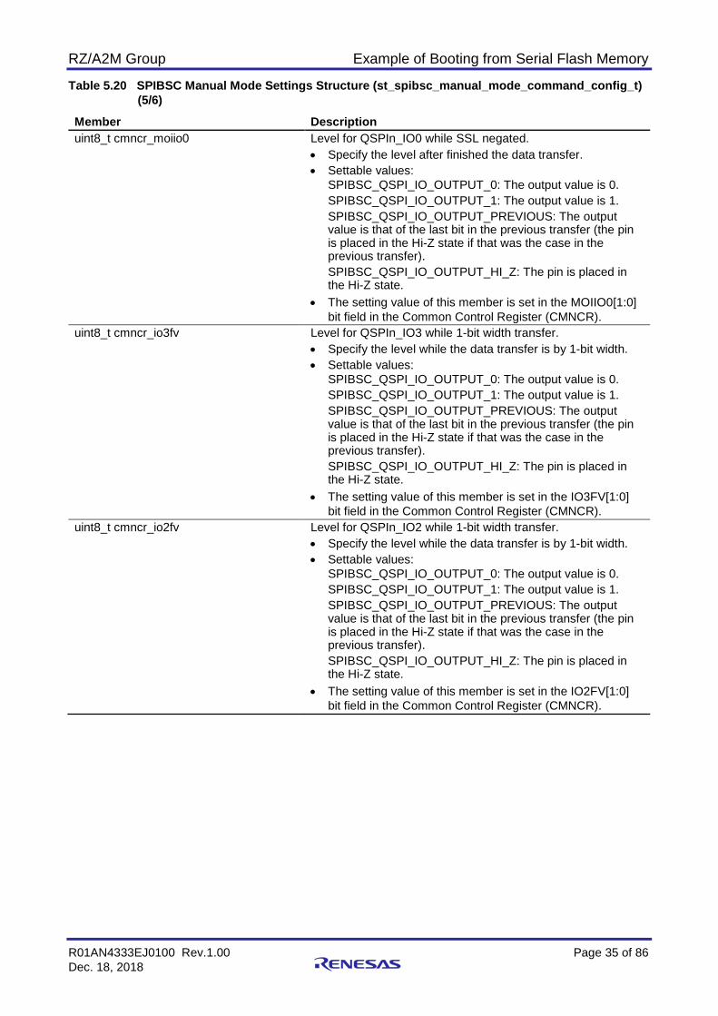
Table 5.20 SPIBSC Manual Mode Settings Structure (st_spibsc_manual_mode_command_config_t) (5/6)
Member Description uint8_t cmncr_moiio0 Level for QSPIn_IO0 while SSL negated.
• Specify the level after finished the data transfer. • Settable values:
SPIBSC_QSPI_IO_OUTPUT_0: The output value is 0. SPIBSC_QSPI_IO_OUTPUT_1: The output value is 1. SPIBSC_QSPI_IO_OUTPUT_PREVIOUS: The output value is that of the last bit in the previous transfer (the pin is placed in the Hi-Z state if that was the case in the previous transfer). SPIBSC_QSPI_IO_OUTPUT_HI_Z: The pin is placed in the Hi-Z state.
• The setting value of this member is set in the MOIIO0[1:0] bit field in the Common Control Register (CMNCR).
uint8_t cmncr_io3fv Level for QSPIn_IO3 while 1-bit width transfer. • Specify the level while the data transfer is by 1-bit width. • Settable values:
SPIBSC_QSPI_IO_OUTPUT_0: The output value is 0. SPIBSC_QSPI_IO_OUTPUT_1: The output value is 1. SPIBSC_QSPI_IO_OUTPUT_PREVIOUS: The output value is that of the last bit in the previous transfer (the pin is placed in the Hi-Z state if that was the case in the previous transfer). SPIBSC_QSPI_IO_OUTPUT_HI_Z: The pin is placed in the Hi-Z state.
• The setting value of this member is set in the IO3FV[1:0] bit field in the Common Control Register (CMNCR).
uint8_t cmncr_io2fv Level for QSPIn_IO2 while 1-bit width transfer. • Specify the level while the data transfer is by 1-bit width. • Settable values:
SPIBSC_QSPI_IO_OUTPUT_0: The output value is 0. SPIBSC_QSPI_IO_OUTPUT_1: The output value is 1. SPIBSC_QSPI_IO_OUTPUT_PREVIOUS: The output value is that of the last bit in the previous transfer (the pin is placed in the Hi-Z state if that was the case in the previous transfer). SPIBSC_QSPI_IO_OUTPUT_HI_Z: The pin is placed in the Hi-Z state.
• The setting value of this member is set in the IO2FV[1:0] bit field in the Common Control Register (CMNCR).
RZ/A2M Group Example of Booting from Serial Flash Memory
R01AN4333EJ0100 Rev.1.00 Page 36 of 86 Dec. 18, 2018
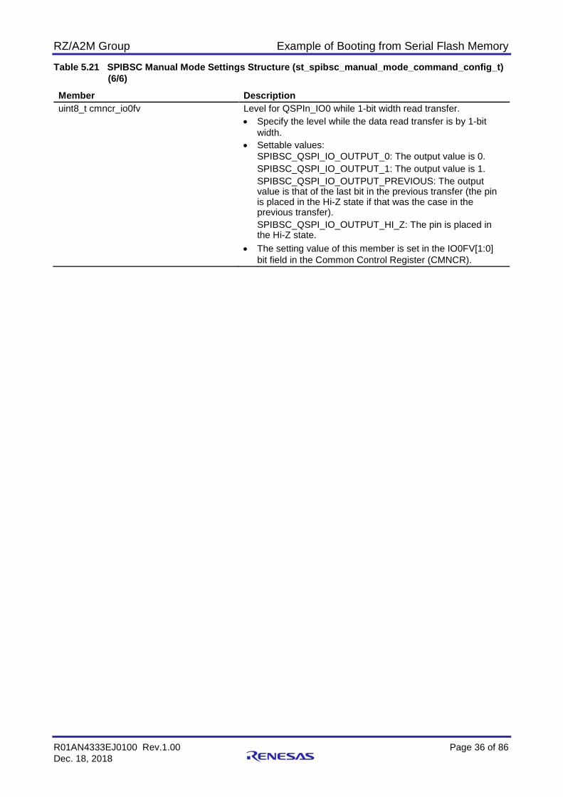
Table 5.21 SPIBSC Manual Mode Settings Structure (st_spibsc_manual_mode_command_config_t) (6/6)
Member Description uint8_t cmncr_io0fv Level for QSPIn_IO0 while 1-bit width read transfer.
• Specify the level while the data read transfer is by 1-bit width.
• Settable values: SPIBSC_QSPI_IO_OUTPUT_0: The output value is 0. SPIBSC_QSPI_IO_OUTPUT_1: The output value is 1. SPIBSC_QSPI_IO_OUTPUT_PREVIOUS: The output value is that of the last bit in the previous transfer (the pin is placed in the Hi-Z state if that was the case in the previous transfer). SPIBSC_QSPI_IO_OUTPUT_HI_Z: The pin is placed in the Hi-Z state.
• The setting value of this member is set in the IO0FV[1:0] bit field in the Common Control Register (CMNCR).
RZ/A2M Group Example of Booting from Serial Flash Memory
R01AN4333EJ0100 Rev.1.00 Page 37 of 86 Dec. 18, 2018
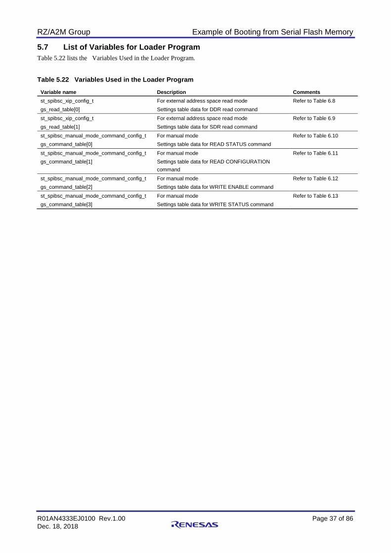
5.7 List of Variables for Loader Program Table 5.22 lists the Variables Used in the Loader Program.
Table 5.22 Variables Used in the Loader Program
Variable name Description Comments st_spibsc_xip_config_t gs_read_table[0]
For external address space read mode Settings table data for DDR read command
Refer to Table 6.8
st_spibsc_xip_config_t gs_read_table[1]
For external address space read mode Settings table data for SDR read command
Refer to Table 6.9
st_spibsc_manual_mode_command_config_t gs_command_table[0]
For manual mode Settings table data for READ STATUS command
Refer to Table 6.10
st_spibsc_manual_mode_command_config_t gs_command_table[1]
For manual mode Settings table data for READ CONFIGURATION command
Refer to Table 6.11
st_spibsc_manual_mode_command_config_t gs_command_table[2]
For manual mode Settings table data for WRITE ENABLE command
Refer to Table 6.12
st_spibsc_manual_mode_command_config_t gs_command_table[3]
For manual mode Settings table data for WRITE STATUS command
Refer to Table 6.13
RZ/A2M Group Example of Booting from Serial Flash Memory
R01AN4333EJ0100 Rev.1.00 Page 38 of 86 Dec. 18, 2018
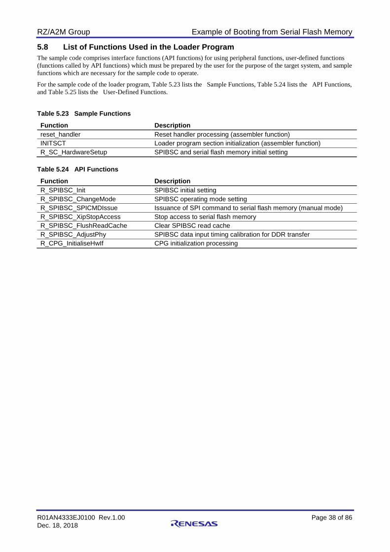
5.8 List of Functions Used in the Loader Program The sample code comprises interface functions (API functions) for using peripheral functions, user-defined functions (functions called by API functions) which must be prepared by the user for the purpose of the target system, and sample functions which are necessary for the sample code to operate.
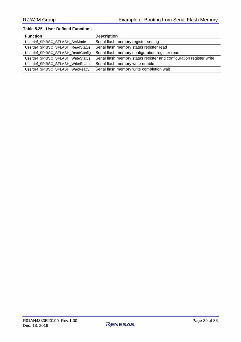
For the sample code of the loader program, Table 5.23 lists the Sample Functions, Table 5.24 lists the API Functions, and Table 5.25 lists the User-Defined Functions.
Table 5.23 Sample Functions
Function Description reset_handler Reset handler processing (assembler function) INITSCT Loader program section initialization (assembler function) R_SC_HardwareSetup SPIBSC and serial flash memory initial setting
Table 5.24 API Functions
Function Description R_SPIBSC_Init SPIBSC initial setting R_SPIBSC_ChangeMode SPIBSC operating mode setting R_SPIBSC_SPICMDIssue Issuance of SPI command to serial flash memory (manual mode) R_SPIBSC_XipStopAccess Stop access to serial flash memory R_SPIBSC_FlushReadCache Clear SPIBSC read cache R_SPIBSC_AdjustPhy SPIBSC data input timing calibration for DDR transfer R_CPG_InitialiseHwIf CPG initialization processing
RZ/A2M Group Example of Booting from Serial Flash Memory
R01AN4333EJ0100 Rev.1.00 Page 39 of 86 Dec. 18, 2018
Table 5.25 User-Defined Functions
Function Description Userdef_SPIBSC_SFLASH_SetMode Serial flash memory register setting Userdef_SPIBSC_SFLASH_ReadStatus Serial flash memory status register read Userdef_SPIBSC_SFLASH_ReadConfig Serial flash memory configuration register read Userdef_SPIBSC_SFLASH_WriteStatus Serial flash memory status register and configuration register write Userdef_SPIBSC_SFLASH_WriteEnable Serial flash memory write enable Userdef_SPIBSC_SFLASH_WaitReady Serial flash memory write completion wait

RZ/A2M Group Example of Booting from Serial Flash Memory
R01AN4333EJ0100 Rev.1.00 Page 40 of 86 Dec. 18, 2018
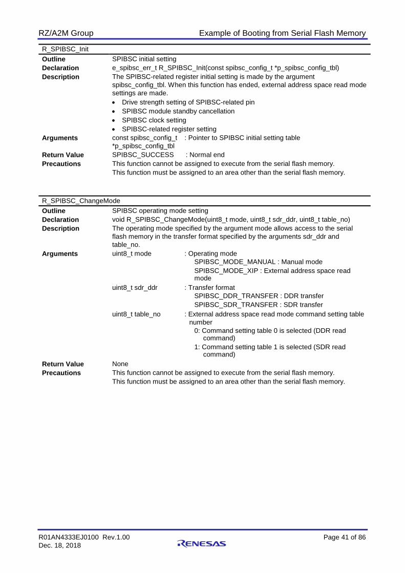
5.9 Function Specification Specifications of the functions of the sample code loader program are listed below.
reset_handler Outline Loader program reset handler Declaration reset_handler Description The entry function of the loader program. Arguments None Return Value None
INITSCT Outline Loader program section initialization Declaration void INITSCT(void) Description Transfers loader program processing that must be run on the large-capacity on-chip
RAM to the large-capacity on-chip RAM. Arguments p_dtbl : Pointer to the area where the loader program code,
constant data, and data with initial values that needs to be assigned to the large-capacity on-chip RAM is stored
p_btbl : Pointer to the area where the data with no initial values is stored
Return Value None R_SC_HardwareSetup Outline SPIBSC and serial flash memory initial setting Declaration void R_SC_HardwareSetup(void) Description Makes the optimal settings for the used serial flash memory, sets the SPIBSC to
external address space read mode, and accesses the serial flash memory. The following settings are made in the sample code. • Change to read command: H'03→H'EE • Serial flash memory register setting
Status register: QE bit set to 1 Configuration register: DC[1:0] and ODS[2:0] bit settings (The DC[1:0] bit setting differs depending on the read command. Refer to "Table 6.5 List of numbers of dummy cycles necessary for the operating frequency of the MX25L51245GXD".)
• Change to QSPIn_SPCLK operating frequency: P0ϕ/2→Bϕ/2 Arguments None Return Value None Precautions This function cannot be assigned to execute from the serial flash memory.
This function must be assigned to an area other than the serial flash memory.
RZ/A2M Group Example of Booting from Serial Flash Memory
R01AN4333EJ0100 Rev.1.00 Page 41 of 86 Dec. 18, 2018
R_SPIBSC_Init Outline SPIBSC initial setting Declaration e_spibsc_err_t R_SPIBSC_Init(const spibsc_config_t *p_spibsc_config_tbl) Description The SPIBSC-related register initial setting is made by the argument
spibsc_config_tbl. When this function has ended, external address space read mode settings are made. • Drive strength setting of SPIBSC-related pin • SPIBSC module standby cancellation • SPIBSC clock setting • SPIBSC-related register setting
Arguments const spibsc_config_t *p_spibsc_config_tbl
: Pointer to SPIBSC initial setting table
Return Value SPIBSC_SUCCESS : Normal end Precautions This function cannot be assigned to execute from the serial flash memory.
This function must be assigned to an area other than the serial flash memory. R_SPIBSC_ChangeMode Outline SPIBSC operating mode setting Declaration void R_SPIBSC_ChangeMode(uint8_t mode, uint8_t sdr_ddr, uint8_t table_no) Description The operating mode specified by the argument mode allows access to the serial
flash memory in the transfer format specified by the arguments sdr_ddr and table_no.
Arguments uint8_t mode : Operating mode SPIBSC_MODE_MANUAL : Manual mode SPIBSC_MODE_XIP : External address space read mode
uint8_t sdr_ddr : Transfer format SPIBSC_DDR_TRANSFER : DDR transfer SPIBSC_SDR_TRANSFER : SDR transfer
uint8_t table_no : External address space read mode command setting table number
0: Command setting table 0 is selected (DDR read command)
1: Command setting table 1 is selected (SDR read command)
Return Value None Precautions This function cannot be assigned to execute from the serial flash memory.
This function must be assigned to an area other than the serial flash memory.
RZ/A2M Group Example of Booting from Serial Flash Memory
R01AN4333EJ0100 Rev.1.00 Page 42 of 86 Dec. 18, 2018
R_SPIBSC_SPICMDIssue Outline Issuance of SPI command to serial flash memory (for manual mode) Declaration spibsc_err_t R_SPIBSC_SPICMDIssue(uint8_t table_no, uint32_t addr,
uint8_t *write_buff, uint32_t write_size, uint8_t *read_buff, uint32_t read_size) Description Uses the configuration table for issuing SPI commands specified by the argument
table_no to issue SPI commands. According to the contents of table_no, when a write command is issued, the data stored in the argument *write_buff is written, at the number of bytes specified by the argument write_size from the address specified by the argument addr. When a read command is issued, the data is read at the number of bytes specified by the argument read_size from the address specified by the argument addr, and stored in the area specified by the argument *read_buff.
Arguments uint8_t table_no : The table storing the setting information for the command used
uint32_t addr : Address uint8_t * write_buff : Write buffer pointer uint32_t write_size : Number of bytes written uint8_t * read_buff : Read buffer pointer uint32_t read_size : Number of bytes read Return Value SPIBSC_SUCCESS : Normal end Precautions This function cannot be assigned to execute from the serial flash memory.
This function must be assigned to an area other than the serial flash memory. R_SPIBSC_XipStopAccess Outline Stop access to serial flash memory Declaration void R_SPIBSC_XipStopAccess( void ) Description Negates QSPIn_SSL with external address space read mode and stops access to
the serial flash memory. When SPIBSC-related register settings are being made, this function is called so that the serial flash memory is not accessed.
Arguments None Return Value None Precautions This function cannot be assigned to execute from the serial flash memory.
This function must be assigned to an area other than the serial flash memory. R_SPIBSC_FlushReadCache Outline Clear SPIBSC read cache Declaration void R_SPIBSC_FlushReadCache( void ) Description Clears the SPIBSC read cache. Arguments None Return Value None Precautions This function cannot be assigned to execute from the serial flash memory.
This function must be assigned to an area other than the serial flash memory.
RZ/A2M Group Example of Booting from Serial Flash Memory
R01AN4333EJ0100 Rev.1.00 Page 43 of 86 Dec. 18, 2018
R_SPIBSC_AdjustPhy Outline SPIBSC data input timing calibration for DDR transfer Declaration e_spibsc_err_t R_SPIBSC_AdjustPhy(void) Description Calibrates the data input timing from the serial flash memory.
Adjusts the input data input timing so that 4-byte data stored in the flash memory can be correctly read. 4-byte data is stored in the address defined by the g_spibsc_test_pattern symbol. Call this function before accessing to the serial flash memory by DDR transfer.
Arguments None Return Value SPIBSC_SUCCESS : Normal end
SPIBSC_ERR_INVALID : Abnormal end Precautions • Do not call this function if any devices other than the serial flash memory are
connected to the SPIBSC. • The g_spibsc_test_pattern constant data area used in this function must be
assigned to the serial flash memory. • This function cannot be assigned to execute from the serial flash memory.
This function must be assigned to an area other than the serial flash memory. • Use this function when set to manual mode.
R_CPG_InitialiseHwIf Outline CPC initialization processing Declaration int_t R_CPG_InitialiseHwIf( void ) Description Uses the r_cpg_drv_sc_cfg.h CPG configuration data to make CPG register
(FRQCR, CKIOSEL, SCLKSEL) settings. In this sample code, CPG settings are made so that the operating frequency in "Operating clock settings" and "SPIBSC clock selection" in "Table 5.4 Settings for the boot startup on-chip ROM program and loader program (3/3)" is used.
Arguments None None Return Value DRV_SUCCESS : Normal end
DRV_ERROR : r_cpg_drv_sc_cfg.h CPG configuration data is wrong Precautions This function must be assigned to the large-capacity on-chip RAM.
RZ/A2M Group Example of Booting from Serial Flash Memory
R01AN4333EJ0100 Rev.1.00 Page 44 of 86 Dec. 18, 2018
Userdef_SPIBSC_SFLASH_SetMode Outline Serial flash memory register setting Declaration void Userdef_SPIBSC_SFLASH_SetMode(uint8_t mode, uint8_t sdr_ddr) Description Implement a processing that sets to the serial flash memory registers so that access
is possible in the transfer format specified by the argument sdr_ddr via access at the bit width specified by the argument mode, according to the specifications of the serial flash memory to be used. In the sample code, MX25L51245GXD register settings are made and access is set via DDR transfer at 4-bit width.
Arguments uint8_t mode : Operating mode SPIBSC_QE_DISABLE: Single mode (bit width: 1 bit) SPIBSC_QE_ENABLE: Quad mode (bit width: 4 bits)
uint8_t sdr_ddr : Transfer format SPIBSC_DDR_TRANSFER : DDR transfer SPIBSC_SDR_TRANSFER : SDR transfer
Return Value None Precautions This function cannot be assigned to execute from the serial flash memory.
This function must be assigned to an area other than the serial flash memory. Userdef_SPIBSC_SFLASH_ReadStatus Outline Serial flash memory status register read Declaration void Userdef_SPIBSC_SFLASH_ReadStatus(uint8_t *p_status) Description Implement a processing to read the serial flash memory status register and to store
the data read with the argument *p_status, according to the specifications of the serial flash memory to be used. In the sample code, a processing to read the status register of MX25L51245GXD is performed.
Arguments uint8_t *p_status : The value read from the status register Return Value None Precautions This function cannot be assigned to execute from the serial flash memory.
This function must be assigned to an area other than the serial flash memory. Userdef_SPIBSC_SFLASH_ReadConfig Outline Serial flash memory configuration register read Declaration void Userdef_SPIBSC_SFLASH_ReadConfig(uint8_t *p_config) Description Implement a processing to read the serial flash memory configuration register and to
store the data read with the argument *p_config, according to the specifications of the serial flash memory to be used. In the sample code, a processing to read the configuration register of MX25L51245GXD is performed.
Arguments uint8_t *p_config : The value read from the configuration register Return Value None Precautions This function cannot be assigned to execute from the serial flash memory.
This function must be assigned to an area other than the serial flash memory.
RZ/A2M Group Example of Booting from Serial Flash Memory
R01AN4333EJ0100 Rev.1.00 Page 45 of 86 Dec. 18, 2018
Userdef_SPIBSC_SFLASH_WriteStatus Outline Serial flash memory status register and configuration register write Declaration void Userdef_SPIBSC_SFLASH_WriteStatus(uint8_t *p_status, uint8_t *p_config) Description Implement a processing that sets the values specified by the arguments *p_status
and *p_config to the serial flash memory status register and configuration register respectively, according to the specifications of the serial flash memory to be used. In the sample code, a processing to read the status register and configuration register of MX25L51245GXD is performed.
Arguments uint8_t *p_status : Setting in status register uint8_t *p_config : Setting in config register Return Value None Precautions This function cannot be assigned to execute from the serial flash memory.
This function must be assigned to an area other than the serial flash memory. Userdef_SPIBSC_SFLASH_WriteEnable Outline Serial flash memory write enable Declaration void Userdef_SPIBSC_SFLASH_WriteEnable(void) Description Implement the processing that enables the serial flash memory registers for writes,
according to the specifications of the serial flash memory to be used. In the sample code, processing to issue "Write Status Register (WRSR)" commands to MX25L51245GXD is performed.
Arguments None Return Value None Precautions This function cannot be assigned to execute from the serial flash memory.
This function must be assigned to an area other than the serial flash memory. Userdef_SPIBSC_SFLASH_WaitReady Outline Serial flash memory write completion wait Declaration void Userdef_SPIBSC_SFLASH_WaitReady(void) Description Implement the processing that waits for the write to the serial flash memory to be
completed, according to the specifications of the serial flash memory to be used. In the sample code, processing to issue "Read Status Register (RDSR)" commands to MX25L51245GXD and to wait for the write to be completed is performed by referencing the status register contents.
Arguments None Return Value None Precautions This function cannot be assigned to execute from the serial flash memory.
This function must be assigned to an area other than the serial flash memory.
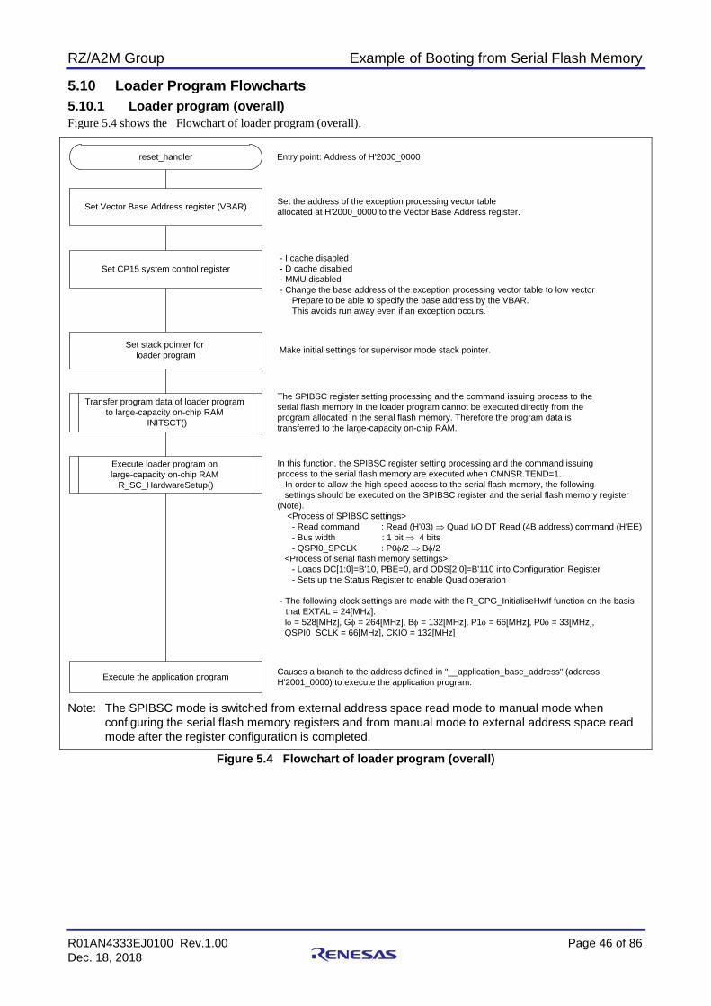
RZ/A2M Group Example of Booting from Serial Flash Memory
R01AN4333EJ0100 Rev.1.00 Page 46 of 86 Dec. 18, 2018
5.10 Loader Program Flowcharts 5.10.1 Loader program (overall) Figure 5.4 shows the Flowchart of loader program (overall).
Note: The SPIBSC mode is switched from external address space read mode to manual mode when
configuring the serial flash memory registers and from manual mode to external address space read mode after the register configuration is completed.
Figure 5.4 Flowchart of loader program (overall)
- I cache disabled - D cache disabled - MMU disabled - Change the base address of the exception processing vector table to low vector Prepare to be able to specify the base address by the VBAR. This avoids run away even if an exception occurs.
Entry point: Address of H'2000_0000
The SPIBSC register setting processing and the command issuing process to the serial flash memory in the loader program cannot be executed directly from the program allocated in the serial flash memory. Therefore the program data is transferred to the large-capacity on-chip RAM.
In this function, the SPIBSC register setting processing and the command issuingprocess to the serial flash memory are executed when CMNSR.TEND=1. - In order to allow the high speed access to the serial flash memory, the following settings should be executed on the SPIBSC register and the serial flash memory register (Note). <Process of SPIBSC settings> - Read command : Read (H'03) ⇒ Quad I/O DT Read (4B address) command (H'EE) - Bus width : 1 bit ⇒ 4 bits - QSPI0_SPCLK : P0φ/2 ⇒ Bφ/2 <Process of serial flash memory settings> - Loads DC[1:0]=B'10, PBE=0, and ODS[2:0]=B'110 into Configuration Register - Sets up the Status Register to enable Quad operation
- The following clock settings are made with the R_CPG_InitialiseHwIf function on the basis that EXTAL = 24[MHz]. Iφ = 528[MHz], Gφ = 264[MHz], Bφ = 132[MHz], P1φ = 66[MHz], P0φ = 33[MHz], QSPI0_SCLK = 66[MHz], CKIO = 132[MHz]
Execute the application program Causes a branch to the address defined in "__application_base_address" (address H'2001_0000) to execute the application program.
Make initial settings for supervisor mode stack pointer.
Set the address of the exception processing vector tableallocated at H'2000_0000 to the Vector Base Address register.
Set CP15 system control register
reset_handler
Transfer program data of loader programto large-capacity on-chip RAM
INITSCT()
Execute loader program onlarge-capacity on-chip RAM
R_SC_HardwareSetup()
Set stack pointer forloader program
Set Vector Base Address register (VBAR)
RZ/A2M Group Example of Booting from Serial Flash Memory
R01AN4333EJ0100 Rev.1.00 Page 47 of 86 Dec. 18, 2018
5.10.2 SPIBSC and Serial Flash Memory Initial Setting The loader program sets up the serial flash memory registers (QE bit of the status register, and DC[1:0] bits, PBE bit, and ODS[2:0] bits of the configuration register) and changes the bus bit width from 1 bit to 4 bits so that the serial flash memory can be accessed at a higher speed. After setting up the serial flash memory registers, the program sets the type of read command to be issued to the serial flash memory when using the SPIBSC in external address space read mode to "Quad I/O DT Read (4B address)" (H'EE) and changes the SPI clock frequency to Bϕ/2.
Since the loader program modifies the SPIBSC registers during its processing, it cannot run in the SPI multi-I/O bus space. Accordingly, it is transferred in large-capacity on-chip RAM for execution.
Figure 5.5 shows the flowchart of the loader program, and Figure 5.6 to Figure 5.18 show the flowcharts of the used functions.
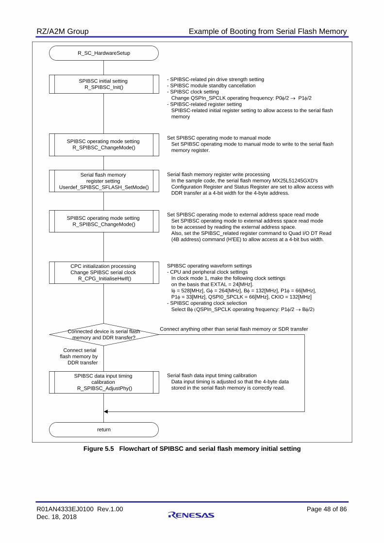
RZ/A2M Group Example of Booting from Serial Flash Memory
R01AN4333EJ0100 Rev.1.00 Page 48 of 86 Dec. 18, 2018
Figure 5.5 Flowchart of SPIBSC and serial flash memory initial setting
R_SC_HardwareSetup
return
SPIBSC operating mode settingR_SPIBSC_ChangeMode()
CPC initialization processingChange SPIBSC serial clock
R_CPG_InitialiseHwIf()
SPIBSC operating mode settingR_SPIBSC_ChangeMode()
SPIBSC initial settingR_SPIBSC_Init()
Serial flash memoryregister setting
Userdef_SPIBSC_SFLASH_SetMode()
SPIBSC data input timingcalibration
R_SPIBSC_AdjustPhy()
Connected device is serial flash memory and DDR transfer?
Connect serialflash memory by
DDR transfer
Connect anything other than serial flash memory or SDR transfer
- SPIBSC-related pin drive strength setting- SPIBSC module standby cancellation- SPIBSC clock setting Change QSPIn_SPCLK operating frequency: P0φ/2 → P1φ/2- SPIBSC-related register setting SPIBSC-related initial register setting to allow access to the serial flash memory
Set SPIBSC operating mode to manual mode Set SPIBSC operating mode to manual mode to write to the serial flash memory register.
Serial flash memory register write processing In the sample code, the serial flash memory MX25L51245GXD's Configuration Register and Status Register are set to allow access with DDR transfer at a 4-bit width for the 4-byte address.
Set SPIBSC operating mode to external address space read mode Set SPIBSC operating mode to external address space read mode to be accessed by reading the external address space. Also, set the SPIBSC_related register command to Quad I/O DT Read (4B address) command (H'EE) to allow access at a 4-bit bus width.
SPIBSC operating waveform settings- CPU and peripheral clock settings In clock mode 1, make the following clock settings on the basis that EXTAL = 24[MHz]. Iφ = 528[MHz], Gφ = 264[MHz], Bφ = 132[MHz], P1φ = 66[MHz], P1φ = 33[MHz], QSPI0_SPCLK = 66[MHz], CKIO = 132[MHz]- SPIBSC operating clock selection Select Bφ (QSPIn_SPCLK operating frequency: P1φ/2 → Bφ/2)
Serial flash data input timing calibration Data input timing is adjusted so that the 4-byte data stored in the serial flash memory is correctly read.
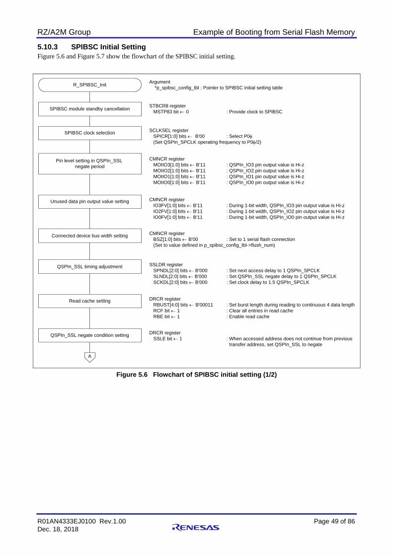
RZ/A2M Group Example of Booting from Serial Flash Memory
R01AN4333EJ0100 Rev.1.00 Page 49 of 86 Dec. 18, 2018
5.10.3 SPIBSC Initial Setting Figure 5.6 and Figure 5.7 show the flowchart of the SPIBSC initial setting.
Figure 5.6 Flowchart of SPIBSC initial setting (1/2)
R_SPIBSC_Init
Read cache setting
QSPIn_SSL timing adjustment
Argument *p_spibsc_config_tbl : Pointer to SPIBSC initial setting table
SPIBSC module standby cancellation
SPIBSC clock selection
Pin level setting in QSPIn_SSLnegate period
STBCR8 register MSTP83 bit ← 0 : Provide clock to SPIBSC
SCLKSEL register SPICR[1:0] bits ← B'00 : Select P0φ (Set QSPIn_SPCLK operating frequency to P0φ/2)
CMNCR register MOIIO3[1:0] bits ← B'11 : QSPIn_IO3 pin output value is Hi-z MOIIO2[1:0] bits ← B'11 : QSPIn_IO2 pin output value is Hi-z MOIIO1[1:0] bits ← B'11 : QSPIn_IO1 pin output value is Hi-z MOIIO0[1:0] bits ← B'11 : QSPIn_IO0 pin output value is Hi-z
SSLDR register SPNDL[2:0] bits ← B'000 : Set next access delay to 1 QSPIn_SPCLK SLNDL[2:0] bits ← B'000 : Set QSPIn_SSL negate delay to 1 QSPIn_SPCLK SCKDL[2:0] bits ← B'000 : Set clock delay to 1.5 QSPIn_SPCLK
DRCR register RBUST[4:0] bits ← B'00011 : Set burst length during reading to continuous 4 data length RCF bit ← 1 : Clear all entries in read cache RBE bit ← 1 : Enable read cache
A
Connected device bus width setting CMNCR register BSZ[1:0] bits ← B'00 : Set to 1 serial flash connection (Set to value defined in p_spibsc_config_tbl->flush_num)
QSPIn_SSL negate condition setting DRCR register SSLE bit ← 1 : When accessed address does not continue from previous transfer address, set QSPIn_SSL to negate
Unused data pin output value setting CMNCR register IO3FV[1:0] bits ← B'11 : During 1-bit width, QSPIn_IO3 pin output value is Hi-z IO2FV[1:0] bits ← B'11 : During 1-bit width, QSPIn_IO2 pin output value is Hi-z IO0FV[1:0] bits ← B'11 : During 1-bit width, QSPIn_IO0 pin output value is Hi-z
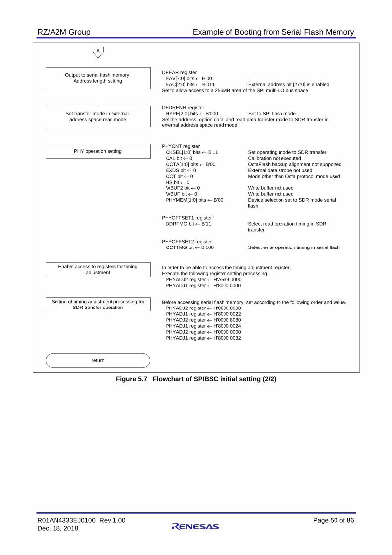
RZ/A2M Group Example of Booting from Serial Flash Memory
R01AN4333EJ0100 Rev.1.00 Page 50 of 86 Dec. 18, 2018
Figure 5.7 Flowchart of SPIBSC initial setting (2/2)
return
DREAR register EAV[7:0] bits ← H'00 EAC[2:0] bits ← B'011 : External address bit [27:0] is enabledSet to allow access to a 256MB area of the SPI multi-I/O bus space.
Output to serial flash memoryAddress length setting
Set transfer mode in externaladdress space read mode
PHY operation setting
A
DRDRENR register HYPE[2:0] bits ← B'000 : Set to SPI flash modeSet the address, option data, and read data transfer mode to SDR transfer in external address space read mode.
PHYCNT register CKSEL[1:0] bits ← B'11 : Set operating mode to SDR transfer CAL bit ← 0 : Calibration not executed OCTA[1:0] bits ← B'00 : OctaFlash backup alignment not supported EXDS bit ← 0 : External data strobe not used OCT bit ← 0 : Mode other than Octa protocol mode used HS bit ← 0 WBUF2 bit ← 0 : Write buffer not used WBUF bit ← 0 : Write buffer not used PHYMEM[1:0] bits ← B'00 : Device selection set to SDR mode serial flash
PHYOFFSET1 register DDRTMG bit ← B'11 : Select read operation timing in SDR transfer
PHYOFFSET2 register OCTTMG bit ← B'100 : Select write operation timing in serial flash
Enable access to registers for timing adjustment
In order to be able to access the timing adjustment register,Execute the following register setting processing. PHYADJ2 register ← H'A539 0000 PHYADJ1 register ← H'8000 0000
Before accessing serial flash memory, set according to the following order and value. PHYADJ2 register ← H'0000 8080 PHYADJ1 register ← H'8000 0022 PHYADJ2 register ← H'0000 8080 PHYADJ1 register ← H'8000 0024 PHYADJ2 register ← H'0000 0000 PHYADJ1 register ← H'8000 0032
Setting of timing adjustment processing for SDR transfer operation

RZ/A2M Group Example of Booting from Serial Flash Memory
R01AN4333EJ0100 Rev.1.00 Page 51 of 86 Dec. 18, 2018
5.10.4 SPIBSC Operating Mode Setting Figure 5.8 to Figure 5.10 show the SPIBSC operating mode setting.
Figure 5.8 Flowchart of SPIBSC operating mode setting (1/3)
R_SPIBSC_ChangeMode Argument mode: Operating mode SPIBSC_MODE_MANUAL : Manual operating mode SPIBSC_MODE_XIP : External address space read mode sdr_ddr: Transfer format SPIBSC_SDR_TRANSFER : SDR transfer SPIBSC_DDR_TRANSFER : DDR transfer table_no: Table number for external address space read 0 : DDR transfer table 1 : SDR transfer table
Operating mode?(mode)
External address space read mode
Table pointer setting for serial flash memory external address space read p_xip_cmd_tbl ← &gs_xip_read_table[table_no]
Table pointer setting for external address space read
A
Shared control register(CMNCR) setting MD bit ← 0 : Sets to external address space read mode
PHYMEM[1:0] bits ← B'01 : Sets device selection to DDR mode serial flash
DDRTMG[1:0] bits ← B'10 : Sets adjustment timing based on DDR read operation
OCTTMG[2:0] bits ← B'100 : Selects either serial flash or HyperFlash write timing adjustment
Transfer format?(sdr_ddr)
PHY control register(PHYCNT) setting
PHY offset 1 register(PHYOFFSET1) setting
PHY offset 2 register(PHYOFFSET2) setting
PHYMEM[1:0] bits ← B'00 : Sets device selection to SDR mode serial flash
DDRTMG[1:0] bits ← B'11 : Sets adjustment timing based on SDR read operation
OCTTMG[2:0] bits ← B'100 : Selects either serial flash or HyperFlash write timing adjustment
DDR transfer (SPIBSC_DDR_TRANSFER)
SDR transfer (SPIBSC_SDR_TRANSFER)
B
PHY control register(PHYCNT) setting
PHY offset 1 register(PHYOFFSET1) setting
PHY offset 2 register(PHYOFFSET2) setting
Manual operating mode

RZ/A2M Group Example of Booting from Serial Flash Memory
R01AN4333EJ0100 Rev.1.00 Page 52 of 86 Dec. 18, 2018
Figure 5.9 Flowchart of SPIBSC operating mode setting (2/3)
External address space read modecommand setting
External address space read modeoptional command setting
External address space read modeaddress setting
External address space read modeoption data setting
External address space read modedummy cycle setting
External address space read modetransfer data setting
DRCMR register CMD[7:0] bits ← p_xip_cmd_tbl->cmd : Command code settingDRENR register CDB[1:0] bits ← p_xip_cmd_tbl->cmd_width : Command bit width setting CDE bit ← p_xip_cmd_tbl->cmd_output_enable : Command output enable/disable setting
B
External address space read mode
A
C D
Manual mode
DRCMR register OCMD[7:0] bits ← p_xip_cmd_tbl->ocmd : Optional command code settingDRENR register OCDB[1:0] bits ← p_xip_cmd_tbl->ocmd_width : Optional command bit width setting OCDE bit ← p_xip_cmd_tbl->ocmd_output_enable : Optional command output enable/disable setting
DRENR register ADB[1:0] bits ← p_xip_cmd_tbl->addr_width : Address bit width setting ADE[3:0] bits ← p_xip_cmd_tbl->addr_output_enable : Address output method settingDRDRENR register ADDRE bit ← p_xip_cmd_tbl->addr_ddr_enable : Address transfer format setting
DROPR register OPD3[7:0] bits ← p_xip_cmd_tbl->opd3 : Option data 3 setting OPD2[7:0] bits ← p_xip_cmd_tbl->opd2 : Option data 2 setting OPD1[7:0] bits ← p_xip_cmd_tbl->opd1 : Option data 1 setting OPD0[7:0] bits ← p_xip_cmd_tbl->opd0 : Option data 0 settingDRENR register OPDB[1:0] bits ← p_xip_cmd_tbl->opdata_width : Option data bit width setting OPDE[3:0] bits ← p_xip_cmd_tbl->opdata_output_enable : Option data output method settingDRDRENR register OPDRE bit ← p_xip_cmd_tbl->opdata_ddr_enable : Option data transfer format setting
DRDMCR register DMCYC[4:0] bits ← p_xip_cmd_tbl->dummy_cycle_count : Number of dummy cycles settingDRENR register DME bit ← p_xip_cmd_tbl->dummy_cycle_enable : Dummy cycle insertion enable/disable setting
DRENR register DRDB[1:0] bits ← p_xip_cmd_tbl->data_width : Data read bit width settingDRDRENR register DRDRE bit ← p_xip_cmd_tbl->data_ddr_enable : Data read transfer format setting
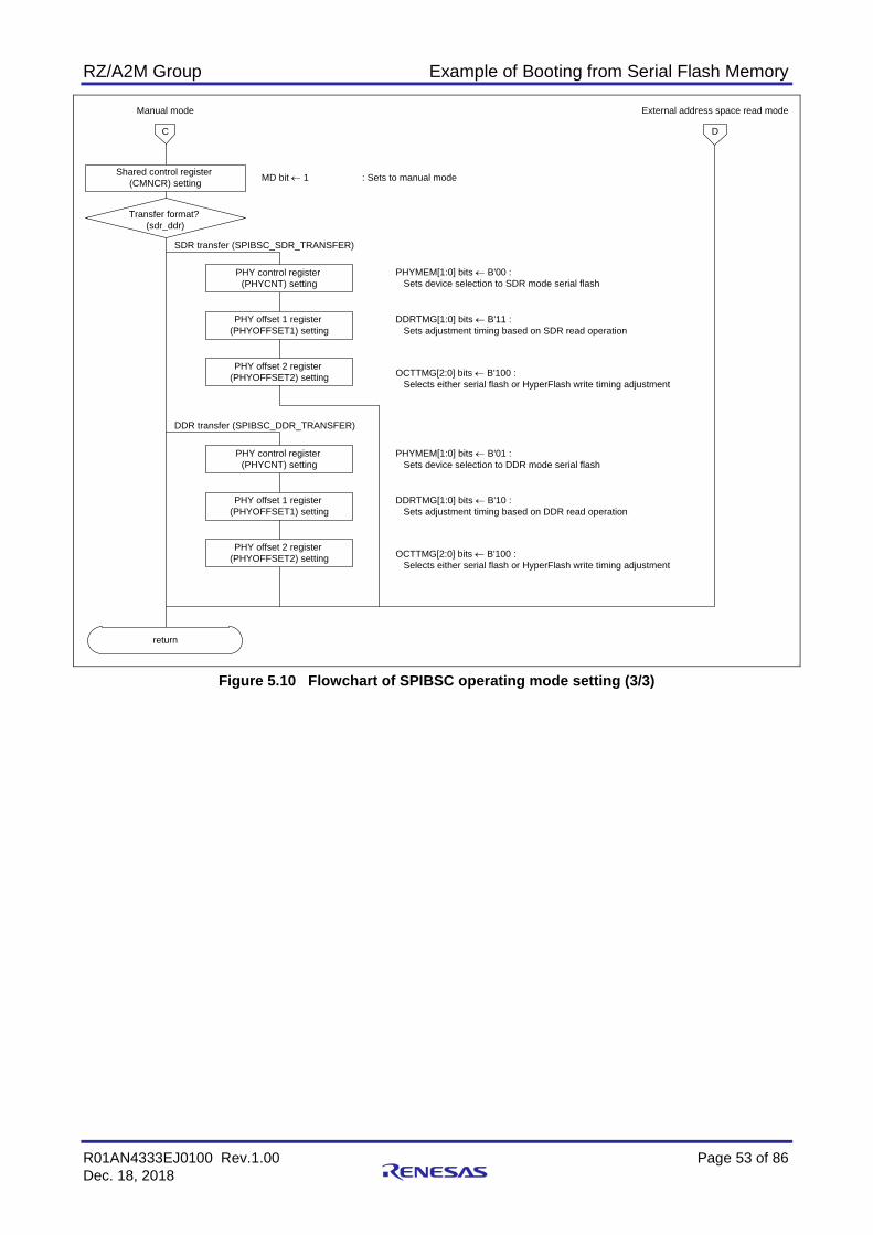
RZ/A2M Group Example of Booting from Serial Flash Memory
R01AN4333EJ0100 Rev.1.00 Page 53 of 86 Dec. 18, 2018
Figure 5.10 Flowchart of SPIBSC operating mode setting (3/3)
return
Manual mode
C D
Shared control register(CMNCR) setting MD bit ← 1 : Sets to manual mode
PHYMEM[1:0] bits ← B'01 : Sets device selection to DDR mode serial flash
DDRTMG[1:0] bits ← B'10 : Sets adjustment timing based on DDR read operation
OCTTMG[2:0] bits ← B'100 : Selects either serial flash or HyperFlash write timing adjustment
Transfer format?(sdr_ddr)
PHY control register(PHYCNT) setting
PHY offset 1 register(PHYOFFSET1) setting
PHY offset 2 register(PHYOFFSET2) setting
PHYMEM[1:0] bits ← B'00 : Sets device selection to SDR mode serial flash
DDRTMG[1:0] bits ← B'11 : Sets adjustment timing based on SDR read operation
OCTTMG[2:0] bits ← B'100 : Selects either serial flash or HyperFlash write timing adjustment
DDR transfer (SPIBSC_DDR_TRANSFER)
SDR transfer (SPIBSC_SDR_TRANSFER)
PHY control register(PHYCNT) setting
PHY offset 1 register(PHYOFFSET1) setting
PHY offset 2 register(PHYOFFSET2) setting
External address space read mode
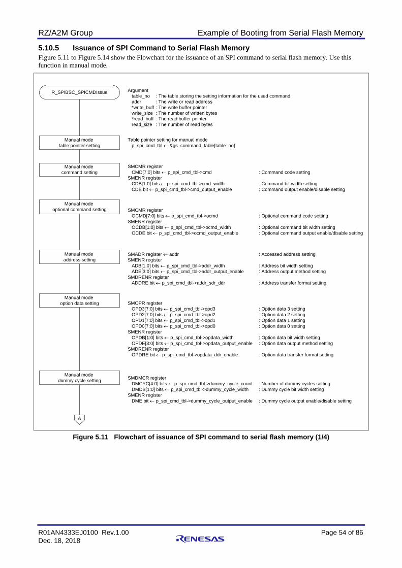
RZ/A2M Group Example of Booting from Serial Flash Memory
R01AN4333EJ0100 Rev.1.00 Page 54 of 86 Dec. 18, 2018
5.10.5 Issuance of SPI Command to Serial Flash Memory Figure 5.11 to Figure 5.14 show the Flowchart for the issuance of an SPI command to serial flash memory. Use this function in manual mode.
Figure 5.11 Flowchart of issuance of SPI command to serial flash memory (1/4)
R_SPIBSC_SPICMDIssue
A
Argument table_no : The table storing the setting information for the used command addr : The write or read address *write_buff : The write buffer pointer write_size : The number of written bytes *read_buff : The read buffer pointer read_size : The number of read bytes
Manual modecommand setting
Table pointer setting for manual mode p_spi_cmd_tbl ← &gs_command_table[table_no]
Manual modetable pointer setting
Manual modeoptional command setting
Manual modeaddress setting
Manual modeoption data setting
Manual modedummy cycle setting
SMCMR register CMD[7:0] bits ← p_spi_cmd_tbl->cmd : Command code settingSMENR register CDB[1:0] bits ← p_spi_cmd_tbl->cmd_width : Command bit width setting CDE bit ← p_spi_cmd_tbl->cmd_output_enable : Command output enable/disable setting
SMCMR register OCMD[7:0] bits ← p_spi_cmd_tbl->ocmd : Optional command code settingSMENR register OCDB[1:0] bits ← p_spi_cmd_tbl->ocmd_width : Optional command bit width setting OCDE bit ← p_spi_cmd_tbl->ocmd_output_enable : Optional command output enable/disable setting
SMADR register ← addr : Accessed address settingSMENR register ADB[1:0] bits ← p_spi_cmd_tbl->addr_width : Address bit width setting ADE[3:0] bits ← p_spi_cmd_tbl->addr_output_enable : Address output method settingSMDRENR register ADDRE bit ← p_spi_cmd_tbl->addr_sdr_ddr : Address transfer format setting
SMOPR register OPD3[7:0] bits ← p_spi_cmd_tbl->opd3 : Option data 3 setting OPD2[7:0] bits ← p_spi_cmd_tbl->opd2 : Option data 2 setting OPD1[7:0] bits ← p_spi_cmd_tbl->opd1 : Option data 1 setting OPD0[7:0] bits ← p_spi_cmd_tbl->opd0 : Option data 0 settingSMENR register OPDB[1:0] bits ← p_spi_cmd_tbl->opdata_width : Option data bit width setting OPDE[3:0] bits ← p_spi_cmd_tbl->opdata_output_enable : Option data output method settingSMDRENR register OPDRE bit ← p_spi_cmd_tbl->opdata_ddr_enable : Option data transfer format setting
SMDMCR register DMCYC[4:0] bits ← p_spi_cmd_tbl->dummy_cycle_count : Number of dummy cycles setting DMDB[1:0] bits ← p_spi_cmd_tbl->dummy_cycle_width : Dummy cycle bit width settingSMENR register DME bit ← p_spi_cmd_tbl->dummy_cycle_output_enable : Dummy cycle output enable/disable setting
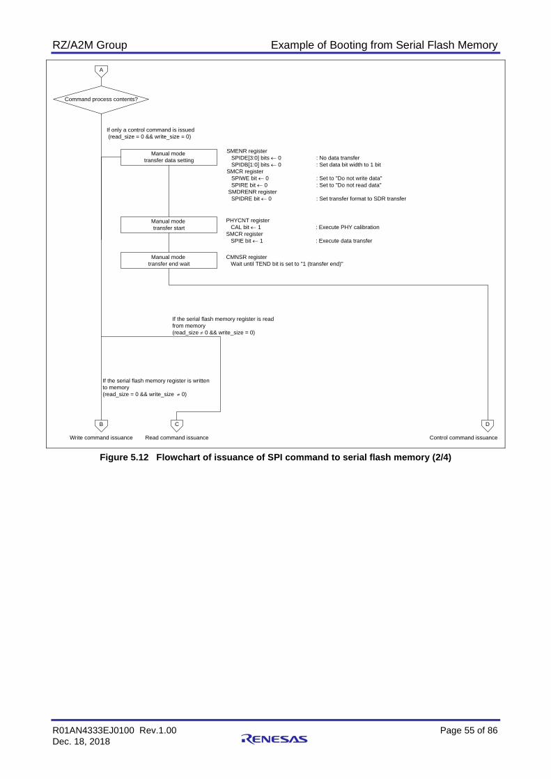
RZ/A2M Group Example of Booting from Serial Flash Memory
R01AN4333EJ0100 Rev.1.00 Page 55 of 86 Dec. 18, 2018
Figure 5.12 Flowchart of issuance of SPI command to serial flash memory (2/4)
Command process contents?
If only a control command is issued (read_size = 0 && write_size = 0)
If the serial flash memory register is readfrom memory(read_size ≠ 0 && write_size = 0)
If the serial flash memory register is writtento memory(read_size = 0 && write_size ≠ 0)
A
Manual modetransfer data setting
Manual modetransfer start
PHYCNT register CAL bit ← 1 : Execute PHY calibrationSMCR register SPIE bit ← 1 : Execute data transfer
Manual modetransfer end wait
B C D
Write command issuance Read command issuance Control command issuance
SMENR register SPIDE[3:0] bits ← 0 : No data transfer SPIDB[1:0] bits ← 0 : Set data bit width to 1 bitSMCR register SPIWE bit ← 0 : Set to "Do not write data" SPIRE bit ← 0 : Set to "Do not read data"SMDRENR register SPIDRE bit ← 0 : Set transfer format to SDR transfer
CMNSR register Wait until TEND bit is set to "1 (transfer end)"
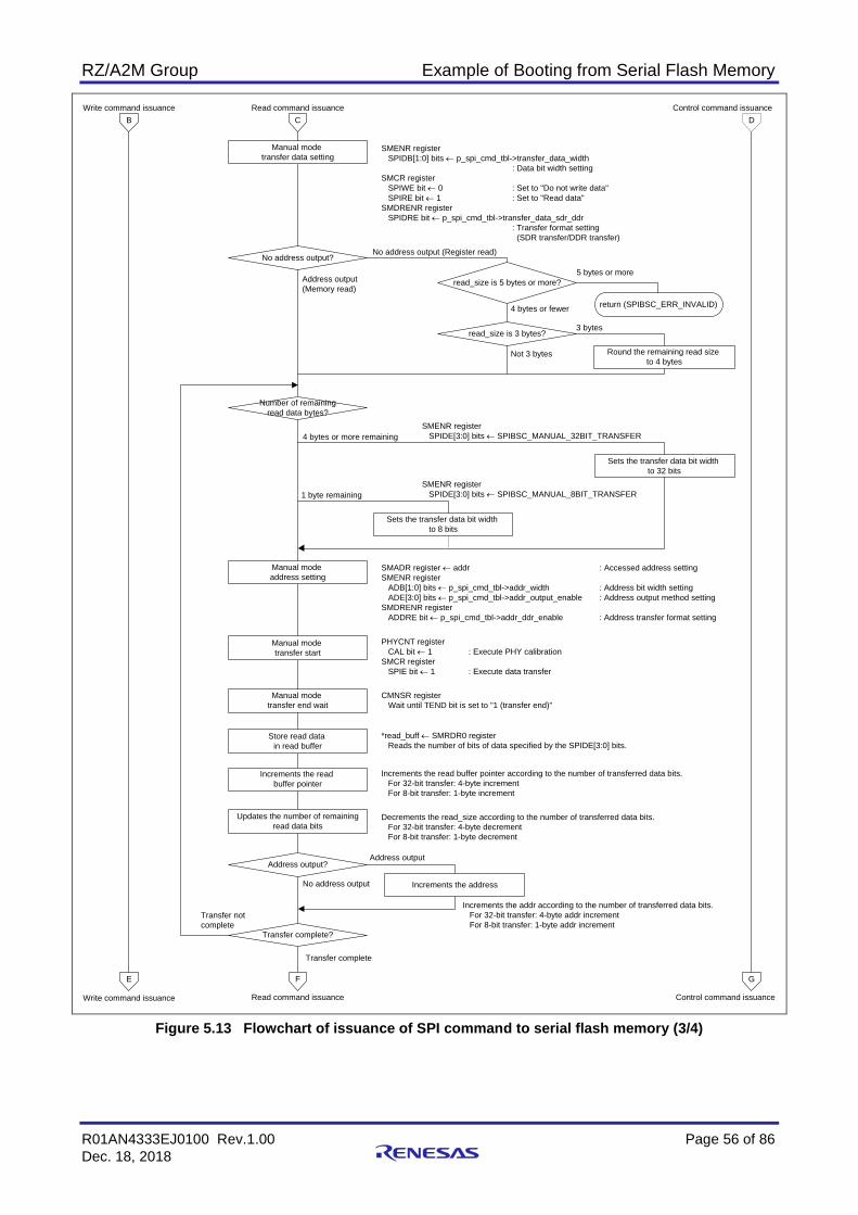
RZ/A2M Group Example of Booting from Serial Flash Memory
R01AN4333EJ0100 Rev.1.00 Page 56 of 86 Dec. 18, 2018
Figure 5.13 Flowchart of issuance of SPI command to serial flash memory (3/4)
Manual modetransfer data setting
Manual modetransfer start
PHYCNT register CAL bit ← 1 : Execute PHY calibrationSMCR register SPIE bit ← 1 : Execute data transfer
Manual modetransfer end wait
CMNSR register Wait until TEND bit is set to "1 (transfer end)"
Store read datain read buffer
Transfer complete?
Transfer not complete
Manual modeaddress setting
SMADR register ← addr : Accessed address settingSMENR register ADB[1:0] bits ← p_spi_cmd_tbl->addr_width : Address bit width setting ADE[3:0] bits ← p_spi_cmd_tbl->addr_output_enable : Address output method settingSMDRENR register ADDRE bit ← p_spi_cmd_tbl->addr_ddr_enable : Address transfer format setting
Read command issuanceCB D
E F G
Read command issuanceWrite command issuance
Write command issuance
Control command issuance
Control command issuance
SMENR register SPIDB[1:0] bits ← p_spi_cmd_tbl->transfer_data_width
: Data bit width settingSMCR register SPIWE bit ← 0 : Set to "Do not write data" SPIRE bit ← 1 : Set to "Read data"SMDRENR register SPIDRE bit ← p_spi_cmd_tbl->transfer_data_sdr_ddr
: Transfer format setting (SDR transfer/DDR transfer)
*read_buff ← SMRDR0 register Reads the number of bits of data specified by the SPIDE[3:0] bits.
Transfer complete
Increments the read buffer pointer according to the number of transferred data bits. For 32-bit transfer: 4-byte increment For 8-bit transfer: 1-byte increment
Increments the readbuffer pointer
Updates the number of remaining read data bits
Address output?
Increments the addressNo address output
Address output
Increments the addr according to the number of transferred data bits. For 32-bit transfer: 4-byte addr increment For 8-bit transfer: 1-byte addr increment
Sets the transfer data bit widthto 32 bits
4 bytes or more remaining
1 byte remaining
Sets the transfer data bit widthto 8 bits
SMENR register SPIDE[3:0] bits ← SPIBSC_MANUAL_8BIT_TRANSFER
Number of remaining read data bytes?
SMENR register SPIDE[3:0] bits ← SPIBSC_MANUAL_32BIT_TRANSFER
No address output?No address output (Register read)
Address output(Memory read)
read_size is 5 bytes or more?
4 bytes or fewer
5 bytes or more
return (SPIBSC_ERR_INVALID)
read_size is 3 bytes?3 bytes
Not 3 bytes Round the remaining read sizeto 4 bytes
Decrements the read_size according to the number of transferred data bits. For 32-bit transfer: 4-byte decrement For 8-bit transfer: 1-byte decrement
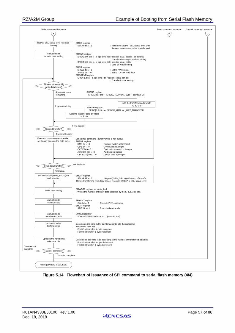
RZ/A2M Group Example of Booting from Serial Flash Memory
R01AN4333EJ0100 Rev.1.00 Page 57 of 86 Dec. 18, 2018
Figure 5.14 Flowchart of issuance of SPI command to serial flash memory (4/4)
QSPIn_SSL signal level retentionsetting
SMCR register SSLKP bit ← 1 : Retain the QSPIn_SSL signal level until
the next access starts after transfer end
Manual modetransfer data setting
SMENR register SPIDE[3:0] bits ← p_spi_cmd_tbl->transfer_data_access_bit_setting
: Transfer data output method setting SPIDB[1:0] bits ← p_spi_cmd_tbl->transfer_data_width
: Data bit width settingSMCR register SPIWE bit ← 1 : Set to "Write data" SPIRE bit ← 0 : Set to "Do not read data"SMDRENR register SPIDRE bit ← p_spi_cmd_tbl->transfer_data_sdr_ddr
: Transfer format setting
Manual modetransfer start
PHYCNT register CAL bit ← 1 : Execute PHY calibrationSMCR register SPIE bit ← 1 : Execute data transfer
Manual modetransfer end wait
Second transfer?
If second or subsequent transfer,set to only execute the data cycle
Set so that command~dummy cycle is not output.SMENR register DME bit ← 0 : Dummy cycles not inserted CDE bit ← 0 : Command not output OCDE bit ← 0 : Optional command not output ADE[3:0] bits ← 0 : Address not output OPDE[3:0] bits ← 0 : Option data not output
Final data transfer?
Set to cancel QSPIn_SSL signal level retention
SMCR register SSLKP bit ← 0 : Negate QSPIn_SSL signal at end of transferBefore transferring final data, cancel retention of QSPIn_SSL signal level
Number of remaining write data bytes?
Sets the transfer data bit widthto 32 bits
4 bytes or more remaining
If second transfer
Transfer complete?
If first transfer
Final data
Transfer not complete
Write command issuance
E
return (SPIBSC_SUCCESS)
F G
Read command issuance Control command issuance
Not final data
SMWDR0 register ← *write_buff Writes the number of bits of data specified by the SPIDE[3:0] bits.
CMNSR register Wait until TEND bit is set to "1 (transfer end)"
SMENR register SPIDE[3:0] bits ← SPIBSC_MANUAL_32BIT_TRANSFER
Write data setting
Transfer complete
1 byte remaining
Sets the transfer data bit widthto 8 bits
SMENR register SPIDE[3:0] bits ← SPIBSC_MANUAL_8BIT_TRANSFER
Increment writebuffer pointer
Increments the write buffer pointer according to the number oftransferred data bits. For 32-bit transfer: 4-byte increment For 8-bit transfer: 1-byte increment
Updates the remaining write data bits
Decrements the write_size according to the number of transferred data bits. For 32-bit transfer: 4-byte decrement For 8-bit transfer: 1-byte decrement

RZ/A2M Group Example of Booting from Serial Flash Memory
R01AN4333EJ0100 Rev.1.00 Page 58 of 86 Dec. 18, 2018
5.10.6 SPIBSC Read Timing Calibration for DDR Transfer When SPIBSC communicates with serial flash memory by DDR transfer, it must need to calibrate data capture delay for valid reading.
Figure 5.15 shows the Allocation of test pattern for calibrate processing. The test pattern is stored in serial flash memory and using for its calibrating operation.
In calibration routine, reads the test pattern by per capture delay that increase gradually, and choose median delay that can read valid pattern. The SPIBSC registers PHYADJ1, PHYADJ2, and PHYCNT.CKSEL are used for applying capture delay.
Figure 5.15 Allocation of test pattern for calibrate processing
Loader program
Not used
Applicationprogram
Not used
RZ/A2M groupAddress space
H'2000_0000
H'2000_8000
H'2001_0000
H'2400_0000
-
H'2FFF_FFFF
g_spibsc_test_pattern SPIBSC_TEST_PATTERN_EXPECTED_VALUE
4-bytes fixed dataAddress of the fixed data

RZ/A2M Group Example of Booting from Serial Flash Memory
R01AN4333EJ0100 Rev.1.00 Page 59 of 86 Dec. 18, 2018
Figure 5.16 to Figure 5.18 shows Flowchart of Timing Calibration for DDR Transfer. This function must use when the SPIBSC configures as manual transfer mode.
Figure 5.16 Flowchart of Timing Calibration for DDR Transfer (1/3)
Complete the read check for timing ajustment setting of 13 step?
incomplete(index < 13)
complete(index ≥ 13)
The read value match the fixed value data stored in the flash
memory?
YES(Match)
NO(Mismatch)
Store NG to the table
Store OK to the table
gs_ok_ng_result[ index ] ← 1 (OK)
Increment index number for table search
Initialize index number for table search
index++
R_SPIBSC_AdjustPhy
Enable access to registers for timing adjustment
A
Get register setting value (zz, xy) from timing adjustment register table
Register setting processingfor timing adjustment
To search the register table for timing adjustment from the beginning, initialize the index. index ← 0
PHYCNT.CKSEL[1:0] ← zzPHYADJ2 register ← H'0000 00xyPHYADJ1 register ← H'8000 0032
gs_ok_ng_result[ index ] ← 0 (NG)
Polls until the CMNSR.TEND bit is set to 1 (transfer end).
The member variables of the timing adjustment register table (gs_spibsc_phy_adj [index]) are as follows. zz : The setting value to PHYCNT.CKSEL[1:0]bit x : The setting value to bit4 of PHYADJ2 register y : The setting value to bit0 of PHYADJ2 register
Changing the data Input timing, check whether it can be read correctly, store the result (OK / NG) in the table
Wait for access to serial flash memory to be completed
Execute the DDR read command, then read the area "&g_spibsc_test_pattern" of the serial flash memory where fixed value data is stored
Execute DDR read command by manual mode
Userdef_SPIBSC_SFLASH_Read
After register setting for timing adjustment, Confirms whether the data was read from the flash memory correctly.
In order to be able to access the timing adjustment register,Execute the following register setting processing. PHYADJ2 register ← H'A539 0000 PHYADJ1 register ← H'8000 0000 PHYADJ2 register ← H'0000 9191 PHYADJ1 register ← H'8000 0022 PHYADJ2 register ← H'0000 9191 PHYADJ1 register ← H'8000 0024
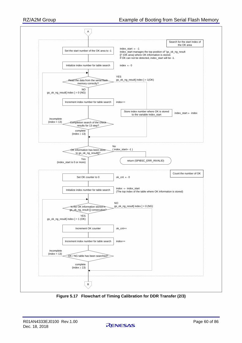
RZ/A2M Group Example of Booting from Serial Flash Memory
R01AN4333EJ0100 Rev.1.00 Page 60 of 86 Dec. 18, 2018
Figure 5.17 Flowchart of Timing Calibration for DDR Transfer (2/3)
A
OK information has been store to gs_ok_ng_result[]?
Yes(index_start is 0 or more) return (SPIBSC_ERR_INVALID)
Completion search of the check results for 13 step?
incomplete(index < 13)
complete(index ≥ 13)
Increment index number for table search
Set the start number of the OK area to -1
Read the data from the serial flash memory correctly?
index++
index_start ← index
index_start ← -1index_start manages the top position of "gs_ok_ng_result []" (OK area) where OK information is stored.If OK can not be detected, index_start will be -1.
Store index number where OK is stored to the variable index_start
Initialize index number for table search index ← 0
OK / NG table has been searched?
incomplete(index < 13)
complete(index ≥ 13)
Increment index number for table search
Set OK counter to 0
Is the OK information stored in gs_ok_ng_result [] consecutive?
YESgs_ok_ng_result[ index ] = 1 (OK)
NOgs_ok_ng_result[ index ] = 0 (NG)
index++
ok_cnt ← 0
Initialize index number for table search index ← index_start (The top index of the table where OK information is stored)
Increment OK counter ok_cnt++
Search for the start Index of the OK area
Count the number of OK
B
NOgs_ok_ng_result[ index ] = 0 (NG)
YESgs_ok_ng_result[ index ] = 1(OK)
No( index_start= -1 )
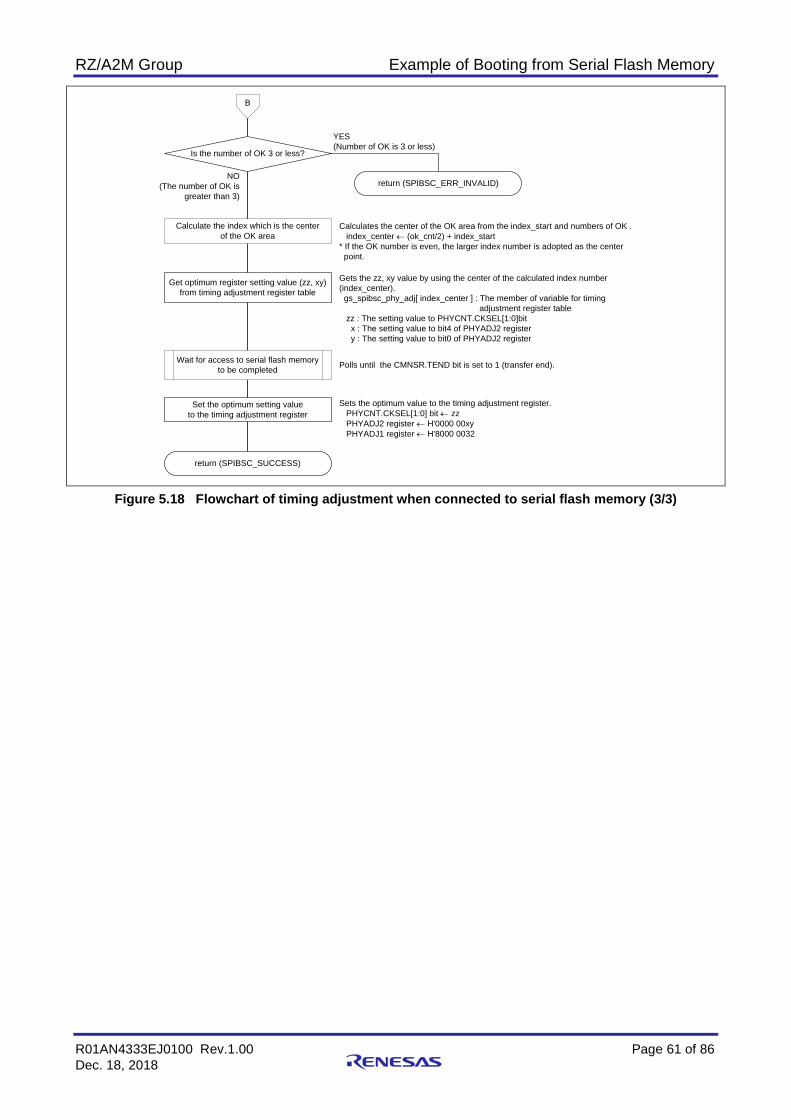
RZ/A2M Group Example of Booting from Serial Flash Memory
R01AN4333EJ0100 Rev.1.00 Page 61 of 86 Dec. 18, 2018
Figure 5.18 Flowchart of timing adjustment when connected to serial flash memory (3/3)
return (SPIBSC_SUCCESS)
Set the optimum setting value to the timing adjustment register
Is the number of OK 3 or less?
YES(Number of OK is 3 or less)
NO(The number of OK is
greater than 3)
Sets the optimum value to the timing adjustment register. PHYCNT.CKSEL[1:0] bit ← zz PHYADJ2 register ← H'0000 00xy PHYADJ1 register ← H'8000 0032
Get optimum register setting value (zz, xy) from timing adjustment register table
return (SPIBSC_ERR_INVALID)
Calculates the center of the OK area from the index_start and numbers of OK . index_center ← (ok_cnt/2) + index_start* If the OK number is even, the larger index number is adopted as the center point.
Calculate the index which is the center of the OK area
B
Wait for access to serial flash memory to be completed Polls until the CMNSR.TEND bit is set to 1 (transfer end).
Gets the zz, xy value by using the center of the calculated index number (index_center). gs_spibsc_phy_adj[ index_center ] : The member of variable for timing adjustment register table zz : The setting value to PHYCNT.CKSEL[1:0]bit x : The setting value to bit4 of PHYADJ2 register y : The setting value to bit0 of PHYADJ2 register

RZ/A2M Group Example of Booting from Serial Flash Memory
R01AN4333EJ0100 Rev.1.00 Page 62 of 86 Dec. 18, 2018
6. Application Example 6.1 Operation of the Sample Code Used in its Initial State The sample code in its initial state accesses the Macronix serial flash memory (product No.: MX25L51245GXD) according to the settings that are summarized in Table 6.1.
Table 6.1 Sample Code Access Settings
Item Setting Serial flash memory • Macronix serial flash memory
• Model name: MX25L51245GXD • Read command used: H'EE (4DTRD4B)
4-bit bus, DDR transfer Number of dummy cycles required: 8 (When running at a maximum operating frequency of 66MHz)
SPIBSC • Number of serial flash memory devices to be connected: 1
• Data bus width: 4 bits • Number of address bytes: 4 bytes
(Number of bytes to be issued when specifying an address)
• Transfer format in read mode: DDR transfer Figure 6.1 shows the Read operation in DDR transfer mode (initial state of the sample code). Table 6.2 shows the Register settings for sample .
In the command cycle, the MX25L51245GXD samples the input data at the rising edge of the clock in SDR transfer mode. The SPIBSC begins data output with respect to the falling edge of the clock and continues data output processing at the rising edge. The MX25L51245GXD samples the MSB of the output data from the SPIBSC at the rising edge of the first QSPIn_SPCLK.
The address cycle and data cycle perform DDR transfer. In the address cycle, the SPIBSC starts address output at the rising edge of the clock after the command cycle has finished, and after that outputs at both the rising and falling edges of the clock. The MX25L51245GXD starts sampling the input of the address cycle at the rising edge, and after that samples at both edges.
The MX25L51245GXD also begins data output at the falling edge of the last clock of the dummy cycle, and after that outputs data at both the rising and falling edges of the clock. The SPIBSC samples the input data at the rising edge of the first clock of the data cycle, and after that samples the input data at both edges.
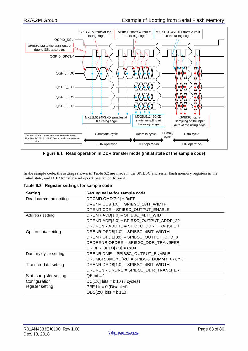
RZ/A2M Group Example of Booting from Serial Flash Memory
R01AN4333EJ0100 Rev.1.00 Page 63 of 86 Dec. 18, 2018
Figure 6.1 Read operation in DDR transfer mode (initial state of the sample code)
In the sample code, the settings shown in Table 6.2 are made in the SPIBSC and serial flash memory registers in the initial state, and DDR transfer read operations are performed.
Table 6.2 Register settings for sample code
Setting Setting value for sample code Read command setting DRCMR.CMD[7:0] = 0xEE
DRENR.CDB[1:0] = SPIBSC_1BIT_WIDTH DRENR.CDE = SPIBSC_OUTPUT_ENABLE
Address setting DRENR.ADB[1:0] = SPIBSC_4BIT_WIDTH DRENR.ADE[3:0] = SPIBSC_OUTPUT_ADDR_32 DRDRENR.ADDRE = SPIBSC_DDR_TRANSFER
Option data setting DRENR.OPDB[1:0] = SPIBSC_4BIT_WIDTH DRENR.OPDE[3:0] = SPIBSC_OUTPUT_OPD_3 DRDRENR.OPDRE = SPIBSC_DDR_TRANSFER DROPR.OPD3[7:0] = 0x00
Dummy cycle setting DRENR.DME = SPIBSC_OUTPUT_ENABLE DRDMCR.DMCYC[4:0] = SPIBSC_DUMMY_07CYC
Transfer data setting DRENR.DRDB[1:0] = SPIBSC_4BIT_WIDTH DRDRENR.DRDRE = SPIBSC_DDR_TRANSFER
Status register setting QE bit = 1 Configuration register setting
DC[1:0] bits = b'10 (8 cycles) PBE bit = 0 (Disabled) ODS[2:0] bits = b'110
QSPI0_SPCLK
QSPI0_SSL
QSPI0_IO0
Command cycle Dummy cycle
Data cycle
QSPI0_IO1
QSPI0_IO2
QSPI0_IO3
SPIBSC starts the MSB output due to SSL assertion.
SPIBSC outputs at the falling edge
MX25L51245GXD starts output at the falling edge
MX25L51245GXD samples atthe rising edge
SPIBSC starts sampling of the input
data at the rising edge
SPIBSC starts output at the falling edge
MX25L51245GXDstarts sampling at
the rising edge
Address cycle
SDR operation DDR operation
Red line: SPIBSC write and read standard clockBlue line: MX25L51245GXD read and write standard
clockDDR operation
RZ/A2M Group Example of Booting from Serial Flash Memory
R01AN4333EJ0100 Rev.1.00 Page 64 of 86 Dec. 18, 2018
The sample code calls the user-defined function Userdef_SPIBSC_SFLASH_SetMode to set up the serial flash memory registers within the R_SC_HardwareSetup function which is executed during initialization, after switching to manual mode with the R_SPIBSC_ChangeMode function. The Userdef_SPIBSC_SFLASH_SetMode function configures the status register and configuration register of the serial flash memory according to the specifications for the read command to be used.
Table 6.3 shows MX25L51245GXD status register and Table 6.4 shows MX25L51245GXD configuration register. The Userdef_SPIBSC_SFLASH_SetMode function is used to set the bites denoted by " " in the tables and other bits are left to hold their initial value.
Table 6.3 MX25L51245GXD status register
Bit position Bit name
Attribute (Note) Description
7 SRWD NV Status register write protect 1 = Status register write disabled 0 = Status register write enabled
6 QE NV Quad enable 1 = Quad enable 0 = Not Quad enable
5,4,3,2 BP3,BP2,BP1,BP0 NV Level of protected block 1 WEL V Write enable latch
1 = Write enable 0 = Not write enable
0 WIP V Write in progress bit 1 = Write operation 0 = Not in write operation
Note: "NV" in the attribute column denotes "Non-volatile bit" and "V" denotes "Volatile bit." Table 6.4 MX25L51245GXD configuration register
Bit position Bit name
Attribute (Note 1) Description
7,6 DC1, DC0 V Dummy cycle 1, Dummy cycle 0 DC[1:0] = B'10 (Note 2)
5 4BYTE V 0 = 3-byte address mode 1 = 4-byte address mode
4 PBE V Preamble bit enable 0 = Disable 1 = Enable
3 TB OTP Top/bottom selected 0 = Top area protect 1 = Bottom area protect
2,1,0 ODS2, ODS1, ODS0
V Output driver strength (ODS2 = 1, ODS1 = 1, ODS0 = 0) (Note 3)
Note: 1. "NV" in the attribute column denotes "Non-volatile bit" and "OTP" denotes "One-time programmable bit". 2. As seen from Table 6.5, the number of dummy cycles differs depending on the read command to
be used. The sample code uses H'EE as the read command and therefore loads DC[1:0] bits with a value of B'10 so that an optimum dummy cycle count can be obtained.
3. The sample code uses the settings ODS2 = 1, ODS1 = 1, and ODS0 = 0 to obtain optimum AC timing characteristics about the data hold time (tCHDX) and data output delay time (tCLQV) of the MX25L51245GXD when connected to the RZ/A2M. (This setting is possible when the load capacity of the device to be connected to the MX25L51245GXD is 15pF or less and 3.0 to 3.6V is applied to the power source (VCC) of the MX25L51245GXD.)
RZ/A2M Group Example of Booting from Serial Flash Memory
R01AN4333EJ0100 Rev.1.00 Page 65 of 86 Dec. 18, 2018
Table 6.5 shows a List of numbers of dummy cycles necessary for the operating frequency of the MX25L51245GXD. The number of necessary dummy cycles differ depending on the read command and operating frequency to be used. Since the sample code uses the H'EE command as the read command and sets QSPIn_SPCLK to 66MHz, its optimum setting is DC[1:0] = B'10 which yields a dummy cycle count of 8 cycles.
When changing the read command to be used, set the number of dummy cycles according to the new read command and the frequency of QSPIn_SPCLK.
Table 6.5 List of numbers of dummy cycles necessary for the operating frequency of the
MX25L51245GXD
Read command Configuration register DC[1:0] bits B'00 B'01 B'10 B'11
FAST READ (H'0B) FAST READ4B (H'0C)
8 cycles /133MHz
6 cycles /133MHz
8 cycles /133MHz
10 cycles /66MHz
FASTDTRD (H'0D) FRDTRD4B H'0E)
8 cycles /66MHz
6 cycles /66MHz
8 cycles /66MHz
10 cycles /83MHz
4READ (H'EB) 4READ4B (H'EC)
6 cycles /84MHz
4 cycles /70MHz (Note 2)
8 cycles /104MHz
10 cycles /133MHz
4DTRD (H'ED) 4DTRD4B (H'EE)
6 cycles /52MHz
4 cycles /42MHz
8 cycles /66MHz (Note 1)
10 cycles /100MHz
Note: 1. In the default state of the sample code, 4DTRD4B (H'EE) is used as the read command in external address space read mode. In the sample code, the DC[1:0] bits are set to B'10 in order to achieve the minimum number of dummy cycles at 66Mhz operation.
2. In the sample code, 4READ4B (H'EC) is used for SDR transfer read access in external address space read mode, and the DC[1:0] bits are set to B'01 in order to achieve the minimum number of dummy cycles at 66Mhz operation.
RZ/A2M Group Example of Booting from Serial Flash Memory
R01AN4333EJ0100 Rev.1.00 Page 66 of 86 Dec. 18, 2018
6.2 Changing the Sample Code When Not Changing the Serial Flash Memory 6.2.1 Changing to SDR Transfer Read Command In the sample code, the SDR transfer read command can be used as a read command in external address space read mode. By disabling the macro definition SPIBSC_PRV_DDR_SETTING defined in hwsetup.c, the SDR transfer read command is used for direct access to the serial flash memory. Table 6.6 shows the Register settings for changing to SDR transfer read command.
Table 6.6 Register settings for changing to SDR transfer read command
Setting Value Read command setting DRCMR.CMD[7:0] = 0xEC
DRENR.CDB[1:0] = SPIBSC_1BIT_WIDTH DRENR.CDE = SPIBSC_OUTPUT_ENABLE
Address setting DRENR.ADB[1:0] = SPIBSC_4BIT_WIDTH DRENR.ADE[3:0] = SPIBSC_OUTPUT_ADDR_32 DRDRENR.ADDRE = SPIBSC_SDR_TRANSFER
Option data setting DRENR.OPDB[1:0] = SPIBSC_4BIT_WIDTH DRENR.OPDE[3:0] = SPIBSC_OUTPUT_OPD_3 DRDRENR.OPDRE = SPIBSC_SDR_TRANSFER DROPR.OPD3[7:0] = 0x00
Dummy cycle setting DRENR.DME = SPIBSC_OUTPUT_ENABLE DRDMCR.DMCYC[4:0] = SPIBSC_DUMMY_02CYC
Transfer data setting DRENR.DRDB[1:0] = SPIBSC_4BIT_WIDTH DRDRENR.DRDRE = SPIBSC_SDR_TRANSFER
Status register setting QE bit = 1 Configuration register setting
DC[1:0] bits = b'01 (4 cycles) PBE bit = 0 (Disabled) ODS[2:0] bits = b'110
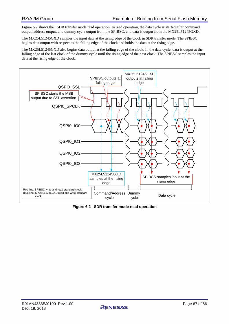
RZ/A2M Group Example of Booting from Serial Flash Memory
R01AN4333EJ0100 Rev.1.00 Page 67 of 86 Dec. 18, 2018
Figure 6.2 shows the SDR transfer mode read operation. In read operation, the data cycle is started after command output, address output, and dummy cycle output from the SPIBSC, and data is output from the MX25L51245GXD.
The MX25L51245GXD samples the input data at the rising edge of the clock in SDR transfer mode. The SPIBSC begins data output with respect to the falling edge of the clock and holds the data at the rising edge.
The MX25L51245GXD also begins data output at the falling edge of the clock. In the data cycle, data is output at the falling edge of the last clock of the dummy cycle until the rising edge of the next clock. The SPIBSC samples the input data at the rising edge of the clock.
Figure 6.2 SDR transfer mode read operation
QSPI0_SPCLK
QSPI0_SSL
QSPI0_IO0
Command/Address cycle
Dummy cycle Data cycle
QSPI0_IO1
QSPI0_IO2
QSPI0_IO3
SPIBSC starts the MSB output due to SSL assertion.
SPIBSC outputs at falling edge
MX25L51245GXD outputs at falling
edge
MX25L51245GXD samples at the rising
edgeSPIBCS samples input at the
rising edge
Red line: SPIBSC write and read standard clockBlue line: MX25L51245GXD read and write standard
clock
RZ/A2M Group Example of Booting from Serial Flash Memory
R01AN4333EJ0100 Rev.1.00 Page 68 of 86 Dec. 18, 2018
6.3 Changing the Sample Code When Changing the Serial Flash Memory When changing the serial flash memory, the sample code should be changed according to the specifications of the serial flash memory to be used.
Table 6.7 lists the Points for changing sample code.
Table 6.7 Points for changing sample code
Change point Description
Related section number
Signal Output when a Read Command is Issued
Change the output signal to be sent to the serial flash memory when a read command is issued in external address space read mode according to the specifications for the serial flash memory read command to be used.
6.3.1
Setting up the Serial Flash Memory Registers
The registers in the serial flash memory required to use the SPIBSC in external address read mode are made according to the serial flash memory to be used.
6.3.2
Serial Flash Memory Write Completion Wait
Wait for the write to the serial flash memory to be completed according to the serial flash memory to be used.
6.3.3
Serial Flash Memory Status Register Read
Read the status registers in the serial flash memory according to the serial flash memory to be used.
6.3.4
Serial Flash Memory Configuration Register Read
Read the configuration registers in the serial flash memory according to the serial flash memory to be used.
6.3.5
Serial Flash Memory Write Enable
The settings for the registers in the serial flash memory are made to enable write operations according to the serial flash memory to be used. (Note)
6.3.6
Serial Flash Memory Status/Configuration Register Write
Write the status/configuration registers in the serial flash memory according to the serial flash memory to be used.
6.3.7
Note: In some cases, it is necessary to enable write operations to the serial flash memory in order to make settings to the registers in the serial flash memory.
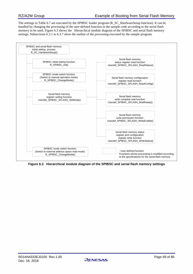
RZ/A2M Group Example of Booting from Serial Flash Memory
R01AN4333EJ0100 Rev.1.00 Page 69 of 86 Dec. 18, 2018
The settings in Table 6.7 are executed by the SPIBSC loader program (R_SC_HardwareSetup function). It can be handled by changing the processing of the user-defined function in the sample code according to the serial flash memory to be used. Figure 6.3 shows the Hierarchical module diagram of the SPIBSC and serial flash memory settings. Subsections 6.3.1 to 6.3.7 show the outline of the processing executed by the sample program.
Figure 6.3 Hierarchical module diagram of the SPIBSC and serial flash memory settings
SPIBSC and serial flash memoryinitial setting process
R_SC_HardwareSetup()
SPIBSC initial setting functionR_SPIBSC_Init()
SPIBSC mode switch function(Switch to manual operation mode)
R_SPIBSC_ChangeMode()
Serial flash memoryregister setting function
Userdef_SPIBSC_SFLASH_SetMode()
: User-defined functionFunctions whose processing is modified according to the specifications for the serial flash memory
SPIBSC mode switch function(Switch to external address space read mode)
R_SPIBSC_ChangeMode()
Serial flash memorywrite complete wait function
Userdef_SPIBSC_SFLASH_WaitReady()
Serial flash memorystatus register read function
Userdef_SPIBSC_SFLASH_ReadStatus()
Serial flash memory configurationregister read function
Userdef_SPIBSC_SFLASH_ReadConfig()
Serial flash memorywrite permission function
Userdef_SPIBSC_SFLASH_WriteEnable()
Serial flash memory statusregister and configuration
register write functionUserdef_SPIBSC_SFLASH_WriteStatus()
RZ/A2M Group Example of Booting from Serial Flash Memory
R01AN4333EJ0100 Rev.1.00 Page 70 of 86 Dec. 18, 2018
6.3.1 Signal Output when a Read Command is Issued In external address space read mode, a read access to the SPI multi-I/O bus space is initiated by sending a signal, which is converted for SPI communication, to the serial flash memory when issuing the read command. In the case of changing the serial flash memory to be used, the output signal for issuing a read command needs to be changed according to the specifications for the serial flash memory read command.
The SPIBSC allows the read command signal to be output to the serial flash memory by setting up the SPIBSC register in the external address space read mode.
In the sample code, the SPIBSC register settings can be changed and the output signal when a read command is issued can be changed by changing the contents of the SPIBSC external address space read mode's read command settings tables (Table 6.8, Table 6.9). The SPIBSC register settings specified in the read command settings tables are made by executing the SPIBSC operating mode setting function (R_SPIBSC_ChangeMode). The serial flash memory register settings related to the read command settings (number of dummy cycles, bit width, etc.) are made by executing the serial flash memory register setting function (Userdef_SPIBSC_SFLASH_SetMode). Even if executing register settings in the serial flash memory with the Userdef_SPIBSC_SFLASH_SetMode function, make the changes according to the specifications of the serial flash memory to be used.
Figure 6.4 shows the Correspondence between SPIBSC register settings and waveforms output to serial flash memory during external address read operation. Refer to these example settings when changing the settings in the external address space read mode's read command settings tables (Table 6.8 and Table 6.9) to match the read command of the serial flash memory used.
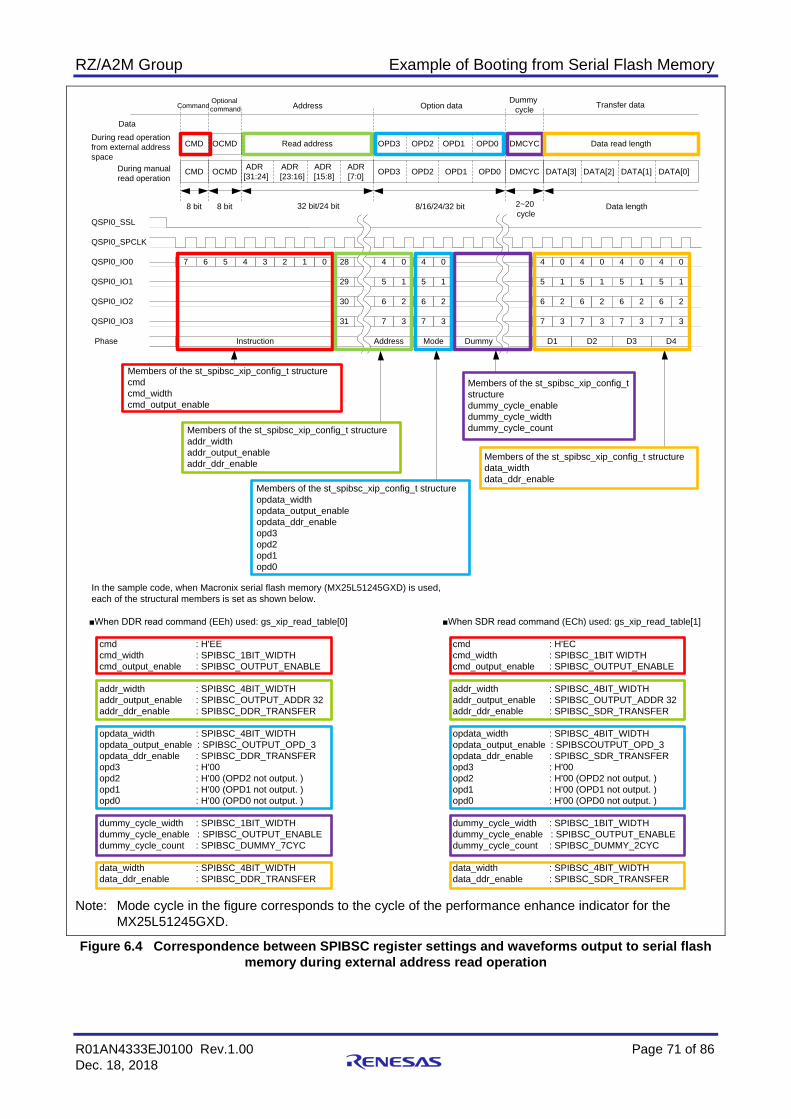
RZ/A2M Group Example of Booting from Serial Flash Memory
R01AN4333EJ0100 Rev.1.00 Page 71 of 86 Dec. 18, 2018
Note: Mode cycle in the figure corresponds to the cycle of the performance enhance indicator for the
MX25L51245GXD.
Figure 6.4 Correspondence between SPIBSC register settings and waveforms output to serial flash memory during external address read operation
■When DDR read command (EEh) used: gs_xip_read_table[0]
cmd : H'EE cmd_width : SPIBSC_1BIT_WIDTH cmd_output_enable : SPIBSC_OUTPUT_ENABLE
addr_width : SPIBSC_4BIT_WIDTH addr_output_enable : SPIBSC_OUTPUT_ADDR 32 addr_ddr_enable : SPIBSC_DDR_TRANSFER
opdata_width : SPIBSC_4BIT_WIDTH opdata_output_enable : SPIBSC_OUTPUT_OPD_3 opdata_ddr_enable : SPIBSC_DDR_TRANSFER opd3 : H'00 opd2 : H'00 (OPD2 not output. ) opd1 : H'00 (OPD1 not output. ) opd0 : H'00 (OPD0 not output. )
dummy_cycle_width : SPIBSC_1BIT_WIDTH dummy_cycle_enable : SPIBSC_OUTPUT_ENABLE dummy_cycle_count : SPIBSC_DUMMY_7CYC
data_width : SPIBSC_4BIT_WIDTH data_ddr_enable : SPIBSC_DDR_TRANSFER
■When SDR read command (ECh) used: gs_xip_read_table[1]
cmd : H'EC cmd_width : SPIBSC_1BIT WIDTH cmd_output_enable : SPIBSC_OUTPUT_ENABLE
addr_width : SPIBSC_4BIT_WIDTH addr_output_enable : SPIBSC_OUTPUT_ADDR 32 addr_ddr_enable : SPIBSC_SDR_TRANSFER
opdata_width : SPIBSC_4BIT_WIDTH opdata_output_enable : SPIBSCOUTPUT_OPD_3 opdata_ddr_enable : SPIBSC_SDR_TRANSFER opd3 : H'00 opd2 : H'00 (OPD2 not output. ) opd1 : H'00 (OPD1 not output. ) opd0 : H'00 (OPD0 not output. )
dummy_cycle_width : SPIBSC_1BIT_WIDTH dummy_cycle_enable : SPIBSC_OUTPUT_ENABLE dummy_cycle_count : SPIBSC_DUMMY_2CYC
data_width : SPIBSC_4BIT_WIDTH data_ddr_enable : SPIBSC_SDR_TRANSFER
In the sample code, when Macronix serial flash memory (MX25L51245GXD) is used,each of the structural members is set as shown below.
CMD OCMD Read address DMCYC Data read length
Transfer dataDummycycleOption dataAddressOptional
commandCommand
CMD OCMD ADR ADR ADR ADR[31:24] [23:16] [15:8] [7:0] DMCYC
DataDuring read operation from external address space
During manual read operation
OPD3 OPD2 OPD1 OPD0
OPD3 OPD2 OPD1 OPD0
DATA[3] DATA[2] DATA[1] DATA[0]
8 bit 8 bit 8/16/24/32 bit 2~20cycle
Data length32 bit/24 bit
Members of the st_spibsc_xip_config_t structurecmdcmd_widthcmd_output_enable
Members of the st_spibsc_xip_config_t structureaddr_widthaddr_output_enableaddr_ddr_enable
Members of the st_spibsc_xip_config_t structuredummy_cycle_enabledummy_cycle_widthdummy_cycle_count
Members of the st_spibsc_xip_config_t structuredata_widthdata_ddr_enable
Members of the st_spibsc_xip_config_t structureopdata_widthopdata_output_enableopdata_ddr_enableopd3opd2opd1opd0
QSPI0_SSL
QSPI0_SPCLK
QSPI0_IO0
QSPI0_IO1
QSPI0_IO2
QSPI0_IO3
Phase
7
Instruction
6 5 4 3 2 1 0 4
5
6
7
0
1
2
3
28
29
30
31
Address Mode Dummy D1 D2 D3 D4
4
5
6
7
0
1
2
3
4
5
6
7
0
1
2
3
4
5
6
7
0
1
2
3
4
5
6
7
0
1
2
3
4
5
6
7
0
1
2
3
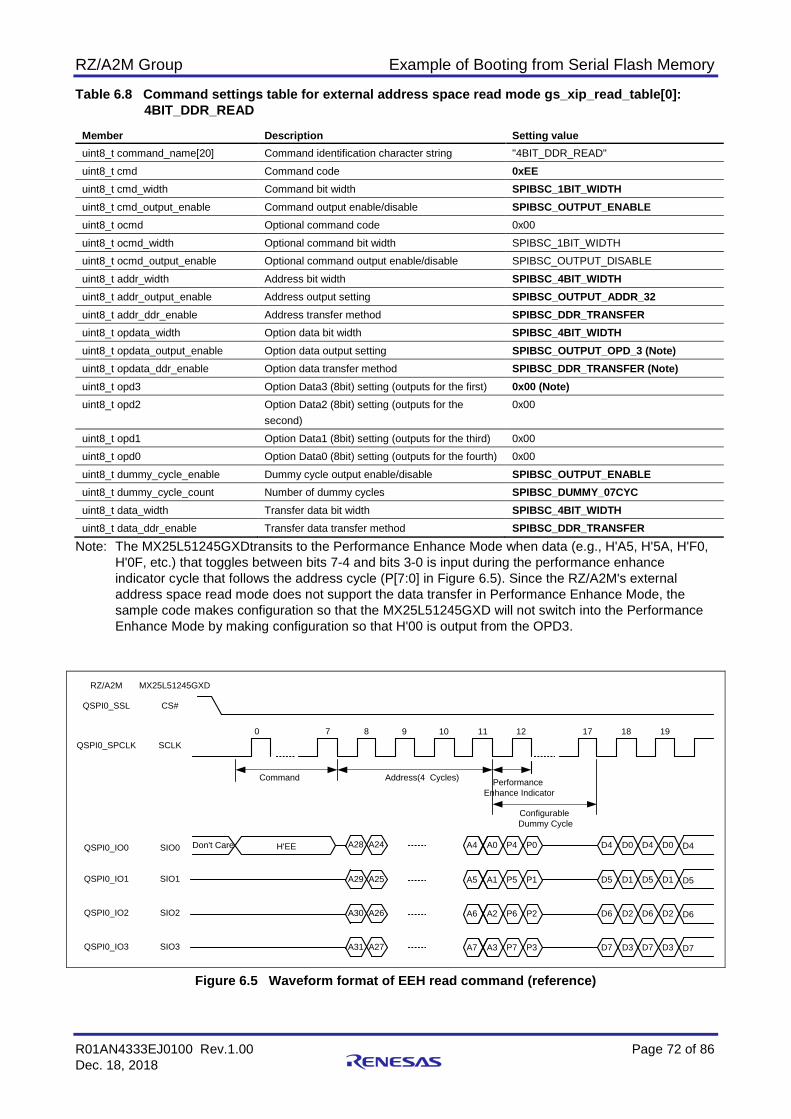
RZ/A2M Group Example of Booting from Serial Flash Memory
R01AN4333EJ0100 Rev.1.00 Page 72 of 86 Dec. 18, 2018
Table 6.8 Command settings table for external address space read mode gs_xip_read_table[0]: 4BIT_DDR_READ
Member Description Setting value uint8_t command_name[20] Command identification character string "4BIT_DDR_READ" uint8_t cmd Command code 0xEE uint8_t cmd_width Command bit width SPIBSC_1BIT_WIDTH uint8_t cmd_output_enable Command output enable/disable SPIBSC_OUTPUT_ENABLE uint8_t ocmd Optional command code 0x00 uint8_t ocmd_width Optional command bit width SPIBSC_1BIT_WIDTH uint8_t ocmd_output_enable Optional command output enable/disable SPIBSC_OUTPUT_DISABLE uint8_t addr_width Address bit width SPIBSC_4BIT_WIDTH uint8_t addr_output_enable Address output setting SPIBSC_OUTPUT_ADDR_32 uint8_t addr_ddr_enable Address transfer method SPIBSC_DDR_TRANSFER uint8_t opdata_width Option data bit width SPIBSC_4BIT_WIDTH uint8_t opdata_output_enable Option data output setting SPIBSC_OUTPUT_OPD_3 (Note) uint8_t opdata_ddr_enable Option data transfer method SPIBSC_DDR_TRANSFER (Note) uint8_t opd3 Option Data3 (8bit) setting (outputs for the first) 0x00 (Note) uint8_t opd2 Option Data2 (8bit) setting (outputs for the
second) 0x00
uint8_t opd1 Option Data1 (8bit) setting (outputs for the third) 0x00 uint8_t opd0 Option Data0 (8bit) setting (outputs for the fourth) 0x00 uint8_t dummy_cycle_enable Dummy cycle output enable/disable SPIBSC_OUTPUT_ENABLE uint8_t dummy_cycle_count Number of dummy cycles SPIBSC_DUMMY_07CYC uint8_t data_width Transfer data bit width SPIBSC_4BIT_WIDTH uint8_t data_ddr_enable Transfer data transfer method SPIBSC_DDR_TRANSFER
Note: The MX25L51245GXDtransits to the Performance Enhance Mode when data (e.g., H'A5, H'5A, H'F0, H'0F, etc.) that toggles between bits 7-4 and bits 3-0 is input during the performance enhance indicator cycle that follows the address cycle (P[7:0] in Figure 6.5). Since the RZ/A2M's external address space read mode does not support the data transfer in Performance Enhance Mode, the sample code makes configuration so that the MX25L51245GXD will not switch into the Performance Enhance Mode by making configuration so that H'00 is output from the OPD3.
Figure 6.5 Waveform format of EEH read command (reference)
CS#
SCLK
Command Address(4 Cycles)
0 7 8 9 1110 12 17 18 19
RZ/A2M MX25L51245GXD
QSPI0_SSL
QSPI0_SPCLK
PerformanceEnhance Indicator
ConfigurableDummy Cycle
SIO1QSPI0_IO1 A5 A1 P5 P1A29 A25 D5 D1 D5 D1 D5
SIO2QSPI0_IO2 A6 A2 P6 P2A30 A26 D6 D2 D6 D2 D6
SIO3QSPI0_IO3 A7 A3 P7 P3A31 A27 D7 D3 D7 D3 D7
SIO0 H'EEQSPI0_IO0 A4 A0 P4 P0A28 A24 D4 D0 D4 D0 D4Don't Care
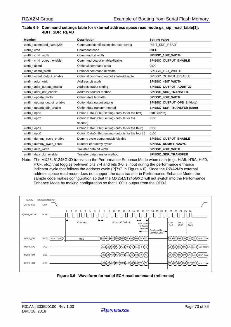
RZ/A2M Group Example of Booting from Serial Flash Memory
R01AN4333EJ0100 Rev.1.00 Page 73 of 86 Dec. 18, 2018
Table 6.9 Command settings table for external address space read mode gs_xip_read_table[1]: 4BIT_SDR_READ
Member Description Setting value uint8_t command_name[20] Command identification character string "4BIT_SDR_READ" uint8_t cmd Command code 0xEC uint8_t cmd_width Command bit width SPIBSC_1BIT_WIDTH uint8_t cmd_output_enable Command output enable/disable SPIBSC_OUTPUT_ENABLE uint8_t ocmd Optional command code 0x00 uint8_t ocmd_width Optional command bit width SPIBSC_1BIT_WIDTH uint8_t ocmd_output_enable Optional command output enable/disable SPIBSC_OUTPUT_DISABLE uint8_t addr_width Address bit width SPIBSC_4BIT_WIDTH uint8_t addr_output_enable Address output setting SPIBSC_OUTPUT_ADDR_32 uint8_t addr_ddr_enable Address transfer method SPIBSC_SDR_TRANSFER uint8_t opdata_width Option data bit width SPIBSC_4BIT_WIDTH uint8_t opdata_output_enable Option data output setting SPIBSC_OUTPUT_OPD_3 (Note) uint8_t opdata_ddr_enable Option data transfer method SPIBSC_SDR_TRANSFER (Note) uint8_t opd3 Option Data3 (8bit) setting (outputs for the first) 0x00 (Note) uint8_t opd2 Option Data2 (8bit) setting (outputs for the
second) 0x00
uint8_t opd1 Option Data1 (8bit) setting (outputs for the third) 0x00 uint8_t opd0 Option Data0 (8bit) setting (outputs for the fourth) 0x00 uint8_t dummy_cycle_enable Dummy cycle output enable/disable SPIBSC_OUTPUT_ENABLE uint8_t dummy_cycle_count Number of dummy cycles SPIBSC_DUMMY_02CYC uint8_t data_width Transfer data bit width SPIBSC_4BIT_WIDTH uint8_t data_ddr_enable Transfer data transfer method SPIBSC_SDR_TRANSFER
Note: The MX25L51245GXD transits to the Performance Enhance Mode when data (e.g., H'A5, H'5A, H'F0, H'0F, etc.) that toggles between bits 7-4 and bits 3-0 is input during the performance enhance indicator cycle that follows the address cycle (P[7:0] in Figure 6.6). Since the RZ/A2M's external address space read mode does not support the data transfer in Performance Enhance Mode, the sample code makes configuration so that the MX25L51245GXD will not switch into the Performance Enhance Mode by making configuration so that H'00 is output from the OPD3.
Figure 6.6 Waveform format of ECH read command (reference)
CS#
SCLK
Command Address(8 Cycles)
0 7 8 9 10
RZ/A2M MX25L51245GXD
QSPI0_SSL
QSPI0_SPCLK
PerformanceEnhanceIndicator
ConfigurableDummy Cycle
SIO1QSPI0_IO1
SIO2QSPI0_IO2
SIO3QSPI0_IO3
SIO0QSPI0_IO0
1 2 3 4 5 6 17 18 19 2011 12 13 14 15 16 22 23 24 25 2621
DataOut1
DataOut2
DataOut3
A4 A0 P4 P0A28 A24 D4 D0 D4 D0A20 A16 A12 A8 D4 D0
A5 A1 P5 P1A29 A25 D5 D1 D5 D1A21 A17 A13 A9 D5 D1
A6 A2 P6 P2A30 A26 D6 D2 D6 D2A22 A18 A14 A10 D6 D2
A7 A3 P7 P3A31 A27 D7 D3 D7 D3A23 A19 A15 A11 D7 D3
H'ECDon't Care Don't Care
Don't Care
Don't Care
Don't Care

RZ/A2M Group Example of Booting from Serial Flash Memory
R01AN4333EJ0100 Rev.1.00 Page 74 of 86 Dec. 18, 2018
6.3.2 Setting up the Serial Flash Memory Registers In the sample code, the user-defined function Userdef_SPIBSC_SFLASH_SetMode executes the processing for the serial flash memory MX25L51245GXD register settings (QE bit of the status register, and DC[1:0] bits, PBE bit, and ODS[2:0] bits of the configuration register) according to the specifications of the read command to be used.
In the sample code, because the Quad read command (H'EE or H'EC) is used as the read command, the status register QE (Quad Enable) bit is set to 1 so the bit width is 4 bits. Also, the DC[1:0] bits of the configuration register are set so that the number of inserted dummy cycles is the minimum needed for the read command and operating frequency used (refer to Table 6.5 List of numbers of dummy cycles necessary for the operating frequency of the MX25L51245GXD for details). Further, the ODS[2:0] bits of the configuration register are set to B'110 to achieve the data output delay (tCLQV) needed for the connection of the RZ/A2M and MX25L51245GXD. Change the execution of the Userdef_SPIBSC_SFLASH_SetMode function so that the serial flash memory's control register setting conforms to the read command specifications of the serial flash memory to be used.
Figure 6.7 shows the Userdef_SPIBSC_SFLASH_SetMode function processing flow of the sample code.
Note: The serial flash memory access is changed from 1-bit width to 4-bit width, and the Status Register
and Configuration Register are set to achieve the minimum number of dummy cycles for the read command. These register settings require the WRSR command to be issued to the serial flash memory after switching the SPIBSC from external address space read mode to manual mode.
Figure 6.7 Userdef_SPIBSC_SFLASH_SetMode function processing flow
Userdef_SPIBSC_SFLASH_SetMode
return
Read Status Register (RDSR[H'05])command issued
Userdef_SPIBSC_SFLASH_ReadStatus()
Read Configuration Register (RDCR[H'15])command issued
Userdef_SPIBSC_SFLASH_ReadConfig()
Write Status Registers (WRSR[H'01])command issued
Userdef_SPIBSC_SFLASH_WriteStatus()
Generate the Status Register setting value
The Read Status Register(RDSR[H'05]) command is issued for the serial flash memory, and the contents read out from the Status Register is stored in the local variable "status".
The Read Configuration Register(RDCR[H'15]) command is issued for the serial flash memory, and the contents read out from Configuration Register is stored in the local variable "config".
The Status Register value stored in the local variable status is used to generate the value to set the QE bit to "1", and then stored in status.Status Register SRWD bit ← 0 : status register write enabled QE bit ← 1 : Quad Enable
Generate the Configuration Register setting valueThe Configuration Register value stored in the local variable config is used to generate the values used to set DC[1:0] bits, PBE bit and ODS[2:0] bits to the following contents, and stored in config.Configuration Register DC[1:0] bits ← B'10 : Number of dummy cycles set to 8 cycles PBE bit ← 0 : Preamble bit disable ODS[2:0] bits ← B'110 : Sets the AC timing characteristics for the data output delay period (tCLQV) to the most appropriate value
The local varialbe status and config values are used to issue the Write Status Register(WRSR[H'01]) command for the serial flash memory, and to overwrite the Status Register and Configuration Register values.

RZ/A2M Group Example of Booting from Serial Flash Memory
R01AN4333EJ0100 Rev.1.00 Page 75 of 86 Dec. 18, 2018
6.3.3 Serial Flash Memory Write Completion Wait The serial flash memory transits to a busy state when the serial flash memory registers (Status Register and Configuration Register) or memory are written to. It is then necessary to wait until the written data is reflected before accessing the serial flash memory.
In the sample code, this wait processing is executed with the Userdef_SPIBSC_SFLASH_WaitReady function.
Implement the Userdef_SPIBSC_SFLASH_WaitReady function according to the specifications of the serial flash memory to be used so that it can wait until completion of serial flash memory writing.
In the sample code, The Status Register WIP bit is read, and wait processing is performed until writing is complete.
Figure 6.8 shows the Userdef_SPIBSC_SFLASH_WaitReady function processing flow of the sample code.
Figure 6.8 Userdef_SPIBSC_SFLASH_WaitReady function processing flow
Userdef_SPIBSC_SFLASH_WaitReady
return
The Read Status Register(RDSR[H'05]) command is issued for the serial flash memory.
Read Status Register (RDSR[H'05])command issued
Userdef_SPIBSC_SFLASH_ReadStatus()
Checks the Status RegisterCheck WIP bit value
write operation
not in write operation
The Status Register WIP(Write in progress) bit is checked,and the Read Status Register command issuing process continues until that value becomes "0".
1 : write operation0 : not in write operation
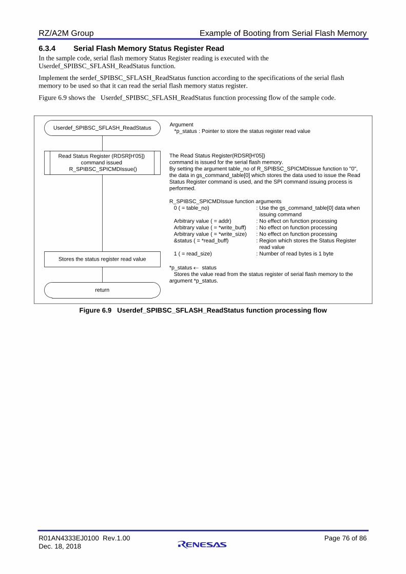
RZ/A2M Group Example of Booting from Serial Flash Memory
R01AN4333EJ0100 Rev.1.00 Page 76 of 86 Dec. 18, 2018
6.3.4 Serial Flash Memory Status Register Read In the sample code, serial flash memory Status Register reading is executed with the Userdef_SPIBSC_SFLASH_ReadStatus function.
Implement the serdef_SPIBSC_SFLASH_ReadStatus function according to the specifications of the serial flash memory to be used so that it can read the serial flash memory status register.
Figure 6.9 shows the Userdef_SPIBSC_SFLASH_ReadStatus function processing flow of the sample code.
Figure 6.9 Userdef_SPIBSC_SFLASH_ReadStatus function processing flow
Userdef_SPIBSC_SFLASH_ReadStatus
return
The Read Status Register(RDSR[H'05])command is issued for the serial flash memory.By setting the argument table_no of R_SPIBSC_SPICMDIssue function to "0",the data in gs_command_table[0] which stores the data used to issue the Read Status Register command is used, and the SPI command issuing process is performed.
R_SPIBSC_SPICMDIssue function arguments 0 ( = table_no) : Use the gs_command_table[0] data when
issuing command Arbitrary value ( = addr) : No effect on function processing Arbitrary value ( = *write_buff) : No effect on function processing Arbitrary value ( = *write_size) : No effect on function processing &status ( = *read_buff) : Region which stores the Status Register read value 1 ( = read_size) : Number of read bytes is 1 byte
Argument *p_status : Pointer to store the status register read value
Read Status Register (RDSR[H'05])command issued
R_SPIBSC_SPICMDIssue()
Stores the status register read value*p_status ← status Stores the value read from the status register of serial flash memory to the argument *p_status.
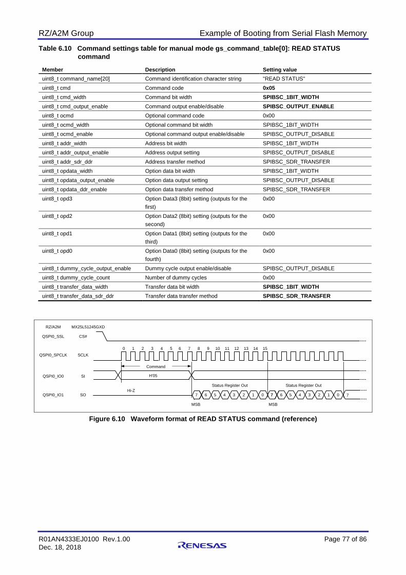
RZ/A2M Group Example of Booting from Serial Flash Memory
R01AN4333EJ0100 Rev.1.00 Page 77 of 86 Dec. 18, 2018
Table 6.10 Command settings table for manual mode gs_command_table[0]: READ STATUS command
Member Description Setting value uint8_t command_name[20] Command identification character string "READ STATUS" uint8_t cmd Command code 0x05 uint8_t cmd_width Command bit width SPIBSC_1BIT_WIDTH uint8_t cmd_output_enable Command output enable/disable SPIBSC_OUTPUT_ENABLE uint8_t ocmd Optional command code 0x00 uint8_t ocmd_width Optional command bit width SPIBSC_1BIT_WIDTH uint8_t ocmd_enable Optional command output enable/disable SPIBSC_OUTPUT_DISABLE uint8_t addr_width Address bit width SPIBSC_1BIT_WIDTH uint8_t addr_output_enable Address output setting SPIBSC_OUTPUT_DISABLE uint8_t addr_sdr_ddr Address transfer method SPIBSC_SDR_TRANSFER uint8_t opdata_width Option data bit width SPIBSC_1BIT_WIDTH uint8_t opdata_output_enable Option data output setting SPIBSC_OUTPUT_DISABLE uint8_t opdata_ddr_enable Option data transfer method SPIBSC_SDR_TRANSFER uint8_t opd3 Option Data3 (8bit) setting (outputs for the
first) 0x00
uint8_t opd2 Option Data2 (8bit) setting (outputs for the second)
0x00
uint8_t opd1 Option Data1 (8bit) setting (outputs for the third)
0x00
uint8_t opd0 Option Data0 (8bit) setting (outputs for the fourth)
0x00
uint8_t dummy_cycle_output_enable Dummy cycle output enable/disable SPIBSC_OUTPUT_DISABLE uint8_t dummy_cycle_count Number of dummy cycles 0x00 uint8_t transfer_data_width Transfer data bit width SPIBSC_1BIT_WIDTH uint8_t transfer_data_sdr_ddr Transfer data transfer method SPIBSC_SDR_TRANSFER
Figure 6.10 Waveform format of READ STATUS command (reference)
7 6 5 4 3 2 1 0 77 6 5 4 3 2 1 0
CS#
SI
SO
SCLK
Hi-Z
H'05
Command
Status Register Out Status Register Out
MSB MSB
0 1 2 3 54 6 7 8 9 1110 12 13 14 15
7
RZ/A2M MX25L51245GXD
QSPI0_SSL
QSPI0_IO0
QSPI0_IO1
QSPI0_SPCLK
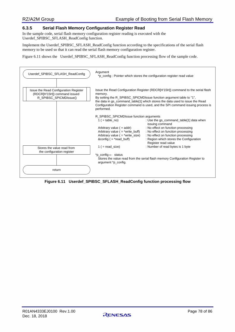
RZ/A2M Group Example of Booting from Serial Flash Memory
R01AN4333EJ0100 Rev.1.00 Page 78 of 86 Dec. 18, 2018
6.3.5 Serial Flash Memory Configuration Register Read In the sample code, serial flash memory configuration register reading is executed with the Userdef_SPIBSC_SFLASH_ReadConfig function.
Implement the Userdef_SPIBSC_SFLASH_ReadConfig function according to the specifications of the serial flash memory to be used so that it can read the serial flash memory configuration register.
Figure 6.11 shows the Userdef_SPIBSC_SFLASH_ReadConfig function processing flow of the sample code.
Figure 6.11 Userdef_SPIBSC_SFLASH_ReadConfig function processing flow
Userdef_SPIBSC_SFLASH_ReadConfig
return
Issue the Read Configuration Register (RDCR[H'15H]) command issued
R_SPIBSC_SPICMDIssue()
Argument *p_config : Pointer which stores the configuration register read value
Issue the Read Configuration Register (RDCR[H'15H]) command to the serial flash memory.By setting the R_SPIBSC_SPICMDIssue function argument table to "1",the data in gs_command_table[1] which stores the data used to issue the Read Configuration Register command is used, and the SPI command issuing process is performed.
R_SPIBSC_SPICMDIssue function arguments 1 ( = table_no) : Use the gs_command_table[1] data when
issuing command Arbitrary value ( = addr) : No effect on function processing Arbitrary value ( = *write_buff) : No effect on function processing Arbitrary value ( = *write_size) : No effect on function processing &config ( = *read_buff) : Region which stores the Configuration
Register read value 1 ( = read_size) : Number of read bytes is 1 byteStores the value read from
the configuration register*p_config ← status Stores the value read from the serial flash memory Configuration Register to argument *p_config.
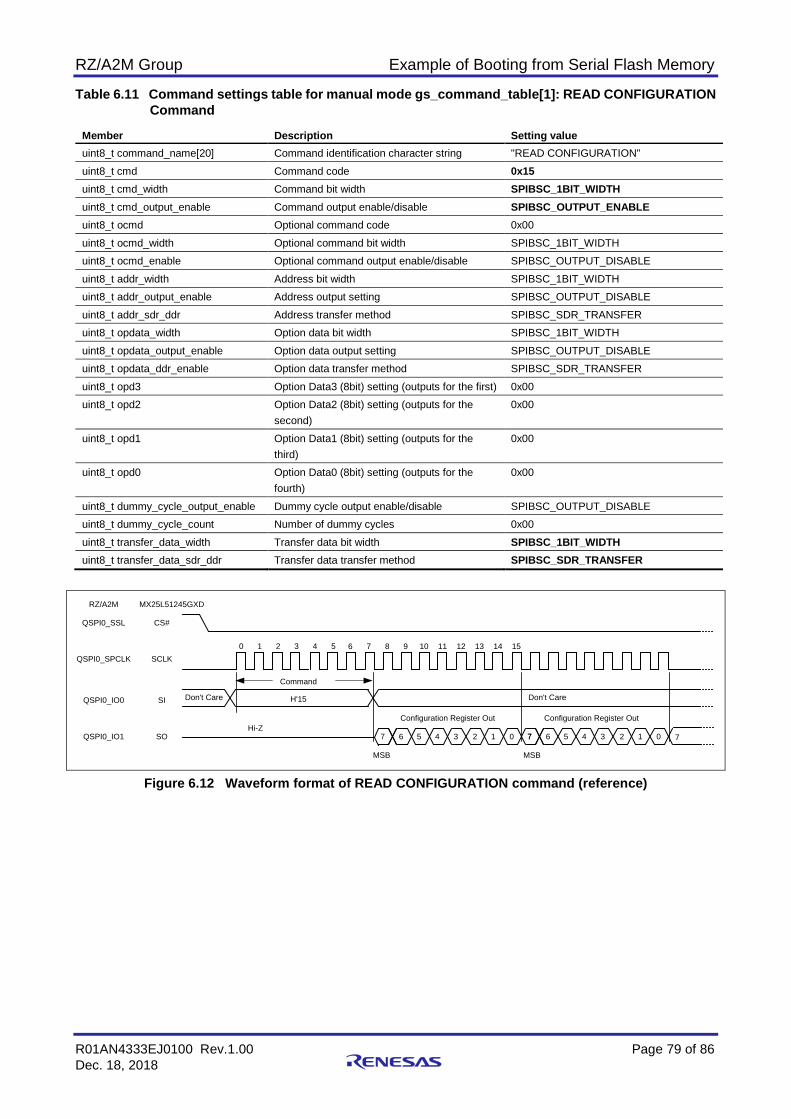
RZ/A2M Group Example of Booting from Serial Flash Memory
R01AN4333EJ0100 Rev.1.00 Page 79 of 86 Dec. 18, 2018
Table 6.11 Command settings table for manual mode gs_command_table[1]: READ CONFIGURATION Command
Member Description Setting value uint8_t command_name[20] Command identification character string "READ CONFIGURATION" uint8_t cmd Command code 0x15 uint8_t cmd_width Command bit width SPIBSC_1BIT_WIDTH uint8_t cmd_output_enable Command output enable/disable SPIBSC_OUTPUT_ENABLE uint8_t ocmd Optional command code 0x00 uint8_t ocmd_width Optional command bit width SPIBSC_1BIT_WIDTH uint8_t ocmd_enable Optional command output enable/disable SPIBSC_OUTPUT_DISABLE uint8_t addr_width Address bit width SPIBSC_1BIT_WIDTH uint8_t addr_output_enable Address output setting SPIBSC_OUTPUT_DISABLE uint8_t addr_sdr_ddr Address transfer method SPIBSC_SDR_TRANSFER uint8_t opdata_width Option data bit width SPIBSC_1BIT_WIDTH uint8_t opdata_output_enable Option data output setting SPIBSC_OUTPUT_DISABLE uint8_t opdata_ddr_enable Option data transfer method SPIBSC_SDR_TRANSFER uint8_t opd3 Option Data3 (8bit) setting (outputs for the first) 0x00 uint8_t opd2 Option Data2 (8bit) setting (outputs for the
second) 0x00
uint8_t opd1 Option Data1 (8bit) setting (outputs for the third)
0x00
uint8_t opd0 Option Data0 (8bit) setting (outputs for the fourth)
0x00
uint8_t dummy_cycle_output_enable Dummy cycle output enable/disable SPIBSC_OUTPUT_DISABLE uint8_t dummy_cycle_count Number of dummy cycles 0x00 uint8_t transfer_data_width Transfer data bit width SPIBSC_1BIT_WIDTH uint8_t transfer_data_sdr_ddr Transfer data transfer method SPIBSC_SDR_TRANSFER
Figure 6.12 Waveform format of READ CONFIGURATION command (reference)
7 6 5 4 3 2 1 0 77 6 5 4 3 2 1 0
CS#
SI
SO
SCLK
Hi-Z
H'15
Command
Configuration Register Out Configuration Register Out
MSB MSB
0 1 2 3 54 6 7 8 9 1110 12 13 14 15
7
RZ/A2M MX25L51245GXD
QSPI0_SSL
QSPI0_IO0
QSPI0_IO1
QSPI0_SPCLK
Don't CareDon't Care
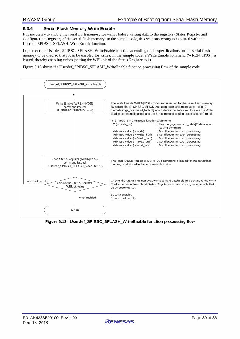
RZ/A2M Group Example of Booting from Serial Flash Memory
R01AN4333EJ0100 Rev.1.00 Page 80 of 86 Dec. 18, 2018
6.3.6 Serial Flash Memory Write Enable It is necessary to enable the serial flash memory for writes before writing data to the registers (Status Register and Configuration Register) of the serial flash memory. In the sample code, this wait processing is executed with the Userdef_SPIBSC_SFLASH_WriteEnable function.
Implement the Userdef_SPIBSC_SFLASH_WriteEnable function according to the specifications for the serial flash memory to be used so that it can be enabled for writes. In the sample code, a Write Enable command (WREN [H'06]) is issued, thereby enabling writes (setting the WEL bit of the Status Register to 1).
Figure 6.13 shows the Userdef_SPIBSC_SFLASH_WriteEnable function processing flow of the sample code.
Figure 6.13 Userdef_SPIBSC_SFLASH_WriteEnable function processing flow
Userdef_SPIBSC_SFLASH_WriteEnable
return
Checks the Status RegisterWEL bit value
Read Status Register (RDSR[H'05])command issued
Userdef_SPIBSC_SFLASH_ReadStatus()
Write Enable (WREN [H'06])command issued
R_SPIBSC_SPICMDIssue()
Checks the Status Register WEL(Write Enable Latch) bit, and continues the Write Enable command and Read Status Register command issuing process until that value becomes "1".
1 : write enabled0 : write not enabled
The Read Status Register(RDSR[H'05]) command is issued for the serial flash memory, and stored in the local variable status.
The Write Enable(WREN[H'06]) command is issued for the serial flash memory.By setting the R_SPIBSC_SPICMDIssue function argument table_no to "2",the data in gs_command_table[2] which stores the data used to issue the Write Enable command is used, and the SPI command issuing process is performed.
R_SPIBSC_SPICMDIssue function arguments 2 ( = table_no) : Use the gs_command_table[2] data when
issuing command Arbitrary value ( = addr) : No effect on function processing Arbitrary value ( = *write_buff) : No effect on function processing Arbitrary value ( = *write_size) : No effect on function processing Arbitrary value ( = *read_buff) : No effect on function processing Arbitrary value ( = read_size) : No effect on function processing
write not enabled
write enabled
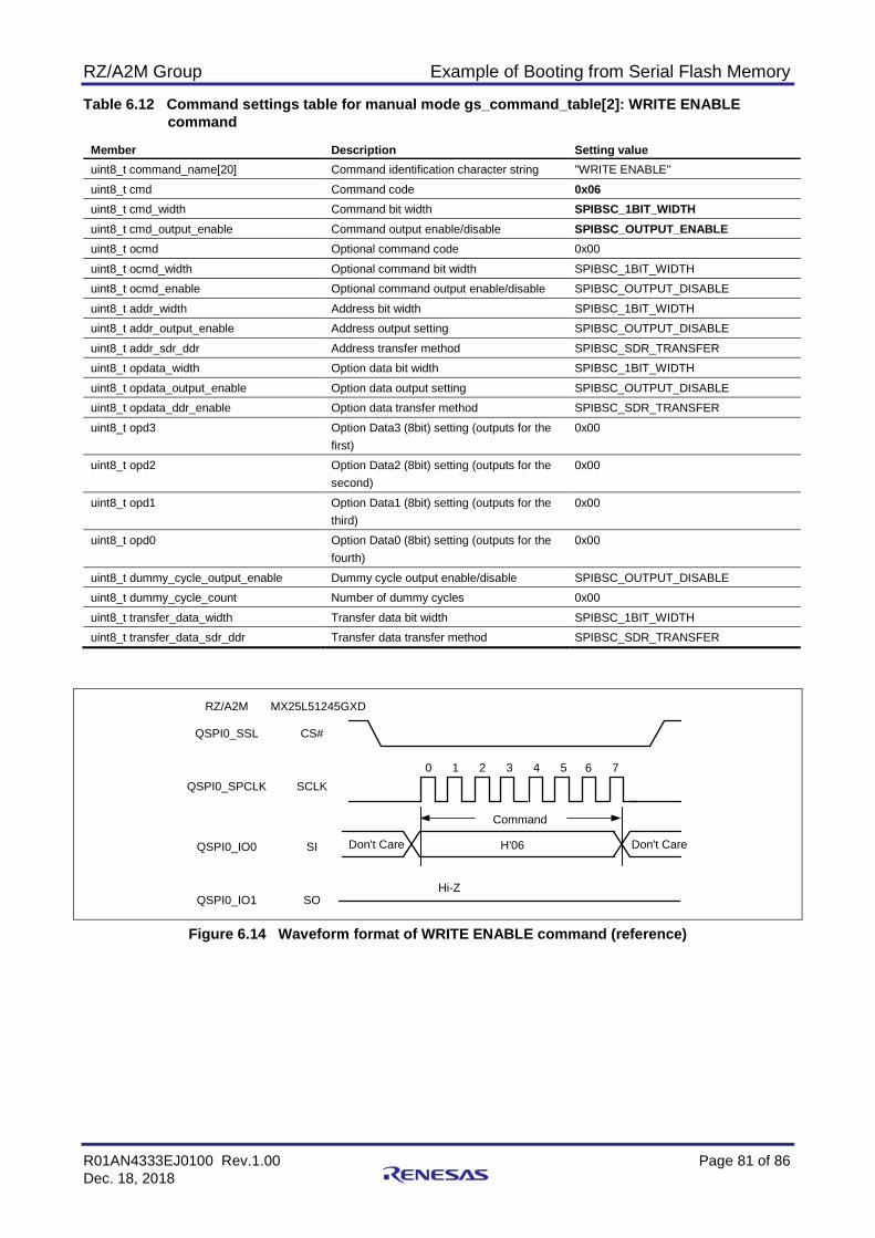
RZ/A2M Group Example of Booting from Serial Flash Memory
R01AN4333EJ0100 Rev.1.00 Page 81 of 86 Dec. 18, 2018
Table 6.12 Command settings table for manual mode gs_command_table[2]: WRITE ENABLE command
Member Description Setting value uint8_t command_name[20] Command identification character string "WRITE ENABLE" uint8_t cmd Command code 0x06 uint8_t cmd_width Command bit width SPIBSC_1BIT_WIDTH uint8_t cmd_output_enable Command output enable/disable SPIBSC_OUTPUT_ENABLE uint8_t ocmd Optional command code 0x00 uint8_t ocmd_width Optional command bit width SPIBSC_1BIT_WIDTH uint8_t ocmd_enable Optional command output enable/disable SPIBSC_OUTPUT_DISABLE uint8_t addr_width Address bit width SPIBSC_1BIT_WIDTH uint8_t addr_output_enable Address output setting SPIBSC_OUTPUT_DISABLE uint8_t addr_sdr_ddr Address transfer method SPIBSC_SDR_TRANSFER uint8_t opdata_width Option data bit width SPIBSC_1BIT_WIDTH uint8_t opdata_output_enable Option data output setting SPIBSC_OUTPUT_DISABLE uint8_t opdata_ddr_enable Option data transfer method SPIBSC_SDR_TRANSFER uint8_t opd3 Option Data3 (8bit) setting (outputs for the
first) 0x00
uint8_t opd2 Option Data2 (8bit) setting (outputs for the second)
0x00
uint8_t opd1 Option Data1 (8bit) setting (outputs for the third)
0x00
uint8_t opd0 Option Data0 (8bit) setting (outputs for the fourth)
0x00
uint8_t dummy_cycle_output_enable Dummy cycle output enable/disable SPIBSC_OUTPUT_DISABLE uint8_t dummy_cycle_count Number of dummy cycles 0x00 uint8_t transfer_data_width Transfer data bit width SPIBSC_1BIT_WIDTH uint8_t transfer_data_sdr_ddr Transfer data transfer method SPIBSC_SDR_TRANSFER
Figure 6.14 Waveform format of WRITE ENABLE command (reference)
CS#
SI
SO
SCLK
Hi-Z
H'06
Command
0 1 2 3 54 6 7
RZ/A2M MX25L51245GXD
QSPI0_SSL
QSPI0_IO0
QSPI0_IO1
QSPI0_SPCLK
Don't Care Don't Care

RZ/A2M Group Example of Booting from Serial Flash Memory
R01AN4333EJ0100 Rev.1.00 Page 82 of 86 Dec. 18, 2018
6.3.7 Serial Flash Memory Status/Configuration Register Write In the sample code, writing to the QE bit of the status register and DC[1:0] bits of the configuration register in the serial flash memory is executed with the Userdef_SPIBSC_SFLASH_WriteStatus function.
Implement the Userdef_SPIBSC_SFLASH_WriteStatus function according to the specifications of the serial flash memory to be used so that it can write the serial flash memory status register and configuration register settings.
Figure 6.15 shows the Userdef_SPIBSC_SFLASH_WriteStatus function processing flow of the sample code.
Figure 6.15 Userdef_SPIBSC_SFLASH_WriteStatus function processing flow
Userdef_SPIBSC_SFLASH_WriteStatus
return
Argument *p_status : Pointer to region in which the value written to the status register is stored *p_config : Pointer to region in which the value written to the configuration register is stored
The Write Status Register(WRSR[H'01]) command is issued for the serial flash memory.By setting the R_SPIBSC_SPICMDIssue function argument table_no to "3", the data in gs_command_table[3] which stores the data used to issue the Write Status Register command is used, and the SPI command issuing process is performed.
R_SPIBSC_SPICMDIssue function arguments 3 ( = table_no) : Use the gs_command_table[2] data when issuing command Arbitrary value ( = addr) : No effect on function processing &write_data[0] ( = *write_buff)
: The value for write_data[0](*p_status) is written to the Status Register: The value for write_data[1](*p_config) is written to the Configuration Register
2 ( = write_size) : Number of bytes written (2 bytes: *p_status, *p_config) Arbitrary value ( = *read_buff) : No effect on function processing Arbitrary value ( = read_size) : No effect on function processing
Wait until write is completedUserdef_SPIBSC_SFLASH_WatiReady()
Write Status Register (WRSR[H'01H])command issued
R_SPIBSC_SPICMDIssue()
Wait until the Write Status Registerr(WRSR[H'01]) command issuing has been completed.
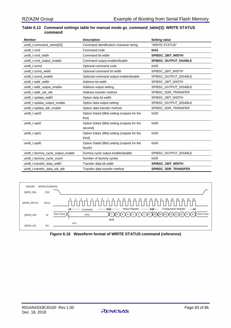
RZ/A2M Group Example of Booting from Serial Flash Memory
R01AN4333EJ0100 Rev.1.00 Page 83 of 86 Dec. 18, 2018
Table 6.13 Command settings table for manual mode gs_command_table[3]: WRITE STATUS command
Member Description Setting value uint8_t command_name[20] Command identification character string "WRITE STATUS" uint8_t cmd Command code 0x01 uint8_t cmd_width Command bit width SPIBSC_1BIT_WIDTH uint8_t cmd_output_enable Command output enable/disable SPIBSC_OUTPUT_ENABLE uint8_t ocmd Optional command code 0x00 uint8_t ocmd_width Optional command bit width SPIBSC_1BIT_WIDTH uint8_t ocmd_enable Optional command output enable/disable SPIBSC_OUTPUT_DISABLE uint8_t addr_width Address bit width SPIBSC_1BIT_WIDTH uint8_t addr_output_enable Address output setting SPIBSC_OUTPUT_DISABLE uint8_t addr_sdr_ddr Address transfer method SPIBSC_SDR_TRANSFER uint8_t opdata_width Option data bit width SPIBSC_1BIT_WIDTH uint8_t opdata_output_enable Option data output setting SPIBSC_OUTPUT_DISABLE uint8_t opdata_ddr_enable Option data transfer method SPIBSC_SDR_TRANSFER uint8_t opd3 Option Data3 (8bit) setting (outputs for the
first) 0x00
uint8_t opd2 Option Data2 (8bit) setting (outputs for the second)
0x00
uint8_t opd1 Option Data1 (8bit) setting (outputs for the third)
0x00
uint8_t opd0 Option Data0 (8bit) setting (outputs for the fourth)
0x00
uint8_t dummy_cycle_output_enable Dummy cycle output enable/disable SPIBSC_OUTPUT_DISABLE uint8_t dummy_cycle_count Number of dummy cycles 0x00 uint8_t transfer_data_width Transfer data bit width SPIBSC_1BIT_WIDTH uint8_t transfer_data_sdr_ddr Transfer data transfer method SPIBSC_SDR_TRANSFER
Figure 6.16 Waveform format of WRITE STATUS command (reference)
7 6 5 4 3 2 1 0 15 14 13 12 11 10 9 8
CS#
SI
SO
SCLK
Hi-Z
H'01
Command Status Register Configuration Register
MSB
0 1 2 3 54 6 7 8 9 1110 12 13 14 15 16 17 1918 20 21 22 23
RZ/A2M MX25L51245GXD
QSPI0_SSL
QSPI0_IO0
QSPI0_IO1
QSPI0_SPCLK
Don't Care Don't Care
RZ/A2M Group Example of Booting from Serial Flash Memory
R01AN4333EJ0100 Rev.1.00 Page 84 of 86 Dec. 18, 2018
7. Sample Code Precautions 7.1 Accessible area in external address space read mode The accessible area in external address space read mode is a 256MB area assigned to the SPI multi-IO bus space (H'2000_0000 to H'2FFF_FFFF). The SPIBSC converts access to this area to H'0000_0000 to H'0FFF_FFFF in the serial flash memory to access it. In the sample code, a 256MB area from H'0000_0000 to H'0FFF_FFFF in the serial flash memory can be accessed. In the RZ/A2M, an area larger than 256MB can be accessed by controlling the SPIBSC data read expansion address setting register (DREAR) and changing the serial flash memory address allocated to the SPI multi-I/O bus space, but since this prevents access to the area before DREAR is controlled, access to an area larger than 256MB is not supported in the sample code. The access specifications are only for H'0000_0000 to H'0FFF_FFFF in the serial flash memory.
In manual mode, access using a 4-byte address is supported, and a 4GB area of the serial flash memory can be accessed.
RZ/A2M Group Example of Booting from Serial Flash Memory
R01AN4333EJ0100 Rev.1.00 Page 85 of 86 Dec. 18, 2018
8. Sample Code Sample code can be downloaded from the Renesas Electronics website.
9. Reference Documents User's Manual: Hardware
RZ/A2M Group User's Manual: Hardware The latest version can be downloaded from the Renesas Electronics website.
RTK7921053C00000BE (RZ/A2M CPU board) User's Manual The latest version can be downloaded from the Renesas Electronics website. RTK79210XXB00000BE (RZ/A2M SUB board) User's Manual The latest version can be downloaded from the Renesas Electronics website.
Arm Architecture Reference Manual ARMv7-A and ARMv7-R edition Issue C The latest version can be downloaded from the Arm website.
Arm CortexTM-A9 Technical Reference Manual Revision: r4p1 The latest version can be downloaded from the Arm website. Arm Generic Interrupt Controller Architecture Specification - Architecture version2.0 The latest version can be downloaded from the Arm website.
Arm CoreLinkTM Level 2 Cache Controller L2C-310 Technical Reference Manual Revision: r3p3 The latest version can be downloaded from the Arm website.
Technical Update/Technical News
The latest information can be downloaded from the Renesas Electronics website. User's Manual: Integrated Development
The e2 studio Integrated Development Environment user's manual can be downloaded from the Renesas Electronics website. The latest version can be downloaded from the Renesas Electronics website.

RZ/A2M Group Example of Booting from Serial Flash Memory
R01AN4333EJ0100 Rev.1.00 Page 86 of 86 Dec. 18, 2018
Website and Support • Renesas Electronics website
http://www.renesas.com/ • Inquiries
http://www.renesas.com/contact/ All trademarks and registered trademarks are the property of their respective owners.

Revision History
Rev. Date Description Page Summary
Rev.1.00 Dec. 18, 2018 — First edition issued

General Precautions in the Handling of Microprocessing Unit and Microcontroller Unit Products The following usage notes are applicable to all Microprocessing unit and Microcontroller unit products from Renesas. For detailed usage notes on the products covered by this document, refer to the relevant sections of the document as well as any technical updates that have been issued for the products.
1. Handling of Unused Pins Handle unused pins in accordance with the directions given under Handling of Unused Pins in the manual. ¾ The input pins of CMOS products are generally in the high-impedance state. In operation with an
unused pin in the open-circuit state, extra electromagnetic noise is induced in the vicinity of LSI, an associated shoot-through current flows internally, and malfunctions occur due to the false recognition of the pin state as an input signal become possible. Unused pins should be handled as described under Handling of Unused Pins in the manual.
2. Processing at Power-on The state of the product is undefined at the moment when power is supplied. ¾ The states of internal circuits in the LSI are indeterminate and the states of register settings and
pins are undefined at the moment when power is supplied. In a finished product where the reset signal is applied to the external reset pin, the states of pins are not guaranteed from the moment when power is supplied until the reset process is completed. In a similar way, the states of pins in a product that is reset by an on-chip power-on reset function are not guaranteed from the moment when power is supplied until the power reaches the level at which resetting has been specified.
3. Prohibition of Access to Reserved Addresses Access to reserved addresses is prohibited. ¾ The reserved addresses are provided for the possible future expansion of functions. Do not access
these addresses; the correct operation of LSI is not guaranteed if they are accessed. 4. Clock Signals
After applying a reset, only release the reset line after the operating clock signal has become stable. When switching the clock signal during program execution, wait until the target clock signal has stabilized. ¾ When the clock signal is generated with an external resonator (or from an external oscillator)
during a reset, ensure that the reset line is only released after full stabilization of the clock signal. Moreover, when switching to a clock signal produced with an external resonator (or by an external oscillator) while program execution is in progress, wait until the target clock signal is stable.
5. Differences between Products Before changing from one product to another, i.e. to a product with a different part number, confirm that the change will not lead to problems. ¾ The characteristics of Microprocessing unit or Microcontroller unit products in the same group but
having a different part number may differ in terms of the internal memory capacity, layout pattern, and other factors, which can affect the ranges of electrical characteristics, such as characteristic values, operating margins, immunity to noise, and amount of radiated noise. When changing to a product with a different part number, implement a system-evaluation test for the given product.

http://www.renesas.comRefer to "http://www.renesas.com/" for the latest and detailed information.
Renesas Electronics CorporationTOYOSU FORESIA, 3-2-24 Toyosu, Koto-ku, Tokyo 135-0061, JapanRenesas Electronics America Inc.1001 Murphy Ranch Road, Milpitas, CA 95035, U.S.A.Tel: +1-408-432-8888, Fax: +1-408-434-5351Renesas Electronics Canada Limited9251 Yonge Street, Suite 8309 Richmond Hill, Ontario Canada L4C 9T3Tel: +1-905-237-2004Renesas Electronics Europe LimitedDukes Meadow, Millboard Road, Bourne End, Buckinghamshire, SL8 5FH, U.KTel: +44-1628-651-700Renesas Electronics Europe GmbHArcadiastrasse 10, 40472 Düsseldorf, Germany Tel: +49-211-6503-0, Fax: +49-211-6503-1327Renesas Electronics (China) Co., Ltd.Room 1709 Quantum Plaza, No.27 ZhichunLu, Haidian District, Beijing, 100191 P. R. ChinaTel: +86-10-8235-1155, Fax: +86-10-8235-7679Renesas Electronics (Shanghai) Co., Ltd.Unit 301, Tower A, Central Towers, 555 Langao Road, Putuo District, Shanghai, 200333 P. R. China Tel: +86-21-2226-0888, Fax: +86-21-2226-0999Renesas Electronics Hong Kong LimitedUnit 1601-1611, 16/F., Tower 2, Grand Century Place, 193 Prince Edward Road West, Mongkok, Kowloon, Hong KongTel: +852-2265-6688, Fax: +852 2886-9022Renesas Electronics Taiwan Co., Ltd.13F, No. 363, Fu Shing North Road, Taipei 10543, TaiwanTel: +886-2-8175-9600, Fax: +886 2-8175-9670Renesas Electronics Singapore Pte. Ltd.80 Bendemeer Road, Unit #06-02 Hyflux Innovation Centre, Singapore 339949Tel: +65-6213-0200, Fax: +65-6213-0300Renesas Electronics Malaysia Sdn.Bhd.Unit 1207, Block B, Menara Amcorp, Amcorp Trade Centre, No. 18, Jln Persiaran Barat, 46050 Petaling Jaya, Selangor Darul Ehsan, MalaysiaTel: +60-3-7955-9390, Fax: +60-3-7955-9510Renesas Electronics India Pvt. Ltd.No.777C, 100 Feet Road, HAL 2nd Stage, Indiranagar, Bangalore 560 038, IndiaTel: +91-80-67208700, Fax: +91-80-67208777Renesas Electronics Korea Co., Ltd.17F, KAMCO Yangjae Tower, 262, Gangnam-daero, Gangnam-gu, Seoul, 06265 KoreaTel: +82-2-558-3737, Fax: +82-2-558-5338
SALES OFFICES
© 2018 Renesas Electronics Corporation. All rights reserved.Colophon 7.2
(Rev.4.0-1 November 2017)
Notice1. Descriptions of circuits, software and other related information in this document are provided only to illustrate the operation of semiconductor products and application examples. You are fully responsible for
the incorporation or any other use of the circuits, software, and information in the design of your product or system. Renesas Electronics disclaims any and all liability for any losses and damages incurred by
you or third parties arising from the use of these circuits, software, or information.
2. Renesas Electronics hereby expressly disclaims any warranties against and liability for infringement or any other claims involving patents, copyrights, or other intellectual property rights of third parties, by or
arising from the use of Renesas Electronics products or technical information described in this document, including but not limited to, the product data, drawings, charts, programs, algorithms, and application
examples.
3. No license, express, implied or otherwise, is granted hereby under any patents, copyrights or other intellectual property rights of Renesas Electronics or others.
4. You shall not alter, modify, copy, or reverse engineer any Renesas Electronics product, whether in whole or in part. Renesas Electronics disclaims any and all liability for any losses or damages incurred by
you or third parties arising from such alteration, modification, copying or reverse engineering.
5. Renesas Electronics products are classified according to the following two quality grades: “Standard” and “High Quality”. The intended applications for each Renesas Electronics product depends on the
product’s quality grade, as indicated below.
"Standard": Computers; office equipment; communications equipment; test and measurement equipment; audio and visual equipment; home electronic appliances; machine tools; personal electronic
equipment; industrial robots; etc.
"High Quality": Transportation equipment (automobiles, trains, ships, etc.); traffic control (traffic lights); large-scale communication equipment; key financial terminal systems; safety control equipment; etc.
Unless expressly designated as a high reliability product or a product for harsh environments in a Renesas Electronics data sheet or other Renesas Electronics document, Renesas Electronics products are
not intended or authorized for use in products or systems that may pose a direct threat to human life or bodily injury (artificial life support devices or systems; surgical implantations; etc.), or may cause
serious property damage (space system; undersea repeaters; nuclear power control systems; aircraft control systems; key plant systems; military equipment; etc.). Renesas Electronics disclaims any and all
liability for any damages or losses incurred by you or any third parties arising from the use of any Renesas Electronics product that is inconsistent with any Renesas Electronics data sheet, user’s manual or
other Renesas Electronics document.
6. When using Renesas Electronics products, refer to the latest product information (data sheets, user’s manuals, application notes, “General Notes for Handling and Using Semiconductor Devices” in the
reliability handbook, etc.), and ensure that usage conditions are within the ranges specified by Renesas Electronics with respect to maximum ratings, operating power supply voltage range, heat dissipation
characteristics, installation, etc. Renesas Electronics disclaims any and all liability for any malfunctions, failure or accident arising out of the use of Renesas Electronics products outside of such specified
ranges.
7. Although Renesas Electronics endeavors to improve the quality and reliability of Renesas Electronics products, semiconductor products have specific characteristics, such as the occurrence of failure at a
certain rate and malfunctions under certain use conditions. Unless designated as a high reliability product or a product for harsh environments in a Renesas Electronics data sheet or other Renesas
Electronics document, Renesas Electronics products are not subject to radiation resistance design. You are responsible for implementing safety measures to guard against the possibility of bodily injury, injury
or damage caused by fire, and/or danger to the public in the event of a failure or malfunction of Renesas Electronics products, such as safety design for hardware and software, including but not limited to
redundancy, fire control and malfunction prevention, appropriate treatment for aging degradation or any other appropriate measures. Because the evaluation of microcomputer software alone is very difficult
and impractical, you are responsible for evaluating the safety of the final products or systems manufactured by you.
8. Please contact a Renesas Electronics sales office for details as to environmental matters such as the environmental compatibility of each Renesas Electronics product. You are responsible for carefully and
sufficiently investigating applicable laws and regulations that regulate the inclusion or use of controlled substances, including without limitation, the EU RoHS Directive, and using Renesas Electronics
products in compliance with all these applicable laws and regulations. Renesas Electronics disclaims any and all liability for damages or losses occurring as a result of your noncompliance with applicable
laws and regulations.
9. Renesas Electronics products and technologies shall not be used for or incorporated into any products or systems whose manufacture, use, or sale is prohibited under any applicable domestic or foreign laws
or regulations. You shall comply with any applicable export control laws and regulations promulgated and administered by the governments of any countries asserting jurisdiction over the parties or
transactions.
10. It is the responsibility of the buyer or distributor of Renesas Electronics products, or any other party who distributes, disposes of, or otherwise sells or transfers the product to a third party, to notify such third
party in advance of the contents and conditions set forth in this document.
11. This document shall not be reprinted, reproduced or duplicated in any form, in whole or in part, without prior written consent of Renesas Electronics.
12. Please contact a Renesas Electronics sales office if you have any questions regarding the information contained in this document or Renesas Electronics products.
(Note 1) “Renesas Electronics” as used in this document means Renesas Electronics Corporation and also includes its directly or indirectly controlled subsidiaries.
(Note 2) “Renesas Electronics product(s)” means any product developed or manufactured by or for Renesas Electronics.