rtl hardware design by p. chu chapter 161 clock and synchronization
TRANSCRIPT

RTL Hardware Design by P. Chu
Chapter 16 1
Clock and Synchronization

RTL Hardware Design by P. Chu
Chapter 16 2
Outline
1. Why synchronous?
2. Clock distribution network and skew
3. Multiple-clock system
4. Meta-stability and synchronization failure
5. Synchronizer

RTL Hardware Design by P. Chu
Chapter 16 3
1. Why synchronous

RTL Hardware Design by P. Chu
Chapter 16 4
Timing of a combinational digital system
• Steady state– Signal reaches a stable value – Modeled by Boolean algebra
• Transient period– Signal may fluctuate – No simple model
• Propagation delay: time to reach the steady state

RTL Hardware Design by P. Chu
Chapter 16 5
Timing Hazards
• Hazards: the fluctuation occurring during the transient period – Static hazard: glitch when the signal should
be stable– Dynamic hazard: a glitch in transition
• Due to the multiple converging paths of an output port

RTL Hardware Design by P. Chu
Chapter 16 6
• E.g., static-hazard (sh=ab’+bc; a=c=1)

RTL Hardware Design by P. Chu
Chapter 16 7
• E.g., dynamic hazard (a=c=d=1)

RTL Hardware Design by P. Chu
Chapter 16 8
E.g., Hazard of circuit with closed feedback loop (async seq circuit)

RTL Hardware Design by P. Chu
Chapter 16 9

RTL Hardware Design by P. Chu
Chapter 16 10
Dealing with hazards• In a small number of cases, additional logic can
be added to eliminate race (and hazards).

RTL Hardware Design by P. Chu
Chapter 16 11
• This is not feasible for synthesis
• What’s can go wrong:– During logic synthesis, the logic expressions
will be rearranged and optimized.– During technology mapping, generic gates will
be re-mapped– During placement & routing, wire delays may
change– It is bad for testing verification

RTL Hardware Design by P. Chu
Chapter 16 12
• Important Timing Parameters in Flip-Flops
Tcq: clock-to-q delay, is the propagation delay required for the d input to show up at the q output after the sampling edge of the clock (rising or falling edge).
Tsetup: setup time, the time interval in which the d signal must be stable before the clock edge arrives.
Thold: hold time, the time interval in which the d signal must be stable after the clock edge.

RTL Hardware Design by P. Chu
Chapter 16 13
• Better way to handle hazards– Ignore glitches in the transient period and retrieve
the data after the signal is stabilized
• In a sequential circuit– Use a clock signal to sample the signal and store
the stable value in a register.– But register introduces new timing constraint (setup
time and hold time)

RTL Hardware Design by P. Chu
Chapter 16 14
• Synchronous system:– group registers into a single group and drive
them with the same clock– Timing analysis for a single feedback loop

RTL Hardware Design by P. Chu
Chapter 16 15
Synchronous circuit and EDA
• Synthesis: reduce to combinational circuit synthesis
• Timing analysis: involve only a single closed feedback loop (others reduce to combinational circuit analysis)
• Simulation: support “cycle-based simulation”
• Testing: can facilitate scan-chain
RTL Hardware Design by P. Chu
Chapter 16 16
2. Clock distribution network and skew

RTL Hardware Design by P. Chu
Chapter 16 17
Clock distribution network
• Ideal clock: clock’s rising edges arrive at FFs at the same time
• Real implementation: – Driving capability of each cell is limited – Need a network of buffers to drive all FFs– In ASIC: done by clock synthesis (a step in
physical synthesis)– In FPGA: pre-fabricated clock distribution
network

RTL Hardware Design by P. Chu
Chapter 16 18
• Block diagram • Ideal H-routing
RTL Hardware Design by P. Chu
Chapter 16 19
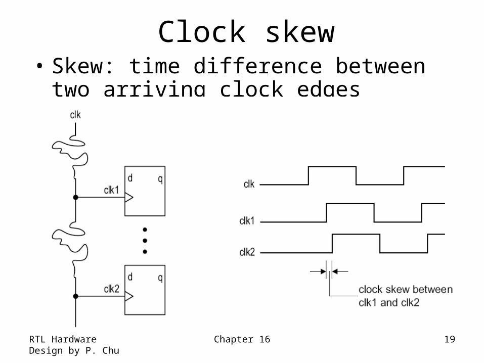
Clock skew• Skew: time difference between two
arriving clock edges
RTL Hardware Design by P. Chu
Chapter 16 20
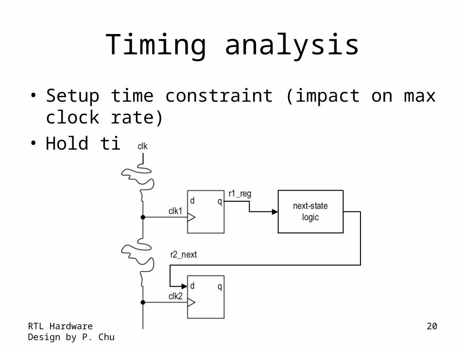
Timing analysis
• Setup time constraint (impact on max clock rate)• Hold time constraint

RTL Hardware Design by P. Chu
Chapter 16 21

RTL Hardware Design by P. Chu
Chapter 16 22
• Clock skew actually helps increasing clock rate in this particular case

RTL Hardware Design by P. Chu
Chapter 16 23
• If the clock signal travels from the opposite direction
• Normally we have to consider the worst case since– No control on clock routing during synthesis– Multiple feedback paths