roxtm ingaas avalanche laser ranging photodiode (apd) and lidar … · 2019-04-12 · roxtm ingaas...
TRANSCRIPT
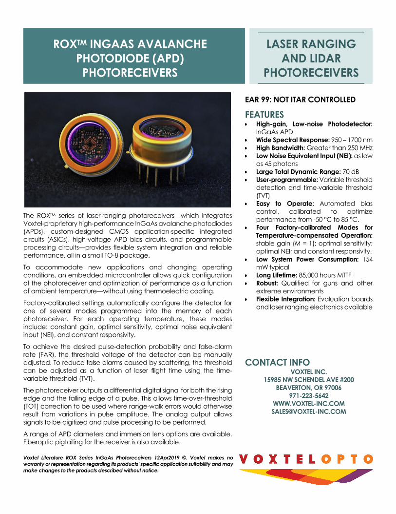
ROXTM INGAAS AVALANCHE PHOTODIODE (APD) PHOTORECEIVERS
LASER RANGING AND LIDAR
PHOTORECEIVERS
The ROXTM series of laser-ranging photoreceivers—which integrates Voxtel-proprietary high-performance InGaAs avalanche photodiodes (APDs), custom-designed CMOS application-specific integrated circuits (ASICs), high-voltage APD bias circuits, and programmable processing circuits—provides flexible system integration and reliable performance, all in a small TO-8 package.
To accommodate new applications and changing operating conditions, an embedded microcontroller allows quick configuration of the photoreceiver and optimization of performance as a function of ambient temperature—without using thermoelectric cooling.
Factory-calibrated settings automatically configure the detector for one of several modes programmed into the memory of each photoreceiver. For each operating temperature, these modes include: constant gain, optimal sensitivity, optimal noise equivalent input (NEI), and constant responsivity.
To achieve the desired pulse-detection probability and false-alarm rate (FAR), the threshold voltage of the detector can be manually adjusted. To reduce false alarms caused by scattering, the threshold can be adjusted as a function of laser flight time using the time-variable threshold (TVT).
The photoreceiver outputs a differential digital signal for both the rising edge and the falling edge of a pulse. This allows time-over-threshold (TOT) correction to be used where range-walk errors would otherwise result from variations in pulse amplitude. The analog output allows signals to be digitized and pulse processing to be performed.
A range of APD diameters and immersion lens options are available. Fiberoptic pigtailing for the receiver is also available.
EAR 99: NOT ITAR CONTROLLED
FEATURES High-gain, Low-noise Photodetector:
InGaAs APD Wide Spectral Response: 950 – 1700 nm High Bandwidth: Greater than 250 MHz Low Noise Equivalent Input (NEI): as low
as 45 photons Large Total Dynamic Range: 70 dB User-programmable: Variable threshold
detection and time-variable threshold (TVT)
Easy to Operate: Automated bias control, calibrated to optimize performance from -50 °C to 85 °C.
Four Factory-calibrated Modes for Temperature-compensated Operation: stable gain (M = 1); optimal sensitivity; optimal NEI; and constant responsivity.
Low System Power Consumption: 154 mW typical
Long Lifetime: 85,000 hours MTTF Robust: Qualified for guns and other
extreme environments Flexible Integration: Evaluation boards
and laser ranging electronics available
CONTACT INFO VOXTEL INC.
15985 NW SCHENDEL AVE #200 BEAVERTON, OR 97006
971-223-5642 WWW.VOXTEL-INC.COM [email protected]
Voxtel Literature ROX Series InGaAs Photoreceivers 12Apr2019 ©. Voxtel makes no warranty or representation regarding its products’ specific application suitability and may make changes to the products described without notice.

2
Specifications Performance RUC1-JIAC RUC1-NIAC RUC1-KIAC
Spectral response,1 λ 950 nm – 1700 nm Optical collection-area diameter2 75 μm 200 μm 250 μm3 APD diameter2 75 μm 200 μm 75 μm Noise equivalent input (NEI)1,4,5,6,7 45 photons 45 photons 45 photons Photon equivalent sensitivity4,8 245 photons 290 photons 245 photons Noise equivalent power1,6,7,9 0.20 nW 0.45 nW 0.20 nW Range precision1,4,6,10 50 mm 60 mm 50 mm Target pair resolution1,10 5 meters 5 meters 5 meters Bandwidth1,11 275 MHz 257 MHz 275 MHz Cuton frequency11 4.74 kHz 4.66 kHz 4.52 kHz APD gain (M)1 1 – 20 1 – 20 1 – 20 APD responsivity (M = 1)6 1.1 A/W 1.1 A/W 1.1 A/W APD excess noise (M = 10)1,12,13 3.50 3.50 3.50 Maximum instantaneous optical power1,6,14 6 MW/cm2
Factory-calibrated Operating Modes15,16
START Pulse Length Program Description
1 125 µs ±10 µs M = 1 2 150 µs ±10 µs Optimal gain for ~10 – 350-Hz FAR (calibrated at 150-Hz FAR) 3 200 µs ±10 µs Optimal gain to achieve best NEI at each temperature 4 175 µs ±10 µs Not specified or custom configured17
Digital Output2 Comparator threshold useable range 0.45 V – 1.0 V Time-variable threshold (TVT) decay time 2.6 μs Dynamic range, linear 25 dB Dynamic range, total 70 dB Analog Output1,2,4,12,18 Max small signal responsivity19 8,620 kV/W 8,620 kV/W 8,620 kV/W Analog output noise 1.07 mV RMS 1.37 mV RMS 1.07 mV RMS Analog output swing 0.186 V 0.186 V 0.186 V Analog output dynamic range 7.4 bits 7.1 bits 7.4 bits Power Requirements—Threshold Levels2 Low-voltage circuits, 1.8 V APD supply 8.1 mA Low-voltage circuits, 5 V APD supply 1.5 mA High-voltage (HV) circuits, < 63 V APD supply 2.2 mA Power consumption, standby/ranging (HV off/HV on) 22 mW / 154 mW Environmental1 Operational temperature range -50 °C to +85 °C
1 Sampled from manufacturing data (available upon request)
2 Based on eng. design analysis supported by experimental data
3 At input to hemispheric BK7 immersion (500 µm dia.) lens
4 4-ns pulse length 5 Optimal gain 6 1534-nm spectral response 7 25 °C 8 60-Hz FAR, 50% PDE
9 20-ns pulse length 10 5x NEI photon pulse amplitude 11 Bandwidth over which conversion gain is
greater than 200 kV/W (at M = 10) 12 Gain: M = 10 13 keff < 0.18 parameterization of McIntyre
Equation: F(M) = keff M + (1 – keff)(2 – 1/M) 14 Gain of M = 1 15 Specifications are included w/Cert. of
Conformance w/each APD
16 All parts temperature-compensated for performance over op. temp. range; beyond this range, analytical approximations are used to compensate photoreceiver for optimal performance
17 At high temp in constant responsivity mode dark counts may saturate the receiver
18 50Ω load 19 Gain of M = 20 is assumed
3
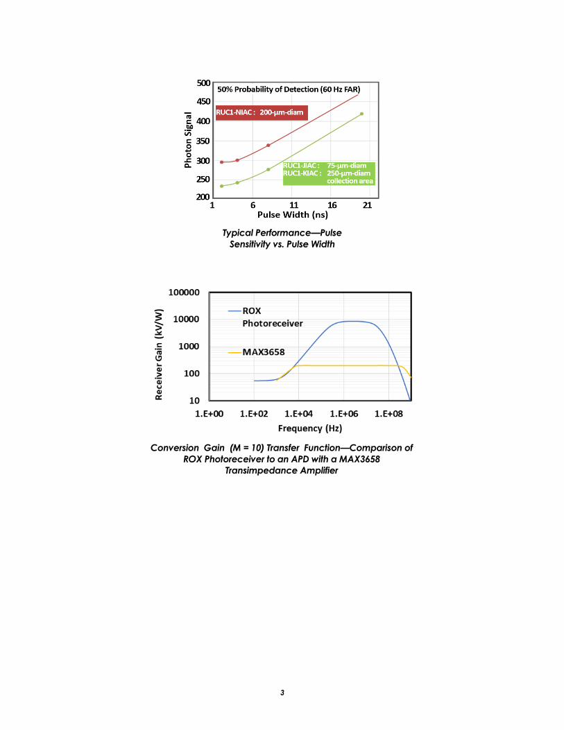
Typical Performance—Pulse Sensitivity vs. Pulse Width
Conversion Gain (M = 10) Transfer Function—Comparison of ROX Photoreceiver to an APD with a MAX3658
Transimpedance Amplifier
4
Ordering Information
Standalone/Integrated Receivers In addition to the standalone TO-8 packages*, the ROX InGaAs APD Photoreceivers are available integrated with fiber or integrated with time-of-flight (TOF) and control electronics. These options are also available without receiver integration—as standalone support components.
TO-8 Packaged APD Receiver* Plus:
APD Size - (Standalone)
62.5/125 µm (0.27 NA) Fiber
Coupling†
105/125 µm (0.22 NA) Fiber
Coupling‡
200 µm (0.37 NA) Fiber
Coupling§ Shipped with TOF & Control Electronics‖
75 µm RUC1-JIAC - - - EU0K-J00C 200 µm RUC1-NIAC RUC1-NIQC RUC1-NIRC RUC1-NITC EU0K-N00C
250 µm CA¶ RUC1-KIAC - - RUC1-KITC EU0K-K00C 500 µm RUC1-PIAC - - - EU0K-P00C
* includes integrated pulse-detection ASIC & APD size indicated † 62.5-µm-core/125-µm-clad (0.27 NA) FC/PC fiber pigtail ‡ 105-µm-core/125-µm-clad (0.22 NA) FC/PC fiber pigtail § 200-µm-core (0.37 NA) FC/PC fiber pigtail
‖ TO-8 packaged APD receiver* is mounted to a socket board with time-of-flight and control electronics. For unintegrated
¶ 250-µm collection area immersion-lensed APD
Standalone Support Components (TO-8 Packaged APD Receiver Not Included) These standalone support components are intended for use with the above standalone ROX InGaAs APD photoreceivers; photoreceivers are not included.
Standalone Support Component (TO-8 Packaged APD Receiver Not Included)) Part Number Photoreceiver evaluation board WRR0A
Photoreceiver socket board with Time-of-flight & control electronics** EU0K-X00C
** This is equivalent to the TOF & Control Electronics option above (see Standalone/Integrated Receivers‖) without the TO-8 Packaged APD Receiver above (see Standalone/Integrated Receivers*).
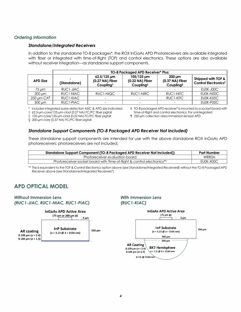
APD OPTICAL MODEL
Without Immersion Lens (RUC1-JIAC, RUC1-NIAC, RUC1-PIAC)
With Immersion Lens (RUC1-KIAC)
5
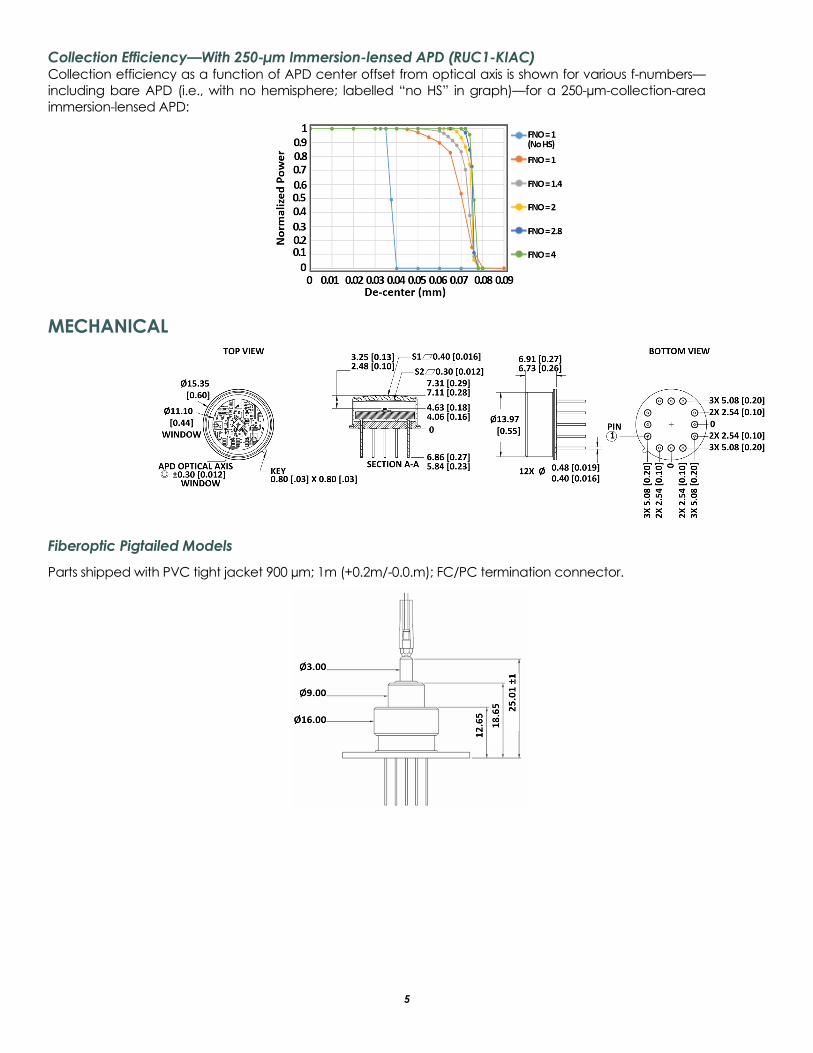
Collection Efficiency—With 250-µm Immersion-lensed APD (RUC1-KIAC) Collection efficiency as a function of APD center offset from optical axis is shown for various f-numbers— including bare APD (i.e., with no hemisphere; labelled “no HS” in graph)—for a 250-µm-collection-area immersion-lensed APD:
MECHANICAL
Fiberoptic Pigtailed Models Parts shipped with PVC tight jacket 900 µm; 1m (+0.2m/-0.0.m); FC/PC termination connector.
6
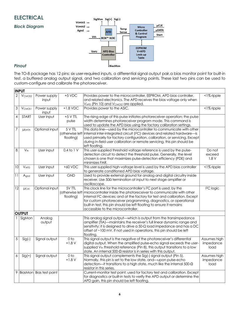
ELECTRICAL Block Diagram
Pinout The TO-8 package has 12 pins: six user-required inputs, a differential signal output pair, a bias monitor point for built-in test, a buffered analog output signal, and two calibration and servicing points. These last two pins can be used to custom-configure and calibrate the photoreceiver.
INPUT 2 VCMOS2 Power supply
input +5 VDC Provides power to the microcontroller, EEPROM, APD bias controller,
and related electronics. The APD receives the bias voltage only when VAPD (Pin 10) and VCMOS2 are applied.
<1% ripple
3 VCMOS1 Power supply input
+1.8 VDC Provides power to the ASIC. <1% ripple
4 START User input +5 V TTL pulse
The rising edge of this pulse initiates photoreceiver operation; the pulse width determines photoreceiver program mode. This command is used to update the APD bias using the factory calibration settings.
7 μDATA Optional input 5 V TTL (otherwise left
floating)
This data line—used by the microcontroller to communicate with other internal inter-integrated circuit (I2C) devices and related hardware—is used primarily for factory configuration, calibration, or servicing. Except during in-field user calibration or remote servicing, this pin should be left floating.
8 Vth User input 0.4 to 1 V This user-supplied threshold voltage reference is used by the pulse-detection circuit to detect the threshold pulse. Generally, the level chosen is one that maximizes pulse-detection efficiency (PDE) and minimizes FAR.
Do not exceed
1.8 V
10 VAPD User input +60 VDC This user-supplied high-voltage level is used by the APD bias controller to generate conditioned APD bias voltage.
<1% ripple
11 Agnd User input GND Used to provide external ground for analog and digital circuitry inside receiver. Use 50Ω termination at input to next stage amplifier or oscilloscope.
12 μCLK Optional input 5V TTL (otherwise left
floating)
This clock line for the microcontroller’s I2C port is used: by the microcontroller inside the photoreceiver to communicate with other internal I2C devices; and at the factory for test and calibration. Except for custom photoreceiver programming, diagnostics, or operational built-in test, this pin should be left floating to ensure it remains accessible to the microcontroller.
I2C logic
OUTPUT 1 SigMon Analog
output This analog signal output—which is output from the transimpedance
amplifier (TIA)—maintains the receiver’s full linear dynamic range and sensitivity; it is designed to drive a 50-Ω load impedance and has a DC offset of ~100 mV. If not used in operations, this pin should be left floating.
5 Sig(-) Signal output 0 to +1.8 V
This signal output is the negative of the photoreceiver’s differential digital output. When the amplified pulse-echo signal exceeds the user-supplied Vth threshold reference (Pin 8), this output transitions to a low state. An internal 500-Ω resistor is in series with this output.
Assumes high impedance
load
6 Sig(+) Signal output 0 to +1.8 V
This signal output complements the Sig(-) signal output (Pin 5). Normally, this pin is set to the low state, and—upon pulse-echo detection—it transitions to a high state, much like the internal 500-Ω resistor in this series.
Assumes high impedance
load
9 BiasMon Bias test point Current-monitor test point; used for factory test and calibration. Except for diagnostics or built-in tests to verify the APD output or determine the APD gain, this pin should be left floating.
7
ROX PHOTORECEIVER OPERATION Provisioning Power When VCMOS1, VCMOS2, and VAPD are applied, the microcontroller starts its clock, enters the run state, measures the APD temperature, sets the APD gain to M = 1 (mode 1), then enters the sleep state. These biases may be applied to the chip in any order without risking any damage to the receiver. The photoreceiver is then ready to operate and will begin to detect pulses upon receipt of the range command.
Signal Amplification and Pulse Detection The ROX receiver integrates a Voxtel-proprietary InGaAs APD sensitive over the 950-nm to 1700-nm spectral range with stable avalanche gain up to M = 20. For most conditions, the operational optimum is achieved at lower gain.
The excess noise of the APD is characterized by McIntyre parameterization of k < 0.18. The avalanche-multiplied signal from the APD is processed by a custom Voxtel-designed ASIC. The ASIC includes a two-stage resistive TIA that converts the APD’s output current into an amplified voltage signal that is fed to a leading-edge pulse discriminator; the threshold voltage reference level, Vth, is user-supplied. To prevent false triggering from unwanted returns during the initial pulse-transmission period, a time-variable-threshold function is available. The Vth threshold bias includes an RC circuit, which allows for temporal decay of the threshold for about 2.6 µs following application of the threshold voltage.
Upon detecting a signal, the pulse-detection circuit generates a differential output pulse [Sig(+) and Sig(-)] with a duration proportional to the pulse amplitude. Because a proportional logic signal is output for both the leading edge and the falling edge of the pulse-amplitude signal, time-over-threshold (TOT) correction is enabled. This allows correction for amplitude-dependent timing variation. Using the TOT duration, correction of range-walk errors is enabled up to a 70-dB range of signal amplitudes.
The buffered analog signal is also available as an output. The buffered output signal can be sampled or digitized for use in false-alarm rejection and signal processing.
Time-variable Threshold (TVT) To reduce the susceptibility of triggering from foreground pulse returns, the ROX receiver can be configured for time-variable threshold via a factory-configured RC filter circuit in the photoreceiver.
When the external value of Vth is changed from one value to another—e.g., from a high voltage level, Vth,hi, to a low voltage level, Vth,lo—the internal threshold Vth(τ) changes according to the RC time constant of 2.6 μs (102-kΩ resistor and 25.5-pF capacitor). The time constant changes the threshold as follows:
Vth (τ) = Vth,hi- (Vth,hi – Vth,lo)·e-τ⁄R·C
where Vth,hi is the initial threshold value, and Vth,lo is the final desired threshold value.
APD Bias and Temperature Compensation WARNING: If the bias is held constant, changes in temperature will cause avalanche gain levels to vary. If the
temperature of the APD is less than it was during calibration, higher overall avalanche gain will likely result. This can cause the APD to be biased above the avalanche breakdown voltage. For this reason, it is critical to start the device in a stable-gain mode (e.g., operating mode 1, where M = 1) and to command APD bias compensation regularly during operation. Otherwise, the sustained avalanche breakdown currents may damage the APD.
APD gain changes with temperature. To avoid the complications associated with thermoelectric coolers (TECs), such as power draw and cost, the ROX series of photoreceivers uses a temperature-dependent bias-compensation scheme, where—for each of the four factory-calibrated modes—APD biases at temperatures throughout the operational range are factory-programmed in the photoreceiver. State-machine control—including temperature sensing and gain compensation—are performed using a Microchip PIC12F series microcontroller (www.microchip.com) integrated in the TO-8 package.
The APD bias is updated with the pulse-width-encoded START signal. Each time the START signal is sent, the photoreceiver measures the temperature and updates the APD bias for the selected operating mode. The APD bias controller generates a conditioned bias voltage for the APD using signals from the microcontroller to achieve the
8
desired avalanche gain using the most recent temperature measurement. Provided that the user-supplied bias (VAPD) is present at the appropriate input pin of the photoreceiver, the microcontroller sends a signal to the 10-bit digital-to-analog converter (DAC), which biases the input to the APD bias controller. The bias controller amplifies the input voltage from the DAC by a factor of 30 and applies it to the APD. The DAC provides a maximum APD bias voltage variation of 146 mV.
to achieve stable operating and to avoid damage to the APD, the START command should be sent regularly during operation—preferably before every measurement taken. The breakdown voltage of the APD changes about 33 mV/°C. Avalanche gain drops as temperature rises, and rises as temperature drops. Thus, updating the APD bias regularly with the factory temperature-calibrated APD bias settings allows stable photoreceiver operation.
Due to temperature-dependent APD gain, if the START command is not used to calibrate the APD for the ambient temperature, the APD may be caused to be biased above the breakdown voltage, which will cause damage to the detector. This can occur, for instance, when the APD is calibrated last at a high operating temperature, and is not updated using the START command as the operating temperature drops. As the APD gain increases at colder temperatures, the APD can then enter into avalanche breakdown, which will damage the APD. Thus, periodic update of the calibration is required using the START command.
PHOTORECEIVER OPERATING MODES Factory Calibration The microcontroller is configured at the factory with four user-selectable programs stored in a look-up table in the photoreceiver. The microcontroller uses the look-up table to determine the APD bias voltage for the user-selected operating mode. Each operating mode provides automatic temperature compensation of multiplication gain by adjusting the reverse bias on the APD. The microcontroller can also be custom-programmed with custom startup sequences and operating schemes.
The photoreceiver can be set to any of the factory-configured operating modes programmed in the microcontroller. To select the desired operating mode, the START signal to the APD is applied for the duration specific to the desired operating mode, and a pulse-width-encoded signal is sent to the microcontroller. Upon receipt of the START command, the microcontroller measures the temperature of the APD, and—based on the user-provided pulse-width-encoded value—uses the temperature reading to address the look-up table to determine the optimal APD bias for the selected operating mode.
Constant Gain: APD gain decreases as temperature increases, and increases as temperature decreases. Thus, to maintain a constant gain, the APD bias must be adjusted as the operating temperature changes. The APD bias is calibrated at the factory so that—at each specified temperature—the bias necessary to achieve the specified gain is used to operate the detector. To minimize damage to the photoreceiver due to high laser pulse energies, a bias setting of M = 1 is recommended when first powering-on the photoreceiver. For most ROX receiver models, the bias conditions for M = 1 are included in the factory calibration as Mode 1.
Optimal Sensitivity: Each ROX photoreceiver is calibrated at the factory by operating the photoreceiver without any optical signal—that is, in the dark. At each temperature, an automatic optimization routine uses a digital counter to measure the false alarms present at a threshold that achieves a 50% probability of detecting an optical signal at the specified false-alarm rate. At each temperature, the bias that results in the best photon-equivalent sensitivity is stored in the photoreceiver memory. In general, when using this operating mode: At high temperatures, to reduce FAR contributions due to APD dark current, gain is reduced; at low temperature, to compensate for limited photoreceiver sensitivity resulting from ASIC noise (as opposed to noise from APD dark current), the APD gain is increased. The required FAR is generally application specific and can be estimated using the relationship FAR = (c*Pfa)/ (2*R), where Pfa is the probability of a false alarm; C is the speed of light (3 x 10⁸ m/s), and R is the maximum target range in meters (e.g., for a target Pfa of 0.25% at a maximum range of 2.5 km, the target FAR is 150 Hz). When in use, upon user command, the APD biases are updated for the current operating temperature. Using the factory-configured biases, when in use, the FAR contributions from background optical radiation (e.g., solar contribution) can be measured by operating the photoreceiver without any laser pulses, and the threshold can be adjusted to achieve the desired FAR in the presence of background radiation. This allows the ROX photoreceiver to be dynamically optimized for operational requirements.
Optimal Noise Equivalent Input (NEI) / Optimal Noise Equivalent Power (NEP): In this mode of operation, to calibrate the photoreceiver, for each gain, the threshold is swept over its full voltage range without illumination. The plot of the
9
measured count rate at each bias, is fit to a cumulative distribution function (CDF) of a normal distribution. The photon count of the normal distribution that results in the best fit to the measured values, is the noise equivalent input (NEI). The NEI measured at each avalanche gain is calculated over the temperature range, and the gain values that result in the lowest NEI are stored in each ROX APD photoreceiver after factory calibration.
Constant Responsivity (Normalized to the Gain that Results in the Best NEI at 25 °C): The calibration for this operating mode is similar to those above. However, rather than optimizing the gain for each temperature, the APD gain that allows for the best NEI at 25 °C is determined, and the APD gain is compensated at each operating temperature so that responsivity is constant over the operating temperature range. The constant responsivity mode reaches saturation at high and low operating temperatures, so the constant responsivity is achieved over a smaller temperature range than the specified receiver operating temperature range.
Selecting Operating Modes The receiver is biased in the OFF condition when the power to the photoreceiver is removed. In this mode, the biases are removed from VCMOS1, VCMOS2, and VAPD in any sequence. To protect the APD from large signals, VAPD may also be powered off separately. For operation, the desired operating mode is selected by applying the START signal for the duration listed in the START Pulse Width column of the specifications table. Each mode requires 15 ms to set up before operation can resume. A brief description of each program mode follows:
Mode 1: With the application of VCMOS1, VCMOS2, and VAPD, the microcontroller starts its clock, enters the run state, measures the APD temperature, sets the APD gain to M = 1, then enters the sleep state. These biases may be applied to the chip in any order without risking any damage to the receiver.
All Other Modes (i.e., 2 – 4): The APD bias is established within 15 ms of receiving the START signal. After receiving the START signal, the microcontroller digitizes the value from the temperature sensor using the internal 10-bit analog-to-digital converter (ADC). This temperature measurement is used to address the look-up tables stored in the EEPROM for the selected operating mode. The contents of the look-up table are used to set the appropriate APD bias voltage for the measured temperature. Once the voltage is set, the microcontroller again enters a sleep state, wherein all digital switching, including the internal clock, are stopped to reduce digital noise coupling to the analog signal chain. With the microcontroller in the sleep state, the receiver operates in the current mode until the next START pulse is received.
RANGE PRECISION Using the speed of light, lidar sensors calculate the distance of an object using the equation: Range = (Speed of light × time of flight of laser pulse) ÷ 2. The range precision can be calculated similarly. For example, achieving a 2-cm range precision requires timestamps with resolution of about 133 ps.
To maximize performance over a wide dynamic range, the photoreceiver is configured with a leading-edge pulse-discriminating detection circuit. The ASIC’s comparator receives the input optical pulse, then—when the leading edge of the pulse crosses the input threshold voltage value (Vth,int)—generates a signal. In the absence of noise and amplitude variations, the leading-edge discriminator marks the arrival time of each analog pulse with precision and consistency. Electronic noise causes an uncertainty—or jitter—when the analog pulse crosses the discriminator threshold, which determines the range precision. In general, higher operating gain and larger signals result in better timing precision.
PULSE-PAIR RESOLUTION Pulse-pair resolution is defined here as the minimum time between target returns that can be recorded. The ROX generates a minimum output pulse width of 7 nanoseconds, which—in combination with the time-to-digital converter (TDC)—limits the pulse-pair resolution to no better than about 0.5 meters. Voxtel designed the ROX photoreceiver to accommodate optical power levels varying up to 70 dB. In this range, the photoreceiver recovers from a pulse within 70 ns (about 10 meters), and is again ready to receive optical pulses. Over the linear part of the response—when the analog signal is not saturated, about 20 dB—the pulse-pair resolution is better than 5 meters.
RANGE-PRECISION ENHANCEMENT USING TIME-OVER-THRESHOLD CORRECTION Range walk is the systematic dependence of the timing on the input pulse amplitude. With a leading-edge timing discriminator, smaller pulses produce an output from the discriminator later than larger pulses, leading to variable timing in response to variations in input pulse amplitudes. For scenarios in which a wide range of pulse amplitudes are

10
received, range-walk errors due to signal strength can seriously degrade the timing accuracy. Thus, to ensure accurate range timing, range walk must be minimized or eliminated. To mitigate the effects of range walk, the ROX includes a time-over-threshold (TOT) feature, where the times of the pulse’s leading-edge and falling-edge threshold crossings are used to compute the TOT. To calculate TOT, the time of the leading-edge event is subtracted from that of the falling-edge event; the resulting TOT is proportional to the pulse amplitude. To mitigate range-walk errors resulting from variations in pulse signal strength, TOT can be calibrated for the range of anticipated pulse amplitudes.
Range-walk error and TOT at the output of the receiver is shown as a function of the input signal amplitude.
The range walk (time walk) and measured digital output pulse width (time over threshold) plotted as a function of
input signal pulse amplitude. The plot shows values corrected using a bilinear approximation and using a calibrated look-up table. Here, the bilinear equations are y = -0.234x – 15.79 for TOT values below 27 ns, and y = -0.035x – 9.11
for TOT values higher than 27 ns.
11
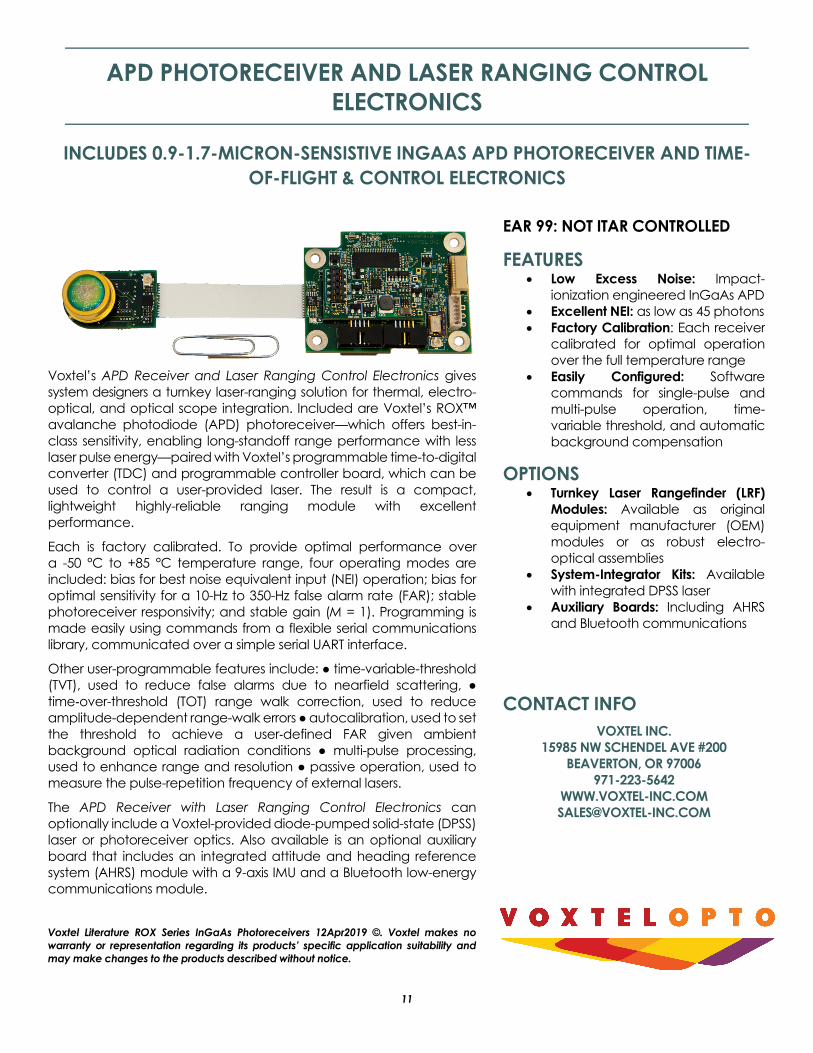
APD PHOTORECEIVER AND LASER RANGING CONTROL ELECTRONICS
INCLUDES 0.9-1.7-MICRON-SENSISTIVE INGAAS APD PHOTORECEIVER AND TIME-OF-FLIGHT & CONTROL ELECTRONICS
Voxtel’s APD Receiver and Laser Ranging Control Electronics gives system designers a turnkey laser-ranging solution for thermal, electro-optical, and optical scope integration. Included are Voxtel’s ROX™ avalanche photodiode (APD) photoreceiver—which offers best-in-class sensitivity, enabling long-standoff range performance with less laser pulse energy—paired with Voxtel’s programmable time-to-digital converter (TDC) and programmable controller board, which can be used to control a user-provided laser. The result is a compact, lightweight highly-reliable ranging module with excellent performance.
Each is factory calibrated. To provide optimal performance over a -50 °C to +85 °C temperature range, four operating modes are included: bias for best noise equivalent input (NEI) operation; bias for optimal sensitivity for a 10-Hz to 350-Hz false alarm rate (FAR); stable photoreceiver responsivity; and stable gain (M = 1). Programming is made easily using commands from a flexible serial communications library, communicated over a simple serial UART interface.
Other user-programmable features include: time-variable-threshold (TVT), used to reduce false alarms due to nearfield scattering, time-over-threshold (TOT) range walk correction, used to reduce amplitude-dependent range-walk errors autocalibration, used to set the threshold to achieve a user-defined FAR given ambient background optical radiation conditions multi-pulse processing, used to enhance range and resolution passive operation, used to measure the pulse-repetition frequency of external lasers.
The APD Receiver with Laser Ranging Control Electronics can optionally include a Voxtel-provided diode-pumped solid-state (DPSS) laser or photoreceiver optics. Also available is an optional auxiliary board that includes an integrated attitude and heading reference system (AHRS) module with a 9-axis IMU and a Bluetooth low-energy communications module.
Voxtel Literature ROX Series InGaAs Photoreceivers 12Apr2019 ©. Voxtel makes no warranty or representation regarding its products’ specific application suitability and may make changes to the products described without notice.
EAR 99: NOT ITAR CONTROLLED
FEATURES Low Excess Noise: Impact-
ionization engineered InGaAs APD Excellent NEI: as low as 45 photons Factory Calibration: Each receiver
calibrated for optimal operation over the full temperature range
Easily Configured: Software commands for single-pulse and multi-pulse operation, time-variable threshold, and automatic background compensation
OPTIONS Turnkey Laser Rangefinder (LRF)
Modules: Available as original equipment manufacturer (OEM) modules or as robust electro-optical assemblies
System-Integrator Kits: Available with integrated DPSS laser
Auxiliary Boards: Including AHRS and Bluetooth communications
CONTACT INFO VOXTEL INC.
15985 NW SCHENDEL AVE #200 BEAVERTON, OR 97006
971-223-5642 WWW.VOXTEL-INC.COM [email protected]
12
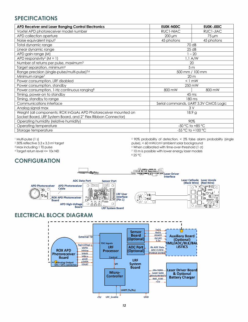
SPECIFICATIONS
APD Receiver and Laser Ranging Control Electronics EU0K-N00C EU0K-J00C Voxtel APD photoreceiver model number RUC1-NIAC RUC1-JIAC APD collection aperture 200 µm 75 µm Noise equivalent input1 45 photons 45 photons Total dynamic range 70 dB Linear dynamic range 25 dB APD gain range (M) 1 – 20 APD responsivity2 (M = 1) 1.1 A/W Number of returns per pulse, maximum3 20 Target separation, minimum4 5 m Range precision (single-pulse/multi-pulse)5,6 500 mm / 100 mm Minimum range7 20 m Power consumption, LRF disabled < 1 mW Power consumption, standby 250 mW Power consumption, 1-Hz continuous ranging8 800 mW 800 mW Timing, power-on to standby 45 ms Timing, standby to range 180 ms Communications interface Serial commands, UART 3.3V CMOS Logic Analog signal max 3 V Weight (all components: ROX InGaAs APD Photoreceiver mounted on Socket Board, LRF System Board, and 2” Flex Ribbon Connector)
18.9 g
Operating humidity (relative humidity) 90% Operating temperature -50 °C to +85 °C Storage temperature -55 °C to +100 °C
1 Multi-pulse (1 s) 2 30% reflective 3.3 x 3.3 m2 target 3 Max including 1 T0 pulse 4 Target return level <= 10x NEI
5 90% probability of detection, < 2% false alarm probability (single pulse), < 60 mW/cm2 ambient solar background 6 When calibrated with time-over-threshold (1 σ) 7 10 m is possible with lower energy laser models 8 25 °C
CONFIGURATION
ELECTRICAL BLOCK DIAGRAM

13
Connector Pin Assignments
LRF System Board User Interface (Hirose DF3-8P-2DS)
APD Photoreceiver Board The functionality of the electrical connections to the APD photoreceiver can be found on the ROX InGaAs APD Photoreceivers datasheet and user manual.
Pin Name In/Out Description Typ 1 VAPD Input APD bias voltage 2 GND Input Ground GND 3 NC Input High voltage isolation NA 4 GND Input Ground 5 AGND Input Analog ground GND 6 SIG- Output 1.8V full-swing complementary digital output signal from receiver 1.8V 7 AGND Input Analog ground 8 SIG+ Output 1.8V full-swing complementary digital output signal from receiver 1.8V 9 3.3V Input 3.3V digital supply 3.3V 10 GND Input Ground 11 VthSW Input Threshold voltage switch for TVT—switches between VTh,hi and Vth, lo 12 NC NA No connect NA 13 VthL Input Threshold low voltage 14 GND Input Ground GND 15 VthH Input Threshold high voltage 16 uCLK Input i2c clock for photoreceiver (two-wire interface) 17 AGND Input Analog ground 18 uDATA Input i2c data for photoreceiver (two-wire interface) 19 VCMOS2 Input 5V ROX photoreceiver supply 5VDC 20 START Input Receiver mode control
UFL Connector Analog Output Analog Output 1.8 V
Laser Driver Board For electrical connections to the laser driver board, see Voxtel’s DPSS Laser datasheet.
Pin Name In/Out Description Min Typ Max
1 LRF_RANGE Input Initiates a range measurement when a rising edge is detected on this pin.
3.3 V
2 LASERGATE Output Laser gate signal to the laser diode driver board. This can be monitored or actively driven.
3.3 V
3 LRF_ENABLE Input Active low enable. Pin pulled up to 5V with 100 kΩ resistor.
Pull low to enable LRF power.
4 NC NA No Connect NA 5 GND Input System Ground Ground 6 TX Output UART Transmit 3.3V 7 RX Input UART Receiver 3.3V 8 5V Input System Power Input 5V
14
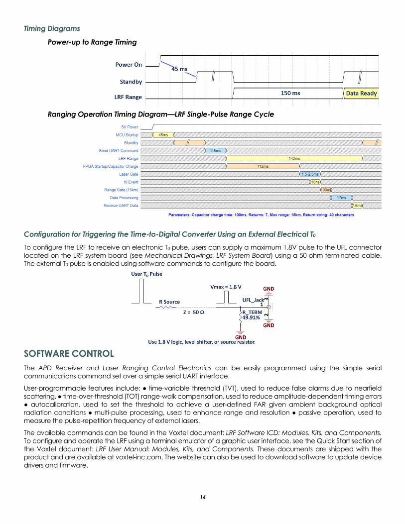
Timing Diagrams
Power-up to Range Timing
Ranging Operation Timing Diagram—LRF Single-Pulse Range Cycle
Configuration for Triggering the Time-to-Digital Converter Using an External Electrical T0 To configure the LRF to receive an electronic T0 pulse, users can supply a maximum 1.8V pulse to the UFL connector located on the LRF system board (see Mechanical Drawings, LRF System Board) using a 50-ohm terminated cable. The external T0 pulse is enabled using software commands to configure the board.
SOFTWARE CONTROL The APD Receiver and Laser Ranging Control Electronics can be easily programmed using the simple serial communications command set over a simple serial UART interface.
User-programmable features include: time-variable threshold (TVT), used to reduce false alarms due to nearfield scattering, time-over-threshold (TOT) range-walk compensation, used to reduce amplitude-dependent timing errors autocalibration, used to set the threshold to achieve a user-defined FAR given ambient background optical radiation conditions multi-pulse processing, used to enhance range and resolution passive operation, used to measure the pulse-repetition frequency of external lasers.
The available commands can be found in the Voxtel document: LRF Software ICD: Modules, Kits, and Components. To configure and operate the LRF using a terminal emulator of a graphic user interface, see the Quick Start section of the Voxtel document: LRF User Manual: Modules, Kits, and Components. These documents are shipped with the product and are available at voxtel-inc.com. The website can also be used to download software to update device drivers and firmware.
15
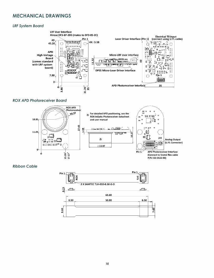
MECHANICAL DRAWINGS
LRF System Board
ROX APD Photoreceiver Board
Ribbon Cable
16
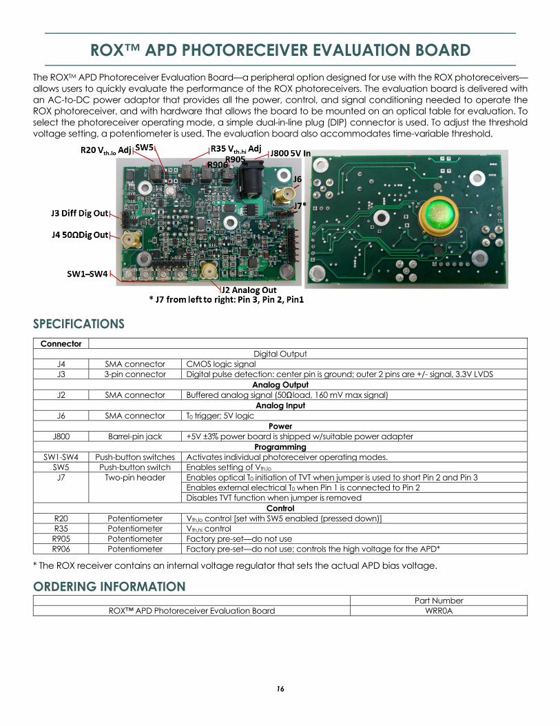
ROX™ APD PHOTORECEIVER EVALUATION BOARD The ROXTM APD Photoreceiver Evaluation Board—a peripheral option designed for use with the ROX photoreceivers—allows users to quickly evaluate the performance of the ROX photoreceivers. The evaluation board is delivered with an AC-to-DC power adaptor that provides all the power, control, and signal conditioning needed to operate the ROX photoreceiver, and with hardware that allows the board to be mounted on an optical table for evaluation. To select the photoreceiver operating mode, a simple dual-in-line plug (DIP) connector is used. To adjust the threshold voltage setting, a potentiometer is used. The evaluation board also accommodates time-variable threshold.
SPECIFICATIONS Connector
Digital Output J4 SMA connector CMOS logic signal J3 3-pin connector Digital pulse detection: center pin is ground; outer 2 pins are +/- signal, 3.3V LVDS
Analog Output J2 SMA connector Buffered analog signal (50Ωload, 160 mV max signal)
Analog Input J6 SMA connector T0 trigger; 5V logic
Power J800 Barrel-pin jack +5V ±3% power board is shipped w/suitable power adapter
Programming SW1-SW4 Push-button switches Activates individual photoreceiver operating modes.
SW5 Push-button switch Enables setting of Vth,lo J7 Two-pin header Enables optical T0 initiation of TVT when jumper is used to short Pin 2 and Pin 3
Enables external electrical T0 when Pin 1 is connected to Pin 2 Disables TVT function when jumper is removed
Control R20 Potentiometer Vth,lo control [set with SW5 enabled (pressed down)] R35 Potentiometer Vth,hi control R905 Potentiometer Factory pre-set—do not use R906 Potentiometer Factory pre-set—do not use; controls the high voltage for the APD*
* The ROX receiver contains an internal voltage regulator that sets the actual APD bias voltage.
ORDERING INFORMATION Part Number
ROX™ APD Photoreceiver Evaluation Board WRR0A