roughness effects on the electrical conductivity of thin films grown in a quasi-layer-by-layer mode
TRANSCRIPT

erlands
PHYSICAL REVIEW B, VOLUME 63, 125404
Roughness effects on the electrical conductivity of thin films grown in a quasi-layer-by-layer mode
G. Palasantzas* and J. Th. M. De HossonDepartment of Applied Physics, Materials Science Center, University of Groningen, Nijenborgh 4, 9747 AG Groningen, The Neth
~Received 12 July 2000; revised manuscript received 18 October 2000; published 12 March 2001!
We investigate morphology effects on the electrical conductivity on thin semiconducting and metallic filmsgrown in a quasi-layer-by-layer growth mode within the framework of quantum-mechanical electron transporttheory. The film growth mode is described by a nonequilibrium Sine–Gordon model that incorporatesevaporation/recondensation, surface diffusion, and lattice pinning effects. For semiconducting films, pinningeffects manifest themselves as oscillations superimposed on a smoothly increasing conductivity with growthtime. For metallic films, quantum size effect oscillations are strongly convoluted with pinning induced oscil-lations, which dominate the conductivity variations at later stages of growth.
DOI: 10.1103/PhysRevB.63.125404 PACS number~s!: 73.50.2h, 72.10.Fk, 73.50.Dn
ssie
pesrre
ec
i-eoi
foaa
veIn
ye
o
–
rs
te
Lscm
hhiny-ouic
se-
nn
ing.
c-n
-
e
k-
c-n-
umn-
I. INTRODUCTION
Deviations of thin film surfaces/interfaces from flatnehave strong influence on their electrical transport propertsince they induce additional electron scattering.1–7 Electronscattering by random roughness alters the size and shaquantum size effects~QSE! in a manner that dependstrongly on the form of the corresponding roughness colation function associated with the nature of roughnessshort and long roughness wavelengths.3,5 In addition, the filmgrowth mode as well as cross-correlation roughness effcan also strongly influence the conductivity of thin films.7
At any rate, a layer-by-layer growth mode would elimnate additional electron scattering due to surface roughnIndeed, at high temperature molecular beam epitaxyatomic layer epitaxy, the growth in a layer-by-layer modeanticipated where each depositing layer is completed bethe growth of the next layer starts.6,8 Nevertheless, suchgrowth mode does not always takes place. Instead, a qulayer-by-layer is expected where some nucleation on topalready existing islands can commence, which is, howeonly a small portion compared to the bottom grown layer.systems where layer-by-layer growth or quasi-layer-by-lagrowth6,8 commences, QSE oscillations have been shownbe altered by surface/interface roughness convoluted bycillations imposed by morphology characteristics.7
For example, conductivity measurements in Pb and Pballoyed films grown on Si~111!636-Au and Au films onSi~111!737,6 where quasi-layer-by-layer growth occushowed oscillations with 1 ML~monolayer! period associ-ated with periodic changes in roughness, and were consiswith reflection high energy electron diffraction~RHEED!measurement. Moreover, an additional oscillation of 2 Mperiod was observed which was associated with QSE olations. In addition, oscillations in resistivity versus filthickness have been observed in Pt films,9 and Ag, In, Gafilms grown on thick Ag and Au basis layers.10
In this paper, we perform a theoretical investigation of tquasi-layer-by-layer grown morphological effects on the tfilm conductivity convoluted with QSE. The quasi-layer-blayer mode will be described in terms of a Sine–Gord~SG! model that incorporates both surface relaxation by sface diffusion and/or evaporation/recondensation. Compl
0163-1829/2001/63~12!/125404~6!/$15.00 63 1254
s,
of
-at
ts
ss.r
sre
si-ofr,
rtos-
In
nt
-il-
e
nr-a-
tions of convolution of QSE and morphology oscillationwill be investigated thoroughly for semiconducting and mtallic films through a quantum-mechanical Boltzmaapproach3–5 that allows calculation of thin film conductivityinfluenced solely by electron boundary roughness scatter
II. CONDUCTIVITY THEORYAND QUASI-LAYER-BY-LAYER GROWTH MODEL
Conductivity formalism
In the Born approximation, the in-plane electrical condutivity of thin films bounded solely by roughness electroscattering is given by3,5
s5e2\3
m2^h& (n51
N
(n851
N
qn2qn8
2@C21#nn8 , ~1!
Cnn8~EF!5E0
2pH dnnAnkn2 (
m51
N
Am^uh~qnm ,t !u2&
2AnAn8^uh~qnn8 ,t !u2&cosuJ du, ~2!
whereqnn85(qn21qn8
222qnqn8 cosu)1/2, qn5@(2m/\2)(EF
2En)#1/2 with EF andEn being, respectively, the Fermi energy and the energy minimum of then miniband edge, andAn5uFn(^h&/2)u2 with Fn(z) the quantized electron wavfunction along thez axis for a flat film.N is the number ofelectron populated lateral subbands andh(q,t) the surfaceroughness fluctuation from flatness. For a flat film of thicness^h& and carrier densityn, EF , andN are determined bythe condition5 n^h&5(m/p\2)(NEF→(n51,NEn) with ns5n^h& the areal electron density. If, for simplicity, the eletrons are localized in the film by an infinite confining potetial well, then An5\2p2n2/m^h&3 and En5(\2/2m)(np/^h&)2.3,5 Clearly the knowledge of the roughness spectr^uh(q,t)u2& is required to further calculate the electron coductivity from Eqs.~1! and ~2!.
©2001 The American Physical Society04-1
hequ
-
ge
thto
r ow
faDswt
y
c-
tio(
s
-ngtion
r
r-
ity
G. PALASANTZAS AND J. TH. M. DE HOSSON PHYSICAL REVIEW B63 125404
Growth model
A quasi-layer-by-layer growth can be described by a pnomenological Langevin equation representing the nonelibrium analogue of the SG model11–13
]h~r ,t !
]t5R1n¹2h2k¹4h1h~r ,t !2A sinF2ph~r ,t !
c G ,~3!
with h(r ,t) the surface height,R the rate of impinging adatoms,n the evaporation/recondensation coefficient, andk thediffusion coefficient. h(r ,t) represents intrinsic randomnoise fluctuations of amplitude D such that^h(r ,t)h(r 8,t8)&52Dd(r2r 8)d(t2t8) and ^h(r ,t)&50which are responsible for roughening during growth.A is thestrength of the pinning term that favors energetically intevalues of surface heights in units of the atomic spacingc.11,13
Indeed, the pinning forceVpin52A sin@2ph(r ,t)/c# mim-ics qualitatively two-dimensional~2D! nucleation-dominatedgrowth process. For low surface coverage, such thatVpin,0, there are a few atoms on the top layer and thuspossibility of 2D islands to overcome the potential barrierreach the critical island size is small. As a result a numbedeposited atoms that are not stable on the crystal surfaceevaporate back into the vapor phase. With increasing surcoverage such thatVpin.0, on the surface there are many 2islands leading to an enhanced probability that monomerbe attached to islands resulting in an easier groprocess.12,13 For a small pinning force Vpin52«A sin@2ph(r ,t)/c#, Eq.~3! can be solved perturbativeland the roughness spectrum^uh(q,t)u2& is given by~see Ap-pendix!
^uh~q,t !u2&5D12e22~kq41nq2!t
kq41nq2
1ADc
pR
e22~kq41nq2!t
kq41nq2 sin~2pRt/c!
24ADcos~2pRt/c!2e22~kq41nq2!t
~2pR/c!214~kq41nq2!2
24AD
c~kq41nq2!
sin~2pRt/c!
~2pR/c!214~kq41nq2!2 ,
~4!
which is what is required in the calculation of the film eletrical conductivity.3
III. RESULTS AND DISCUSSION
Our conductivity calculations~unless stated! were per-formed for growth rateR53 Å/s, D50.2 Å/s, and c53 Å, as well as the units of the coefficientsn and k areassumed such that@n#5Å 2/s and @k#5Å 4/s. In addition,we note that the contribution of evaporation/recondensain surface relaxation is significant at larger length scalesr.2pAk/n), while the shorter length scales (r ,2pAk/n)surface diffusion is the dominant one.
12540
-i-
r
e
fillce
toh
n
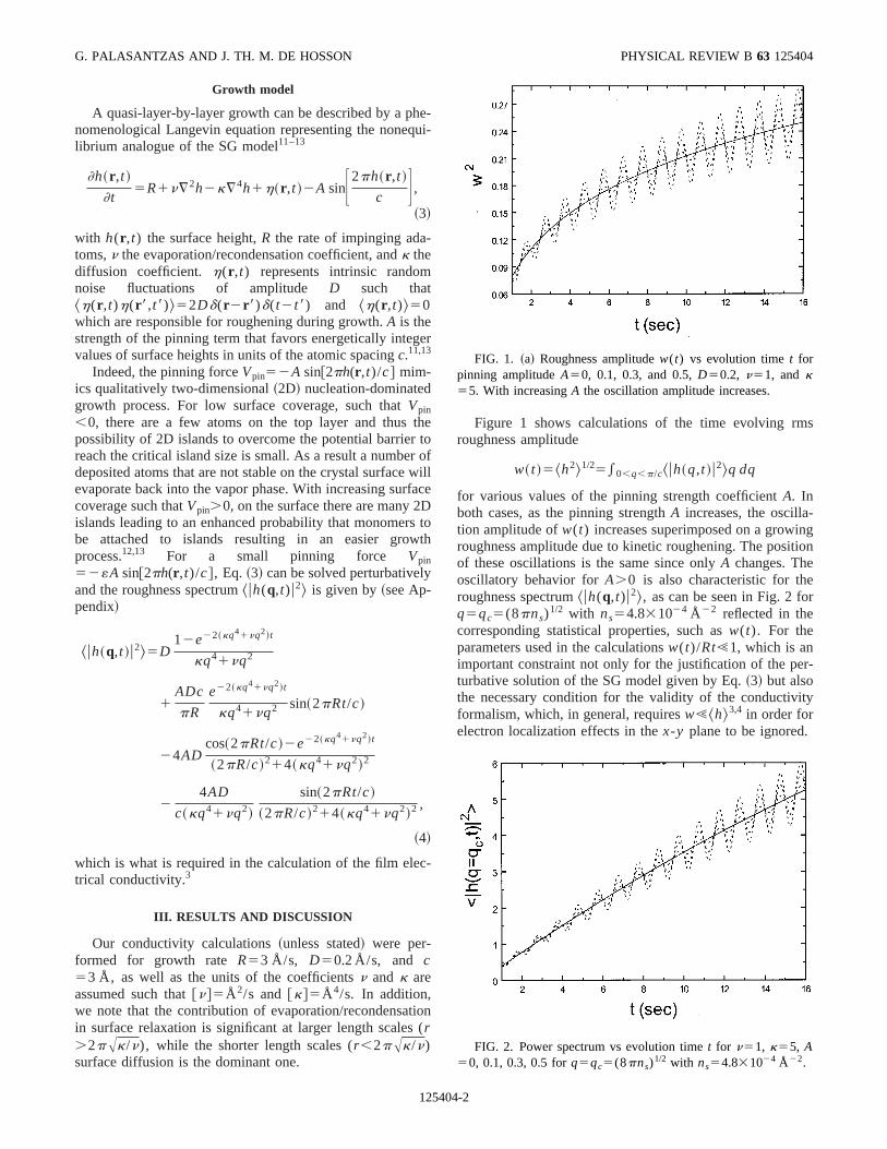
Figure 1 shows calculations of the time evolving rmroughness amplitude
w~ t !5^h2&1/25*0,q,p/c^uh~q,t !u2&q dq
for various values of the pinning strength coefficientA. Inboth cases, as the pinning strengthA increases, the oscillation amplitude ofw(t) increases superimposed on a growiroughness amplitude due to kinetic roughening. The posiof these oscillations is the same since onlyA changes. Theoscillatory behavior forA.0 is also characteristic for theroughness spectrumuh(q,t)u2&, as can be seen in Fig. 2 foq5qc5(8pns)
1/2 with ns54.831024 Å 22 reflected in thecorresponding statistical properties, such asw(t). For theparameters used in the calculationsw(t)/Rt!1, which is animportant constraint not only for the justification of the peturbative solution of the SG model given by Eq.~3! but alsothe necessary condition for the validity of the conductivformalism, which, in general, requiresw!^h&3,4 in order forelectron localization effects in thex-y plane to be ignored.
FIG. 1. ~a! Roughness amplitudew(t) vs evolution timet forpinning amplitudeA50, 0.1, 0.3, and 0.5,D50.2, n51, andk55. With increasingA the oscillation amplitude increases.
FIG. 2. Power spectrum vs evolution timet for n51, k55, A50, 0.1, 0.3, 0.5 forq5qc5(8pns)
1/2 with ns54.831024 Å 22.
4-2

bet
s-rfaemsth
ghfe
ecavg
ao
annn
ortsg
u
u-th,a
m
n inforonn-
ofentrete-m-
ofor
he
attiv-
for
ateibu-in-ig-
it
ROUGHNESS EFFECTS ON THE ELECTRICAL . . . PHYSICAL REVIEW B 63 125404
Nevertheless, we should point out that the oscillatoryhavior is smaller at the early stages of growth. This is duethe fact that Eq.~1! is a continuous model. As a result, dicrete lattice effects are ignored. Indeed, as long as the sucoverageu$5^h&2 in@^h&/c#c% is not an integer, the surfacwill be rough independent of the smoothing mechanisSuch a process is highly washed out at very early stagegrowth. Such an effect can be corrected by consideringfact that the 2D-nucleation growth mode and dynamic rouening are independent, which allows to consider as an eftive interface widthw[Aw21wdis
2 with wdis2 5cu(12u).
Figure 3 shows the influence of the discrete lattice effcorrection, which leads to recovery of the oscillatory behior at early growth stages. At later growth stages, the Lanvin equation dominates the description of roughening13 al-lowing its use for electron transport calculations.
Semiconducting film conductivity
When the number of occupied lateral minibands is sm~e.g., N51,2), the film is termed as semiconducting. Fonly one lateral miniband populated (N51) there are noquantum size effects present. In this case, only intraminibscattering contributes to the conductivity simplifying the uderstanding of pinning effects on the conductivity depedence with increasing growth time. As a result, an oscillatbehavior present will arise solely from morphology effecassociated in the present case to pinning effects favorinlayer-by-layer growth.
Figure 4 shows the temporal dependence of the condtivity for sufficiently low areal electron densityns54.831024 Å 22 in such a way that only one miniband is poplated for the thicknesses or growth times considered. Inabsence of a pinning force,A50, as shown by the solid linethe conductivity increases with growth time followingsimple power law behaviors}tX with X5X(n,k) and de-pending on the strength of the relaxation mechanis
FIG. 3. Roughness amplitudew vs evolution timet with andwithout discrete lattice effect correction forA50.2, D50.5, R53, c53, k52, n50 ~diffusion dominated surface relaxation!.The roughness amplitude increases almost linearly with time wan oscillating growth rate of small amplitude sinceR@A.
12540
-o
ce
.ofe-c-
t-e-
llr
d--y
a
c-
e
s,
namely evaporation/recondensation and surface diffusiothe present case. However, as pinning starts to contributeA.0, additional oscillations occur and are superimposedthe conductivity increment that occurs in an oscillatory maner. With increasing pinning strengthA, the conductivity os-cillation amplitude increases especially at latter stagesgrowth. Nevertheless, the existence of the initial transiregime, where the continuum equation washes out disclattice effects~see Fig. 3!, is also pronounced for the conductivity besides that of morphological roughness paraeters such as the rms roughness amplitudew ~Fig. 1!.
In order to gain further understanding on the effectpinning on the conductivity, we consider the following. Fone miniband occupied (N51), the conductivity is givenby5
s52nse
2
\p3 ^h&5F E0
2p
^uh~q11,t !u2&~12cosu!duG21
~5!
with q115@4pns(12cosu)#1/2 for an infinite potential well.5
Equation~5! shows that the spatial frequency regime of tmorphology with wave vectors 0,q,qc5(8pns)
1/2 willcontribute to the film conductivity. This is due to the fact thforward scattering, which contributes less to the conducity, occurs foru50 or 2p yielding q1150, while backwardscattering has the largest contribution to the conductivityu5p yielding q115qc5(8pns)
1/2. For forward scatteringthe integrand in the integral part of Eq.~5! becomes
limu→0,2p^uh~q11,t !u2&~12cosu!
5@~ADc/pR!2~ADc/p2R2!#sin~2pRt/c!
which has a positive amplitude @(ADc/pR)2(ADc/p2R2)#&.0 for R.1/p. For backward scatteringwe obtain ^uh(q115qc ,t)u2&(12cosp)52^uh(q115qc ,t)u2&which is always positive independently of the deposition rR. Therefore, depending on the deposition rate, the contrtion of backward and forward scattering on the pinningduced morphological oscillations could be in-phase for s
h
FIG. 4. Conductivitys vs evolution timet for semiconductingfilms with areal electronns54.831024 Å 22, D50.2, n51,k55, andA50 ~solid line!, 0.1, 0.3, 0.5.
4-3

-initythetyec
in-(llath
thivielo
ofteen
ncth
rtsthr
-pimsodr-
ted
arsrip-see ofthethens
g totionwensin-ol-
G. PALASANTZAS AND J. TH. M. DE HOSSON PHYSICAL REVIEW B63 125404
nificant deposition ratesR.1/p or out-of-phase for very lowdeposition rates, such thatR,1/p. Figure 2 shows the behavior of the roughness spectrum for backward scatterwhich has the strongest contribution to the conductivClearly it can be seen that at the early stages of growth,morphological oscillations arising from pinning are rathweak, thus implying a weak contribution to the conductiviand vice versa upon inclusion of the discrete lattice effcorrection, which is depicted in Fig. 3.
Metallic film conductivity
For metallic films the number of occupied minibandscreases rapidly with increasing thickness or growth timeN@1), leading alternatively to the presence of QSE oscitions. These oscillations arise from the fact that each timeFermi level crosses the bottom of a lateral miniband anochannel for scattering opens, which reduces the conductand further leads to an oscillatory increment. In general, thshape and size depends on the particular rough morphounder consideration as previous studies have shown.3,5,7 Thesituation for metallic films is more complex than thatsemiconducting films; since besides intraminiband scating, transitions between lateral minibands leading to intminiband scattering yield significant contributions the coductivity behavior@cross-terms in Eq.~2!#.
As can be seen in Fig. 4 by the solid line, in the abseof pinning or A50, the QSE oscillations have a saw-toostructure with increasing growth time and a period;lF/2with lF the Fermi wavelength. As long as pinning stacontributing to conductivity, the shape and magnitude ofoscillations start to deviate from the pure QSE oscillatobehavior ~absence of pinning;A50), and rather interpenetrate through these pure QSE oscillations. The effect ofning, in comparison to the case of semiconducting filshown in Fig. 5, starts to appear even at very early stagegrowth and progressively prevails over the pure QSE mwith increasing growth time. In addition, with increasing su
FIG. 5. Conductivitys vs evolution timet for metallic filmswith bulk electron densityn513.231022 Å 23, D50.2, n51, k55, andA50 ~solid line!, 0.1, 0.3, 0.5.
12540
g,.e
r,t
-e
ertyirgy
r-r--
e
ey
n-sofe
face relaxation~increasing coefficientv and/ork! the ampli-tude of pinning induced oscillations increases, as is depicin Fig. 6.
At later growth stages where the effect of pinning appeto be more pronounced within the continuum model desction, the conductivity oscillations bear similarities with thoof the semiconducting case indicating a strong dominancmorphological effects over quantum effects arising fromelectron confinement in the direction perpendicular tofilm surface. In Fig. 7 we present conductivity calculatiofor various bulk electron densities in the rangen513.231024– 13.231022 Å 23. With lower electron density thenumber of populated lateral minibands decreases leadinless QSE oscillations, and as a result, to reduced contribuof inter-miniband scattering. Comparing Figs. 5 and 7,can infer that in the latter case, pinning induced oscillatioare more affected by QSE oscillations complicating theterpretation of the conductivity behavior altered by morphogy effects.
FIG. 6. Conductivitys vs evolution timet for metallic filmswith bulk electron densityn513.231022 Å 23, D50.2, n5k50.1, 0.5, 1, andA50.2.
FIG. 7. Conductivitys vs evolution timet for metallic filmswith various bulk electron densities, as indicated forR53, c53,A50.2, k55, andv52.
4-4

thllicinro
ioo
inh.mrmei
ema
hee
atio
atngs
um
ro
sto
ea
ur-ba-.
ROUGHNESS EFFECTS ON THE ELECTRICAL . . . PHYSICAL REVIEW B 63 125404
IV. CONCLUSIONS
In conclusion, we investigated roughness effects onelectrical conductivity on thin semiconducting and metafilms grown in a quasi-layer-by-layer growth mode withthe framework of Boltzmann quantum-mechanical electtransport theory. The film growth mode was describedterms of a nonequilibrium Sine-Gordon model that incorprates roughening and surface relaxation in termsevaporation/recondensation and surface diffusion, combwith lattice pinning effects that favor layer-by-layer growtThe latter type of growth effect manifests itself on the teporal evolution of roughness parameters, such as theroughness amplitude. For semiconducting films, pinningfects manifest themselves as oscillations on an otherwsmoothly increasing conductivity with growth time in thabsence of pinning. However, for metallic films, quantusize effect oscillations are convoluted with morphologicoscillations leading to complex oscillatory patterns of tconductivity versus thickness or growth evolution timClearly for metallic films, pinning induced oscillationslater stages of growth dominate the conductivity behavover quantum mechanical induced oscillations~QSE!. At anyrate, we should point out that our results are limited to lstages of growth thus minimizing the effect of neglectidiscrete lattice effects~Fig. 3!. Further studies are in progresto properly incorporate discrete lattice effects in quantmechanical thin film conductivity calculations.
ACKNOWLEDGMENTS
We would like to acknowledge support from the Nethelands Institute for Metals Research, and important correspdence with Dr. Y.-P. Zhao from Renselaer Polytechnic Intute for communicating his calculations on pinning effectsrough growth fronts prior to publication,13 as well as provid-ing Fig. 3 to illustrate discrete lattice effects. Moreover, wwould like to acknowledge useful discussions with J. Barn
APPENDIX
If we assume the perturbative expansionh5h11«h21«2h31 . . . , Eq.~3! yields
]h1
]t5R1n¹2h12k¹4h11n;
]h2
]t5n¹2h22k¹4h22A sinS 2ph1
c D1n. ~A1!
By settingh15h1,01h1,1 with h1,05Rt, we obtain from Eq.~A1!
12540
e
nn-f
ed
-s
f-se
l
.
r
e
-n-i-n
s.
h1,1~q,t !5E0
t
n~q,t!e2~kq41nq2!~ t2t!dt ~A2!
with h1,0 andh1,1 representing, respectively, the average sface height and the height fluctuation at zero-order perturtion. Since usuallyh1,1
2 &!h1,0, the pinning-sine term in Eq~A1! can be further approximated by
]h2
]t5n¹2h22k¹4h22A sinS 2pR
ct D
22pA
ch1,1cosS 2pR
ct D . ~A3!
Therefore, if we seth25h2,01h2,1 such that
]h2,0
]t52A sinS 2pR
ct D ,
]h2,1
]t5n¹2h2,12k¹4h2,1
22pA
ch1,1cosS 2pR
ct D ~A4!
and integrate, we obtain the average film thickness^h&5h1,01h2,0
^h&5Rt1Ac
2pR FcosS 2pR
ct D21G ~A5!
and
h2,1~q,t !52AE0
t
h1,1~q,t!cos~2pRt/c!e2~kq41nq2!~ t2t!dt,
~A6!
which finally yields the roughness spectrum of Eq.~4!.
s,
*Corresponding author. Electronic mail:[email protected]
1T. Ando, A. B. Fowler, and F. Stern, Rev. Mod. Phys.54, 437~1982!; A. Hartstein, T. H. Ning, and A. B. Fowler, Surf. Sci.58, 178 ~1976!; T. Ando, Jpn. J. Phys.51, 3900~1982!.
2J. C. Hensel, R. T. Tung, J. M. Poate, and F. C. Unterwald, Phy
4
.
Rev. Lett. 54, 1840 ~1985!; P. A. Badoz, A. Briggs, E.Rosencher, A. A. d’ Avitaya, and C. d’Anterroches, Appl. Phys.Lett. 51, 169 ~1985!; J. Y. Duboz, P. A. Badoz, E. Rochencher,J. Henz, M. Ospelt, H. von Kanel, and A. A. Briggs,ibid. 53,788 ~1988!; R. G. P. van der Kraan, J. F. Jongste, H. M. LaegerG. c. A. M. Janssen, and S. Radelaar, Phys. Rev. B44, 13 140
-5

ue
r,,
M.
s
Ap-ol.
G. PALASANTZAS AND J. TH. M. DE HOSSON PHYSICAL REVIEW B63 125404
~1991!.3G. Fishman and D. Calecki, Phys. Rev. Lett.62, 1302~1989!; G.
Fishman and D. Calecki, Phys. Rev. B43, 11 581 ~1991!; J.Barnas and Y. Bruynseraede, Europhys. Lett.32, 167 ~1995!; J.Barnas and Y. Bruynseraede, Phys. Rev. B53, 5449~1996!.
4H. Sakaki, T. Noda, K. Hirakawa, M. Tanaka, and T. MatsusAppl. Phys. Lett.51, 1934 ~1987!; A. Gold, Z. Phys. B: Con-dens. Matter74, 2100~1989!.
5G. Palasantzas and J. Barnas, Phys. Rev. B56, 7726 ~1997!; G.Palasantzas and J. Barnas, Phys. Status Solidi B209 , 319~1998!; J. Barnas and G. Palasntzas, J. Appl. Phys.82, 3950~1997!.
6M. Jolocowvski and E. Bauer, Phys. Rev. B38, 5272~1988!; M.Jolocowvski, E. Bauer, H. Knoppe, and G. Lilienkamp,ibid. 45,13 607 ~1992!; M. Jolocowvski, M. Hoffmann, and E. BauePhys. Rev. Lett.76, 4227~1996!; M. Jolocowvski and E. BauerPhys. Rev. B37, 8622~1988!.
12540
,
7G. Palasantzas, Y.-P. Zhao, G.-C. Wang, T.-M. Lu, and J. Th.De Hosson, Phys. Rev. B61, 11 109~2000!.
8F. Rosenberger, inInterfacial Aspects of Phase Transformation,edited by B. Mutaftschiev~Reidel, Dordrecht, 1982!.
9G. Fischer and H. Hoffmann, Z. Phys. B39, 287 ~1980!; H.Hoffmann and G. Fischer, Thin Solid Films36, 25 ~1976!.
10D. Schumacher and D. Stark, Surf. Sci.123, 384 ~1982!.11H.-Y. Yang, G.-C. Wang, and T.-M. Lu, Phys. Rev. B51, 17 932
~1995!.12P. Nozieres, inSolid Far From Equilibrium, edited by C.
Godrche~Cambridge University Press, New York, 1991!, pp.135–143.
13Y. P. Zhao, G.-C. Wang, and T.-M. Lu,Characterization ofAmorphous and Crystalline Rough Surfaces-Principles andplications, Experimental Methods in the Physical Science V37 ~Academic Press, New York, 2000!.
4-6