root cause analysis and classification of single point
TRANSCRIPT
Brigham Young University Brigham Young University
BYU ScholarsArchive BYU ScholarsArchive
Theses and Dissertations
2020-12-15
Root Cause Analysis and Classification of Single Point Failures in Root Cause Analysis and Classification of Single Point Failures in
Designs Applying Triple Modular Redundancy in SRAM FPGAs Designs Applying Triple Modular Redundancy in SRAM FPGAs
James D. Swift Brigham Young University
Follow this and additional works at: https://scholarsarchive.byu.edu/etd
Part of the Engineering Commons
BYU ScholarsArchive Citation BYU ScholarsArchive Citation Swift, James D., "Root Cause Analysis and Classification of Single Point Failures in Designs Applying Triple Modular Redundancy in SRAM FPGAs" (2020). Theses and Dissertations. 8766. https://scholarsarchive.byu.edu/etd/8766
This Thesis is brought to you for free and open access by BYU ScholarsArchive. It has been accepted for inclusion in Theses and Dissertations by an authorized administrator of BYU ScholarsArchive. For more information, please contact [email protected], [email protected].
Root Cause Analysis and Classification of Single Point Failures in Designs Applying Triple
Modular Redundancy in SRAM FPGAs
James D. Swift
A thesis submitted to the faculty of
Brigham Young University
in partial fulfillment of the requirements for the degree of
Master of Science
Michael Wirthin-Chair, Chair
Brent Nelson
Brad Hutchings
Department of Electrical and Computer Engineering
Brigham Young University
Copyright © 2020 James D. Swift
All Rights Reserved
ABSTRACT
Root Cause Analysis and Classification of Single Point Failures in Designs Applying Triple
Modular Redundancy in SRAM FPGAs
James D. Swift
Department of Electrical and Computer Engineering, BYU
Master of Science
Radiation effects encountered in space or aviation environments can affect the configura-
tion bits in Field Programmable Gate Arrays (FPGA) causing errors in FPGA output. One method
of increasing FPGA reliability in radiation environments includes adding redundant logic to mask
errors and allow time for repair. Despite the redundancy added with triple modular redundancy
(TMR) and configuration scrubbing there exist some configuration bits that individually affect
multiple TMR domains causing errors in FPGA output. A new tool called DeBit is introduced
that identifies hardware resources associated with a single bit failure. This tool identifies a novel
failure mode involving global routing resources and the failure mode is verified through a series of
directed tests on global routing resources. Lastly, a mitigation strategy is proposed and tested on a
single error in a triple modular redundancy (TMR) design.
Keywords: single event upset, field programmable gate array, triple modular redundancy, reliabil-
ity, seu, fpga, tmr, James D. Swift, thesis

ACKNOWLEDGMENTS
I would like to thank my wife, Kjarstin Swift, for pushing me to finish this thesis, being
willing to listen and understand more about FPGAs than she ever wanted to know, and for the
endless comparisons with the intricacies of the piano. I never would have known how similar
pianos and FPGAs are without you.
I would like to thank Dr. Mike Wirthlin for his guidance and patience and for allowing me
to the freedom to discover despite the results taking longer than either of us expected. I would also
like to thank Dr. Brent Nelson for his ideas, thoughts, astounding character, and ability to listen
intently; I admire his calm, fatherly demeanor. I appreciate Andrew Keller, Hayden Rowberry,
and Tim Witting for brainstorming and sharing their ideas with me whenever I found myself at a
roadblock.
I would like the thank my parents, Scott and Claire Swift, for instilling my desire to attain
education. I would also like to thank my Johnson and Johnson managers (Bob Thistle, Sarah
Raymond, and Tom Gamache) for working with my schedule and giving me funds to fulfill my
masters despite looming deadlines.
This work was supported by the NSF Center for Space, High-Performance, and Resilient
Computing (SHREC), supported by the I/UCRC Program of the National Science Foundation un-
der Grant No. 1738550. The opinions, findings, and conclusions or recommendations expressed
are those of the author(s) and do not necessarily reflect the views of the National Science Founda-
tion.
TABLE OF CONTENTS
LIST OF TABLES . . . . . . . . . . . . . . . . . . . . . . . . . . . . . . . . . . . . . . . vi
LIST OF FIGURES . . . . . . . . . . . . . . . . . . . . . . . . . . . . . . . . . . . . . . vii
Chapter 1 Introduction . . . . . . . . . . . . . . . . . . . . . . . . . . . . . . . . . . . 1
Chapter 2 Background and Related Work . . . . . . . . . . . . . . . . . . . . . . . . 4
2.1 Radiation Errors . . . . . . . . . . . . . . . . . . . . . . . . . . . . . . . . . . . . 4
2.2 FPGA Radiation Errors . . . . . . . . . . . . . . . . . . . . . . . . . . . . . . . . 5
2.3 Single Event Upsets and Fault Injection . . . . . . . . . . . . . . . . . . . . . . . 6
2.4 Configuration Scrubbing . . . . . . . . . . . . . . . . . . . . . . . . . . . . . . . 7
2.5 Triple Modular Redundancy . . . . . . . . . . . . . . . . . . . . . . . . . . . . . 7
2.6 Triple Modular Redundancy in FPGAs . . . . . . . . . . . . . . . . . . . . . . . . 8
2.7 FPGA Root Cause Failure and Classification . . . . . . . . . . . . . . . . . . . . . 8
2.8 Thesis Contributions . . . . . . . . . . . . . . . . . . . . . . . . . . . . . . . . . 9
Chapter 3 Xilinx Series 7 Architecture . . . . . . . . . . . . . . . . . . . . . . . . . . 11
3.1 Clocking Region . . . . . . . . . . . . . . . . . . . . . . . . . . . . . . . . . . . 11
3.2 Tiles . . . . . . . . . . . . . . . . . . . . . . . . . . . . . . . . . . . . . . . . . . 12
3.3 Interconnect . . . . . . . . . . . . . . . . . . . . . . . . . . . . . . . . . . . . . . 14
3.4 Configurable Logic Blocks . . . . . . . . . . . . . . . . . . . . . . . . . . . . . . 15
3.5 Block Random Access Memory . . . . . . . . . . . . . . . . . . . . . . . . . . . 18
3.6 Digital Signal Processing . . . . . . . . . . . . . . . . . . . . . . . . . . . . . . . 19
3.7 Hard IP . . . . . . . . . . . . . . . . . . . . . . . . . . . . . . . . . . . . . . . . 19
3.8 Bitstream Configuration . . . . . . . . . . . . . . . . . . . . . . . . . . . . . . . . 21
3.9 Architecture Importance . . . . . . . . . . . . . . . . . . . . . . . . . . . . . . . 22
Chapter 4 DeBit: A Bit Analysis Tool . . . . . . . . . . . . . . . . . . . . . . . . . . . 23
4.1 DeBit: Bit Mapping . . . . . . . . . . . . . . . . . . . . . . . . . . . . . . . . . . 23
4.2 Bit Mapping-PIPs . . . . . . . . . . . . . . . . . . . . . . . . . . . . . . . . . . . 24
4.3 Bit Mapping-LUTs . . . . . . . . . . . . . . . . . . . . . . . . . . . . . . . . . . 26
4.4 DeBit: Bit Analysis . . . . . . . . . . . . . . . . . . . . . . . . . . . . . . . . . . 27
4.5 Routing and Clock Bit Errors . . . . . . . . . . . . . . . . . . . . . . . . . . . . . 28
4.6 LUT Bit Errors . . . . . . . . . . . . . . . . . . . . . . . . . . . . . . . . . . . . 28
4.7 Slice Site Bit Errors . . . . . . . . . . . . . . . . . . . . . . . . . . . . . . . . . . 29
4.8 ECC Bit Errors . . . . . . . . . . . . . . . . . . . . . . . . . . . . . . . . . . . . 29
4.9 Unknown Bit Errors . . . . . . . . . . . . . . . . . . . . . . . . . . . . . . . . . . 30
4.10 Verifying DeBit . . . . . . . . . . . . . . . . . . . . . . . . . . . . . . . . . . . . 30
Chapter 5 SEU Root Cause Analysis . . . . . . . . . . . . . . . . . . . . . . . . . . . 31
5.1 TMR SEU Analysis . . . . . . . . . . . . . . . . . . . . . . . . . . . . . . . . . . 31
5.2 PIP Junction Analysis . . . . . . . . . . . . . . . . . . . . . . . . . . . . . . . . . 32
iv
5.3 PIP Junction Analysis: Regular Nets . . . . . . . . . . . . . . . . . . . . . . . . . 33
5.4 PIP Junction Analysis: Global Nets . . . . . . . . . . . . . . . . . . . . . . . . . . 35
5.5 PIP Junction Analysis: Application to TMR . . . . . . . . . . . . . . . . . . . . . 38
Chapter 6 SEU Root Cause Verification . . . . . . . . . . . . . . . . . . . . . . . . . 40
6.1 TMR SEU In-Depth Analysis . . . . . . . . . . . . . . . . . . . . . . . . . . . . . 40
6.2 TMR Mitigation Method . . . . . . . . . . . . . . . . . . . . . . . . . . . . . . . 41
6.3 TMR Mitigation and Failure Mode Verification . . . . . . . . . . . . . . . . . . . 41
Chapter 7 Conclusion . . . . . . . . . . . . . . . . . . . . . . . . . . . . . . . . . . . 44
REFERENCES . . . . . . . . . . . . . . . . . . . . . . . . . . . . . . . . . . . . . . . . . 46
Appendix A Tile Types of the Virtex 7 Architecture . . . . . . . . . . . . . . . . . . . . 49
v
LIST OF TABLES
3.1 Percentage of tiles in the FPGA categorized by tile function. . . . . . . . . . . . . . . 13
3.2 Prevalence of each junction type in the INT L tile type. . . . . . . . . . . . . . . . . . 17
3.3 Configuration Frame Address Register (FAR) details. . . . . . . . . . . . . . . . . . . 22
4.1 Fault categories. . . . . . . . . . . . . . . . . . . . . . . . . . . . . . . . . . . . . . 29
5.1 Fault injection results of a B13 design using full TMR. . . . . . . . . . . . . . . . . . 32
vi
LIST OF FIGURES
2.1 Radiation effects in semi-conductor devices as shown in [1]. . . . . . . . . . . . . . . 5
2.2 SRAM bit value changes due to radiation effects. . . . . . . . . . . . . . . . . . . . . 6
2.3 Triple modular redundancy. . . . . . . . . . . . . . . . . . . . . . . . . . . . . . . . 8
2.4 Conceptual illustration of configuration bits causing SEUs in TMR designs. . . . . . . 9
3.1 Xilinx Series 7 Clocking Regions. . . . . . . . . . . . . . . . . . . . . . . . . . . . . 12
3.2 Xilinx series 7 tile columns. . . . . . . . . . . . . . . . . . . . . . . . . . . . . . . . 14
3.3 Xilinx Series 7 Interconnect Tile. . . . . . . . . . . . . . . . . . . . . . . . . . . . . 15
3.4 Xilinx programmable interconnect point (PIP) patent drawing from Xilinx US patent
7199610 B1 (FIG.29) [2]. . . . . . . . . . . . . . . . . . . . . . . . . . . . . . . . . 16
3.5 Xilinx Series 7 Configurable Logic Block (CLB). . . . . . . . . . . . . . . . . . . . . 16
3.6 LUT initialization table values, Init [x], define the output for any given input. . . . . . 18
3.7 Xilinx software represents a single look up table with two outputs as two look up tables
with a single output each and shared inputs. . . . . . . . . . . . . . . . . . . . . . . . 19
3.8 Xilinx Series 7 slice schematic as shown in [3]. . . . . . . . . . . . . . . . . . . . . . 20
4.1 The DeBit tool is spit into two processes: bit mapping and bit analysis. . . . . . . . . 24
4.2 DeBit bit mapping process for PIPs. . . . . . . . . . . . . . . . . . . . . . . . . . . . 25
4.3 DeBit SQL table organization. . . . . . . . . . . . . . . . . . . . . . . . . . . . . . . 26
4.4 DeBit bit mapping process for LUTs. . . . . . . . . . . . . . . . . . . . . . . . . . . 27
4.5 DeBit process for bit analysis. . . . . . . . . . . . . . . . . . . . . . . . . . . . . . . 28
5.1 PIP Junction LED Test . . . . . . . . . . . . . . . . . . . . . . . . . . . . . . . . . . 33
5.2 PIP junction failure analysis setup between two switches and two LEDs. . . . . . . . 33
5.3 Shorting switch 0 to the net between switch 1 and LED 1. . . . . . . . . . . . . . . . 34
5.4 PIP junction failure analysis setup between two switches and two LEDs. . . . . . . . 35
5.5 Shorting the global route to the regular route in the regular junction’s PIP junction
results in the global route having an error upstream. . . . . . . . . . . . . . . . . . . . 36
5.6 Shorting the unused routes to either the global or non-global routes had no effect on
the circuit behavior. . . . . . . . . . . . . . . . . . . . . . . . . . . . . . . . . . . . 37
5.7 Failure mode shorting multiple global routes in a common PIP junction. . . . . . . . . 39
5.8 Failure mode in TMR involving shorts to global routes in a PIP junction unassociated
with the nets involved in the failure. . . . . . . . . . . . . . . . . . . . . . . . . . . . 39
6.1 Bit junction modified to be SEU immune by moving ’TMR Clock 1’ to a different
input. . . . . . . . . . . . . . . . . . . . . . . . . . . . . . . . . . . . . . . . . . . . 41
6.2 Screenshot showing lines interfacing with the PIP junction causing an SEU in the
replicated, TMR IEC’99 B13 design. . . . . . . . . . . . . . . . . . . . . . . . . . . 42
vii
CHAPTER 1. INTRODUCTION
Field Programmable Gate Arrays (FPGAs) are a class of electronics that implement cus-
tom electronic circuits through programming rather than manufacturing. They contain a dense
array of generic, configurable components with programmable routing fabric in between, allow-
ing designers to configure and connect the generic components to create larger, more complex
circuits. FPGAs will often contain specialized logic for transmitting and receiving serialized data
quickly while exposing internal parallel ports that can be connected to the generic components
implementing custom logic.
The usefulness of these devices is backed by the $5.3 billion dollar industry behind them
and by the ever increasing resources provided with new FPGA releases. In 2019, Intel announced
the introduction of the largest FPGA at the time, the Stratix 10 GX 10M, with 10.2 million logic
elements, 1,152 LVDS pairs running up to 1.6Gbps, and 48 transceivers running up to 17.4 Gbps.
This allows for massive amounts of custom parallel data processing and routing [4] [5]. FPGAs
are widely used when the cost of creating an Application Specific Integrated Circuit (ASIC) is
prohibitively expensive for the market size, when future hardware updates are expected, or for
simulating ASIC designs before going to manufacturing.
Space and other high-radiation environments often require low-quantities and need future
hardware upgrades making FPGAs desirable; however, the radiation effects on FPGAs present
unique challenges. Radiation effects can cause bit errors in Synchronous Random Access Memory
(SRAM) [6] [7] [8] [9] [10] [11] [12]. When radiation particles strike semiconductor atoms they
can create a path of charges along the collision path. If a strike to the floating gate of an SRAM
cell has enough charge it can cause the SRAM cell to change value [6] [13].
For most SRAM applications the issue of radiation effects can be easily mitigated because
the SRAM is used to store values on a word-by-word basis. When storing values on a word by
word basis the word can be checked against a set of error correction code (ECC) bits upon reading
1
the word to detect and correct the error before it is used. In these applications the value of the word
between writing and reading is unimportant so long as the data can be recovered when the value is
read.
FPGAs, on the other hard, embed SRAM into the device where it is used to constantly
define the circuit implemented [14]. This presents a unique failure mode because each bit is under
constant use. Changing the value of a bit immediately changes the hardware implemented, which
in turn changes how the circuit behaves.
Researchers and private industry previously developed methods to help mitigate or mask
radiation effects by developing radiation hardened (rad-hard) FPGAs and/or Triple Modular Re-
dundancy (TMR) designs [15] [8] [16]. Rad-hard devices are limited, expensive, contain older
technology, and have fewer resources, but are protected against single event upsets (SEUs). An
example of a rad-hard FPGA is the space-grade Virtex 5 (XQR5V) offered by Xilinx. These
rad-hard FPGAs contain physical differences compared to their non-rad-hard counterparts such
as dual-node configuration cells requiring upset in two nodes, duel-node master-slave user flip-
flops, single-event transient (SET) filters on CLB flip-flop inputs, and Triple Modular Redundancy
(TMR) in control circuitry and registers [17].
Xilinx separates their space-grade parts by ”Radiation hardness build into silicon (RHBD)”
and ”Radiation Tolerant(RT)”. The RT devices are the Virtex-4QV and the RT Kintex ultraScale
devices. The RHBD device is the Virtex-5QV. The UltraScale part ”deploys [the] same commercial
silicon mask set” indicating the only difference is in the packaging with a ”ruggedized 1509 ce-
ramic column grid array” and additional testing at Xilinx [15]. Additionally, the Radiation Tolerant
parts specify a higher maximum/typical total ionized dose and single-event-latch-Up immunity but
do not guarantee a minimum value. In contrast, the RHBD component guarantees a minimum total
ionizing dose of 1 Mrad (Si) and single-event-latch-up immunity of 100 MeV-cm2/mg [15] [18].
Although effective at mitigating SEUs, this physical hardness leads to a very high cost per part and
a decrease in overall performance. In tests, the best internal core frequency was close to 30% lower
in the rad-hard version compared to the commercial version of the same part. Performance of the
flip flops with SET filters had close to 80% performance drop. Although other companies may step
up production, Xilinx has been the market leader for many years and designers and businesses may
be hesitant to change vendors when faced with the cost of changing designs to a new vendor. Thus
2
performance, business, and size considerations motivate the need of understanding FPGA errors in
non-rad-hard FPGAs so mitigation strategies can be developed to allow them to be used.
Experiments with TMR designs show that even when all aspects of the design are replicated
(including I/O, clocks, and resets) there still exist some individual configuration bits that cause the
design to fail. These individual bits are called SEUs because they only affect a single bit in the
configuration and still cause system errors. Since TMR is based on redundancy this indicates that a
single bit causes multiple points of errors at once. Research has been done to mitigate these errors
even down to the placement and routing of the device [19] [20]. However, little research has been
done to explain the exact error mechanism and how it relates to the upset bit. The first step to fixing
a problem is understanding the issue.
This work focuses on identifying and classifying single bit errors in TMR designs. The
classifications are based on the underlying hardware involved. A new tool, called DeBit, is created
to identify the underlying hardware of single bit errors. This tool shows that the majority of single
bit errors from a given design occur in global routes. A series of directed tests are run to provide a
better understanding of the failure mode associated with global routes and identify a novel failure
mode in TMR designs. Furthermore, a mitigation strategy is proposed and a single test performed
as supporting evidence of both the failure mode and mitigation strategy.
3
CHAPTER 2. BACKGROUND AND RELATED WORK
To understand how configuration errors occur in FPGAs it is useful to understand what is
already known about FPGA configuration errors. FPGA configuration errors present as unexpected
outputs occur due to radiation effects in semiconductor devices and, in particular, SRAM. The
SRAM errors affect the configuration logic of the FPGA which propagates to the actual circuit
designs and routing on the FPGA. Some similar work has been done in this field and acts as a
starting point to the deeper analysis covered in this work.
2.1 Radiation Errors
Previous research on radiation errors shows a deep understanding of how sub-atomic parti-
cles affect semiconductor devices. Some of the first work begins in a highly referenced study from
1962 where Wallmark, et. al. explain the minimum feature sizes and maximum packing densities
of non-redundant semiconductor devices with regard to cosmic rays [6]. Since that time many
others have confirmed and expounded on their discoveries [21] [1]. Radiation poses a problem
to electronic circuits due to charge depositions during collisions and absorptions, particularly in
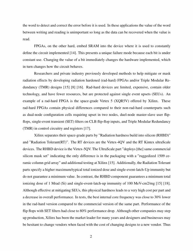
storage elements. When a radiation particle collides with a circuit it leaves a trail of charge as
illustrated by [1] in Figure 2.1. Although this spike in charge is often fleeting the timing can cause
undesired circuit behavior, such as a premature rising edge on a clock line or incorrect value output
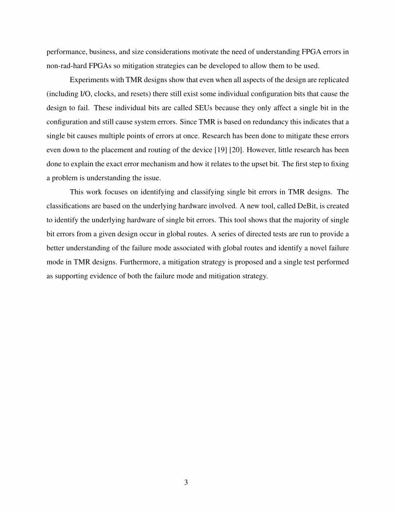
on a register. If the charge is deposited at the right place in an SRAM cell this can cause the value
to change as shown in Figure 2.2. Here the disruption of the transistor opens the gate causing the
gate voltage that was previously held high to transition to a low state. Over the years as feature
sizes continue to shrink, voltages lower, and architectures change the susceptibility of most circuits
to radiation have become more prevalent.
SRAM is of particular importance because it stores bit values. In most applications, SRAM
is used primarily as a storage medium where values are stored as complete words which sit unused
4
Figure 2.1: Radiation effects in semi-conductor devices as shown in [1].
until read out. The advantage in these applications is the memory writing and reading logic can be
modified to contain extra bits with each word to act as Error Correction Codes (ECC) that detect
and correct one or more bit errors. Memory applications can overcome the instability of SRAM
in high radiation environments by storing ECC bits at the same time. This does not prevent errors
from occurring but allows for errors to be caught and corrected before being used.
2.2 FPGA Radiation Errors
The SRAM used in FPGAs have a different use than typical applications. The SRAM in
an FPGA is used to configure basic hardware elements to mimic user-defined hardware circuits.
The hardware element may be as simple as selecting a mux to route a signal or as complex as a
PLL synthesizing an internal clock. These elements are controlled by a set of configuration bits
directly from SRAM. Unlike SRAM used in memory, any change in the SRAM used for FPGA
configuration induces an immediate change in the underlying hardware it controls. The number of
SRAM bits in use depends on the user-defined circuit. If the user-defined circuit is small, fewer
FPGA resources are needed to mimic the circuit. This means there are only a subset of SRAM bits
in use to create the user-defined circuit and the remaining SRAM configuration bits are unused.
Many experiments since have shown that SRAM bits in FPGAs are susceptible to radiation
effects [13] [22] [9] [7] [10]. If the configuration bit modified by radiation affects the user-defined
circuit to the point that the circuit no longer produces the expected result, an error occurs. Radiation
effects causing errors in FPGAs can be classified as hard, persistent, or soft errors. Hard errors
cause permanent damage to the device and do not recover after power cycling or reconfiguration.
5
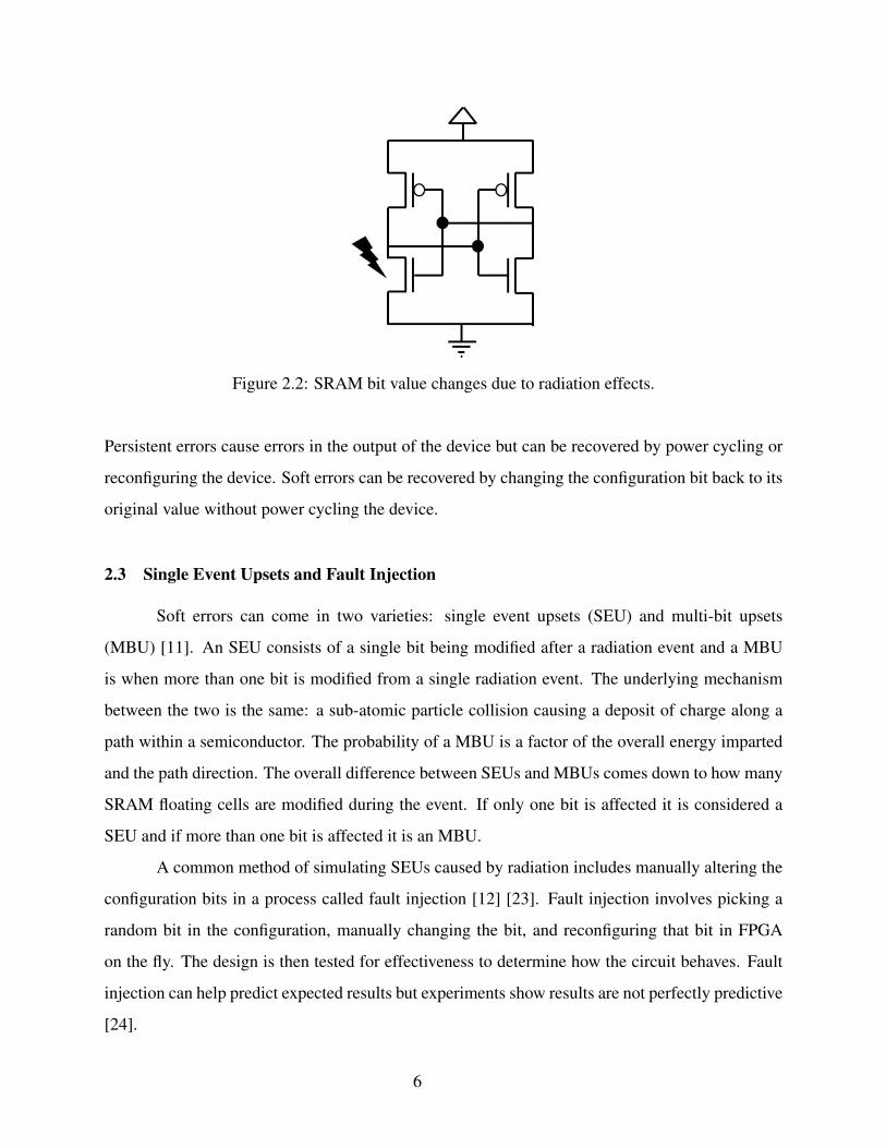
Figure 2.2: SRAM bit value changes due to radiation effects.
Persistent errors cause errors in the output of the device but can be recovered by power cycling or
reconfiguring the device. Soft errors can be recovered by changing the configuration bit back to its
original value without power cycling the device.
2.3 Single Event Upsets and Fault Injection
Soft errors can come in two varieties: single event upsets (SEU) and multi-bit upsets
(MBU) [11]. An SEU consists of a single bit being modified after a radiation event and a MBU
is when more than one bit is modified from a single radiation event. The underlying mechanism
between the two is the same: a sub-atomic particle collision causing a deposit of charge along a
path within a semiconductor. The probability of a MBU is a factor of the overall energy imparted
and the path direction. The overall difference between SEUs and MBUs comes down to how many
SRAM floating cells are modified during the event. If only one bit is affected it is considered a
SEU and if more than one bit is affected it is an MBU.
A common method of simulating SEUs caused by radiation includes manually altering the
configuration bits in a process called fault injection [12] [23]. Fault injection involves picking a
random bit in the configuration, manually changing the bit, and reconfiguring that bit in FPGA
on the fly. The design is then tested for effectiveness to determine how the circuit behaves. Fault
injection can help predict expected results but experiments show results are not perfectly predictive
[24].
6
2.4 Configuration Scrubbing
In an application note released by Xilinx in 2000 partial reconfiguration is used to correct
bit errors in the configuration in a technique called bitstream scrubbing [25]. Bitstream scrubbing
involves reading back the configuration data within the FPGA, evaluating it for errors, and re-
configuring that section while the devices is running. Methods for configuration scrubbing to
improve effectiveness, architecture, and space have been explored by Harding, Stoddard, Heiner,
and others [26] [27] [28] [29]. These architectures include both on-chip and off-chip methods.
Configuration scrubbing techniques repair configuration bit errors after they occur, so they
cannot prevent an error from occurring if the bit affects an actively used circuit. Fuller, et. al.
show configuration scrubbing results in no significant improvement in sensitivity when scrubbing
is performed alone. When scrubbing is combined with other mitigation techniques it provides a
significant improvement in sensitivity [16] [30].
2.5 Triple Modular Redundancy
In a study a year after radiation effects were discovered, R. E. Lyons and W. Venderkulk
present models for failing redundant circuits and introduce the idea of Triple Modular Redundancy
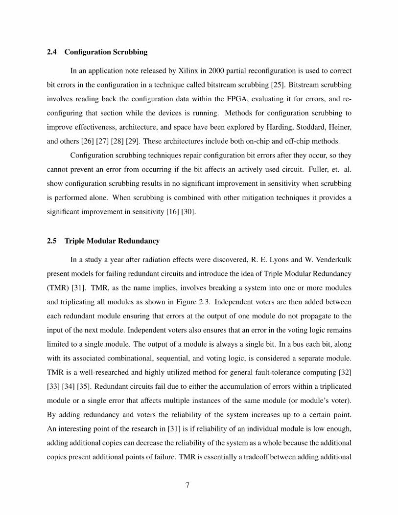
(TMR) [31]. TMR, as the name implies, involves breaking a system into one or more modules
and triplicating all modules as shown in Figure 2.3. Independent voters are then added between
each redundant module ensuring that errors at the output of one module do not propagate to the
input of the next module. Independent voters also ensures that an error in the voting logic remains
limited to a single module. The output of a module is always a single bit. In a bus each bit, along
with its associated combinational, sequential, and voting logic, is considered a separate module.
TMR is a well-researched and highly utilized method for general fault-tolerance computing [32]
[33] [34] [35]. Redundant circuits fail due to either the accumulation of errors within a triplicated
module or a single error that affects multiple instances of the same module (or module’s voter).
By adding redundancy and voters the reliability of the system increases up to a certain point.
An interesting point of the research in [31] is if reliability of an individual module is low enough,
adding additional copies can decrease the reliability of the system as a whole because the additional
copies present additional points of failure. TMR is essentially a tradeoff between adding additional
7
Figure 2.3: Triple modular redundancy.
points of failure and adding redundancy to mask those failures.
2.6 Triple Modular Redundancy in FPGAs
The first known work of using TMR in Virtex FPGAs is from Fuller, et. al. [16] where
they describe the results of using TMR, bitstream scrubbing, and power-tie downs in live neutron
radiation experiments at Los Almos National Laboratory. The end result of adding TMR, bitstream
scrubbing, and mitigating the weak-keepers leads to an impressive 1000x improvement in design
sensitivity. Neither TMR nor bitstream scrubbing alone produce the same results. Although the im-
provement is impressive it does not remove all sources of SEUs or describe the failure mechanism
of the remaining SEUs.
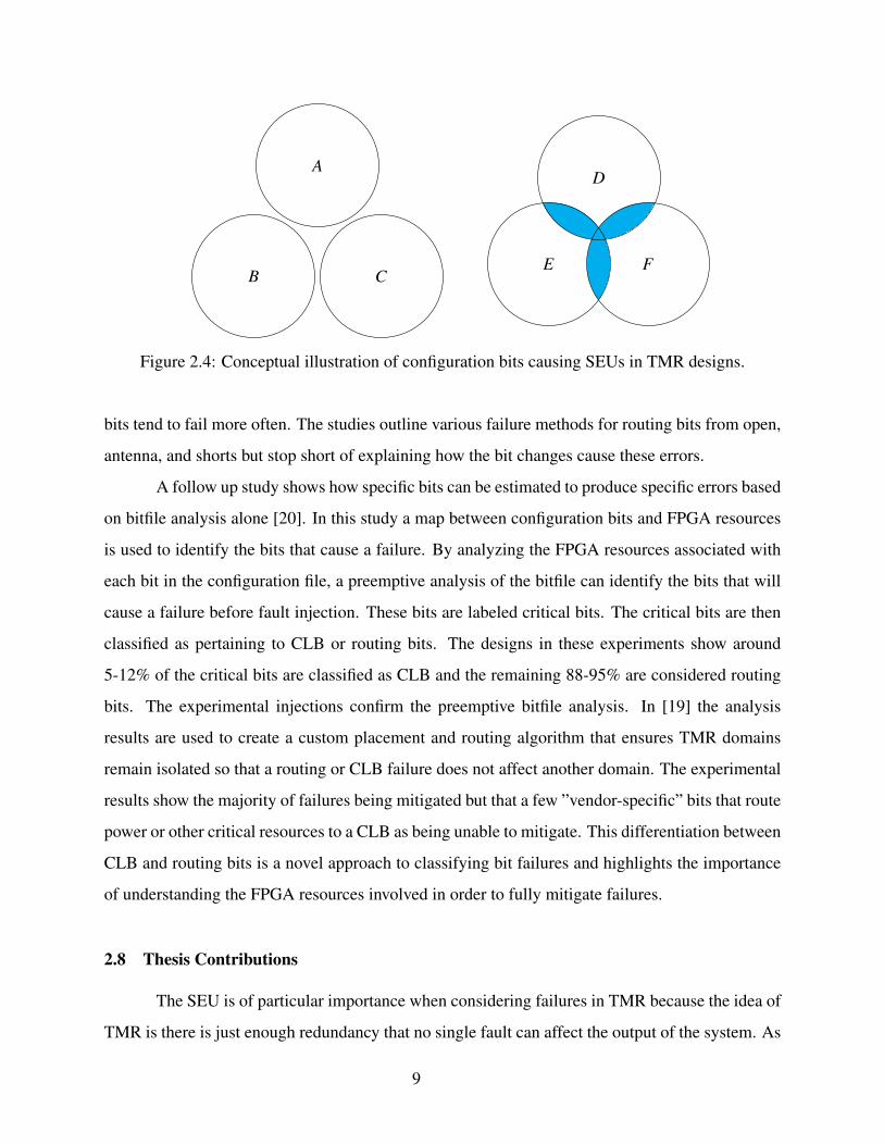
If the original TMR model proposed by [31] were shown as a Venn diagram representing
SEU failures, it would be represented visually in the left in Figure 2.4 where only one domain
would be affected at a time. However, experimental results indicate the error model is actually
better represented in the figure on the right in Figure 2.4 where there are a small number of bits
that can affect multiple domains. The larger the area associated with overlapping domains, the less
the TMR model applies to those created by [31].
2.7 FPGA Root Cause Failure and Classification
A series of studies by Luca Sterpone and colleagues dive deeper in explaining how SEUs
cause multiple domain failures and deserve particular attention due to the similarities between that
work and the work presented in this thesis. In the initial study TMR is shown to be inadequate
for preventing faults after single-bit error injections [36] [37]. In [36] a series of basic functions
(addr8, addr16, mult8) are triplicated with voting logic and implemented with full fault injection
of the used configuration bits. The results show that slices with a higher concentration of allocated
8
A
B C
D
E F
Figure 2.4: Conceptual illustration of configuration bits causing SEUs in TMR designs.
bits tend to fail more often. The studies outline various failure methods for routing bits from open,
antenna, and shorts but stop short of explaining how the bit changes cause these errors.
A follow up study shows how specific bits can be estimated to produce specific errors based
on bitfile analysis alone [20]. In this study a map between configuration bits and FPGA resources
is used to identify the bits that cause a failure. By analyzing the FPGA resources associated with
each bit in the configuration file, a preemptive analysis of the bitfile can identify the bits that will
cause a failure before fault injection. These bits are labeled critical bits. The critical bits are then
classified as pertaining to CLB or routing bits. The designs in these experiments show around
5-12% of the critical bits are classified as CLB and the remaining 88-95% are considered routing
bits. The experimental injections confirm the preemptive bitfile analysis. In [19] the analysis
results are used to create a custom placement and routing algorithm that ensures TMR domains
remain isolated so that a routing or CLB failure does not affect another domain. The experimental
results show the majority of failures being mitigated but that a few ”vendor-specific” bits that route
power or other critical resources to a CLB as being unable to mitigate. This differentiation between
CLB and routing bits is a novel approach to classifying bit failures and highlights the importance
of understanding the FPGA resources involved in order to fully mitigate failures.
2.8 Thesis Contributions
The SEU is of particular importance when considering failures in TMR because the idea of
TMR is there is just enough redundancy that no single fault can affect the output of the system. As
9
SEUs in TMR are understood and mitigated, TMR can have a larger impact on overall reliability
by providing the true redundancy it is intended to provide. As will be shown in this thesis, an
understanding of the architecture of the FPGA is needed to understand how an SEU can cause
multiple domains to fail. For this thesis, the Xilinx Virtex series 7 architecture was used due to its
prevalence and availability with the hope that the techniques employed could be used on any future
architecture.
Analysis performed to find exactly why a failure occurs is called root-cause failure analysis.
This work performs a root-cause failure analysis of configuration bit failures in SRAM-based FP-
GAs. This is done by creating a tool called DeBit to identifying the hardware resources associated
with single bit configuration errors in TMR. DeBit is used to classify SEUs based on the underly-
ing hardware and show that the majority of SEUs are associated with global routing networks. A
series of directed tests are run to more fully understand the root-cause of failure with global routes.
This understanding is used to propose a novel failure mode of SEUs in TMR in Virtex 7 architec-
tures. The novel failure mode is identified in a TMR design and an associated mitigation method
within the same PIP junction structure is also proposed. A single mitigation test is performed as
further evidence of the novel failure mode and mitigation strategy. It is hoped this more thorough
understanding of SEUs will aid in developing more independence between domains to create more
reliable FPGA designs implementing TMR.
10
CHAPTER 3. XILINX SERIES 7 ARCHITECTURE
This chapter focuses on the architecture of the Xilinx Series 7 FPGA and the various circuit
elements that are controlled by the configuration bits. The Series 7 architecture was chosen because
of it ubiquity and wide resource range as well as because the Virtex 5 space-grade part is slated for
obsolescence. To understand how the configuration bits modify the FPGA behavior, it is useful to
understand the architecture of the FPGA. This helps lay the groundwork for how failures occur and
the work involved in understanding the effects of SEUs in these FPGAs. The chapter organizes
the architecture of the FPGA starting at the highest level and drilling into the sub-systems until the
lowest configurable elements are discussed.
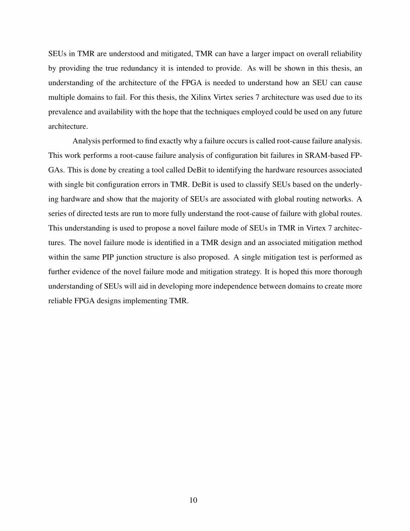
3.1 Clocking Region
The hardware resources in Xilinx Virtex-7 FPGAs are organized into several categories,
the largest of which is the clocking region. A clocking region is a region of logic within the
FPGA where all flip flops have access to the same set of clock lines. Clock regions are defined
horizontally as the width from the edge of the device to the clock backbone and vertically defined
as a span of 50 Configurable Logic Blocks (CLB) tiles [38]. The clocking regions allow access to
12 global clock nets each of which can be chosen from among 32 different clocks. Clock regions
are defined by their spatial location relative to a clock backbone near the center or edge of the
chip. The clock backbone runs vertically and clock regions are either left or right of the backbone.
Series 7 FPGAs can have anywhere between 1 and 24 clocking regions [38]. Figure 3.1 shows the
10 clocking regions for the part xc7a200tsbg484-1. The color bands on the left and right sides of
this figure represent the various input and output pins available on the FPGA device.
11
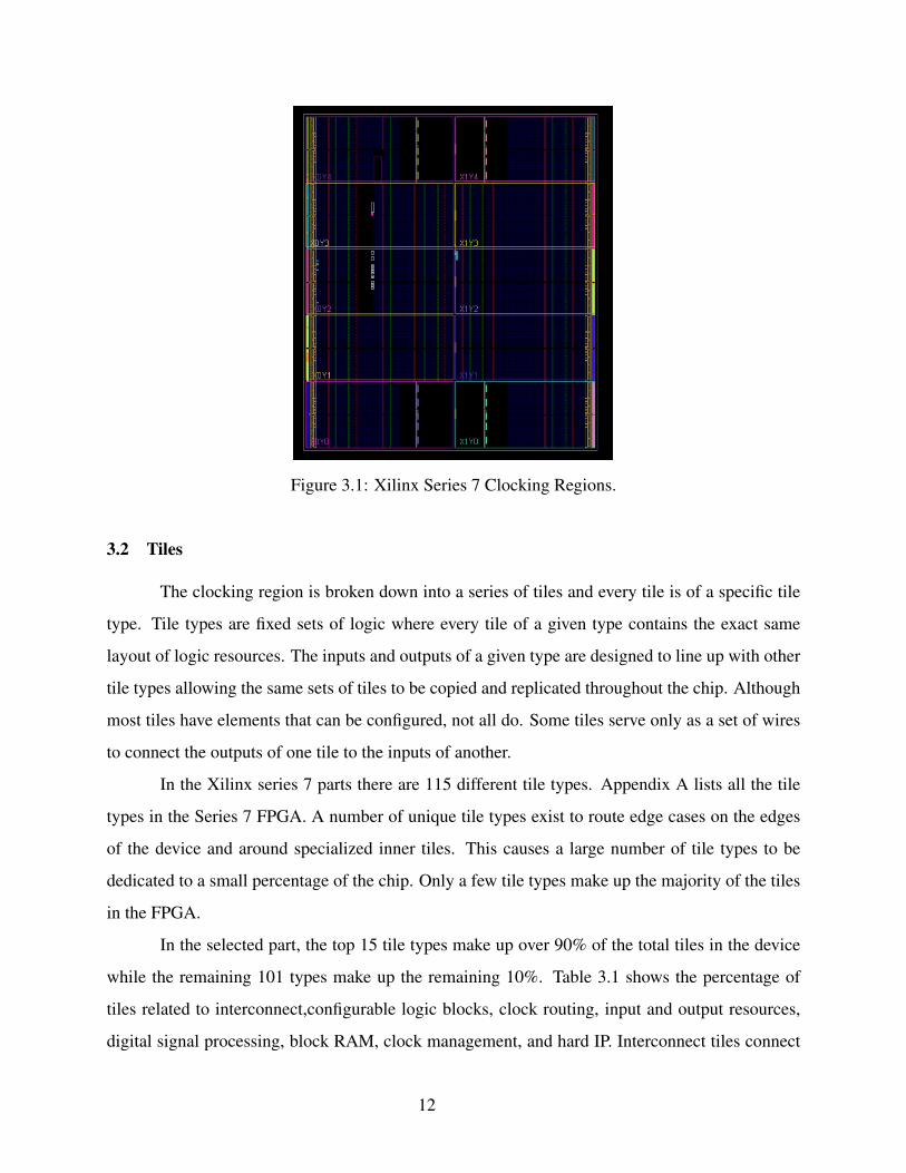
Figure 3.1: Xilinx Series 7 Clocking Regions.
3.2 Tiles
The clocking region is broken down into a series of tiles and every tile is of a specific tile
type. Tile types are fixed sets of logic where every tile of a given type contains the exact same
layout of logic resources. The inputs and outputs of a given type are designed to line up with other
tile types allowing the same sets of tiles to be copied and replicated throughout the chip. Although
most tiles have elements that can be configured, not all do. Some tiles serve only as a set of wires
to connect the outputs of one tile to the inputs of another.
In the Xilinx series 7 parts there are 115 different tile types. Appendix A lists all the tile
types in the Series 7 FPGA. A number of unique tile types exist to route edge cases on the edges
of the device and around specialized inner tiles. This causes a large number of tile types to be
dedicated to a small percentage of the chip. Only a few tile types make up the majority of the tiles
in the FPGA.
In the selected part, the top 15 tile types make up over 90% of the total tiles in the device
while the remaining 101 types make up the remaining 10%. Table 3.1 shows the percentage of
tiles related to interconnect,configurable logic blocks, clock routing, input and output resources,
digital signal processing, block RAM, clock management, and hard IP. Interconnect tiles connect
12
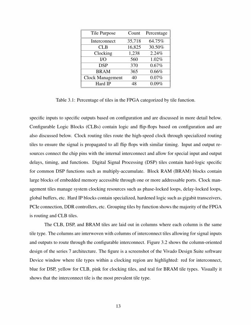
Tile Purpose Count Percentage
Interconnect 35,718 64.75%
CLB 16,825 30.50%
Clocking 1,238 2.24%
I/O 560 1.02%
DSP 370 0.67%
BRAM 365 0.66%
Clock Management 40 0.07%
Hard IP 48 0.09%
Table 3.1: Percentage of tiles in the FPGA categorized by tile function.
specific inputs to specific outputs based on configuration and are discussed in more detail below.
Configurable Logic Blocks (CLBs) contain logic and flip-flops based on configuration and are
also discussed below. Clock routing tiles route the high-speed clock through specialized routing
tiles to ensure the signal is propagated to all flip flops with similar timing. Input and output re-
sources connect the chip pins with the internal interconnect and allow for special input and output
delays, timing, and functions. Digital Signal Processing (DSP) tiles contain hard-logic specific
for common DSP functions such as multiply-accumulate. Block RAM (BRAM) blocks contain
large blocks of embedded memory accessible through one or more addressable ports. Clock man-
agement tiles manage system clocking resources such as phase-locked loops, delay-locked loops,
global buffers, etc. Hard IP blocks contain specialized, hardened logic such as gigabit transceivers,
PCIe connection, DDR controllers, etc. Grouping tiles by function shows the majority of the FPGA
is routing and CLB tiles.
The CLB, DSP, and BRAM tiles are laid out in columns where each column is the same
tile type. The columns are interwoven with columns of interconnect tiles allowing for signal inputs
and outputs to route through the configurable interconnect. Figure 3.2 shows the column-oriented
design of the series 7 architecture. The figure is a screenshot of the Vivado Design Suite software
Device window where tile types within a clocking region are highlighted: red for interconnect,
blue for DSP, yellow for CLB, pink for clocking tiles, and teal for BRAM tile types. Visually it
shows that the interconnect tile is the most prevalent tile type.
13
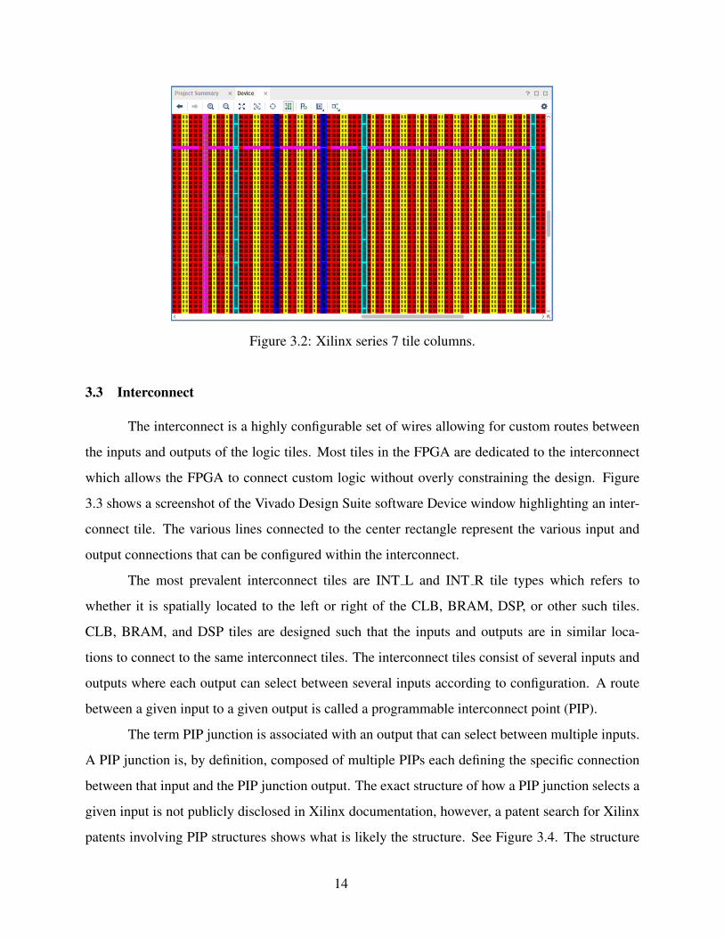
Figure 3.2: Xilinx series 7 tile columns.
3.3 Interconnect
The interconnect is a highly configurable set of wires allowing for custom routes between
the inputs and outputs of the logic tiles. Most tiles in the FPGA are dedicated to the interconnect
which allows the FPGA to connect custom logic without overly constraining the design. Figure
3.3 shows a screenshot of the Vivado Design Suite software Device window highlighting an inter-
connect tile. The various lines connected to the center rectangle represent the various input and
output connections that can be configured within the interconnect.
The most prevalent interconnect tiles are INT L and INT R tile types which refers to
whether it is spatially located to the left or right of the CLB, BRAM, DSP, or other such tiles.
CLB, BRAM, and DSP tiles are designed such that the inputs and outputs are in similar loca-
tions to connect to the same interconnect tiles. The interconnect tiles consist of several inputs and
outputs where each output can select between several inputs according to configuration. A route
between a given input to a given output is called a programmable interconnect point (PIP).
The term PIP junction is associated with an output that can select between multiple inputs.
A PIP junction is, by definition, composed of multiple PIPs each defining the specific connection
between that input and the PIP junction output. The exact structure of how a PIP junction selects a
given input is not publicly disclosed in Xilinx documentation, however, a patent search for Xilinx
patents involving PIP structures shows what is likely the structure. See Figure 3.4. The structure
14
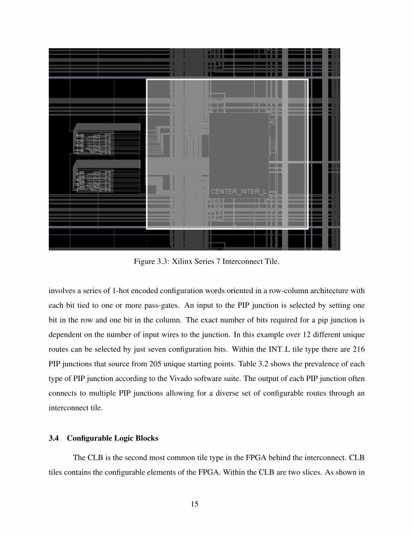
Figure 3.3: Xilinx Series 7 Interconnect Tile.
involves a series of 1-hot encoded configuration words oriented in a row-column architecture with
each bit tied to one or more pass-gates. An input to the PIP junction is selected by setting one
bit in the row and one bit in the column. The exact number of bits required for a pip junction is
dependent on the number of input wires to the junction. In this example over 12 different unique
routes can be selected by just seven configuration bits. Within the INT L tile type there are 216
PIP junctions that source from 205 unique starting points. Table 3.2 shows the prevalence of each
type of PIP junction according to the Vivado software suite. The output of each PIP junction often
connects to multiple PIP junctions allowing for a diverse set of configurable routes through an
interconnect tile.
3.4 Configurable Logic Blocks
The CLB is the second most common tile type in the FPGA behind the interconnect. CLB
tiles contains the configurable elements of the FPGA. Within the CLB are two slices. As shown in
15
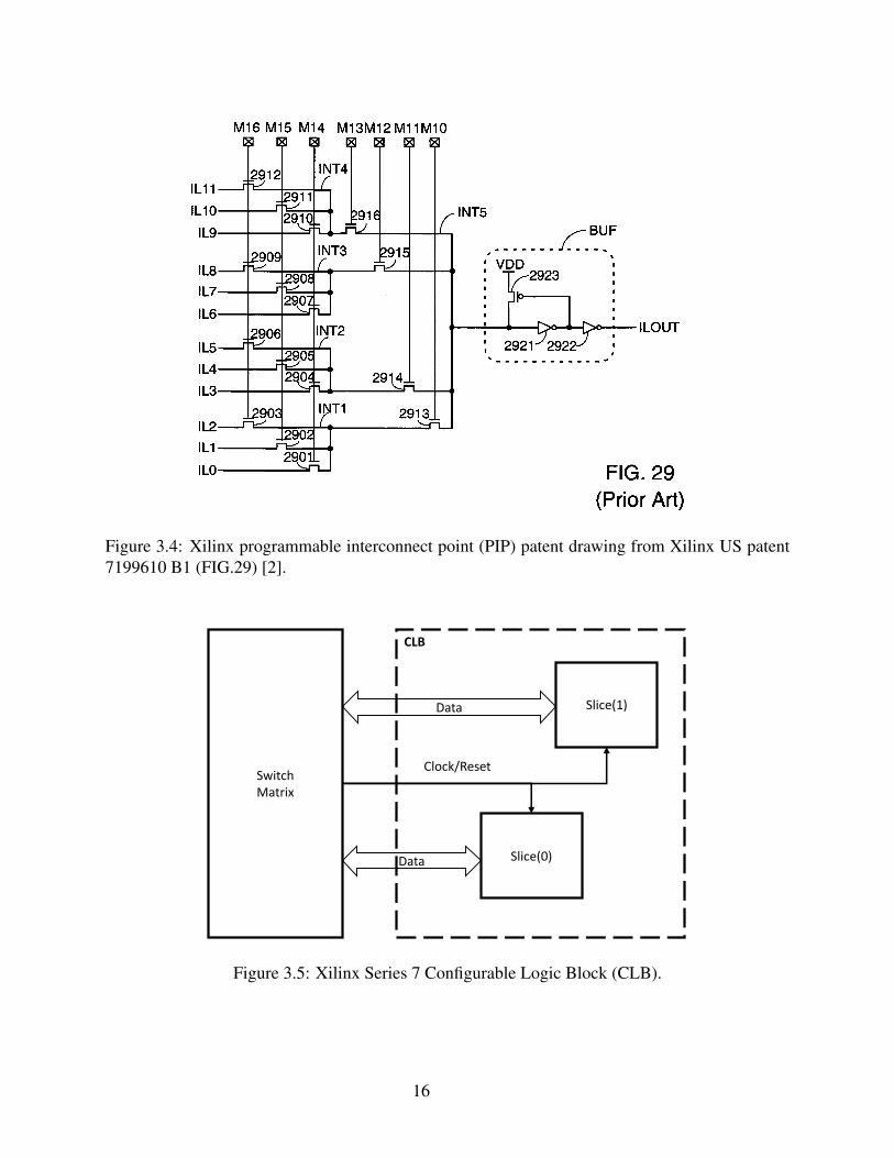
Figure 3.4: Xilinx programmable interconnect point (PIP) patent drawing from Xilinx US patent
7199610 B1 (FIG.29) [2].
Switch
Matrix
Data
Slice(1)Data
Slice(0)
Clock/Reset
CLB
Figure 3.5: Xilinx Series 7 Configurable Logic Block (CLB).
16
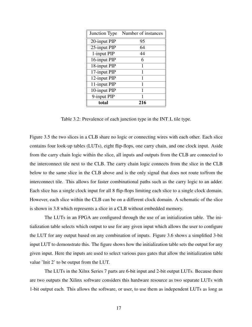
Junction Type Number of instances
20-input PIP 95
25-input PIP 64
1-input PIP 44
16-input PIP 6
18-input PIP 1
17-input PIP 1
12-input PIP 1
11-input PIP 1
10-input PIP 1
9-input PIP 1
total 216
Table 3.2: Prevalence of each junction type in the INT L tile type.
Figure 3.5 the two slices in a CLB share no logic or connecting wires with each other. Each slice
contains four look-up tables (LUTs), eight flip-flops, one carry chain, and one clock input. Aside
from the carry chain logic within the slice, all inputs and outputs from the CLB are connected to
the interconnect tile next to the CLB. The carry chain logic connects from the slice in the CLB
below to the same slice in the CLB above and is the only signal that does not route to/from the
interconnect tile. This allows for faster combinational paths such as the carry logic to an adder.
Each slice has a single clock input for all 8 flip-flops limiting each slice to a single clock domain.
However, each slice within the CLB can be on a different clock domain. A schematic of the slice
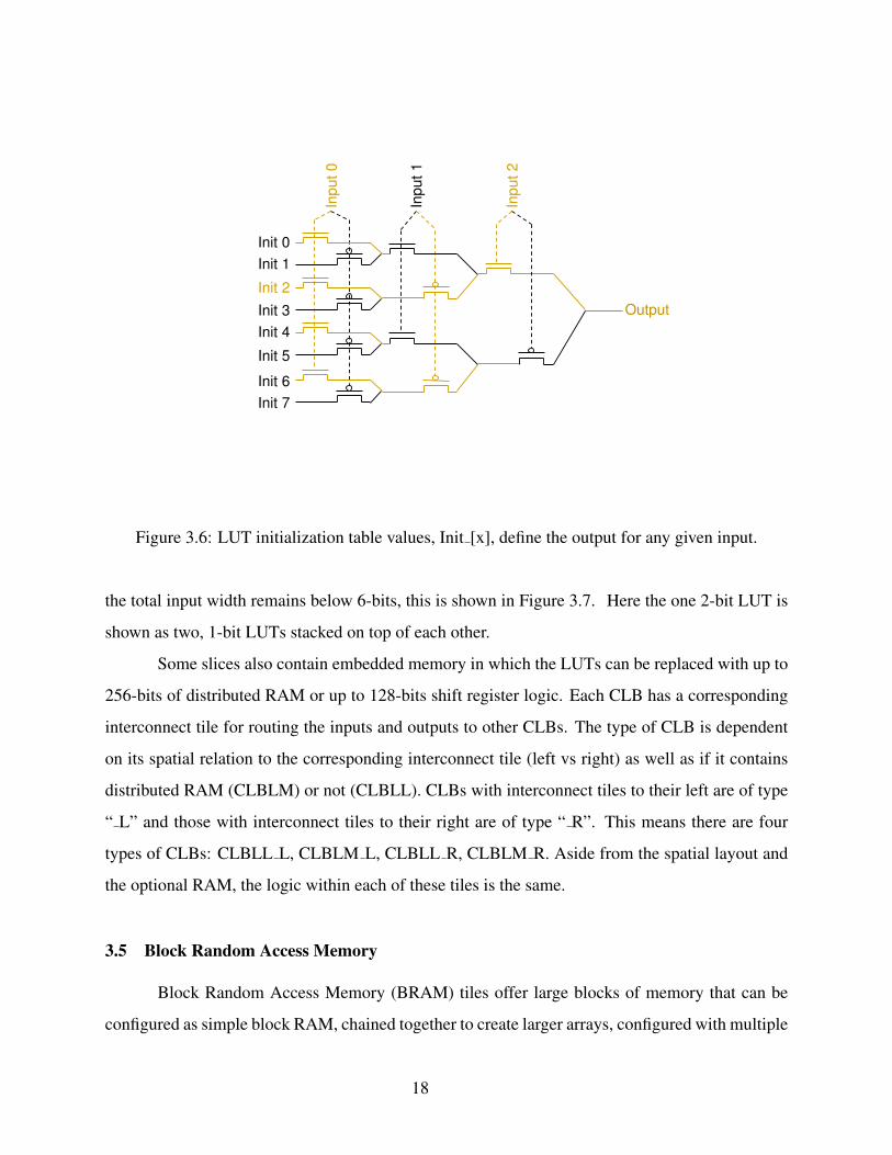
is shown in 3.8 which represents a slice in a CLB without embedded memory.
The LUTs in an FPGA are configured through the use of an initialization table. The ini-
tialization table selects which output to use for any given input which allows the user to configure
the LUT for any output based on any combination of inputs. Figure 3.6 shows a simplified 3-bit
input LUT to demonstrate this. The figure shows how the initialization table sets the output for any
given input. Here the inputs are used to select various pass gates that allow the initialization table
value ’Init 2’ to be output from the LUT.
The LUTs in the Xilnx Series 7 parts are 6-bit input and 2-bit output LUTs. Because there
are two outputs the Xilinx software considers this hardware resource as two separate LUTs with
1-bit output each. This allows the software, or user, to use them as independent LUTs as long as
17
Init 0
Init 1
Output
Input
1
Init 2
Init 3
Init 4
Init 5
Init 6
Init 7
Input
0
Input
2
Figure 3.6: LUT initialization table values, Init [x], define the output for any given input.
the total input width remains below 6-bits, this is shown in Figure 3.7. Here the one 2-bit LUT is
shown as two, 1-bit LUTs stacked on top of each other.
Some slices also contain embedded memory in which the LUTs can be replaced with up to
256-bits of distributed RAM or up to 128-bits shift register logic. Each CLB has a corresponding
interconnect tile for routing the inputs and outputs to other CLBs. The type of CLB is dependent
on its spatial relation to the corresponding interconnect tile (left vs right) as well as if it contains
distributed RAM (CLBLM) or not (CLBLL). CLBs with interconnect tiles to their left are of type
“ L” and those with interconnect tiles to their right are of type “ R”. This means there are four
types of CLBs: CLBLL L, CLBLM L, CLBLL R, CLBLM R. Aside from the spatial layout and
the optional RAM, the logic within each of these tiles is the same.
3.5 Block Random Access Memory
Block Random Access Memory (BRAM) tiles offer large blocks of memory that can be
configured as simple block RAM, chained together to create larger arrays, configured with multiple
18
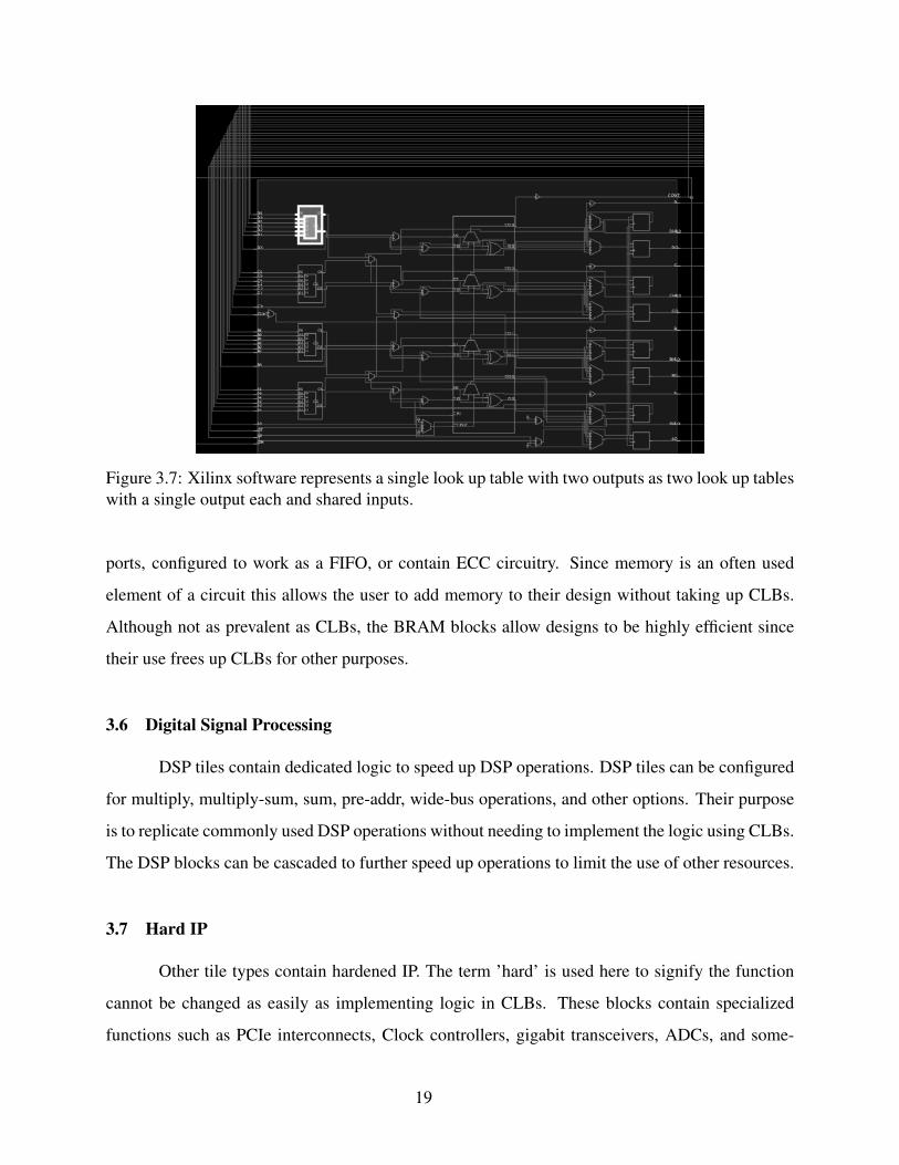
Figure 3.7: Xilinx software represents a single look up table with two outputs as two look up tables
with a single output each and shared inputs.
ports, configured to work as a FIFO, or contain ECC circuitry. Since memory is an often used
element of a circuit this allows the user to add memory to their design without taking up CLBs.
Although not as prevalent as CLBs, the BRAM blocks allow designs to be highly efficient since
their use frees up CLBs for other purposes.
3.6 Digital Signal Processing
DSP tiles contain dedicated logic to speed up DSP operations. DSP tiles can be configured
for multiply, multiply-sum, sum, pre-addr, wide-bus operations, and other options. Their purpose
is to replicate commonly used DSP operations without needing to implement the logic using CLBs.
The DSP blocks can be cascaded to further speed up operations to limit the use of other resources.
3.7 Hard IP
Other tile types contain hardened IP. The term ’hard’ is used here to signify the function
cannot be changed as easily as implementing logic in CLBs. These blocks contain specialized
functions such as PCIe interconnects, Clock controllers, gigabit transceivers, ADCs, and some-
19
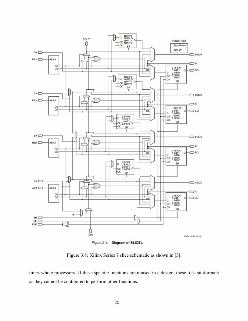
Figure 3.8: Xilinx Series 7 slice schematic as shown in [3].
times whole processors. If these specific functions are unused in a design, these tiles sit dormant
as they cannot be configured to perform other functions.
20
3.8 Bitstream Configuration
The final part of the architecture relates to how the configuration bits are organized within
the FPGA. This information is found in the Xilinx Configuration Guide [14]. The bitfile contains
header information and configuration data.
The header information is for word-alignment, version, details about the layout of the data,
and other housekeeping tasks along with the configuration data. The header does not get stored in
the FPGA as configuration directly but is used to know how to parse the subsequent data within
the bitfile and set up the FPGA registers to prepare for configuration.
The configuration data in the bitfile is separated into a series of packets where each packet
has a header that defines the operation of the subsequent data. There are two packet types: type
1 and type 2. Type 1 packets are used for general register access. This can be used for encrypted
bitstream configuration, watchdog timer use, general debugging and access, and setting the address
for the configuration frames. Type 1 packets always have an associated address for specifying
which register to set and the value of the register. Type 2 packets are used for bulk data, such as the
configuration frames. As such, they only contain a short header to define if the bulk data is read,
written, or omitted and the number of words in the packet.
The packet types in the bitfile that are used to configure the FPGA are type 2 packet frames.
Type 2 packets contain the configuration frames. configuration frames are 101 words long (32-bit
words) and are addressable using the Frame Address Register (FAR) of the FPGA. The FAR is a
26-bit word broken into a type, top/bottom, row, column, and minor address as shown in table 3.3.
When the FAR is set the configuration data loaded into the FPGA is loaded into that configuration
frame. After loading in the configuration data frame the FAR is automatically incremented to the
next address.
A configuration frame contains the configuration data for the tiles corresponding to the
addressed row/column. The row/column indicated in the FAR is not the same index values for the
row/column of a given tile. The Xininx documentation does not provide information about the map
between the FAR row/column and the tile row/column. Typically, the configuration data for a given
FAR contains part of the configuration for multiple tiles. The configuration data also contains a
single ECC word for error correction/detection. To prevent having to set the FAR before loading
every frame, the FPGA will automatically increment the FAR after the frame data is loaded. Xilinx
21
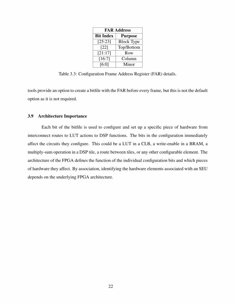
FAR Address
Bit Index Purpose
[25:23] Block Type
[22] Top/Bottom
[21:17] Row
[16:7] Column
[6:0] Minor
Table 3.3: Configuration Frame Address Register (FAR) details.
tools provide an option to create a bitfile with the FAR before every frame, but this is not the default
option as it is not required.
3.9 Architecture Importance
Each bit of the bitfile is used to configure and set up a specific piece of hardware from
interconnect routes to LUT actions to DSP functions. The bits in the configuration immediately
affect the circuits they configure. This could be a LUT in a CLB, a write-enable in a BRAM, a
multiply-sum operation in a DSP tile, a route between tiles, or any other configurable element. The
architecture of the FPGA defines the function of the individual configuration bits and which pieces
of hardware they affect. By association, identifying the hardware elements associated with an SEU
depends on the underlying FPGA architecture.
22
CHAPTER 4. DEBIT: A BIT ANALYSIS TOOL
In order to classify SEUs by the underlying hardware involved, the hardware associated
with a given bit in the bitfile must be known. However, vendor tools do not provide a mechanism
for identifying the hardware resources associated with a bit in the bitfile. Vendor tools go the
opposite direction, providing a bitfile for a given set of hardware. Outside of SEU reliability the
author is unaware of another application that needs to know the hardware affected by a given bit in
the bitfile.
To understand which element(s) of hardware are affected by a given bit in the bitfile a new
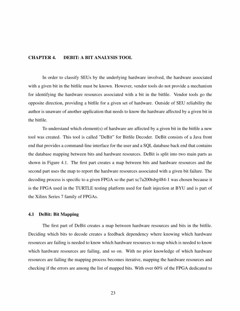
tool was created. This tool is called ”DeBit” for Bitfile Decoder. DeBit consists of a Java front
end that provides a command-line interface for the user and a SQL database back end that contains
the database mapping between bits and hardware resources. DeBit is split into two main parts as
shown in Figure 4.1. The first part creates a map between bits and hardware resources and the
second part uses the map to report the hardware resources associated with a given bit failure. The
decoding process is specific to a given FPGA so the part xc7a200tsbg484-1 was chosen because it
is the FPGA used in the TURTLE testing platform used for fault injection at BYU and is part of
the Xilinx Series 7 family of FPGAs.
4.1 DeBit: Bit Mapping
The first part of DeBit creates a map between hardware resources and bits in the bitfile.
Deciding which bits to decode creates a feedback dependency where knowing which hardware
resources are failing is needed to know which hardware resources to map which is needed to know
which hardware resources are failing, and so on. With no prior knowledge of which hardware
resources are failing the mapping process becomes iterative, mapping the hardware resources and
checking if the errors are among the list of mapped bits. With over 60% of the FPGA dedicated to
23
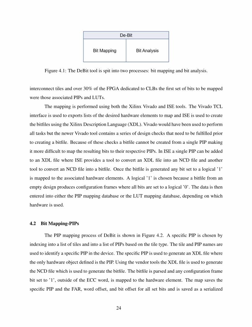
Figure 4.1: The DeBit tool is spit into two processes: bit mapping and bit analysis.
interconnect tiles and over 30% of the FPGA dedicated to CLBs the first set of bits to be mapped
were those associated PIPs and LUTs.
The mapping is performed using both the Xilinx Vivado and ISE tools. The Vivado TCL
interface is used to exports lists of the desired hardware elements to map and ISE is used to create
the bitfiles using the Xilinx Description Language (XDL). Vivado would have been used to perform
all tasks but the newer Vivado tool contains a series of design checks that need to be fulfilled prior
to creating a bitfile. Because of these checks a bitfile cannot be created from a single PIP making
it more difficult to map the resulting bits to their respective PIPs. In ISE a single PIP can be added
to an XDL file where ISE provides a tool to convert an XDL file into an NCD file and another
tool to convert an NCD file into a bitfile. Once the bitfile is generated any bit set to a logical ’1’
is mapped to the associated hardware elements. A logical ’1’ is chosen because a bitfile from an
empty design produces configuration frames where all bits are set to a logical ’0’. The data is then
entered into either the PIP mapping database or the LUT mapping database, depending on which
hardware is used.
4.2 Bit Mapping-PIPs
The PIP mapping process of DeBit is shown in Figure 4.2. A specific PIP is chosen by
indexing into a list of tiles and into a list of PIPs based on the tile type. The tile and PIP names are
used to identify a specific PIP in the device. The specific PIP is used to generate an XDL file where
the only hardware object defined is the PIP. Using the vendor tools the XDL file is used to generate
the NCD file which is used to generate the bitfile. The bitfile is parsed and any configuration frame
bit set to ’1’, outside of the ECC word, is mapped to the hardware element. The map saves the
specific PIP and the FAR, word offset, and bit offset for all set bits and is saved as a serialized
24
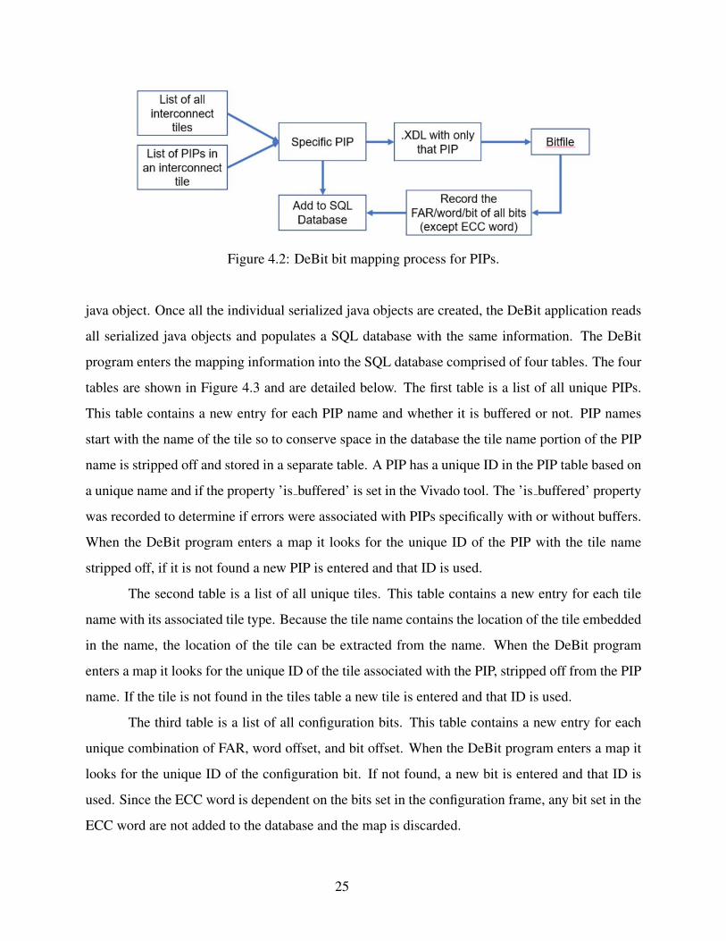
Figure 4.2: DeBit bit mapping process for PIPs.
java object. Once all the individual serialized java objects are created, the DeBit application reads
all serialized java objects and populates a SQL database with the same information. The DeBit
program enters the mapping information into the SQL database comprised of four tables. The four
tables are shown in Figure 4.3 and are detailed below. The first table is a list of all unique PIPs.
This table contains a new entry for each PIP name and whether it is buffered or not. PIP names
start with the name of the tile so to conserve space in the database the tile name portion of the PIP
name is stripped off and stored in a separate table. A PIP has a unique ID in the PIP table based on
a unique name and if the property ’is buffered’ is set in the Vivado tool. The ’is buffered’ property
was recorded to determine if errors were associated with PIPs specifically with or without buffers.
When the DeBit program enters a map it looks for the unique ID of the PIP with the tile name
stripped off, if it is not found a new PIP is entered and that ID is used.
The second table is a list of all unique tiles. This table contains a new entry for each tile
name with its associated tile type. Because the tile name contains the location of the tile embedded
in the name, the location of the tile can be extracted from the name. When the DeBit program
enters a map it looks for the unique ID of the tile associated with the PIP, stripped off from the PIP
name. If the tile is not found in the tiles table a new tile is entered and that ID is used.
The third table is a list of all configuration bits. This table contains a new entry for each
unique combination of FAR, word offset, and bit offset. When the DeBit program enters a map it
looks for the unique ID of the configuration bit. If not found, a new bit is entered and that ID is
used. Since the ECC word is dependent on the bits set in the configuration frame, any bit set in the
ECC word are not added to the database and the map is discarded.
25
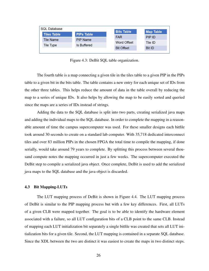
Figure 4.3: DeBit SQL table organization.
The fourth table is a map connecting a given tile in the tiles table to a given PIP in the PIPs
table to a given bit in the bits table. The table contains a new entry for each unique set of IDs from
the other three tables. This helps reduce the amount of data in the table overall by reducing the
map to a series of unique IDs. It also helps by allowing the map to be easily sorted and queried
since the maps are a series of IDs instead of strings.
Adding the data to the SQL database is split into two parts, creating serialized java maps
and adding the individual maps to the SQL database. In order to complete the mapping in a reason-
able amount of time the campus supercomputer was used. For these smaller designs each bitfile
took around 30 seconds to create on a standard lab computer. With 35,718 dedicated interconnect
tiles and over 83 million PIPs in the chosen FPGA the total time to compile the mapping, if done
serially, would take around 79 years to complete. By splitting this process between several thou-
sand compute notes the mapping occurred in just a few weeks. The supercomputer executed the
DeBit step to compile a serialized java object. Once complete, DeBit is used to add the serialized
java maps to the SQL database and the java object is discarded.
4.3 Bit Mapping-LUTs
The LUT mapping process of DeBit is shown in Figure 4.4. The LUT mapping process
of DeBit is similar to the PIP mapping process but with a few key differences. First, all LUTs
of a given CLB were mapped together. The goal is to be able to identify the hardware element
associated with a failure, so all LUT configuration bits of a CLB point to the same CLB. Instead
of mapping each LUT initialization bit separately a single bitfile was created that sets all LUT ini-
tialization bits for a given tile. Second, the LUT mapping is contained in a separate SQL database.
Since the XDL between the two are distinct it was easiest to create the maps in two distinct steps.
26
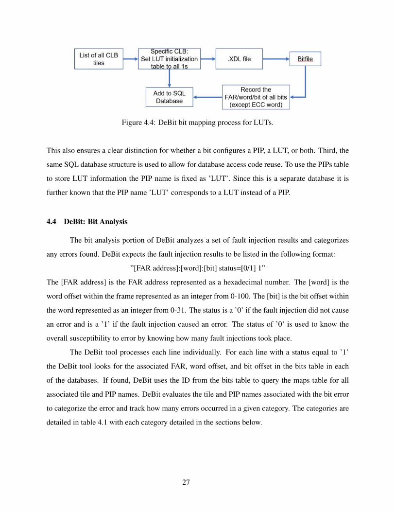
Figure 4.4: DeBit bit mapping process for LUTs.
This also ensures a clear distinction for whether a bit configures a PIP, a LUT, or both. Third, the
same SQL database structure is used to allow for database access code reuse. To use the PIPs table
to store LUT information the PIP name is fixed as ’LUT’. Since this is a separate database it is
further known that the PIP name ’LUT’ corresponds to a LUT instead of a PIP.
4.4 DeBit: Bit Analysis
The bit analysis portion of DeBit analyzes a set of fault injection results and categorizes
any errors found. DeBit expects the fault injection results to be listed in the following format:
”[FAR address]:[word]:[bit] status=[0/1] 1”
The [FAR address] is the FAR address represented as a hexadecimal number. The [word] is the
word offset within the frame represented as an integer from 0-100. The [bit] is the bit offset within
the word represented as an integer from 0-31. The status is a ’0’ if the fault injection did not cause
an error and is a ’1’ if the fault injection caused an error. The status of ’0’ is used to know the
overall susceptibility to error by knowing how many fault injections took place.
The DeBit tool processes each line individually. For each line with a status equal to ’1’
the DeBit tool looks for the associated FAR, word offset, and bit offset in the bits table in each
of the databases. If found, DeBit uses the ID from the bits table to query the maps table for all
associated tile and PIP names. DeBit evaluates the tile and PIP names associated with the bit error
to categorize the error and track how many errors occurred in a given category. The categories are
detailed in table 4.1 with each category detailed in the sections below.
27
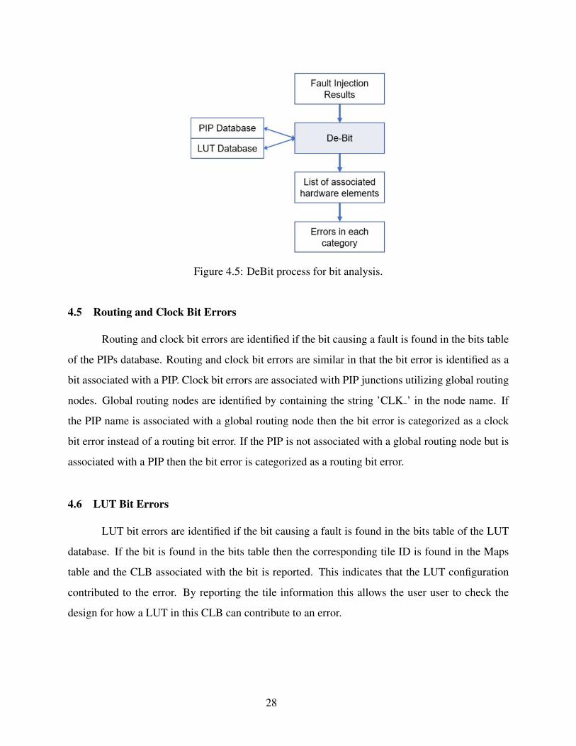
Figure 4.5: DeBit process for bit analysis.
4.5 Routing and Clock Bit Errors
Routing and clock bit errors are identified if the bit causing a fault is found in the bits table
of the PIPs database. Routing and clock bit errors are similar in that the bit error is identified as a
bit associated with a PIP. Clock bit errors are associated with PIP junctions utilizing global routing
nodes. Global routing nodes are identified by containing the string ’CLK ’ in the node name. If
the PIP name is associated with a global routing node then the bit error is categorized as a clock
bit error instead of a routing bit error. If the PIP is not associated with a global routing node but is
associated with a PIP then the bit error is categorized as a routing bit error.
4.6 LUT Bit Errors
LUT bit errors are identified if the bit causing a fault is found in the bits table of the LUT
database. If the bit is found in the bits table then the corresponding tile ID is found in the Maps
table and the CLB associated with the bit is reported. This indicates that the LUT configuration
contributed to the error. By reporting the tile information this allows the user user to check the
design for how a LUT in this CLB can contribute to an error.
28
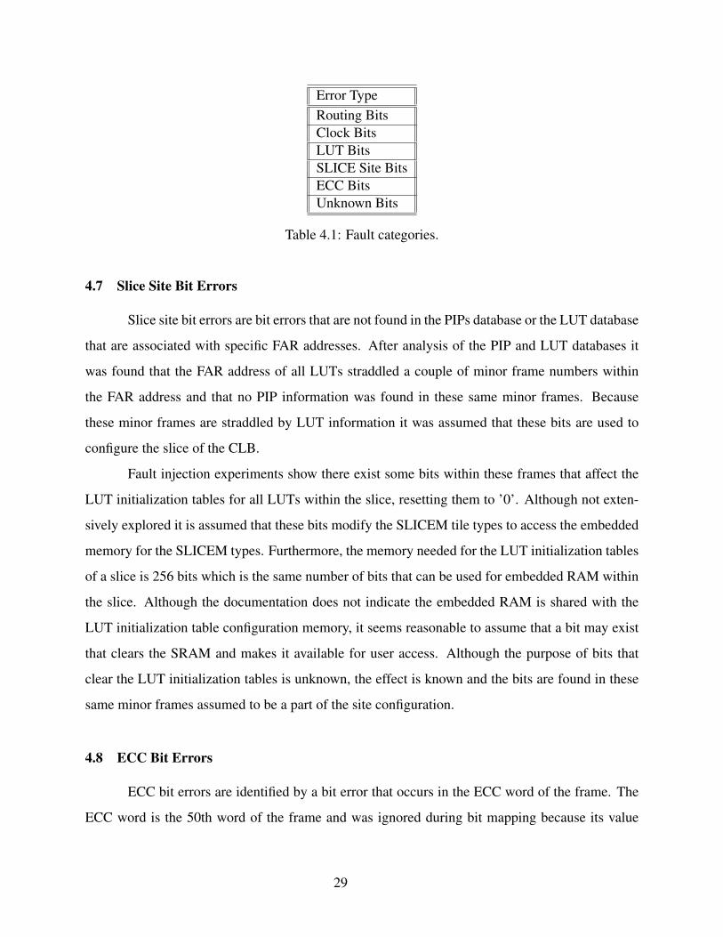
Error Type
Routing Bits
Clock Bits
LUT Bits
SLICE Site Bits
ECC Bits
Unknown Bits
Table 4.1: Fault categories.
4.7 Slice Site Bit Errors
Slice site bit errors are bit errors that are not found in the PIPs database or the LUT database
that are associated with specific FAR addresses. After analysis of the PIP and LUT databases it
was found that the FAR address of all LUTs straddled a couple of minor frame numbers within
the FAR address and that no PIP information was found in these same minor frames. Because
these minor frames are straddled by LUT information it was assumed that these bits are used to
configure the slice of the CLB.
Fault injection experiments show there exist some bits within these frames that affect the
LUT initialization tables for all LUTs within the slice, resetting them to ’0’. Although not exten-
sively explored it is assumed that these bits modify the SLICEM tile types to access the embedded
memory for the SLICEM types. Furthermore, the memory needed for the LUT initialization tables
of a slice is 256 bits which is the same number of bits that can be used for embedded RAM within
the slice. Although the documentation does not indicate the embedded RAM is shared with the
LUT initialization table configuration memory, it seems reasonable to assume that a bit may exist
that clears the SRAM and makes it available for user access. Although the purpose of bits that
clear the LUT initialization tables is unknown, the effect is known and the bits are found in these
same minor frames assumed to be a part of the site configuration.
4.8 ECC Bit Errors
ECC bit errors are identified by a bit error that occurs in the ECC word of the frame. The
ECC word is the 50th word of the frame and was ignored during bit mapping because its value
29
depends on the configuration of the frame. If an error from the fault injection results lists the word
associated with the ECC word then the bit is identified as an ECC bit error.
4.9 Unknown Bit Errors
Unknown bit errors are identified as bits that occur that are not in the ECC word and not
identified in the bits table in either the PIP or LUT databases. These bits are used to identify if
the iterative process of mapping the device configuration bits needs to be more extensive. Since
the databases currently only contain routing and LUT information it is possible other designs have
SEUs in unmapped areas of the device. Errors occurring in BRAM, DSP, I/O, Clock Management,
or hard IP blocks would be included in these sets of bits.
4.10 Verifying DeBit
In order to evaluate the validity and effectiveness of the map generated from DeBit, a large,
random design was created to predict the configuration bits from the map. This was done by
implementing a LEON3 processor and using the tool to predict which bits would be set based
on the hardware resources used. The design used over over 50% of the logic elements on the
FPGA. After the design was placed and routed a list of the PIPs and LUTs used in the design
were extracted into a set of lists. Each element was looked up in the corresponding database to
determine which bits in the bitfile should be set to ’1’. The bitfile was then evaluated to ensure
that each bit expected be to set to ’1’ was set to ’1’. The comparison showed that 100% of the
expected, affected bits from the list were set in the bitfile. This also help indicate that bits set in
the bitfile do not depend on how other hardware elements are configured and that adjacent bits do
not affect the overall configuration data.
30
CHAPTER 5. SEU ROOT CAUSE ANALYSIS
This chapter focuses on using the tool to identify where and how errors occur in TMR de-
signs. The DeBit tool identifies which hardware elements are associated with an error and which
categories of errors are highest, but it does not reveal the underlying error mechanism. To under-
stand the error mechanism, additional tests must be performed on the hardware element(s) asso-
ciated with the error to understand how they operate and how the configuration bits modify their
behavior. Identifying the underlying error mechanism is called root cause analysis. This chapter
focuses on the root cause analysis of errors in TMR designs due to configuration bit upsets.
5.1 TMR SEU Analysis
A triplicated design was used for testing. A series of benchmarks are developed for testing
general electronic designs named ITC’99 [39]. These benchmarks are representative of normal
circuits with varying design styles, techniques, sizes, and resource needs but are designed to be
easier to test. One of these is the B13 design which represents a simple state machine to interface
to a set of meteo sensors, simulating a weather station. In order to use a larger number of resources
on the same FPGA, the small, simple design is replicated 512 times and the outputs are chained
together to produce meaningful output and treated as one large design. TMR is then applied to
the design and used as a test design for identifying SEUs in TMR. After triplication, 19,096 slices
were in use out of 33,650.
Fault injection was completed on the design by randomly flipping configuration bits using
the JTAG configuration port and evaluating the system for errors against a golden model. If no
error is detected, the bit was flipped back and another random bit was flipped. Since the study
was to ensure errors are true SEUs and not an accumulation of state errors, the system was recon-
figured after an error was found and the same bit re-injected. If the error still occurred, the error
31
Error Type Number of Errors Percentage of Total
Routing Bits 0 0%
Clock Bits 63 87%
LUT Bits 0 0%
SLICE Site Bits 9 12%
ECC Bits 0 0%
Unknown Bits 0 0%
Total 72 100%
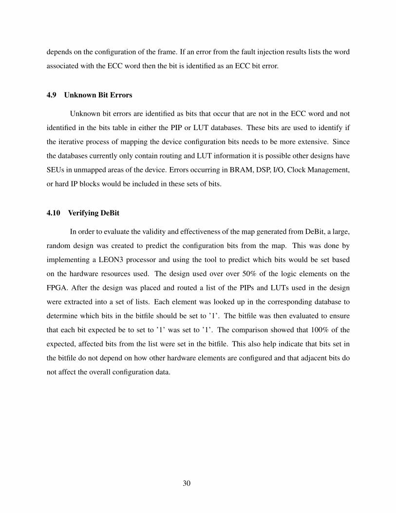
Table 5.1: Fault injection results of a B13 design using full TMR.
was recorded. If the error did not re-occur, the initial error was considered to be caused by an
accumulation of state errors from previously injected bits and not counted as an error.
After injecting 4,333,783 faults into the replicated B13 design 72 bits were found to pro-
duce errors. This results in an overall SEU sensitivity of 0.00166%. The classification results after
running the fault injection results through the DeBit tool are shown in Table 5.1. The results show
the most common failure type as clock bits. Clock bit failures are PIP junctions involving global
routing lines. Since no failures occurred in PIP junctions in non-global routes this indicated that
global routes had a unique failure mechanism.
Failures in PIP junctions specific to clock routing had not been identified in literature as
a failure mode for SEUs in TMR. Previous literature pointed to PIP junctions in causing shorts
and open circuits between nets in PIP junctions but had not distinction between global and regular
routes. Further analysis of the B13 errors also showed that the PIP junction causing an error shares
configuration bits between inputs to the PIP junction for regular nets as well as for at least two
clock nets from different domains.
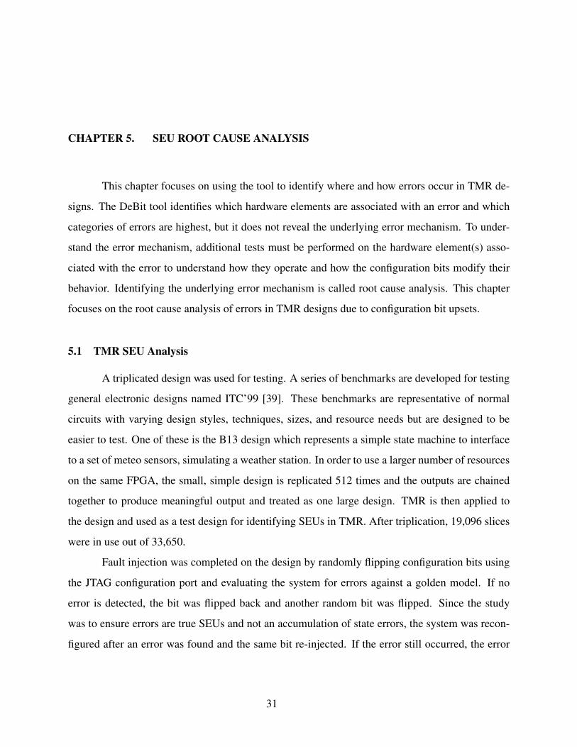
5.2 PIP Junction Analysis
In order to understand the root cause of the failure in PIP junctions a series of tests were
devised to more fully understand the PIP junction output under error conditions. The tests were
setup with two switches connected to two LEDs using various routing resources. The nets were
purposefully routed such that some of the PIP junctions between the two nets had inputs that could
source from the other net. This allowed for analysis of the behavior of one net while fault injecting
32
(a) Test platform.
(b) LED design running.
Figure 5.1: PIP Junction LED Test
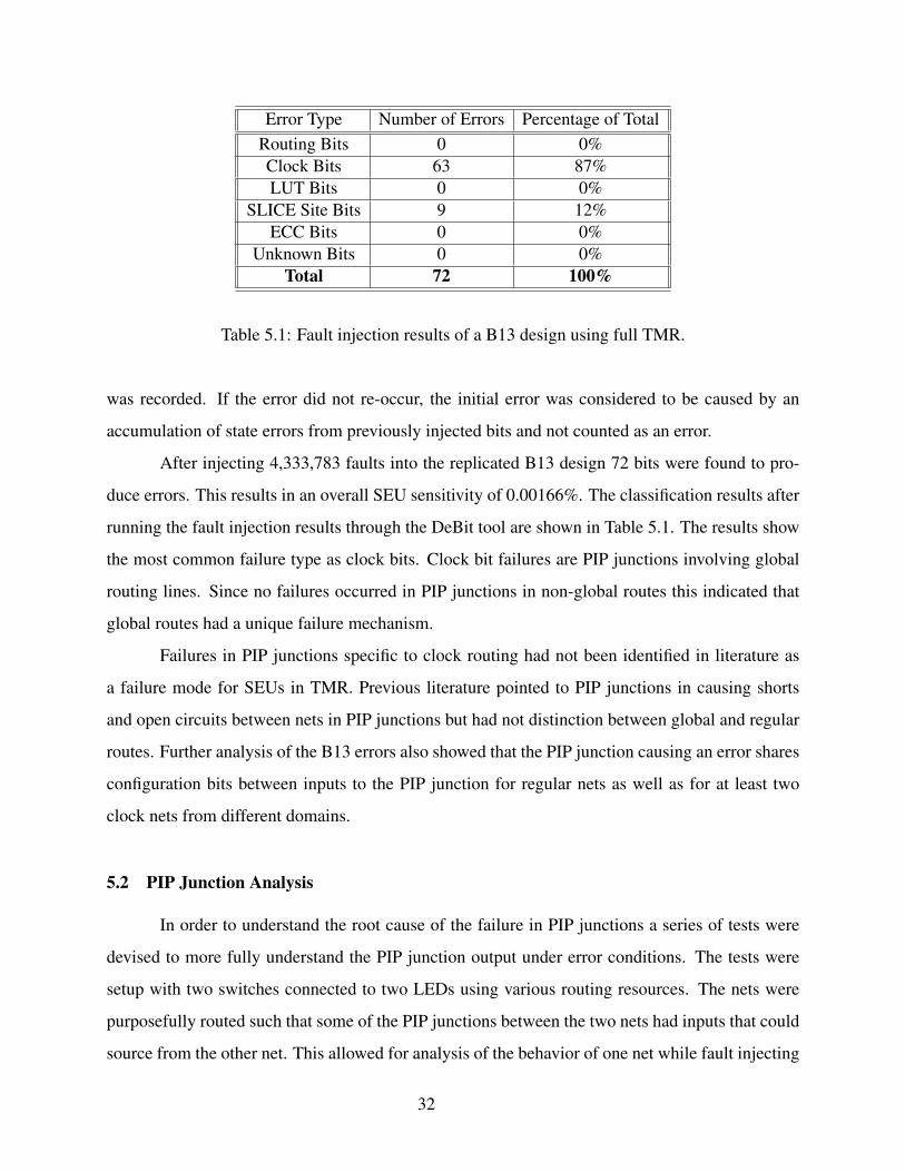
Figure 5.2: PIP junction failure analysis setup between two switches and two LEDs.
the other. The setup of each test is shown in Figure 5.1 where 5.1a shows the test platform and
5.1b shows one of the tests in operation. The different tests are detailed below.
5.3 PIP Junction Analysis: Regular Nets
The first setup was routed as shown in Figure 5.2 where two switches were connected
directly to two LEDs. The routing used regular, non-global nets. The design was routed in such a
way that the net between switch 0 and LED 0 could have used a PIP junction in the net along the
33
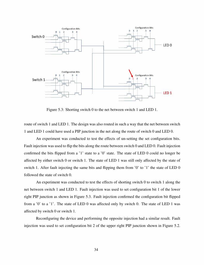
Figure 5.3: Shorting switch 0 to the net between switch 1 and LED 1.
route of switch 1 and LED 1. The design was also routed in such a way that the net between switch
1 and LED 1 could have used a PIP junction in the net along the route of switch 0 and LED 0.
An experiment was conducted to test the effects of un-setting the set configuration bits.
Fault injection was used to flip the bits along the route between switch 0 and LED 0. Fault injection
confirmed the bits flipped from a ’1’ state to a ’0’ state. The state of LED 0 could no longer be
affected by either switch 0 or switch 1. The state of LED 1 was still only affected by the state of
switch 1. After fault injecting the same bits and flipping them from ’0’ to ’1’ the state of LED 0
followed the state of switch 0.
An experiment was conducted to test the effects of shorting switch 0 to switch 1 along the
net between switch 1 and LED 1. Fault injection was used to set configuration bit 1 of the lower
right PIP junction as shown in Figure 5.3. Fault injection confirmed the configuration bit flipped
from a ’0’ to a ’1’. The state of LED 0 was affected only by switch 0. The state of LED 1 was
affected by switch 0 or switch 1.
Reconfiguring the device and performing the opposite injection had a similar result. Fault
injection was used to set configuration bit 2 of the upper right PIP junction shown in Figure 5.2.
34
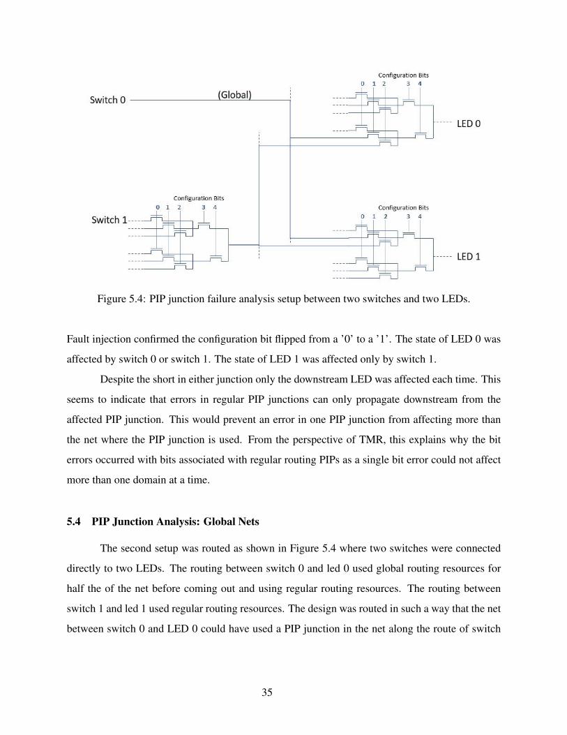
Figure 5.4: PIP junction failure analysis setup between two switches and two LEDs.
Fault injection confirmed the configuration bit flipped from a ’0’ to a ’1’. The state of LED 0 was
affected by switch 0 or switch 1. The state of LED 1 was affected only by switch 1.
Despite the short in either junction only the downstream LED was affected each time. This
seems to indicate that errors in regular PIP junctions can only propagate downstream from the
affected PIP junction. This would prevent an error in one PIP junction from affecting more than
the net where the PIP junction is used. From the perspective of TMR, this explains why the bit
errors occurred with bits associated with regular routing PIPs as a single bit error could not affect
more than one domain at a time.
5.4 PIP Junction Analysis: Global Nets
The second setup was routed as shown in Figure 5.4 where two switches were connected
directly to two LEDs. The routing between switch 0 and led 0 used global routing resources for
half the of the net before coming out and using regular routing resources. The routing between
switch 1 and led 1 used regular routing resources. The design was routed in such a way that the net
between switch 0 and LED 0 could have used a PIP junction in the net along the route of switch
35
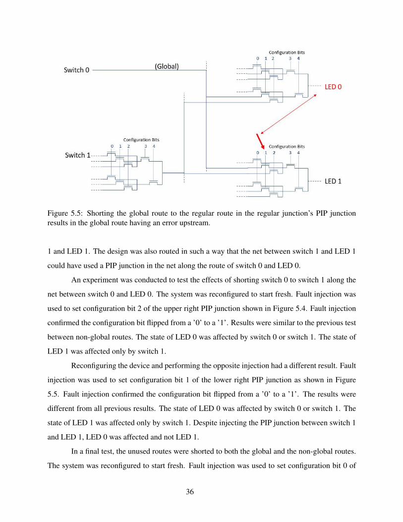
Figure 5.5: Shorting the global route to the regular route in the regular junction’s PIP junction
results in the global route having an error upstream.
1 and LED 1. The design was also routed in such a way that the net between switch 1 and LED 1
could have used a PIP junction in the net along the route of switch 0 and LED 0.
An experiment was conducted to test the effects of shorting switch 0 to switch 1 along the
net between switch 0 and LED 0. The system was reconfigured to start fresh. Fault injection was
used to set configuration bit 2 of the upper right PIP junction shown in Figure 5.4. Fault injection
confirmed the configuration bit flipped from a ’0’ to a ’1’. Results were similar to the previous test
between non-global routes. The state of LED 0 was affected by switch 0 or switch 1. The state of
LED 1 was affected only by switch 1.
Reconfiguring the device and performing the opposite injection had a different result. Fault
injection was used to set configuration bit 1 of the lower right PIP junction as shown in Figure
5.5. Fault injection confirmed the configuration bit flipped from a ’0’ to a ’1’. The results were
different from all previous results. The state of LED 0 was affected by switch 0 or switch 1. The
state of LED 1 was affected only by switch 1. Despite injecting the PIP junction between switch 1
and LED 1, LED 0 was affected and not LED 1.
In a final test, the unused routes were shorted to both the global and the non-global routes.
The system was reconfigured to start fresh. Fault injection was used to set configuration bit 0 of
36
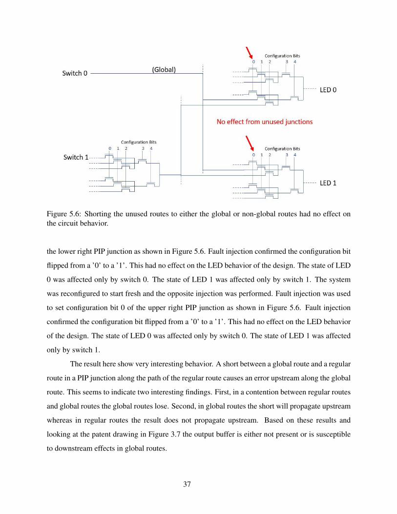
Figure 5.6: Shorting the unused routes to either the global or non-global routes had no effect on
the circuit behavior.
the lower right PIP junction as shown in Figure 5.6. Fault injection confirmed the configuration bit
flipped from a ’0’ to a ’1’. This had no effect on the LED behavior of the design. The state of LED
0 was affected only by switch 0. The state of LED 1 was affected only by switch 1. The system
was reconfigured to start fresh and the opposite injection was performed. Fault injection was used
to set configuration bit 0 of the upper right PIP junction as shown in Figure 5.6. Fault injection
confirmed the configuration bit flipped from a ’0’ to a ’1’. This had no effect on the LED behavior
of the design. The state of LED 0 was affected only by switch 0. The state of LED 1 was affected
only by switch 1.
The result here show very interesting behavior. A short between a global route and a regular
route in a PIP junction along the path of the regular route causes an error upstream along the global
route. This seems to indicate two interesting findings. First, in a contention between regular routes
and global routes the global routes lose. Second, in global routes the short will propagate upstream
whereas in regular routes the result does not propagate upstream. Based on these results and
looking at the patent drawing in Figure 3.7 the output buffer is either not present or is susceptible
to downstream effects in global routes.
37
5.5 PIP Junction Analysis: Application to TMR
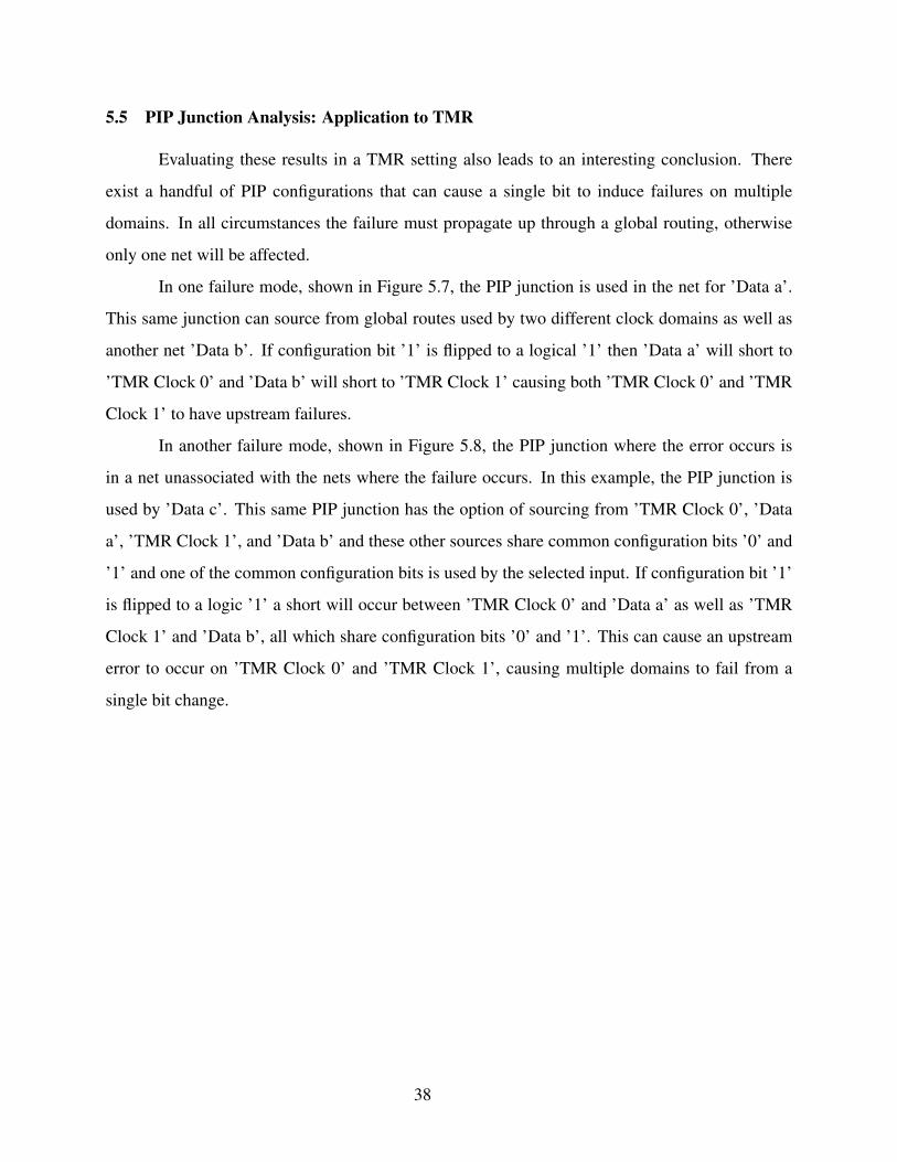
Evaluating these results in a TMR setting also leads to an interesting conclusion. There
exist a handful of PIP configurations that can cause a single bit to induce failures on multiple
domains. In all circumstances the failure must propagate up through a global routing, otherwise
only one net will be affected.
In one failure mode, shown in Figure 5.7, the PIP junction is used in the net for ’Data a’.
This same junction can source from global routes used by two different clock domains as well as
another net ’Data b’. If configuration bit ’1’ is flipped to a logical ’1’ then ’Data a’ will short to
’TMR Clock 0’ and ’Data b’ will short to ’TMR Clock 1’ causing both ’TMR Clock 0’ and ’TMR
Clock 1’ to have upstream failures.
In another failure mode, shown in Figure 5.8, the PIP junction where the error occurs is
in a net unassociated with the nets where the failure occurs. In this example, the PIP junction is
used by ’Data c’. This same PIP junction has the option of sourcing from ’TMR Clock 0’, ’Data
a’, ’TMR Clock 1’, and ’Data b’ and these other sources share common configuration bits ’0’ and
’1’ and one of the common configuration bits is used by the selected input. If configuration bit ’1’
is flipped to a logic ’1’ a short will occur between ’TMR Clock 0’ and ’Data a’ as well as ’TMR
Clock 1’ and ’Data b’, all which share configuration bits ’0’ and ’1’. This can cause an upstream
error to occur on ’TMR Clock 0’ and ’TMR Clock 1’, causing multiple domains to fail from a
single bit change.
38
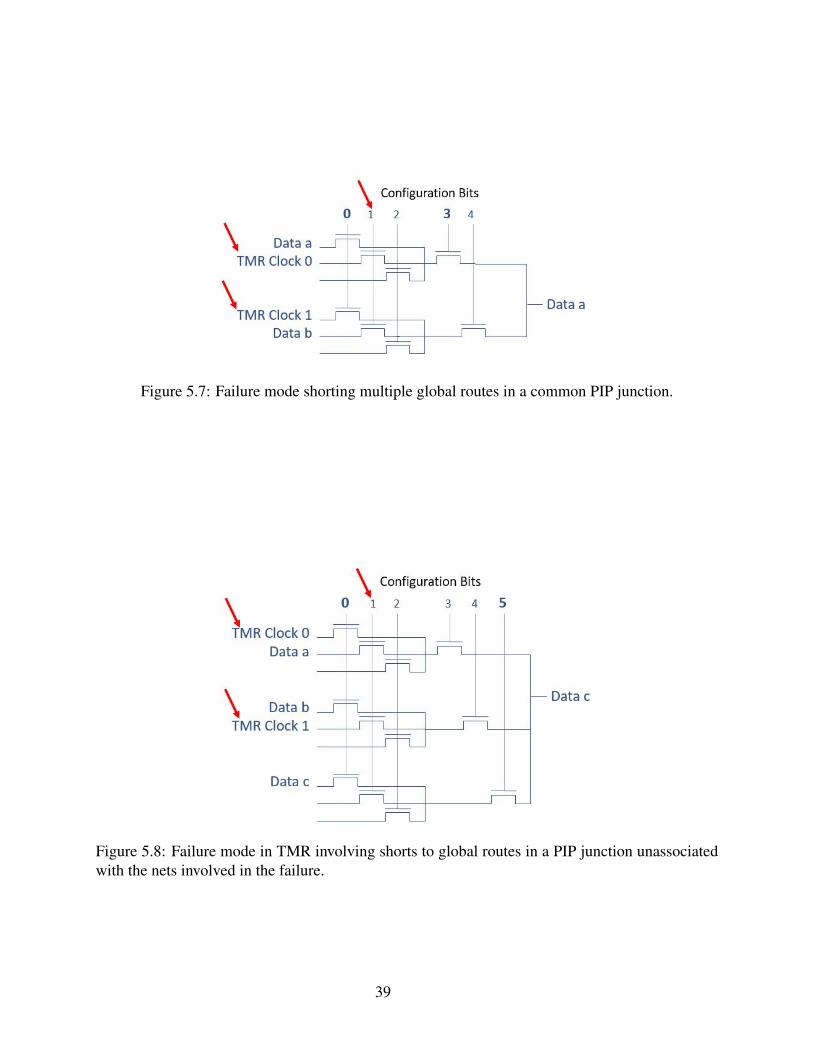
Figure 5.7: Failure mode shorting multiple global routes in a common PIP junction.
Figure 5.8: Failure mode in TMR involving shorts to global routes in a PIP junction unassociated
with the nets involved in the failure.
39
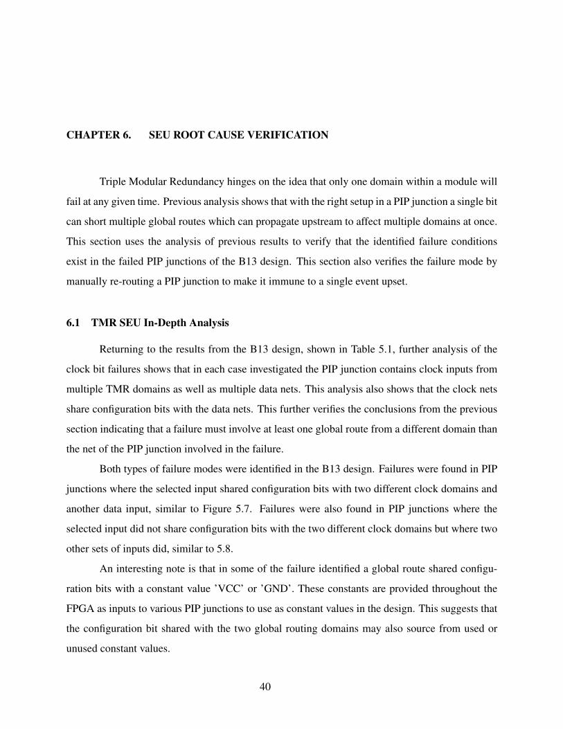
CHAPTER 6. SEU ROOT CAUSE VERIFICATION
Triple Modular Redundancy hinges on the idea that only one domain within a module will
fail at any given time. Previous analysis shows that with the right setup in a PIP junction a single bit
can short multiple global routes which can propagate upstream to affect multiple domains at once.
This section uses the analysis of previous results to verify that the identified failure conditions
exist in the failed PIP junctions of the B13 design. This section also verifies the failure mode by
manually re-routing a PIP junction to make it immune to a single event upset.
6.1 TMR SEU In-Depth Analysis
Returning to the results from the B13 design, shown in Table 5.1, further analysis of the
clock bit failures shows that in each case investigated the PIP junction contains clock inputs from
multiple TMR domains as well as multiple data nets. This analysis also shows that the clock nets
share configuration bits with the data nets. This further verifies the conclusions from the previous
section indicating that a failure must involve at least one global route from a different domain than
the net of the PIP junction involved in the failure.
Both types of failure modes were identified in the B13 design. Failures were found in PIP
junctions where the selected input shared configuration bits with two different clock domains and
another data input, similar to Figure 5.7. Failures were also found in PIP junctions where the
selected input did not share configuration bits with the two different clock domains but where two
other sets of inputs did, similar to 5.8.
An interesting note is that in some of the failure identified a global route shared configu-
ration bits with a constant value ’VCC’ or ’GND’. These constants are provided throughout the
FPGA as inputs to various PIP junctions to use as constant values in the design. This suggests that
the configuration bit shared with the two global routing domains may also source from used or
unused constant values.
40
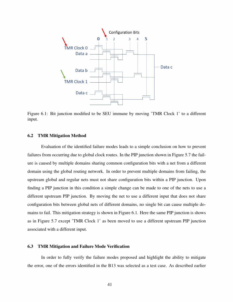
Figure 6.1: Bit junction modified to be SEU immune by moving ’TMR Clock 1’ to a different
input.
6.2 TMR Mitigation Method
Evaluation of the identified failure modes leads to a simple conclusion on how to prevent
failures from occurring due to global clock routes. In the PIP junction shown in Figure 5.7 the fail-
ure is caused by multiple domains sharing common configuration bits with a net from a different
domain using the global routing network. In order to prevent multiple domains from failing, the
upstream global and regular nets must not share configuration bits within a PIP junction. Upon
finding a PIP junction in this condition a simple change can be made to one of the nets to use a
different upstream PIP junction. By moving the net to use a different input that does not share
configuration bits between global nets of different domains, no single bit can cause multiple do-
mains to fail. This mitigation strategy is shown in Figure 6.1. Here the same PIP junction is shows
as in Figure 5.7 except ’TMR Clock 1’ as been moved to use a different upstream PIP junction
associated with a different input.
6.3 TMR Mitigation and Failure Mode Verification
In order to fully verify the failure modes proposed and highlight the ability to mitigate
the error, one of the errors identified in the B13 was selected as a test case. As described earlier
41
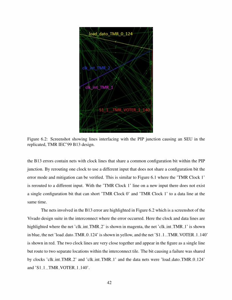
Figure 6.2: Screenshot showing lines interfacing with the PIP junction causing an SEU in the
replicated, TMR IEC’99 B13 design.
the B13 errors contain nets with clock lines that share a common configuration bit within the PIP
junction. By rerouting one clock to use a different input that does not share a configuration bit the
error mode and mitigation can be verified. This is similar to Figure 6.1 where the ’TMR Clock 1’
is rerouted to a different input. With the ’TMR Clock 1’ line on a new input there does not exist
a single configuration bit that can short ’TMR Clock 0’ and ’TMR Clock 1’ to a data line at the
same time.
The nets involved in the B13 error are highlighted in Figure 6.2 which is a screenshot of the
Vivado design suite in the interconnect where the error occurred. Here the clock and data lines are
highlighted where the net ’clk int TMR 2’ is shown in magenta, the net ’clk int TMR 1’ is shown
in blue, the net ’load dato TMR 0 124’ is shown in yellow, and the net ’S1 1 TMR VOTER 1 140’
is shown in red. The two clock lines are very close together and appear in the figure as a single line
but route to two separate locations within the interconnect tile. The bit causing a failure was shared
by clocks ’clk int TMR 2’ and ’clk int TMR 1’ and the data nets were ’load dato TMR 0 124’
and ’S1 1 TMR VOTER 1 140’.
42
To mitigate the error one of the clock lines was rerouted by hand into the same junction
from a different input, similar to Figure 6.1. The PIP and the tile were both exhaustively fault
injected to further show that the failure could no longer occur.
By routing into the same junction this verifies that the presence of two clock lines and
two data lines in the same PIP junction are not the dependent factor in the failure but, instead,
that the shared configuration bit between them creates the dependency. This finding allows PIP
junctions to share nets from different TMR domains as long as care is taken to avoid inputs that
share configuration bits. This requires the knowledge of which configuration bits are associated
with which hardware resource.
Since routing by hand through a design is a tedious and time consuming task future work
could benefit by automating the process of evaluating PIPs for error conditions and automatically
re-routing nets. Creating an automatic router is beyond the scope of this thesis but the results of
the experiments outlined herein have fed into the creation of an automatic router as well as a clever
placement methodology to use the vendor routing tools [40].
43
CHAPTER 7. CONCLUSION
An important step to identifying errors in TMR designs comes from understanding the un-
derlying hardware associated with a bit failure. The DeBit tool uncovered the underlying hardware
by mapping configuration bit errors to hardware resources. This allowed for faults to be catego-
rized according to the hardware affected by the bit error. By categorizing the errors based on the
hardware resources involved it was plain to see that the majority of errors in the B13 TMR design
were occurring due to global routing resources.
Another important step to understanding SEUs in TMR came from understanding the PIP
junction behavior under fault conditions. The series of simplified experiments comparing regular
routes to global routes revealed a unique failure mode for global routes compared to regular routes
and unused routes. This lead to identifying a novel failure mode for TMR designs where global
routes who share a configuration bit could be shorted to non-global routes sharing another con-
figuration bit. It was also identified that this failure could occur in a PIP junction along a route
unassociated with the global and non-global inputs in conflict.
The novel failure mode was verified by returning to the original B13 TMR design and
evaluating the PIP junctions associated with the SEUs. This verified the failure conditions existed
in those junctions and also identified that the same failures could occur with global routes being
shorted to constant values of ’VCC’ and ’GND’ in place of regular nets. This failure mode was
further verified by re-routing a global route in a failed junction to use a different input in the same
junction and exhaustively fault injecting the tile without error. The successful outcome of the test
helps solidify the novel failure mode as well as propose a potential method for identifying SEUs
and mitigating them on existing designs.
It is hoped this understanding can help devise methods of improving TMR against SEUs.
Vendor tools are not currently set up to be aware of different TMR domains during routing to
prevent PIP junction and slice SEUs. For PIP junctions, automated tools can be developed to auto-
44
matically consider the bits associated with a PIP junction and neighboring inputs before choosing
a route or before creating a bitfile. Reliability gains can be achieved by modifying placement and
routing tools to allow the user to tag design elements as needing to remain SEU separated from
one another. For sites with site-wide bit modifications, additional reliability can be achieved by
being aware of the TMR domains during slice resource allocation. By understanding the failure
mechanisms behind SEUs better tools can be created to improve FPGA reliability in high radiation
environments without going through costly design changes to the FPGA’s underlying hardware.
FPGA markets are expected to grow in coming years and, consequently, the need for reliable FPGA
designs is likely to increase as well. The hope is this work will continue to push that improvement
forward.
45
REFERENCES
[1] Baumann, R. C., 2005. “Radiation-induced soft errors in advanced semiconductor technolo-
gies.” IEEE Transactions on Device and Materials Reliability, 5(3), pp. 305–316. vii, 4,
5
[2] Young, S., Tanikella, R., and Stokes, S., 2007. Integrated circuit interconnect structure having
reduced coupling between interconnect lines, Apr. 3 US Patent 7,199,610. vii, 16
[3] Xilinx, 2016. 7 series FPGAs configurable logic block user guide (ug474), 9. vii, 20
[4] Intel, 2020. “Intel Stratix 10 GX/SX device overview (s10-overview).”. 1
[5] Morris, K., 2019. “Intel’s world’s largest FPGA.” EEJournal, 12. 1
[6] Wallmark, J. T., and Marcus, S. M., 1962. “Minimum size and maximum packing density of
nonredundant semiconductor devices.” Proceedings of the IRE, 50(3), March, pp. 286–298.
1, 4
[7] Katz, R., LaBel, K., Wang, J., Cronquist, B., Koga, R., Penzin, S., and Swift, G., 1997. “Ra-
diation effects on current field programmable technologies.” IEEE Transactions on Nuclear
Science, 44(6), pp. 1945–1956. 1, 5
[8] Wang, J. J., Katz, R. B., Sun, J. S., Cronquist, B. E., McCollum, J. L., Speers, T. M., and
Plants, W. C., 1999. “Sram based re-programmable FPGA for space applications.” IEEE
Transactions on Nuclear Science, 46(6), Dec, pp. 1728–1735. 1, 2
[9] Ceschia, M., Bellato, M., Paccagnella, A., and Kaminski, A., 2002. “Ion beam testing of
Altera Apex FPGAs.” pp. 45–50. 1, 5
[10] Bellato, M., Bernardi, P., Bortolato, D., Candelori, A., Ceschia, M., Paccagnella, A., Rebau-
dengo, M., Reorda, M. S., Violante, M., and Zambolin, P., 2004. “Evaluating the effects of
SEUs affecting the configuration memory of an SRAM-based FPGA.” pp. 584–589. 1, 5
[11] Quinn, H., Graham, P., Krone, J., Caffrey, M., and Rezgui, S., 2005. “Radiation-induced
multi-bit upsets in SRAM-based FPGAs.” IEEE Transactions on Nuclear Science, 52(6),
pp. 2455–2461. 1, 6
[12] Velazco, R., Foucard, G., and Peronnard, P., 2010. “Combining results of accelerated ra-
diation tests and fault injections to predict the error rate of an application implemented in
SRAM-based FPGAs.” IEEE Transactions on Nuclear Science, 57(6), pp. 3500–3505. 1, 6
[13] Ma, T.-P., and Dressendorfer, P. V., 1989. Ionizing radiation effects in MOS devices and
circuits. John Wiley & Sons. 1, 5
46
[14] Xilinx, 2018. “7 series FPGAs configuration (ug470).”. 2, 21
[15] Xilinx, 2020. “Solution brief.” Aerospace Defence. 2
[16] Fuller, E., and Caffrey, M., 2000. Radiation testing update, SEU mitigation, and availability
analysis of the Virtex FPGA for space reconfigurable computing. Tech. rep., Los Alamos
National Lab., Los Alamos, NM (US). 2, 7, 8
[17] Adell, P., Allen, G., Swift, G., and McClure, S., 2008. “Assessing and mitigating radiation
effects in Xilinx SRAM FPGAs.” pp. 418–424. 2
[18] Xilinx, 2018. “Radiation-hardened, space-grade Virtex-5QV family data sheet: Overview
(ds192).”. 2
[19] Sterpone, L., and Violante, M., 2006. “A new reliability-oriented place and route algorithm
for SRAM-based FPGAs.” IEEE Transactions on Computers, 55(6), June, pp. 732–744. 3, 9
[20] Sterpone, L., and Violante, M., 2005. “A new analytical approach to estimate the effects of
SEUs in TMR architectures implemented through SRAM-based FPGAs.” IEEE Transactions
on Nuclear Science, 52(6), Dec, pp. 2217–2223. 3, 9
[21] Baumann, R. C., 2005. “Radiation-induced soft errors in advanced semiconductor technolo-
gies.” IEEE Transactions on Device and Materials Reliability, 5(3), pp. 305–316. 4
[22] Barth, J. L., Dyer, C., and Stassinopoulos, E., 2003. “Space, atmospheric, and terrestrial
radiation environments.” IEEE Transactions on nuclear science, 50(3), pp. 466–482. 5
[23] Sterpone, L., and Violante, M., 2007. “A new partial reconfiguration-based fault-injection
system to evaluate SEU effects in SRAM-based FPGAs.” IEEE Transactions on Nuclear
Science, 54(4), pp. 965–970. 6
[24] Lima, F., Carmichael, C., Fabula, J., Padovani, R., and Reis, R., 2001. “A fault injection
analysis of Virtex FPGA TMR design methodology.” pp. 275–282. 6
[25] Carmichael, C., 2001. “Correcting single-event upsets through Virtex partial configuration.”
Xilinx Application Notes, 197, p. v1. 7
[26] Harding, A., and Wirthlin, M., 2014. “Improving the reliability of Xilinx 7 series FPGAs
through configuration scrubbing.”. 7
[27] Stoddard, A., Gruwell, A., Zabriskie, P., and Wirthlin, M. J., 2017. “A hybrid approach to
FPGA configuration scrubbing.” IEEE Transactions on Nuclear Science, 64(1), pp. 497–503.
7
[28] Stoddard, A., Gruwell, A., Zabriskie, P., and Wirthlin, M., 2016. “High-speed PCAP config-
uration scrubbing on Zynq-7000 all programmable SoCs.” pp. 1–8. 7
[29] Legat, U., Biasizzo, A., and Novak, F., 2012. “SEU recovery mechanism for SRAM-based
FPGAs.” IEEE Transactions on Nuclear Science, 59(5), pp. 2562–2571. 7
47
[30] Herrera-Alzu, I., and Lopez-Vallejo, M., 2013. “Design techniques for Xilinx Virtex FPGA
configuration memory scrubbers.” IEEE Transactions on Nuclear Science, 60(1), pp. 376–
385. 7
[31] Lyons, R. E., and Vanderkulk, W., 1962. “The use of triple-modular redundancy to improve
computer reliability.” IBM Journal of Research and Development, 6(2), April, pp. 200–209.
7, 8
[32] Arifeen, T., Hassan, A. S., and Lee, J., 2020. “Approximate triple modular redundancy: A
survey.” IEEE Access, 8, pp. 139851–139867. 7
[33] Xilinx, 2019. “Microblaze triple modular redundancy (TMR) subsystem v1.0.” Xilinx Prod-
uct Guide, PG268, p. v1. 7
[34] Samudrala, P. K., Ramos, J., and Katkoori, S., 2004. “Selective triple modular redundancy
(STMR) based single-event upset (SEU) tolerant synthesis for FPGAs.” IEEE Transactions
on Nuclear Science, 51(5), pp. 2957–2969. 7
[35] Chattopadhyay, S., Tripathi, S. B., Goswami, M., and Sen, B., 2016. “Design of fault tolerant
majority voter for TMR circuit in QCA.” pp. 1–2. 7
[36] Bernardi, P., Reorda, M. S., Sterpone, L., and Violante, M., 2004. “On the evaluation of SEU
sensitiveness in SRAM-based FPGAs.” pp. 115–120. 8
[37] Ceschia, M., Violante, M., Reorda, M. S., Paccagnella, A., Bernardi, P., Rebaudengo, M.,
Bortolato, D., Bellato, M., Zambolin, P., and Candelori, A., 2003. “Identification and classi-
fication of single-event upsets in the configuration memory of SRAM-based FPGAs.” IEEE
Transactions on Nuclear Science, 50(6), Dec, pp. 2088–2094. 8
[38] Xilinx, 2018. 7 series FPGAs clocking resources (ug472), 7. 11
[39] Corno, F., Reorda, M. S., and Squillero, G., 2000. “RT-level ITC’99 benchmarks and first
ATPG results.” IEEE Design Test of Computers, 17(3), pp. 44–53. 31
[40] Cannon, M., Keller, A., and Wirthlin, M., 2018. “Improving the effectiveness of TMR designs
on FPGAs with SEU-aware incremental placement.” pp. 141–148. 43
48

APPENDIX A. TILE TYPES OF THE VIRTEX 7 ARCHITECTURE
• B TERM INT
• BRAM INT INTERFACE L
• BRAM INT INTERFACE R
• BRAM L
• BRAM R
• BRKH B TERM INT
• BRKH BRAM
• BRKH CLB
• BRKH CLK
• BRKH CMT
• BRKH DSP L
• BRKH DSP R
• BRKH INT
• BRKH TERM INT
• CFG CENTER BOT
• CFG CENTER MID
• CFG CENTER TOP
49

• CLBLL L
• CLBLL R
• CLBLM L
• CLBLM R
• CLK BUFG BOT R
• CLK BUFG REBUF
• CLK BUFG TOP R
• CLK FEED
• CLK HROW BOT R
• CLK HROW TOP R
• CLK MTBF2
• CLK PMV
• CLK PMV2 SVT
• CLK PMV2
• CLK PMVIOB
• CLK TERM
• CMT FIFO L
• CMT FIFO R
• CMT PMV L
• CMT PMV
• CMT TOP L LOWER B
50
• CMT TOP L LOWER T
• CMT TOP L UPPER B
• CMT TOP L UPPER T
• CMT TOP R LOWER B
• CMT TOP R LOWER T
• CMT TOP R UPPER B
• CMT TOP R UPPER T
• DSP L
• DSP R
• GTP CHANNEL 0 MID LEFT
• GTP CHANNEL 0 MID RIGHT
• GTP CHANNEL 1 MID LEFT
• GTP CHANNEL 1 MID RIGHT
• GTP CHANNEL 2 MID LEFT
• GTP CHANNEL 2 MID RIGHT
• GTP CHANNEL 3 MID LEFT
• GTP CHANNEL 3 MID RIGHT
• GTP COMMON MID LEFT
• GTP COMMON MID RIGHT
• GTP INT INT TERM L
• GTP INT INT TERM R
51

• GTP INT INTERFACE L
• GTP INT INTERFACE R
• GTP MID CHANNEL STUB
• GTP MID COMMON STUB
• HCLK BRAM
• HCLK CLB
• HCLK CMT L
• HCLK CMT
• HCLK DSP L
• HCLK DSP R
• HCLK FEEDTHRU 1
• HCLK FEEDTHRU 2
• HCLK FIFO L
• HCLK INT INTERFACE
• HCLK IOB
• HCLK IOI3
• HCLK L BOT UTURN
• HCLK L
• HCLK R BOT UTURN
• HCLK R
• HCLK TERM
52

• HCLK VBRK
• HCLK VFRAME
• INT FEEDTHRU 1
• INT FEEDTHRU 2
• INT INTERFACE L
• INT INTERFACE R
• INT L
• INT R
• IO INT INTERFACE L
• IO INT INTERFACE R
• L TERM INT
• LIOB33 SING
• LIOB33
• LIOI3 SING
• LIOI3 TBYTESRC
• LIOI3 TBYTETERM
• LIOI3
• MONITOR BOT
• MONITOR MID
• MONITOR TOP
• PCIE BOT
53

• PCIE INT INTERFACE L
• PCIE INT INTERFACE R
• PCIE TOP
• R TERM INT
• RIOB33 SING
• RIOB33
• RIOI3 SING
• RIOI3 TBYTESRC
• RIOI3 TBYTETERM
• RIOI3
• T TERM INT
• TERM CMT
• VBRK
• VFRAME
54