rom-7420 risc on module -...
TRANSCRIPT

Qseven RISC Carrier Board Design Guide
ROM-7420
RISC On Module
Carrier Board Design Guide
Version 1.0

Qseven RISC Carrier Board Design Guide
Notices
The copyright on this user manual remains with Advantech Co., Ltd. No part of this
user manual may be transmitted, reproduced, or changed.
Other companies’ product names that may be used herein remain the property of their
respective owners.
The product specifications, design and this user’s manuals content are subject to
change without notice.
If you have any questions, please contact your merchant or our service center for
clarification. We are not responsible for any losses resulting from using this product
no matter what the reason.
Revision History
Version/Revisione Date Dat Description
Version 1.0 May, 2013 Initial release
Part No. Edition 1.0
Printed in Taiwan May, 2013

Qseven RISC Carrier Board Design Guide

Qseven RISC Carrier Board Design Guide
Chapter 1 Introduction
This design guide is created for ROM-7420 RISC extension module by
Advantech. This document describes the key features and function block as
well as the mechanical and electrical characteristics on ROM-7420 to help
users who want to develop their own carrier board with the module.
1.1 RISC On Module (ROM) Structures
Advantech provides next generation performance of the smallest state of the art
embedded modules. With a scalable solution that meets customer's advanced CPU
application development needs and reduces time-to-market. Advantech’s business
offered helps customers develop custom CPU board solutions extremely fast and with
lower investment. Using ROM-DTOS, customers can reduce traditional customized
CPU board development time and costs by as much as 80%. Advantech offers a wide
range of industrial standard interfaces on ROM product to cater to each customer's
demands. The modular designs allow upgrade ability and add more flexibility to the
system. The form factor allows the ROM module to be easily and securely mounted
on a customized solution board. The design and well verified platform eliminate CPU
integration worries and allow fast application support for the most dynamic embedded
needs.
ROM is a series of reliable and widely used ARM’s CPU cores with high integration
features. ROM-7420 supports wide range of accessibility to reach the latest technical
trend such like SDHC and USB 2.0. Not only does ROM allow quick design, it also
provides the benefits of easy installation, maintenance and upgrade.

Qseven RISC Carrier Board Design Guide
Though small in size, ROM takes care of most complicated CPU architectures and
basic common circuits. Many system integrators are finding an Advantech ROM
solution already covers 80% of their feature requirements. This makes ROM a
powerful time and money saver.
ROM + Customer Solution Board = Your Customized Platform. RISC On Modules
save time and money. Using ROM-DTOS allows customers to realize cost savings
and most importantly, faster time to market, two keys to help ensure your product’s
success in the market.

Qseven RISC Carrier Board Design Guide
1.2 Terminology Table 1.1 Conventions and Terminology
CODEC COMPRESSOR and DECOMPRESSOR CPU Central processing Unit
CRT Cathode Ray Tube
DDR Double Data Rate SDRAM memory technology
SRAM Static Random Access Memory
GPMC General Purpose Memory Controller
GPIO General Purpose Input Output
EMI Electromagnetic Interference
ESR Equivalent Series Resistance
ESD Electrostatic Discharge
I2C Inter-IC (a two wire serial bus created by Philips)
IrDA Infrared Data Association
LCD Liquid Crystal Display
LVDS Low Voltage Differential Signaling: A high speed, low power data
transmission standard used for display connections to LCD panels.
NTSC National Television Standards Committee
PAL Phase Alternate Line
RTC Real Time Clock
ROM RISC On Module CSB Customer Solution Board
PCB Printed Circuit Board
USB Universal Serial Bus
UART Universal Asynchronous Receiver/Transmitter
DAC Digital Analog Converter
N/C Not Connected
N/A Not Applied in this case
NL/ No Load (do not populate this part on PCB)
SDHC Secure Digital High Capacity
DSP Digital Signal Processing
RISC Reduced Instruction Set Computing
EEPROM Electrically Erasable Programmable Read Only Memory
Kbps Kilo-bit per second
SPI bus Serial Peripheral Interface bus
mil Length unit, 1000 mils = 1 inch

Qseven RISC Carrier Board Design Guide
1.3 Specification of ROM-7420
Advantech’s new ROM-7420 is the ultimate powerful ROM module able to drive the
most demanding embedded applications requiring high performance CPU processing
power & graphics support. With support for Freescale® i.MX6 processor & enhanced
power-saving technology, the ROM-7420 offers developers a low power and
scaleable solution that fits a moderate range of needs. The processors feature
Freescale’s advanced implementation of the quad ARM Cortex™-A9 core, which
operates at speeds up to 1 GHz. Integrated 2D and 3D 1080p video processing
multimedia accelerator strengthened by internal Video Processing Unit (VPU) up
to1920 x 1080 x 30fps (1080P). The i.MX6 CPU supports up to 1GB addressing
space of 533MHz DDR3 DRAM (i.e. DDR3-1066) by means of 4 Chip-Select pin
architecture and 4Gbit memory size per chip-select pin. Data width of DDR3 memory
could be either 32-bit or 64-bit.
ROM-7420 Main Features:
• Embedded Freescale® i.MX6 processor
• Supports 1 host USB2.0 port and 1 USB OTG port
• Supports 1 SD/MMC/SDHC interfaces with 4-bit data pin
• Supports 1 10/100/1000 Fast Ethernet port
• Supports 2 CAN BUS ports
• Supports 1 SATA-II port
• Support 1 PCI-e Gen2 x1 port
• Support 1 HDMI 1.4 output
• Support 1 VGA output
• Support 8 GPIO ports
• Integrated 4GB EMMC NAND Flash
Qseven RISC Carrier Board Design Guide
• Be able to boot from external SD interface or from internal SPI flash memory
• Supports 2 independent ports single channel 24-bit LCD display interface up to
1080p @ 60fps data rate
Qseven RISC Carrier Board Design Guide
Chapter 2 Pin Assignments
There are 115 edge fingers on the top and bottom side of the Qseven™ module that
mate with the MXM connector. Table 2-1 lists the pin assignments for all 230 edge
fingers.
Table 2-1 Pin Assignments
Pin Signal Pin Signal
1 GND 2 GND
3 GBE_MDI3- 4 GBE_MDI2-
5 GBE_MDI3+ 6 GBE_MDI2+
7 GBE_LINK100# 8 GBE_LINK1000#
9 GBE_MDI1- 10 GBE_MDI0-
11 GBE_MDI1+ 12 GBE_MDI0+
13 N/A 14 GBE_ACT#
15 N/A 16 N/A
17 N/A 18 CB_PWR_EN
19 N/A 20 PWRBTN#
21 SLP_BTN# 22 N/A
23 GND 24 GND
Key Key
25 GND 26 PWGIN
27 N/A 28 RSTBTN#
29 SATA0_TX+ 30 N/A
31 SATA0_TX- 32 N/A
33 N/A 34 GND
35 SATA0_RX+ 36 N/A
37 SATA0_RX- 38 N/A
39 GND 40 GND
41 N/A 42 SDIO_CLK#
43 SDIO_CD# 44 N/A
45 SDIO_CMD 46 SDIO_WP
47 N/A 48 SDIO_DAT1
49 SDIO_DAT0 50 SDIO_DAT3
51 SDIO_DAT2 52 N/A
53 N/A 54 N/A
55 N/A 56 GF_DET1
57 GND 58 GND
59 I2S_CLK 60 N/A
61 I2S_WS 62 N/A
63 I2S_MCLK 64 N/A
65 I2S_SDO 66 I2C_CLK
67 I2S_SDI 68 I2C_DAT
69 N/A 70 WDTRIG#
71 N/A 72 N/A
73 GND 74 GND

Qseven RISC Carrier Board Design Guide
75 UART5_TX 76 UART4_TX
77 UART5_RX 78 UART4_RX
79 N/A 80 N/A
81 N/A 82 N/A
83 N/A 84 N/A
85 N/A 86 USB_0_1_OC#
87 N/A 88 USB_OTG_PEN
89 N/A 90 USB_OTG_VBUS
91 USB_CC 92 USB_ID
93 USB_P1- 94 USB_P0-
95 USB_P1+ 96 USB_P0+
97 GND 98 GND
99 LVDS_A0+ 100 LVDS_B0+
101 LVDS_A0- 102 LVDS_B0-
103 LVDS_A1+ 104 LVDS_B1+
105 LVDS_A1- 106 LVDS_B1-
107 LVDS_A2+ 108 LVDS_B2+
109 LVDS_A2- 110 LVDS_B2-
111 LVDS_PPEN 112 LVDS_BLEN
113 LVDS_A3+ 114 LVDS_B3+
115 LVDS_A3- 116 LVDS_B3-
117 GND 118 GND
119 LVDS_A_CLK+ 120 LVDS_B_CLK+
121 LVDS_A_CLK- 122 LVDS_B_CLK-
123 GP_PWM_OUT0 124 GF_DET2
125 GP_I2C_DAT
I2C1_DAT
126 LVDS_BLC_DAT
I2C2_DAT 127 GP_I2C_CLK
I2C1_CLK
128 LVDS_BLC_CLK
I2C2_CLK 129 CAN0_TX 130 CAN0_RX
131 TMDS_CLK+ 132 UART2_TX
133 TMDS_CLK- 134 UART2_RX
135 GND 136 GND
137 TMDS_LANE1+ 138 UART3_TX
139 TMDS_LANE1- 140 UART3_RX
141 GND 142 GND
143 TMDS_LANE0+ 144 CAN1_TX
145 TMDS_LANE0- 146 CAN1_RX
147 GND 148 GND
149 TMDS_LANE2+ 150 HDMI_CTRL_DAT
I2C2_DAT 151 TMDS_LANE2- 152 HDMI_CTRL_CLK
I2C2_CLK 153 HDMI_HPD# 154 N/A
155 PCIE_CLK_REF+ 156 PCIE_WAKE#
157 PCIE_CLK_REF- 158 PCIE_RST#
159 GND 160 GND
161 GPIO_4 162 GPIO_0
163 GPIO_5 164 GPIO_1
165 GND 166 GND
167 GPIO_6 168 GPIO_2
169 GPIO_7 170 GPIO_3
Qseven RISC Carrier Board Design Guide
171 N/A 172 N/A
173 N/A 174 N/A
175 N/A 176 N/A
177 N/A 178 PCIE_DIS#
179 PCIE0_TX+ 180 PCIE0_RX+
181 PCIE0_TX- 182 PCIE0_RX-
183 GND 184 GND
185 VGA0_RED 186 VGA_I2C_CK
187 VGA0_GRN 188 VGA_I2C_DAT
189 VGA0_BLU 190 VGA_VSYNC
191 N/A 192 VGA_HSYNC
193 VCC_RTC 194 N/A
195 N/A 196 N/A
197 GND 198 GND
199 SPI_MOSI 200 SPI_CS0
201 SPI_MISO 202 SPI_CS1
203 SPI_SCK 204 JTAG_TRST#
205 N/A 206 N/A
207 JTAG_TCK 208 JTAG_TDI
209 JTAG_TDO 210 JTAG_TMS
211 VCC 212 VCC
213 VCC 214 VCC
215 VCC 216 VCC
217 VCC 218 VCC
219 VCC 220 VCC
221 VCC 222 VCC
223 VCC 224 VCC
225 VCC 226 VCC
227 VCC 228 VCC
229 VCC 230 VCC

Qseven RISC Carrier Board Design Guide

Qseven RISC Carrier Board Design Guide

Qseven RISC Carrier Board Design Guide
Chapter 3 Carrier Board Design Guidelines
3.1 Ethernet
ROM-7420 supports the IEEE802.3 network interface and flexible dynamically
loadable EEPROM algorithm. The network interface complies with the IEEE standard
for 10BASE-T, 100BASE-T and 1000BASE-T Ethernet interfaces.
3.1.1 Signal Descriptions
Table 3-1 shows ROM-7420 Ethernet signals, including pin number, signal
naming, I/O, and descriptions.
Table 3-1 GBE signals
Signal Pin I/O Description
GBE_MDI[0:3]+
GBE_MDI[0:3]-
3,4,5,6,
9,10,11,
12
I/O Media Dependent Interface (MDI) differential pair 0~3
The MDI can operate in 1000, 100, and 10Mbit/sec
modes. This signal pair is used for all modes.
GBE_ACT# 14 OD Gigabit Ethernet Controller 0 activity indicator, active
low.
GBE_LINK100# 7 OD Gigabit Ethernet Controller 0 100 Mbit / sec link indictor,
active low.
GBE_LINK1000# 8 OD Gigabit Ethernet Controller 0 1000 Mbit / sec link
indictor, active low.
3.1.2 Schematic Guidelines
3.1.2.1 Differential Pairs
Designing for Gigabit Ethernet operation is very similar to the designing for 10/100
Mbps. 10/100Mbps Ethernet has two differential pairs, and Gigabit Ethernet has four
differential pairs. Figure 3-1 and Figure 3-2 show the 10/100M Ethernet and Gigabit
Ethernet Connections.

Qseven RISC Carrier Board Design Guide
Figure
3-1 10/100M Ethernet Connections
Figure 3-2 Gigabit Ethernet Connections
3.1.2.2 LAN Connector with Integrated Magnetic
For simplifying the schematic and layout considerations of LAN connector, it is
strongly recommended to use the RJ45 LAN connector. Figure 3-3 shows the
integrated magnetic schematic.

Qseven RISC Carrier Board Design Guide
Figure 3-3 Gigabit Ethernet Connections with Integrated Magnetic
3.1.2.3 Implementation of Ethernet LED indicators
RJ-45 connector with LED indicators needs 3.3V to drive the LEDs. The Link and
activity LEDs can be implemented by using the ROM-7420 Module’s GBE_ACT#,
GBE_LINK100#, and GBE_LINK1000# pins. The sink current is connected to the
cathode of the LED, and the anode of the LED should be pulled to
3.3V through a resistor as 330 Ω.
3.1.3 Layout Guidelines
Route the transmit and receive lines on the carrier board as differential pairs, with a
differential impedance of 100 Ω. PCB layout software allows determination of the
proper trace width and spacing to achieve the impedance after the PCB stack-up
configuration.
The TX+/TX- signal pair should be well separated from the RX+/RX- signal pair. Both
pairs should be well separated from any other signals on the PCB. The total routing
length of these pairs from the ROM-7420 Module to the Ethernet RJ45 connector
should be made as short as practical.
For Ethernet connector placement, place it as close as possible to the ROM-7420

Qseven RISC Carrier Board Design Guide
Module pins to shorten the routing lengths of all Ethernet signals. Differential signal
traces should be kept as short as possible to decrease the possibility of being
affected by high frequency noise from other signals and power planes, and capacitive
loading is also reduced. Please refer to the Advantech layout checklist for detail.
3.1.3.1 Differential pairs design considerations
Maintain constant symmetry and spacing between the traces within a differential
pair. Keep the signal trace lengths of a differential pair equal to each other. Do
not use serpentines to try to match trace lengths in the differential pair.Serpentines
cause impedance variations causing signal reflections, which can be a source of
signal distortion. Try to keep the length difference of the differential pair less than 5
mil.
● The total length of each differential pair should be less than 6.8 inches. Keep the
length of each differential pair under 6.8 inches. Figure 3-4 shows an example.
Please refer to the Advantech layout checklist for detailed length matching.
● Do not route the transmit differential traces closer than 50 mils to the receive
differential traces for 10/100 Mbps. Figure 3-4 shows an example. It’s recommended
to keep length L3 longer than 50 mils.
● Do not route any other signal traces (including other differential pairs) parallel to
the differential traces or closer than 20 mils. Figure 3-4 shows an example. It’s
recommended to keep length L3 longer than 50 mils to the differential traces.
.
● Keep separate traces within a differential pair as small as possible down to 5 to 8
Mils, depending on the impedance control. Close separation of the traces allow
the traces to couple well to each other.
● For high-speed signals, they should minimize the number of corners and vias. If a
90° bend is required, it is recommended to use two 45° bends instead. Figure 3-5
shows the example.

Qseven RISC Carrier Board Design Guide
Figure 3-4 Differential signals route example
Figure 3-5 Bend layout example
3.1.3.2 Transformer
It’s recommended to use the integrated Magnetic Modules/RJ-45 LAN connectors. If
using the discrete Magnetic Modules and RJ-45 connector, the transformer should be
placed close to the RJ-45 LAN connector to reduce EMI emissions. Each differential
pair of data signals is required to be parallel to each other with the same trace length
on the component (top) layer and to be parallel to a respective ground plane.The
connector with integrated magnetic is much simplified for layout. The more complex
layout as Figure 3-6 and Figure 3-7 shows the 10/100M and Gigabit Ethernet layout
with discrete magnetic.

Qseven RISC Carrier Board Design Guide
Figure 3-6 10/100M Ethernet Interconnection
Figure 3-7 Gigabit Ethernet Interconnection

Qseven RISC Carrier Board Design Guide
3.1.3.3 Power Considerations
In general, any section of traces that is intended for use with high-speed signals
should observe proper termination practices. Many board layouts remove the ground
plane underneath the transformer and the RJ-45 connector to minimize capacitive
coupling of noise between the plane and the external Ethernet cable.
3.1.3.4 Critical Dimensions
There are two critical dimensions that must be considered during the layout phase of
an Ethernet controller. These dimensions are identified in Figure 3-8 as distance A
and B.
Distance A: Transformer to RJ-45 LAN Connector (Priority 1). The distance labeled A
should be given the highest priority in the backplane layout. The distance between
the transformer module and the RJ-45 connector should be kept to less than 1 inch
of separation. The following trace characteristics are important and should be
observed:
1. Differential Impedance: The differential impedance should be 100 Ω. The single
ended trace impedance will be approximately 50 Ω; however, the differential
impedance can also be affected by the spacing between the traces.
2. Trace Symmetry: Differential pairs should be routed with consistent separation
and with exactly the same lengths and physical dimensions (for example, width and
spacing).
Distance B: From ROM-7420 Module to Transformer (Priority 2). Distance B should
also be designed to be as short as possible. Be sure not to route Distance B over 6.8
inches. The high-speed signals propagating through these traces require the shortest
distances between these components.
Figure 3-8 Critical Dimensions

Qseven RISC Carrier Board Design Guide
3.2 Audio Interface
ROM-7420 module provides one Inter-IC Sound(I2S) interface, through audio
CODEC IC SGTL5000 with I2S interface. Customer may establish his own application
on carrier board.
3.2.1 Signal Description
Table 3.2 shows ROM-7420 module audio interface signals, including pin numbers,
signals, I/O and descriptions.
Table 3-2 I2S signals
Signal Pin I/O Description
I2S_CLK 59 O I2S bit clock
I2S_WS 61 O I2S frame clock
I2S_MCLK 63 O System master clock
I2S_SDI 65 I I2S data output
I2S_SDO 67 O I2S data input
3.2.2 Schematic Guidelines
The Figure 3-9 shows the connections for ROM-7420 I2S Audio signals with
Codecs.
Figure 3-9 I2S Audio Connections

Qseven RISC Carrier Board Design Guide
Figure 3-10 Reference Audio Schematic
3.2.3 Layout Guidelines
3.2.3.1 General Board Routing Recommendations
● The ground return paths for the analog signals should be considered.
● Digital signals routed in the vicinity of the analog audio signals must not cross the
power plane split. Place the analog and digital signals as far as possible from each
other.
● Partition the board with all analog components grouped together in one area and
all digital components in another.
● Keep digital signal traces, especially the clock, as far away as possible from the
analog inputs and voltage reference pins.
● All resistors in the signal path or on the voltage reference should be metal film.
Carbon resistors can be used for DC voltages and the power supply path, where

Qseven RISC Carrier Board Design Guide
the voltage coefficient, temperature coefficient, and noise are not factors.
● Locate the crystal or oscillation closed to the codec.
● The I2S Audio trace impedance from codec to ROM-7420 Module should be 50 Ω
± 10%.
3.2.3.2 EMI Considerations
The signals entering or leaving the analog area must cross the ground split through
the beads between digital ground and analog ground. No signal can cross the
split/gap between the ground planes, which will cause a ground loop and greatly
increase EMI emissions and degrade the analog and digital signal quality.
3.2.3.3 Grounding Techniques
Take care the grounding of the audio jacks, especially the line-in and microphone
jacks. Avoid grounding the audio jacks to the ground plane directly under the
connectors. Otherwise, the potential of audio noise voltage will be induced into the
inputs due to the ground potential difference between the audio jacks ground and the
codec’s ground. Figure 3-11 shows the grounding example for layout..
Figure 3-11 Audio Ground Guidelines

Qseven RISC Carrier Board Design Guide
3.3 Universal Asynchronous Receiver/Transmitter (UART)
ROM-7420 provides 4 UART ports.All are 2-wire type UART signals; one port
provides only TX and RX pins.
3.3.1 Signal Description
Table 3.3 shows the UART signals on the ROM-7420 module, including pin numbers,
signals, I/Os and descriptions.
UART2 to 5 are in 2-wire type signal definition. All signals are in CMOS level (3.3V).
Table 3-3 UART signals
Signal Pin I/O Description
UART2_TX 132 O UART signal: Transmit
UART2_RX 134 I UART signal: Receive
UART3_TX 138 O UART signal: Transmit
UART3_RX 140 I UART signal: Receive
UART4_TX 76 O UART signal: Transmit
UART4_RX 78 I UART signal: Receive
UART5_TX 75 O UART signal: Transmit
UART5_RX 77 I UART signal: Receive
3.3.2 Schematic Guidelines
Figure 3-12 gives an example of RS-232 implementation. Chosen transceiver is TI
MAX3243IDB, which provides ±15kV ESD protection on transceiver side with
(Human Body Model, HBM). MAX3243 operates with 3.3V or 5V power supply and
designed to run at a data rate of 250kbps.
Figure 3-12 Reference Schematics of RS-232
Qseven RISC Carrier Board Design Guide
3.3.2.1 Designing RS-232 Transceiver Level Circuits
The Electronics Industries Association (EIA) defined RS-232 standard since 1969,
original standard output voltage of transmitter is +12V and -12V and input voltage
only requires to distinguish +3V from -3V. The ±12V is so-called Transceiver Level,
some vendors design their RS-232 transceiver only achieved the range from +5V to
-5V and proclaim that it is “RS-232 compatible” devices. Using such RS-232
compatible transceivers does not precluded carrier board designers from changing
device’s functionality, but if cable length is concerned in long distance communication
the “normal” transceiver is recommended.
The five UART ports on ROM-7420 module support baud rate up to 115,200bps
(115Kbps) on Advantech carrier board. This baud rate has been well verified by
Advantech verification engineers through over-weekend loop back test. Baud rate
limitation main factor is the RS-232 transceiver; Advantech chose 250kbps capability
one on carrier board and customer could enhance baud rate by replacing a 1Mbps
transceiver.
3.3.3 Layout Guidelines
The UART trace impedance should be 50 Ω ± 10%.
3.4 SD/MMC/SDIO Interface
ROM-7420 provides one set of SD/MMC interfaces for carrier board and each port
supports following specifications:
● Full compliance with MMC command/response sets as defined in the Multimedia
Card System Specification version 4.4. Including high-capacity (size > 2GBytes)
cards
● Full compliance with SD command/response sets as defined in the SD Memory
Card Specifications version 3.0. Including high-capacity cards SDHC up to
32GBytes.
● Fully compliant with SD Card Specification, Part A2, SD Host Controller
Standard Specification, v2.00.
● Fully compliant with SDIO command/response sets and interrupt/read-wait
mode as defined in the SDIO Card Specification, Part E1, v1.10
3.4.1 Signal Description
Qseven RISC Carrier Board Design Guide
Table 3-4 SD/MMC signals
Signal Pin I/O Description
SDIO_CLK 42 O SD/MMC clock signal
SDIO_CMD 45 I/O SD/MMC command signal
SDIO_DATA0 49 I/O SD/MMC data bit 0
SDIO_DATA1 48 I/O SD/MMC data bit 1
SDIO_DATA2 51 I/O SD/MMC data bit 2
SDIO_DATA3 50 I/O SD/MMC data bit 3
SDIO_CD# 43 I/O Card detect signal, Low Active
SDIO_WP 46 I/O Card write protect, Hi Active
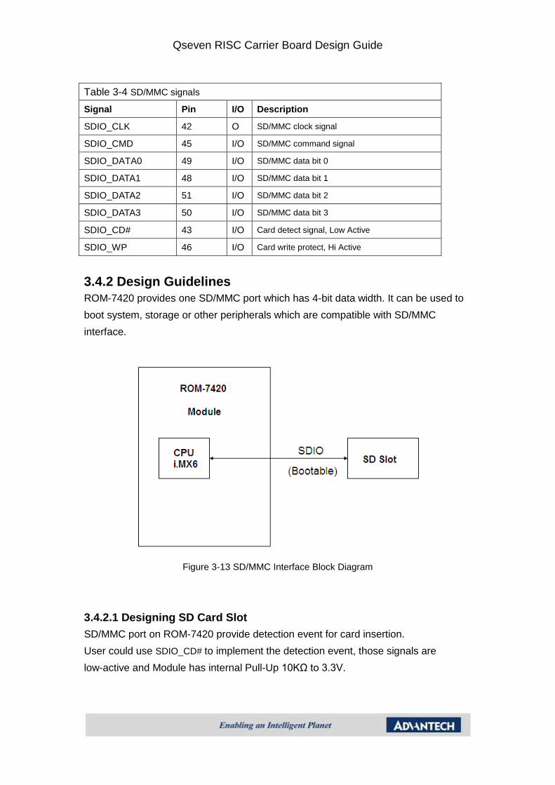
3.4.2 Design Guidelines
ROM-7420 provides one SD/MMC port which has 4-bit data width. It can be used to
boot system, storage or other peripherals which are compatible with SD/MMC
interface.
Figure 3-13 SD/MMC Interface Block Diagram
3.4.2.1 Designing SD Card Slot
SD/MMC port on ROM-7420 provide detection event for card insertion.
User could use SDIO_CD# to implement the detection event, those signals are
low-active and Module has internal Pull-Up 10KΩ to 3.3V.

Qseven RISC Carrier Board Design Guide
3.4.2.2 SD Slot Implementation
Figure 3-14 is an example of placing a SD card slot on carrier board. Q15 is a P
channel MOS-FET which supplies power to SD slot after SD card inserted into it. This
design is mainly to cut off supply power for card slot while SD card is not inserted into
slot.
User can choose an appropriate way to power the SD card. Please note that the
power supply sequencing of SD/MMC device must be considered if user requires the
booting from SD flash. The timing of supplying power must be provided in the same
time with SYS_3v3 supplied to module.
That's because the module will try to access SD device to boot after power-on reset
de-asserted; therefore, the SD device need be powered in time before de-asserting
power-on reset event on the module.
Figure 3-14 SD/MMC Reference Schematics
3.4.3 Layout Guidelines
Table 3-5 lists guidelines of SD/MMC signals in PCB routing stage, note that trace
width and spacing of single-ended signals differ from PCB stack and copper thickness;
even differ from each layer inside one PCB.
Table 3-5
Parameter Trace Routing
Maximum trace length allowance for all
signals on carrier board
5 inches
Single-ended impedance 50Ω ±10%
Length mismatch to clock
SD/MMC group
All trace length mismatch ≦ 200mil
Table 3.5 SD/MMC Trace Routing Guidelines

Qseven RISC Carrier Board Design Guide
3.5 LVDS Interface
3.5.1 Signal Description
Table 3-6 shows the ROM-7420 LVDS signals.
Table 3-6 LVDS signals
Signal Pin I/
O
Description
LVDS_A [0~3]+
LVDS_A [0~3]-
99, 101, 103,
105,107,109,
113,115
O LVDS Primary Channel differential pairs
LVDS_A_CLK+
LVDS_A_CLK-
119, 121 O LVDS Primary Channel differential clock
GP_I2C_DAT 125 I/
O
I2C data output for LVDS Primary Channel
display use
GP_I2C_CLK 127 I/
O
I2C clock output for LVDS Primary Channel
display use
LVDS_B [0~3]+
LVDS_B [0~3]-
100,102,104,
106,108,110,
114,116
O LVDS Secondary Channel differential pairs
LVDS_B_CLK+
LVDS_B_CLK-
120, 122 O LVDS Secondary Channel differential clock
LVDS_BLC_DAT 126 I/
O
I2C data output for LVDS Secondary Channel
display use
LVDS_BLC_CLK 128 I/
O
I2C clock output for LVDS Secondary
Channel display use
LVDS_PPEN 111 O LVDS panel power enable
LVDS_BLEN 112 O LVDS panel backlight enable
GP_PWM_OUT0 123 O LVDS panel backlight brightness control
3.5.2 Schematic Guidelines
The LVDS signals can be routed directly from the ROM-7420 module to the LVDS
connectors.Figure 3-15 shows one pair of LVDS connections. Each pair can use the
common-mode choke for EMI compliance if needed.
Figure 3-15 One LVDS Differential Pair with Choke Design

Qseven RISC Carrier Board Design Guide
3.5.3 Layout Requirements
The timing skew minimization requires trace length matching between chipset diepad
to the pins of the LVDS connector. Match the package length difference between
each signal group to minimize the timing variance. The ROM-7420 module has well
designed routing lengths to compensate for the mismatch length of the chipset
package.
Be sure to match the trace length on the carrier board. Table 3-7 shows the LVDS
Signals Trace Length Mismatch Mapping.
Table 3-7 LVDS Signals Trace Length Mismatch Mapping
Siganl group Data Pair Signal
matching
Clocks Associated
with the channel
Clock
Matching
Data To
Associated
Clock Matching
Matching
CHANNEL A
LVDS_A0+
LVDS_A0-
±5 mils
LVDS_A_CLK+
LVDS_A_CLK-
±5 mils
±100 mil
LVDS_A1+
LVDS_A1-
±5 mils
LVDS_A2+
LVDS_A2-
±5 mils
LVDS_A3+
LVDS_A3-
±5 mils
CHANNEL B
LVDS_B0+
LVDS_B0-
±5 mils
LVDS_B_CLK+
LVDS_B_CLK-
±5 mils
±100 mil
LVDS_B1+
LVDS_B1-
±5 mils
LVDS_B2+
LVDS_B2-
±5 mils
LVDS_B3+
LVDS_B3-
±5 mils
Each LVDS signal should be trace length matched to its associated clock strobe
within ±100 mils.
Routing for LVDS transmitter signals of different traces are terminated across 100 Ω ±
10% and should be routed as following points:
● It is necessary to maintain the differential impedance, Zdiff = 100 Ω ± 10%, where
all traces are closely routed in the same area on the same layer.

Qseven RISC Carrier Board Design Guide
● Isolate all other signals from the LVDS signals to prevent coupling from other
sources to the LVDS lines.
● The LVDS transmitter timing domain signals have maximum trace length of 6.8
inches. Please refer to Advantech layout checklist for detailed info.
● Clocks must be matched to the associated data signals to within ±100 mils.
● Minimum spacing between neighboring trace pair is 20 mils.
● Traces must be ground referenced.
● When choosing cables, it is important to remind that the differential impedance of
cable should be 95Ω. The cable length should be less than 0.5 meter for better signal
quality.
3.6 VGA
ROM-7420 Module provides analog display signals. There are three signals -- red,
green, and blue -- which send color information to a VGA monitor. Analog levels
between 0 (completely dark) and 0.7 V (maximum brightness) on these control lines
tell the monitor what intensities of these three primary colors to combine to make the
color of a dot (or pixel) on the monitor’s screen.
3.6.1 Signal Description
Table 3-8 shows ROM-7420 VGA signals
Table 3-8 VGA signals
Signal Pin I/O Description
VGA_RED 185 O Red analog video output signal for CRT monitors,
designed to drive a 75 Ω equivalent load.
VGA_GRN 187 O Green analog video output signal for CRT monitors,
designed to drive a 75 Ω equivalent load.
VGA_BLU 189 O Blue analog video output signal for CRT monitors,
designed to drive a 75 Ω equivalent load.
VGA_VSYNC 190 O Horizontal Sync: This output supplies the horizontal
synchronization pulse to the CRT monitor.
VGA_HSYNC 192 O Vertical Sync: This output supplies the vertical synchronization
pulse to the CRT monitor.
VGA_I2C_CK 186 O DDC clock line. It can be used for a DDC interface between the
graphics controller chip and the CRT monitor
VGA_I2C_DAT 188 I/O DDC data line. It can be used for a DDC interface between the
graphics controller chip and the CRT monitor
3.6.2 VGA Specifications
Please refer to “VESA and Industry Standards and Guidelines for Computer Display

Qseven RISC Carrier Board Design Guide
Monitor Timing Version 1.0, Revision 0.8” for the monitor timing specification.
3.6.3 Schematic Guidelines
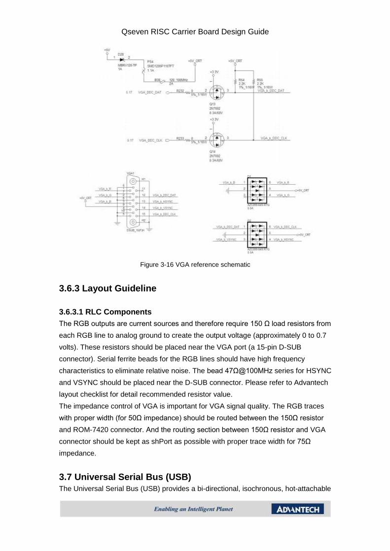
The reference schematic of VGA is shown in FIigure 3-16.
The VGA_I2C_CK and VGA_I2C_DAT signals must connect to the CRT monitor to
detect the plug-and-play and monitor-type info, the DDC pulled-up voltage is 3.3V on
module board , DO NOT pull up DDC signal on carrier board, you can through level
shift circuit to change pull up voltage from 3.3V to 5V. ESD protection voltage could
be 3.3V or 5V depends on the power map of the carrier board
Qseven RISC Carrier Board Design Guide
Figure 3-16 VGA reference schematic
3.6.3 Layout Guideline
3.6.3.1 RLC Components
The RGB outputs are current sources and therefore require 150 Ω load resistors from
each RGB line to analog ground to create the output voltage (approximately 0 to 0.7
volts). These resistors should be placed near the VGA port (a 15-pin D-SUB
connector). Serial ferrite beads for the RGB lines should have high frequency
characteristics to eliminate relative noise. The bead 47Ω@100MHz series for HSYNC
and VSYNC should be placed near the D-SUB connector. Please refer to Advantech
layout checklist for detail recommended resistor value.
The impedance control of VGA is important for VGA signal quality. The RGB traces
with proper width (for 50Ω impedance) should be routed between the 150Ω resistor
and ROM-7420 connector. And the routing section between 150Ω resistor and VGA
connector should be kept as shPort as possible with proper trace width for 75Ω
impedance.
3.7 Universal Serial Bus (USB)
The Universal Serial Bus (USB) provides a bi-directional, isochronous, hot-attachable

Qseven RISC Carrier Board Design Guide
Plug and Play serial interface for adding external peripheral devices such as game
controllers, communication devices and input devices on a single bus. ROM-7420
Modules provide one USB 2.0 port and one OTG port
3.7.1 Signal Description
Table 3-9 shows ROM-7420 USB signals, including pin number, signals, I/O and
descriptions.
Table 3-9 USB Signals Description
Signal Pin I/O Description
USB_P0-
USB_P0+
94, 96 I/O Universal Serial Bus Port 0 differential pair.
USB_P1-
USB_P1+
93, 95 I/O Universal Serial Bus Port 1 differential pair.
This port may be optionally used as USB client port.
USB_ID
92 I USB Host control select pin.
1: USB Port 1 as USB Client and enable USB Client
support
0: USB Port 1 as USB Host mode.
N/C if OTG port not used
USB_OTG_PEN 88 O Control the power source supplied to USB peripherals
500mA @5V in USB Host Mode. Active high.
USB_0_1_OC# 86 I Over current indicator from carrier board to Module
board. This pin is used to monitor the USB power
over current of the USB Ports 0 and 1.
USB_CC 91 I USB client present detect pin.
The USB OTG port may operate as USB client or
USB host.If USB OTG port is configured as client port
then this pin indicates that an external USB host is
connected to USB OTG port.
USB_VBUS 90 P USB VBUS pin. 5V tolerant. VBUS resistance has to
be placed on the module. VBUS capacitance has to
be placed on the carrier board
3.7.2 USB Spec.
Refer to “Universal Serial Bus Specification Revision 2.0, April 27, 2000”
3.7.3 Schematic Guidelines
Qseven RISC Carrier Board Design Guide
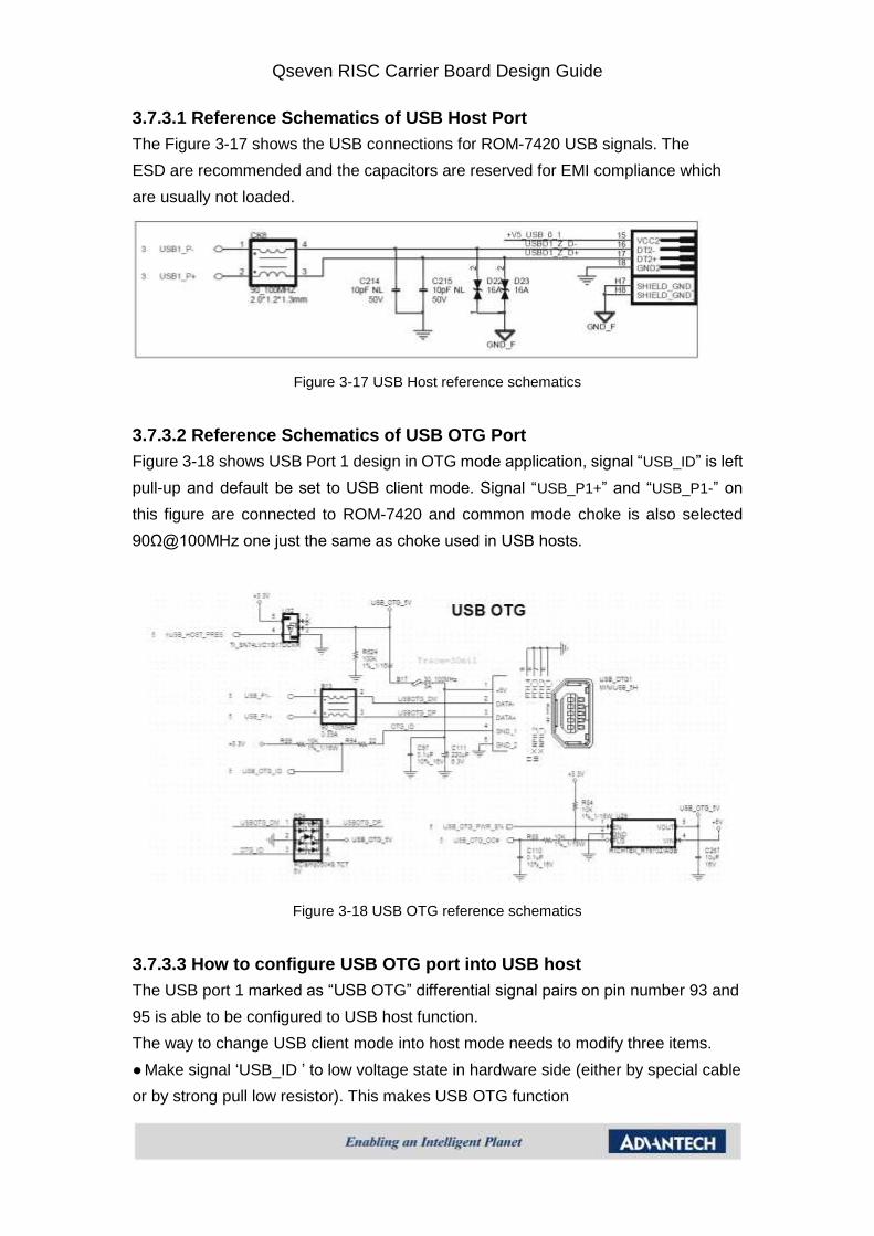
3.7.3.1 Reference Schematics of USB Host Port
The Figure 3-17 shows the USB connections for ROM-7420 USB signals. The
ESD are recommended and the capacitors are reserved for EMI compliance which
are usually not loaded.
Figure 3-17 USB Host reference schematics
3.7.3.2 Reference Schematics of USB OTG Port
Figure 3-18 shows USB Port 1 design in OTG mode application, signal “USB_ID” is left
pull-up and default be set to USB client mode. Signal “USB_P1+” and “USB_P1-” on
this figure are connected to ROM-7420 and common mode choke is also selected
90Ω@100MHz one just the same as choke used in USB hosts.
Figure 3-18 USB OTG reference schematics
3.7.3.3 How to configure USB OTG port into USB host
The USB port 1 marked as “USB OTG” differential signal pairs on pin number 93 and
95 is able to be configured to USB host function.
The way to change USB client mode into host mode needs to modify three items.
● Make signal ‘USB_ID ’ to low voltage state in hardware side (either by special cable
or by strong pull low resistor). This makes USB OTG function

Qseven RISC Carrier Board Design Guide
configured to host mode.
● Design power rail supplied to device, standard current is 500mA @ 5V per USB
port.
● Modify software program to become USB OTG compatible.
Note that the pin “USB_ID” is pull-up on ROM-7420 module, so this function would be
configured to client mode. If USB OTG port is not used on carrier board, it is
suggested to left this pin floating.
3.7.3.4 Low ESR Capacitor
The hot plug function is one of the popular features of the USB devices. The design
of the USB power-decoupling circuits must absorb the momentary current surge from
hot plugging an unpowered device. Reducing the capacity of decoupling capacitors is
not recommended. These USB power capacitors should be selected as low ESR and
low inductance.
3.7.3.5 ESD or EMI suppression components
Additional ESD or EMI suppression components could be implemented on the USB
data lines. It’s important to place the ESD and EMI components near the external
USB connector and make it grounded by the low-impedance ground plane.
The common mode choke is recommended to be used for USB2.0 EMI
consideration. Figure 3-19 shows the schematic of a typical common mode choke
and ESD suppression component, which are placed as close as possible to the USB
connector signal pins.
Figure 3-19 Common Mode Choke
The ESD components are generally needed for ESD testing. The common mode
chocks are generally adopted for USB 2.0 interface.
3.7.3.6 Over-Current Protection

Qseven RISC Carrier Board Design Guide
The Over-current protection on the external USB power lines is required to prevent
the power faults from external USB devices or cables. The USB_0_1_OC# signal is
used to input over-current conditions to the system hardware and software. The
over-current protection mechanism typically allows relatively high currents to flow for
small periods before the current goes over-limit or is interrupted
Figure 3-20 Overcurrent Circuit
The poly-switch in Figure 3-20 generally could not switch off fast enough. Overcurrent
caused by an external USB device may impact the power supply of the carrier board.
For fast response of sensing and power cutting, the active protection circuits shown in
Figure 3-21 are recommended. These devices may be used for per port protection of
the USB power lines and direct connected to the USB_0_1_OC# signal.
Figure 3-21 Power Switch with Overcurrent Protection Circuits
The over-current protection circuit is not implemented on the ROM-7420 Module.
It should be implemented on the carrier board.
3.7.4 Layout Guideline

Qseven RISC Carrier Board Design Guide
3.7.4.1 Differential pairs
The USB data pairs (ex. P0- and P0+) should be routed on the carrier board as
parallel differential pairs, with a differential impedance of 90 Ω. PCB layout software
usually allows determining the correct trace width and spacing to achieve this
impedance after the PCB stack-up configuration is known. As per usual differential
pair routing practices, the two traces of each USB pair should be matched in length
and kept at uniform spacing. Sharp corners should be avoided and be replaced by two
45° bends. Loop areas should be minimized and USB data pairs should be routed as
far from other signals as possible.
Figure 3-22 USB Layout Guidelines
3.7.4.2 Crossing a plane split
The mistake shown here is where the data lines cross a plane split. This causes
unpredictable return path currents and would likely cause a signal quality failure as
well as creating EMI problems.
Figure 3-23 Violation of Proper Routing Techniques

Qseven RISC Carrier Board Design Guide
3.8 Serial ATA
ROM-7420 Module provides up to four Serial ATA (SATA) interface, depending on
the chipset specs of the module.
3.8.1 Signal Description
Table 3-10 shows ROM-7420 SATA signals, including pin number, signals, I/O and
descriptions.
Table 3-10 SATA Signals Description
Signal Pin I/O Description
SATA0_TX+
SATA0_TX-
29,
31
O Serial ATA channel 0, Transmit Output differential pair.
SATA0_RX+
SATA0_RX-
35,
37
I Serial ATA channel 0, Receive Input differential pair.
3.8.2 Schematic Guidelines
3.8.2.1 Serial ATA AC Coupling Requirements
Both of TX and RX SATA differential pairs require AC coupling capacitors.All AC
coupling capacitorson the transmitter (TX) and receiver (RX) are placed on the
ROM-7420 Module. Do not place the AC coupling capacitors on the carrier board.
Figure 3-24 and Figure 3-25 show the connections.
Figure 3-24 SATA interconnection example

Qseven RISC Carrier Board Design Guide
Figure 3-25 SATA Schematic Reference
3.8.3 Layout Guidelines
3.8.3.1 General routing and placement
● Place the SATA connectors as closed as possible to the ROM-7420 Module.
The routing length total is recommended to be not more than 10 inches for SATA
Gen1 and 5 inches for SATA Gen2. The Intra-pair trace length distance matching
should be less than 5 mils.
● SATA signals must be ground referenced.
● Route all traces over continuous GND planes, with no interruptions. Avoid crossing
over anti-etched areas if at all possible. Any discontinuity or split in the ground plane
can cause signal reflections and should be avoid.
● Minimize layer changes. Use as few vias per SATA trace as possible (via count
should include through hole connectors as an effective via). If a layer change is
necessary, ensure that trace matching for either the TX or RX pair occurs within the
same layer.
● Do not route SATA traces under crystals, oscillators, clock synthesizers, magnetic
devices or ICs that use and/or duplicate clocks.
● Avoid stubs whenever possible. Utilize vias and connector pads as test points
instead.
● The SATA differential trace impendence target is 100 Ω ± 10%. Use an impedance
calculator to determine the trace width and spacing required for the specific board
stack-up being used, keeping in mind that the target is a 100 Ω ± 10%.
3.8.3.2 Serial ATA Trace length
● The length of the SATA differential pairs should be designed as short as possible.
For direct-connected topology where the SATA differential signal pair is routed
directly to a mobile SATA connector, It’s recommended the trace length total of SATA

Qseven RISC Carrier Board Design Guide
signals should be within 10 inches for SATA Gen1 and 5 inches for SATA Gen2 for
better signal integrity.
● The SATA differential pair traces should be length matched. The difference
between two line traces of TX / RX differential pairs should be restricted to less
than 5 mils, and less trace mismatch is recommended.
Figure 3-26 shows an example of SATA trace length pair matching. LA must equal to
LA‘, LB must equal to LB‘ , …and so on. It’s recommended to avoid the vias for layer
change, ensuring that the differential pairs are equal if necessary.
Figure 3-26 SATA traces length matching
3.9 PCI Express Bus
ROM-7420 provides a PCI Express Bus interface that is compliant with the PCI
Express Base Specification, Revision 2.0. It supports one general purpose PCI
Express port (x1).
3.9.1 Signal Description
Table 3-11 shows ROM-7420 PCI Express bus signals for general purpose.
Table 3-11 PCI-E Signals Description
Signal Pin I/O Description
PCIE0_TX+
PCIE0_TX-
179, 181 O PCI Express channel 0, Transmit Output
differential pair.
PCIE0_RX+
PCIE0_RX-
180, 182 I PCI Express channel 0, Receive Input differential
pair.
PCIE_CLK_REF+
PCIE_CLK_REF-
155, 157 O PCI Express reference clock output.
PCIE_WAKE# 156 I PCI Express Wake Event.
PCIE_RST# 158 O Reset signal for PCI Express device.

Qseven RISC Carrier Board Design Guide
PCIE_PWR_EN 172 O Turn on power for Express device.
PCIE_DIS# 178 O 3G/Wireless enable for external devices.
3.9.2 Schematic Guidelines
3.9.2.1 PCI Express AC Coupling Capacitor
Each PCI Express lane is AC coupled between its corresponding transmitter (TX)
and receiver (RX). Figure 3-27 and Figure 3-28 shows the connection for ROM-7420
signals and PCI Express connector. The AC coupling capacitors of TX+/- is present
on ROM-7420 Module. The AC coupling capacitors of RX+/- should be placed on the
carrier board and closely to the transmitter pins of the PCI Express devices.
Figure 3-27 PCI Express Interconnect Example

Qseven RISC Carrier Board Design Guide
Figure 3-28 PCI Express Connector Schematic Reference
Use the exact same package size for the capacitor on each signal in a differential pair.
Table 3-12 shows the PCI Express capacitor reference.
Table 3-12 PCI Express Capacitor Reference
Type Value Tolerance Placement
Length Matching
Between Differential
Pair
AC Capacitor 100nF 20% Recommended to place
close to the transmit side
As close as possible
between the differential
pairs
3.9.3 Layout Guidelines
This section shows the summary of the layout routing guidelines.
3.9.3.1 Differential pairs
The PCI Express signals should be routed as differential pairs. The following is a
summary of general routing guidelines for the differential pair traces.
In ROM-7420 platforms the PCI Express differential trace impendence target is 85 Ω ±
10%. It is important to equalize the total length of the traces in the pair throughout
the trace; each segment of trace length should be equal along the entire length of the
pair. Figure 2-30 shows an example. LA must equal to LA ‘ , LB must equal to LB‘ …,
and so on.
It is preferable to route TX and RX differential pairs alternately on the same layer at
outer layer and different layer at inner layer. Tight coupling within the differential pair
and increased spacing to other differential pairs helps to minimize EMI and crosstalk.
Qseven RISC Carrier Board Design Guide
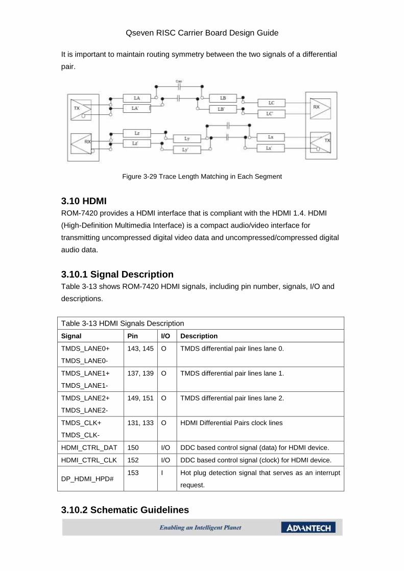
It is important to maintain routing symmetry between the two signals of a differential
pair.
Figure 3-29 Trace Length Matching in Each Segment
3.10 HDMI
ROM-7420 provides a HDMI interface that is compliant with the HDMI 1.4. HDMI
(High-Definition Multimedia Interface) is a compact audio/video interface for
transmitting uncompressed digital video data and uncompressed/compressed digital
audio data.
3.10.1 Signal Description
Table 3-13 shows ROM-7420 HDMI signals, including pin number, signals, I/O and
descriptions.
Table 3-13 HDMI Signals Description
Signal Pin I/O Description
TMDS_LANE0+
TMDS_LANE0-
143, 145 O TMDS differential pair lines lane 0.
TMDS_LANE1+
TMDS_LANE1-
137, 139 O TMDS differential pair lines lane 1.
TMDS_LANE2+
TMDS_LANE2-
149, 151 O TMDS differential pair lines lane 2.
TMDS_CLK+
TMDS_CLK-
131, 133 O HDMI Differential Pairs clock lines
HDMI_CTRL_DAT 150 I/O DDC based control signal (data) for HDMI device.
HDMI_CTRL_CLK 152 I/O DDC based control signal (clock) for HDMI device.
DP_HDMI_HPD# 153 I Hot plug detection signal that serves as an interrupt
request.
3.10.2 Schematic Guidelines

Qseven RISC Carrier Board Design Guide
3.10.2.1 EMI
The HDMI signals can be routed directly from the ROM-7420 module to the HDMI
connectors.Figure 3-30 shows one pair of HDMI connections. Differential pair can use
the common-mode choke for EMI compliance if needed.
Figure 3-30 One HDMI Differential Pair with common-mode Choke Design
3.10.2.2 DDC level shift
The HDMI_CTRL_DAT and HDMI_CTRL_CLK signals must connect to the HDMI
monitor to detect the monitor-type info, the DDC pulled-up voltage is 3.3V on module
board , DO NOT pull up DDC signal on carrier board, you can through level shift
circuit to change pull up voltage from 3.3V to 5V. ESD protection voltage could be
3.3V or 5V depends on the power map of the carrier board
Figure 3-31 HDMI DDC level-shift circuit Design
3.10.2.2 Reference schematic

Qseven RISC Carrier Board Design Guide
The reference schematic of HDMI is shown in FIigure 3-32. The HDMI_HPD must
have a buffer IC to change input voltage from 5V to 3.3V.
Figure 3-32 HDMI reference schematic
3.11 SPI Interface
Advantech ROM-7420 provides additional SPI interface for extended functions, for
example, user can attach a SPI flash device for storage purpose as well as ADC for
analog data acquirement, audio codec for audio applications, or I/O devices for
specific purposes such as a capacitive touch screen controller.
Please note that user CANNOT use this SPI interface for booting function.
3.11.1 Signal Description
Table 3-14 shows ROM-7420 SPI signals, including pin number, signals, I/O and

Qseven RISC Carrier Board Design Guide
descriptions.
Table 3-14 SPI Signals Description
Signal Pin I/O Description
SPI_MOSI 199 O Data out from module to carrie SPI
SPI_MISO 201 I Data in to module from carrier SPI
SPI_SCK 203 O Clock from module to carrier SPI
SPI_CS0 200 O Chip select for carrier board SPI – may be sourced from
chipset SPI0
SPI_CS1 202 O Chip select for carrier board SPI – may be sourced from
chipset SPI1
3.11.2 Schematic Guidelines
3.11.2.1 Reference schematic (Single Device)
SPI Point-to-Point Topology is shown in Figure 3-33.
Figure 3-33 SPI Point-to-Point Topology
3.11.2.2 Reference schematic (2 Flash Device)
Dual SPI Devices - Daisy Chain Topology is shown in Figure 3-34.

Qseven RISC Carrier Board Design Guide
Figure 3-34 SPI Daisy Chain Topology
3.11.3 Layout Guidelines
3.11.3.1 Layout guidelines for single device
Table 3-15 lists guidelines of SPI signals which is for single device in PCB routing
stage, note that trace width of single-ended signals differ from PCB stack and copper
thickness; even differ from each layer inside one PCB.
Table 3-15
Parameter Trace Routing
Maximum trace length allowance for all
signals on carrier board
8 inches
Single-ended impedance 50Ω ± 10%
3.11.3.2 Layout guidelines for dual device
Table 3-16 lists guidelines of SPI signals which is for dual device in PCB routing stage,
do not routing L2 or L3 trace length too long.

Qseven RISC Carrier Board Design Guide
Figure 3-35 Dual SPI ROM routing
Table 3-16
Parameter Trace Routing
L1 1.5 – 5.5”
L2 0.5 – 2.5”
L3 L2 ± 0.1”
Single-ended impedance 50Ω ± 10%
3.12 General Purpose Input/Output (GPIO)
ROM-7420 provides maximum 8 general purpose input / output signals to carrier
board. All signals operate at 3.3V level, those GPIO can not change its direction
dynamically.
3.13 CAN Bus
Controller Area Network (CAN or CAN-bus) is a message based protocol designed
specifically for automotive applications but now is also used in other areas such as
industrial automation and medical equipment.
ROM-7420 modules can optionally support two CAN bus ports.
3.13.1 Signal Description
Table 3-17 shows ROM-7420 CAN bus signals, including pin number, signals, I/O and
descriptions.
Table 3-17 CAN Signals Description
Signal Pin I/O Description
CAN0_TX 129 O CAN1 Transmit output
CAN0_RX 130 I CAN1 Receive input
CAN1_TX 144 O CAN2 Transmit output
CAN1_RX 146 I CAN2 Receive input

Qseven RISC Carrier Board Design Guide
3.13.2 Schematic Guidelines
it is necessary to add transceiver hardware on the carrier board. Please pay attention,
if use 5V transceiver, it must has a buffer IC to transfer voltage from 5V to 3.3V with
CAN0_RX signal, cause of CAN bus signal from CPU is 3.3V tolerance.
Figure 3-36 CAN bus reference schematic
3.14 I2C Bus Bus
Due to the simple two-wire serial bus protocol and the high availability of devices, the
I2C Bus is a frequently used low speed bus interface for connecting embedded
devices such as sensors, converters or data storage. ROM-7420 modules provide
one I2C bus on the module's connectors.
3.14.1 Signal Description
Table 3-18 shows ROM-7420 I2C bus signals, including pin number, signals, I/O and
descriptions.
Table 3-18 I2C Signals Description
Signal Pin I/O Description
I2C_CLK 66 I/O Clock line of I2C bus.
I2C_DAT 68 I/O Data line of I2C bus.
3.14.2 Design Guidelines
The maximum amount of capacitance allowed on I2C bus line (CLK, DAT) is 200pF
(determined by the 10KΩ pull-up resistor value on ROM-7420 module). A general
guideline of I2C standard mentioned that an IC input has 12pF capacitance and PCB
trace has 3.8pF capacitance per inch of trace length. Hence it is suggested that
customer place less than 12 devices for each I2C channel on carrier board. If device
number needs to be greater than 12, customer could add another 4.7KΩ pull-up
resistor on carrier board to give more driving strength and extend recommended
device number from 12 to 27.
Qseven RISC Carrier Board Design Guide
3.15 Watchdog control signals
The Watchdog on a ROM-7420 module can be hardware-triggered by an external
control circuitry. When generating a low level pulse on the ROM-7420 module's
'WDTRIG#' (Watchdog trigger signal) signal, the Watchdog timer will be reset and
restarted. If the Watchdog timer has expired without a software or hardware trigger
occurrence, the ROM-7420 module will do a internal reset by itself.
3.16 Power management signals
Table 3-19 Power Management Signals Description
Signal Pin I/O Description
PWGIN
26 I Power OK from main power supply. A high value
indicates that the power for module domain is good (Not
for carrier board circuits)
Pulled up on module.
CB_PWR_EN 18 O Carrier board circuits should not be powered up until the
module asserts the CB_PWR_EN signal.
RSTBTN#
28 I Reset input from carrier board. Carrier drives low to force
a Module reset.
Pulled up on module.
SLP_BTN# 21 I Sleep indicator from carrier board. May be sourced from
user Sleep button or carrier logic.
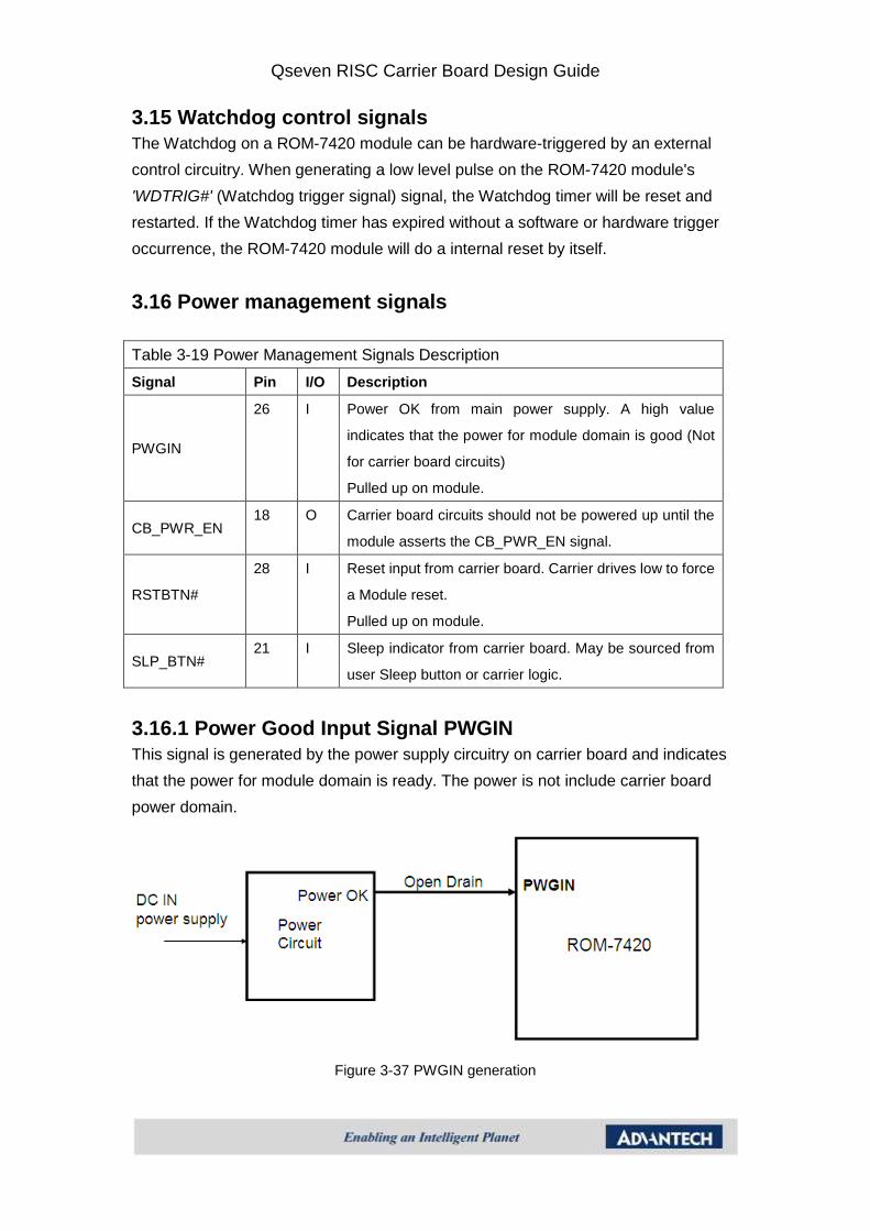
3.16.1 Power Good Input Signal PWGIN
This signal is generated by the power supply circuitry on carrier board and indicates
that the power for module domain is ready. The power is not include carrier board
power domain.
Figure 3-37 PWGIN generation
Qseven RISC Carrier Board Design Guide
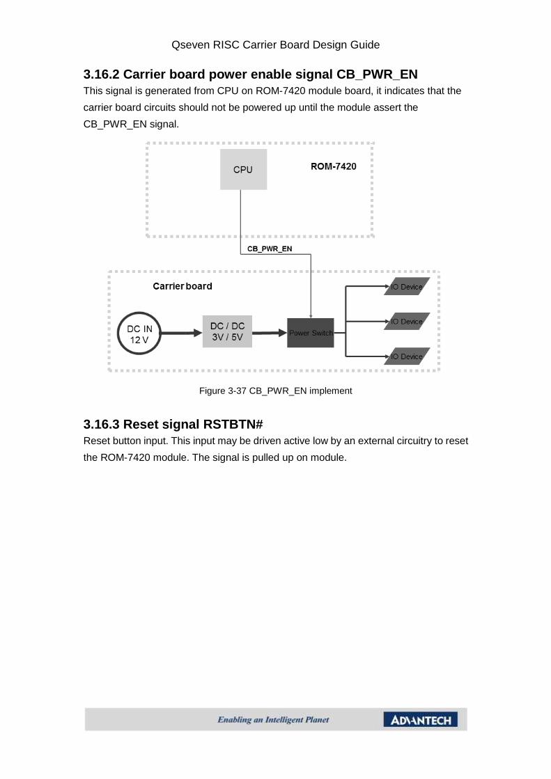
3.16.2 Carrier board power enable signal CB_PWR_EN
This signal is generated from CPU on ROM-7420 module board, it indicates that the
carrier board circuits should not be powered up until the module assert the
CB_PWR_EN signal.
Figure 3-37 CB_PWR_EN implement
3.16.3 Reset signal RSTBTN#
Reset button input. This input may be driven active low by an external circuitry to reset
the ROM-7420 module. The signal is pulled up on module.

Qseven RISC Carrier Board Design Guide
Chapter 4 Input Power
This chapter provides the power supply design recommendations for ROM-7420 and
provide customer’s carrier board design reference.
4.1 Module power supply range
Table 4-1 Power supply range
Power Supply Minimun Nominal Maximum
VCC 4.75V 5.00V 5.25V
4.2 Module power DC Characteristics
Table 4-2 Power consumption
Power
Supply
Voltage (V) Standby Mode
(A)
Typical (A) Maximum (A)
VCC 5.00V N/A N/A 0.6306
4.3 Power Delivery Block Diagram
Figure 4-1 Carrier Board Reference Power Delivery Block Diagram
4.3 System Power Domains
It is useful to describe an system as being divided into a hierarchy of two power
domains:
(1) ROM-7420 Module power domain
(2) Carrier Board Circuits power domain
The ROM-7420 Module domain includes the ROM-7420 module and may include a
serial EEPROM on the carrier board, connected to the I2C_PM I2C bus in the Module

Qseven RISC Carrier Board Design Guide
power domain, allowing Module software to read carrier board parameters. The
carrier circuits domain includes “every thing else” (and does not include items from
the Module domain, even though they may be mounted on the carrier).
Figure 4-2 System power domain
4.4 RTC Battery Implementation
If customer needs to keep timer while system power off, a coin battery is required.
Figure 4-3 gives an example of designing coin battery circuits. Using battery is
Rayovac® BR2032 non-rechargeable coin battery, with battery capacity 195mAh and
working temperature -40~85℃. R199 in this figure is an easy current limit circuit to
protect over discharge situation.
Figure 4-3 RTC Coin Battery Circuits
Qseven RISC Carrier Board Design Guide
Chapter 5 PCB Layout Guidelines
A brief description of the Printed Circuit Board (PCB) for ROM-7420 based boards
is provided in this section. From a cost- effectiveness point of view, the four-layer
board is the target platform for the motherboard design. For better quality, the
six-layer or eight-layer board is preferred.
5.1 Nominal Board Stack-Up
The trace impedance typically noted (50 Ω ± 10%) is the “nominal” trace impedance
for a 5-mil wide external trace and a 4-mil wide internal trace. However, some
stackups
may lead to narrower or wider traces on internal or external layers in order to meet the
50 Ω ± 10% impedance target, that is, the impedance of the trace when not subjected
to the fields created by changing current in neighboring traces. Note the trace
impedance target assumes that the trace is not subjected to the EMI fields created by
changing current in neighboring traces.
It is important to consider the minimum and maximum impedance of a trace based on
the switching of neighboring traces when calculating flight times. Using wider spaces
between the traces can minimize this trace-to-trace coupling. In addition, these wider
spaces reduce settling time.
Coupling between two traces is a function of the coupled length, the distance
separating the traces, the signal edge rate, and the degree of mutual capacitance
and inductance. Also, all high speed signals should have continuous GND referenced
planes and cannot be routed over or under plane splits.
Qseven RISC Carrier Board Design Guide
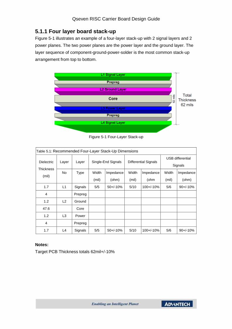
5.1.1 Four layer board stack-up
Figure 5-1 illustrates an example of a four-layer stack-up with 2 signal layers and 2
power planes. The two power planes are the power layer and the ground layer. The
layer sequence of component-ground-power-solder is the most common stack-up
arrangement from top to bottom.
Figure 5-1 Four-Layer Stack-up
Table 5.1: Recommended Four-Layer Stack-Up Dimensions
Dielectric
Thickness
(mil)
Layer Layer Single-End Signals Differential Signals USB differential
Signals
No Type Width
(mil)
Impedance
(ohm)
Width
(mil)
Impedance
(ohm
Width
(mil)
Impedance
(ohm)
1.7 L1 Signals 5/5 50+/-10% 5/10 100+/-10% 5/6 90+/-10%
4 Prepreg
1.2 L2 Ground
47.6 Core
1.2 L3 Power
4 Prepreg
1.7 L4 Signals 5/5 50+/-10% 5/10 100+/-10% 5/6 90+/-10%
Notes:
Target PCB Thickness totals 62mil+/-10%

Qseven RISC Carrier Board Design Guide
5.1.2 Six layer board stack-up
Figure 5-2 illustrates an example of a six-layer stack-up with 4 signal layers and 2
power planes. The two power planes are the power layer and the ground layer. The
layer sequence of component-ground-IN1-IN2-power-solder is the most common
stack-up arrangement from top to bottom.
Figure 5-2 Six-Layer Stack-up
Table 5.2: Recommended Six-Layer Stack-Up Dimensions
Dielectric
Thickness
(mil)
Layer Layer Single-End Signals Differential Signals USB differential
Signals
No Type Width
(mil)
Impedance
(ohm)
Width
(mil)
Impedance
(ohm
Width
(mil)
Impedance
(ohm)
1.7 L1 Signals 5/5 50+/-10% 5/10 100+/-10% 5/6 90+/-10%
4 Prepreg
1.2 L2 Ground
4 Core
1.2 L3 IN1 5/5 50+/-10% 5/10 100+/-10% 5/6 90+/-10%
38 Prepreg
1.2 L4 IN2 5/5 50+/-10% 5/10 100+/-10% 5/6 90+/-10%
4 Core
1.2 L5 Power
4 Prepreg
1.7 L6 Signals 5/5 50+/-10% 5/10 100+/-10% 5/6 90+/-10%
Qseven RISC Carrier Board Design Guide
Notes:
Target PCB Thickness totals 62mil+/-10%
Qseven RISC Carrier Board Design Guide
5.2 Alternate Stack Ups
While the different stack-ups are needed (number of layers, thickness, trace width,
etc.), the following key points should be noted:
1. Final post lamination, post etching, and post plating dimensions should be used for
electrical model extractions.
2. All high-speed signals should reference solid ground planes through the length of
their routing and should not cross plane splits. To guarantee this, both planes
surrounding strip-lines should be GND.
3. High-speed signal routing should be done on internal strip-line layers. High-speed
routing on external layers should be minimized to avoid EMI. Routing on external
layers also introduces different delays compared to internal layers. This makes it
extremely difficult to do length matching if routing is done on both internal and external
layers.
4. Two layer board stack-up has poor EMI shielding and ESD protection
characteristics, so it is not recommended to be designed in.
5.3 Differential Impedance Targets for Trace Routing
Table 5.3 shows the target impedance of the differential signals. The carrier board
should follow the required impedance in this table.
Table 5.3 Differential Signals Impedance Requirement
Signal Type Impedance
HDMI 100 Ω ± 10%
LVDS 100 Ω ± 10%
SATA 100 Ω ± 10%
USB 90 Ω ± 10%
PCI Express 85 Ω ± 10%
LAN 100 Ω ± 10%

Qseven RISC Carrier Board Design Guide
Chapter 6 Mechanical Characteristics Guidelines
6.1 ROM-7420 Mechanical Dimensions
The PCB size of the ROM-7420 module is 70mm x 70mm. The PCB thickness is
1.2mm to allow high layer count stack-ups. Figure 6-1 shows the ROM-7420 module
board mechanical dimensions, unit is millimeter. The 230 pin connector pair shall be
mounted on the backside of the PCB and is seen “through” the board in this view.
The holes shown in this drawing are intended for mounting the module / heatspreader
combination to the carrier Board. An independent, implementation specific set of
holes and spacers shall be used to attach the heat-spreader to the module. Figure 6-1
shows the ROM-7420 Module board mechanical dimensions. The unit is millimeters.
Figure 6-1 ROM-7420 Module Board Mechanical Dimensions
6.2 Carrier Board Connector
The carrier board utilizes a 230-pin card-edge connector to connect the ROM-7420
module. Originally, this card-edge connector was designed for MXM graphics
modules that are used for PCI Express capable notebook graphics cards. The
card-edge connector is following the MXM specification and therefore this connector
type is also known as a MXM connector.
The MXM edge connector is the result of an extensive collaborative design effort with
the industry's leading notebook manufacturers. This collaboration has produced a

Qseven RISC Carrier Board Design Guide
robust, low-cost edge connector that is capable of handling high-speed serialized
signals.
The MXM connector accommodates various connector heights for different carrier
board applications needs. This specification suggests two connector heights, 7.8mm
and 5.5mm.
6.2.1 MXM Connector Dimensions
Figure 6-2 MXM Connector
Qseven RISC Carrier Board Design Guide
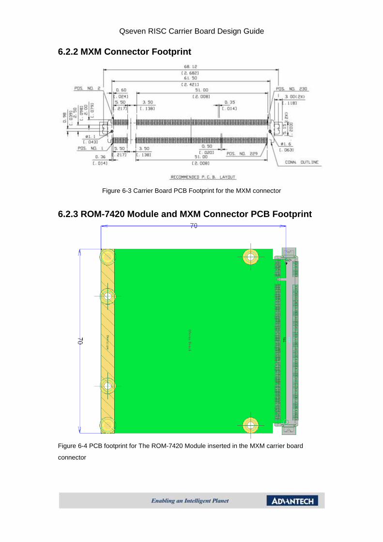
6.2.2 MXM Connector Footprint
Figure 6-3 Carrier Board PCB Footprint for the MXM connector
6.2.3 ROM-7420 Module and MXM Connector PCB Footprint
Figure 6-4 PCB footprint for The ROM-7420 Module inserted in the MXM carrier board
connector