roll-to-roll processing for solution processed oled … processing for solution processed oled ......
TRANSCRIPT

Roll-to-Roll Processing for Solution Processed OLED Devices
Joanne Wilson, Pit Teunissen, Ton van Mol, Juliane Tripathi, Hylke Akkerman, Sandeep Unnikrishnan, Ike de Vries, Eric Rubingh, Robert Abbel, Pim Groen

© Holst Centre
Vision on lighting
© Holst Centre
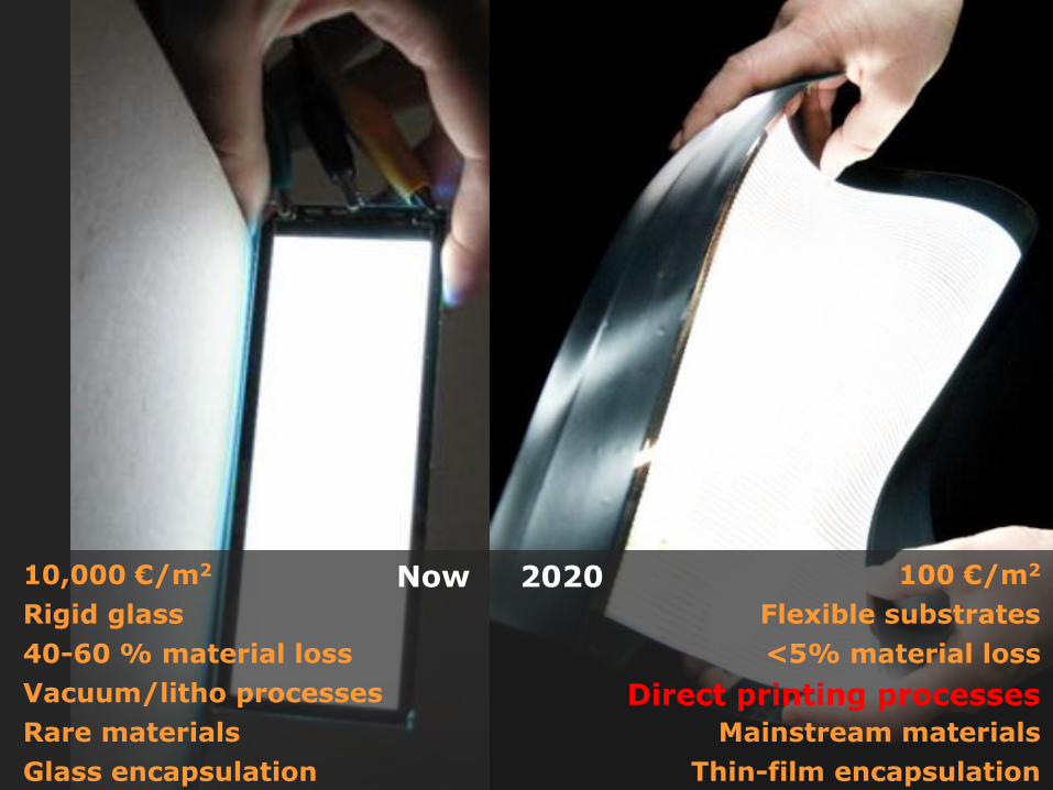
10,000 €/m2
Rigid glass
Vacuum/litho processes
40-60 % material loss
Glass encapsulation
Rare materials
100 €/m2
Flexible substrates
Direct printing processes
<5% material loss
Thin-film encapsulation
Mainstream materials
2020 Now

© Holst Centre
R2R Printing & Coating technology
< 4 OLED Processing
< 4
Why?
Printing/casting preferred over lithographic patterning
• easier for large scale processing
• fine features/patterning without complicated masks
• higher materials utilisation lower cost
Topics:
S2S up scalable to R2R
Multilayer coating
Patterning & alignment
Prevention of contamination – yield control

© Holst Centre
Summary: Schematic of R2R solution processed OLED (ITO free)
< 5
1. Printing and sintering of silver grids (anode)
3. Shunting cathode OLEDs by IJP
2. Large area coating
4. R2R Barrier

© Holst Centre
1. Printing & Sintering
• Printing silver: Ink jet – Screen printing
• Baseline Process: Thermal Sintering in furnace at high
temperatures (30 min./>150 oC )
Limited to Tg of polymer foils
Slow and inefficient process
In R2R line with 6 m/min a furnace of 60 m needed
• Photonic Flash Sintering
< 6

© Holst Centre
Photonic sintering principle
1,00E+00
1,00E+01
1,00E+02
1,00E+03
1,00E+04
1,00E+05
1,00E+06
1,00E+07
1,00E+08
0 10 20 30 40 50
Time (s)
Res
ista
nce
(O
hm
)
< 7
Light source
The principle of photonic sintering is the selective heating of the ink
Lamps are chosen such that the light is mainly absorbed in the printed structures, not substrate
200 300 400 500 600
0,0
0,5
1,0
No
rmalis
ed a
bso
rption
(nm)
Conductive Ink
Plastic Foil
Lamp spectrum
Achievements:
- Sintering time reduced from minutes to few seconds!
Optimized Flash sintering
Oven sintering (130°C)
Result feasibility study photonic sintering of Ag-based inks

© Holst Centre < 8
Extended to 5 print heads

© Holst Centre < 9
Holst Centre’s Approaches: 0) Spin coating: simple, no patterning
1) Ink-jet printing: non-contact, patterning is easy - Homogeneity over large areas needs to be investigated
2) Slot-die coating: non-contact, large area blanket coating
- Pattering: via laser ablation or selective wetting/dewetting or
stripe coating and intermittant coating
2. Large area coating (using solution processing)

© Holst Centre < 10
Slot die casting at Holst
-Pattering !!! -R2R atmosphere control -Yield

© Holst Centre
Integration at Holst Centre
< 11

© Holst Centre < 12
© Holst Centre < 13
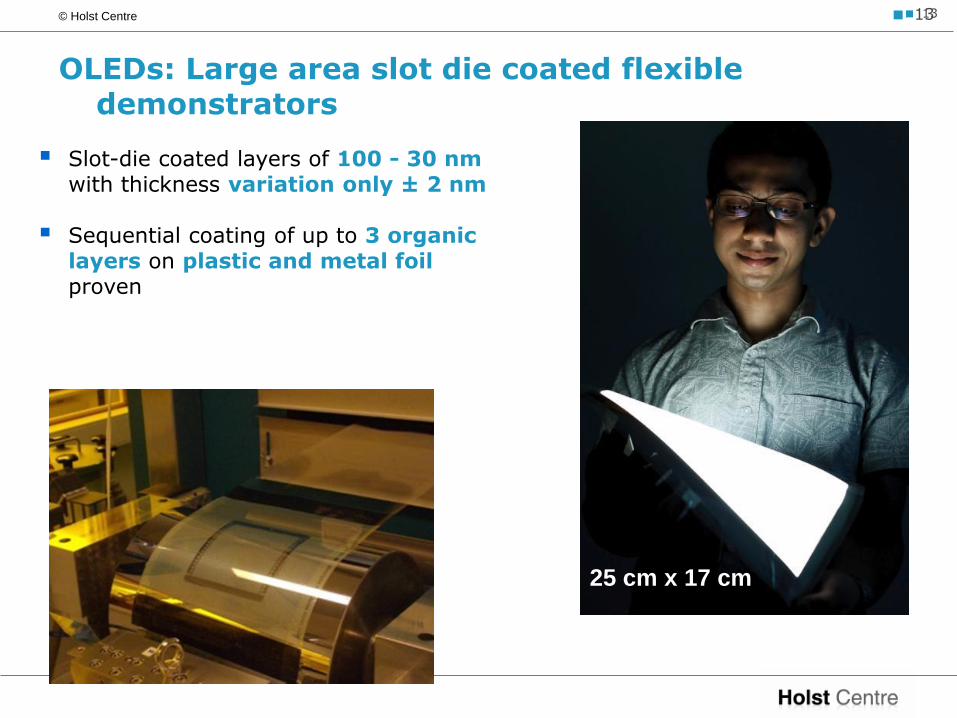
OLEDs: Large area slot die coated flexible demonstrators
25 cm x 17 cm
Slot-die coated layers of 100 - 30 nm with thickness variation only ± 2 nm
Sequential coating of up to 3 organic
layers on plastic and metal foil proven
< 13

© Holst Centre
Roll-to-roll multilayer coating of OLEDs
< 14

© Holst Centre
Roll-to-roll multilayer solution coated OLEDs on flexible metal foil
8 cm x 8 cm devices with performance not far from smaller sheet-to-sheet processed OLEDs
< 15
Homogeneity 60% @ 1000 cd/m2 mostly limited by transparent electrode conductivity

© Holst Centre
Holst Centre multicoat (2 x slot coating) pilot production line
• Unique concept where web is never touched on topside essential for Oled production.
• Concept makes very efficient use of cleanroom space.
• Slot die coating in controlled atmosphere (all coating and
drying in Nitrogen environment if needed).
• Closed furnace (class 10 + < 10 ppm O2/H2O)
< 16
Class 1000
Class 10 <10 ppm O2
Local Class 100

© Holst Centre
Multicoat R2R line
< 17

© Holst Centre
Summary: Schematic of R2R solution processed OLED (ITO free)
< 18
1. Printing and sintering of silver grids (anode)
3. Shunting cathode OLEDs by IJP
2. Large area coating
4. R2R Barrier

© Holst Centre < 19
Without shunting lines: Inhomogeneous due to limited conductivity of transparent cathode
Device size 80 x 80 mm2
3. IJP grid to improve transparent electrode conductivity

© Holst Centre < 20
With ink jet printed shunting lines: Less inhomogeneous due to shunt lines

© Holst Centre
4. Barrier Requirements Organic Electronics
< 21

© Holst Centre
S2S Thin Film Barrier Technology @ Holst Centre
• Holst Centre barrier fundamentals:
Multilayer thin film barrier
PECVD SiN – organic coating – PECVD SiN
Inorganic layer (PECVD SiN)
real barrier with WVTR < 10-6 g/m2/day
full coverage of cathode
Organic layer
decouple pinholes
Only 3 layers to keep costs low
Transparent:
suitable for top-emission or bottom-emission OLEDs
< 22
• Validation done on real OLEDs against product spec:
Black spot analysis in accelerated shelf lifetime test (60oC/90% RH)
Organic coating 2
SiN
Organic coating 1
25-200 μm Polymer foil
Organic coating 3
Organic coating 4
Device

© Holst Centre
4 R2R barrier film
< 23
• WVTR of the single SiN sampled over 350m length at 60oC and 90%RH for 20 days : Overall WVTR = (5±1)·10-5 g/m2day
• 450 m/day
• Full barrier stack R2R processed (OCP-SiN-OCP-SiN)
© Holst Centre < 24
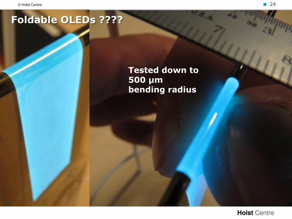
Tested down to 500 µm bending radius
Foldable OLEDs ????

Novel Aerospace Materials 25|30
Integration
Smart placemat to improve people’s diet
Wristband for reminders and feedback
Force-sensitive grip for expressing anxiety
Intuitive interface for Emergency defibrilator
+ =
Light Touch Matters

© Holst Centre
Conclusion Lighting based on printing/ coating technologies
The research leading to these results has received funding from the European Union Seventh Framework Programme (FP7/2007-2013) under grant agreement no 281027 and 310311
< 26