roll-to-roll manufacturing of advanced touch panel … · roll-to-roll manufacturing of advanced...
TRANSCRIPT

External Use
External Use
Roll-to-Roll Manufacturing of Advanced Touch Panel Devices
Neil Morrison Manager R&D, R2R PVD/CVD, Web Coating Group, AEP, Applied Materials
Aimcal Europe, Prague, Czech Republic Date: 11th June, 2012

External Use
2
Outline
Applied Materials & The Mobility Age
Touch Panel Production Equipment
Current 150 Ω/□ Invisible ITO Performance
Towards 100 Ω/□ Invisible ITO for Film Based Devices
Influence of Scaling & Cathode Type on Productivity & CoO
Summary

External Use
Solar
The Most Exciting Industries on Earth
3
20,000,000x reduction in
COST PER TRANSISTOR in 30 years1
20x reduction in
COST PER AREA in 15 years2
5x reduction in
COST PER WATT in 4 years3
At 1976 transistor prices, an iPod® would have cost $3.2B
1 Source: SIA, IC Knowledge LLC 2 Source: Display Search, Nikkei BP, Applied Materials
3 Source: Photon Consulting 2012
Display Semiconductor

External Use
Mega Trends
The Mobility Age
Clean Energy

External Use
Performance at Low Power New Architectures More Transistors
Enabling Mobility Age
5
Mobile End Markets
3D Transistors
Moore’s Law Scaling

External Use
Large Screen TV
Laptop PC
Mobility Creating “Fourth Wave” in Displays
Smart Phones and Tablets
Desktop Monitor
6
External Use
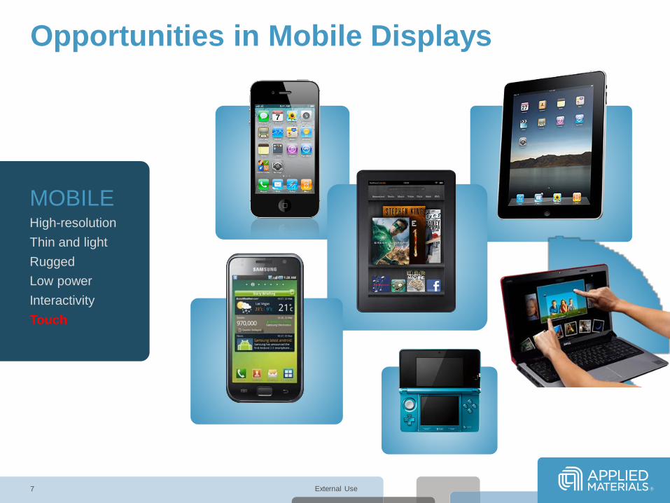
Opportunities in Mobile Displays
7
MOBILE High-resolution Thin and light Rugged Low power Interactivity Touch

External Use
Applied Materials Display Product Landscape
8
NEW EQUIPMENT SEGMENTS CORE TFT-LCD EQUIPMENT
Major End Products
Equipment Applications
Products
TV Monitor & Notebook
+LTPS + Metal oxide + Touch
OLED TV Tablet Smart Phone ADAPTING
LTPS Executing
Touch Executing
Metal Oxide
Developing
Expanding portfolio to grow in new segments
CVD Array
PVD Array
Array Test
PVD Color Filter

External Use
Mobile Application Demand Driving New Technologies
9
0
2
4
6
8
10
12
14
16
2010 2012F 2015F
Area
Dem
and(
M m
2)
SmartPhone and Tablet Demand
Units(M) 2010 2012 2015 CAGR*
Smartphone 297 685 1,254 33%
Tablets 18 109 225 67% Tablet
70%
CAGR* (area)
OLED SmartPhone (LTPS)
High-res SmartPhone (LTPS)
Low resolution Smartphone (a-Si)
Low-Res Tablet (a-Si)
High-res Tablet (MO)
OLED Tablet (LTPS)
Sm
artPhone
44%
* CAGR 2010-2015
Source : DisplaySearch, Applied Materials

External Use
Applied Inside Tablet PC
10
Display Enabled by Applied Materials’
PE-CVD, PVD, Test, and Roll-to-Roll Equipment
(>30% of tablet BOM*)
Semiconductor Enabled by Applied Materials’
Silicon Systems Equipment - Microprocessor
256MB DRAM 16GB MLC NAND Flash
I/O Controller Multi-Touch Controller (>20% of tablet BOM*)
Source: iFixit, UBS, Applied Materials * Refers to % of Bill of Materials processed by Applied Materials equipment

External Use
SmartWeb™ Product
SmartWeb SL
SmartWeb XL
11
System for Lab and Pilot production Web Width: 400 – 600 – 800mm 3 Cathodes Per Drum 1 or 2 Drum System
System for Mass Production Web Width: 1000 – 1400mm 6 Cathodes Per Drum 1 or 2 Drum System

External Use
Primary Process Module (up to 6 cathodes around
temp controlled drum)
Unwinder Module
Rewinder Module
Interleaf Take-Up Option
Interleaf Pay-Out Option
Load Locks
Separately pumped process zones for
excellent gas separation Option
Expansion Module Option
(thermal process or backside cathodes)
Standardized interfaces for wide variety of cathode choices
SmartWeb™ Modular Platform Architecture

External Use
Inline Process Monitoring & Control
13
R
Photometry
T
Inline Process Monitoring & Control Necessary for Yield
Enhancement in R2R!
Measuring Roller(- Potential)
R F I F
U F
Measurement Roller
Measurement Roller

External Use
14
Wide Variety of High Performance Sources
14
TwinMag™ Planar AC Cathodes for Dielectrics
TwinMag Rotatable AC Cathodes for Dielectrics.
High Utilization DC Planar Cathodes
Super-High Utilization DC Rotatable Cathodes
Delivering Flexible Process Capability
In-situ Pre-Clean/Pre-Treatment Sources

External Use
Rotary Cathode Technology for TP Continuous Target Rotation Ensures Clean Target Surface
– Minimized Particle Buildup and Emission • Dramatically Reduced ITO Nodule Density
– Maximized Process Stability and Target Utilization (> 80 %)
15

External Use
16
Improving CoO & Performance Si
Reduces Material Costs, Particles & Maintenance!
NbOx Cost Down ITO MoNb AlNd

External Use
SmartWeb Highlights Field Proven Technology
– Highest Install Base in Industry – Industry Leading Platform Serving Digital Resistive & Projective Capacitive
Markets – Sputter up Configuration to Eliminate Particulate Incorporation
Best in Class Substrate Handling – Minimized Number of Guide Rollers in Contact with the Coated Surface – Perfect Roller Parallelism
Superior Cathode Technology – Demonstrated Process Stability – Best in Class Gas Separation – Best in Class Productivity – Multi Process Flexibility – Closed Loop Control
17

External Use
Invisible ITO (For Projective Capacitive Touch)
18
PET
(HardCoat)
SiO2
ITO
RITO REtch
RITO REtch
PET
(HardCoat) SiOx
ITO
X-Layer
Y-Layer
4-layer system
RITO REtch
RITO REtch
Optical Matching Required for Patterned ITO Electrodes
Good Index Matching (Invisibility) Possible for Thin ITO Layers

External Use
Benchmark Invisible-ITOTM on R2R HC-PET
19
Rs (Ohm/Sqr)
Ty ITO (%)
b*
Ty no ITO (%)
b*
Ry ITO (%)
Ry no ITO (%)
Delta R / % (420-700nm)
270 89.5 0.6 89.4 0.8 9.6 9.4 < 0.7
200 88.7 0.85 89 0.9 11.4 10.7 < 1.3
150 89.9 0.8 90.0 0.3 9.3 9.6 < 1.8
Polymer (e.g. HC PET)
Invisibility Layers TCO (e.g. ITO)
150 Ω/□ Required for 5-10” PCT Devices-Trend Moving to 100 Ω/□ for > 10”
External Use
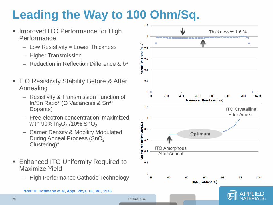
Leading the Way to 100 Ohm/Sq. Improved ITO Performance for High
Performance – Low Resistivity = Lower Thickness – Higher Transmission – Reduction in Reflection Difference & b*
ITO Resistivity Stability Before & After
Annealing – Resistivity & Transmission Function of
In/Sn Ratio* (O Vacancies & Sn4+
Dopants) – Free electron concentration* maximized
with 90% In2O3 /10% SnO2
– Carrier Density & Mobility Modulated During Anneal Process (SnO2 Clustering)*
Enhanced ITO Uniformity Required to Maximize Yield
– High Performance Cathode Technology
20
Thickness± 1.6 %
Optimum
ITO Amorphous After Anneal
ITO Crystalline After Anneal
*Ref: H. Hoffmann et al, Appl. Phys, 16, 381, 1978.

External Use
Process Optimization for 100 Ohm/Sq. Metallic Working Points Provide Route to Lower Resistivity Material
21
Interstitial/GB Oxygen Incorporation
Stochiometric Incorporation
*Ref: H. Hoffmann et al, Appl. Phys, 16, 381, 1978.

External Use
Influence of Annealing/Lamination Anneal Process Typically Performed During Lamination Step Annealing Increases Charge Carrier Density & Hall Mobility*
– Oxygen Vacancies Created by Desorption of Oxygen from Bulk Film→ ρ & Rs ↓ – Interstitial/GB Oxygen Removed (Reduction in Density of Electron Traps) – Bulk Defect Density Reduction/Removal of Lattice Defects → Ty & σ ↑ ρ & Rs ↓
22
*Ref: H. Hoffmann et al, Appl. Phys, 16, 381, 1978.

External Use
Significant Savings in Simple ITO Calculation Example:- R2R Invisible ITO Layer Stack 200 Ω/□
23
Cost Down
Remark: Target Prices Depend Strongly on Yearly Consumption

External Use
Productivity & Cost Optimization
24
Impact of Scaling & Cathode Technology – Calculation Example:- R2R Invisible ITO Layer Stack 200 Ω/□
Expected Productivity Improvement by Scaling
– 2 Drum vs 1 Drum – Significant Gain with Use of DC Rotatable Cathode Technology
Cost/Area Cannot be Driven Down by Scaling Only – CoO Limited by ITO Cost – DC Target Utilization Dramatically Improved Using Rotatable Technology

External Use
Reinforcing a Touch-Panel World AMAT Offers Production Solutions for Foil Based Touch
Panel Sensor Architectures
Key Focus to Increase Scale and Reduce Cost
Superior Cathode and Inline Metrology Technology Available to Maximize Yield
150 Ω/□ at 90 % Transmission Current Standard for 7-10“ Tablet Displays → Trend Moving to 100 Ω/□ for > 10 “
Solutions Available to Increase Product Value for Both User and Touch Panel Manufacturer
Prepared for Next Generation Touch Devices, Today

External Use
Reinforcing Touch-Panel World!
ありがとう 감사합니다
謝謝 Thank You
Danke Schön


External Use
Choosing Substrate & Value Proposition
28
Flexibility
Glass Rigid plastic Film
Lower CapEx
Thickness/Weight Reduction
Optical Performance
Film Conductivity
Hardness, Durability
AKT Aristo TWINTM SmartWebTM
Dynamic Deposition Glass and Rigid
Substrates
Roll-to-Roll Deposition Polymer Film &
Flexible Substrates
Scratch Resistant Large Area Narrow Bezel
Shatterproof Lightweight
Quick to Market
Key Manufacturing Requirements: Process Freedom, Configuration Flexibility, Optimum Layer Properties

External Use
Dramatic Response to Growth
Recent R2R/Display Milestones: Released Higher Rate Planar Cathode Technology (Productivity & CoO) Qualified Multiple Target Suppliers Inclusive Rotary ITO (Productivity & CoO) Released Improved SiO2 Process Closed Loop Control (Yield) Improved R2R ITO Resistivity to Meet 150 Ω/□ Demand (End Product Value) Invisible ITO BKM for Film Based Tablet Devices (End Product Value)
Glass R2R
29

External Use
New Aristo Highlights Field Proven Technology
– More Than 40 Systems for PCT Installed Rotary Target PVD Technology
– Process Stability Even with Reactive Processes – Superior Particle Performance – Extended Uptime Due to High Target Utilization – Lowest ITO Resistivity – High Productivity – Superior Yield
30

External Use
31
Delivering Manufacturing Scale Driving Lower Costs
AT 1976 TRANSISTOR PRICES AN iPOD® WOULD HAVE COST $3.2B
FIRST
Cost Per Transistor 20,000,000x
cost reduction over 30 years1
THEN
Cost Per Area 20x
cost reduction over 15 years2
NOW
Cost Per Watt Toward grid parity
1 Source: SIA, IC Knowledge LLC 2 Source: Display Search, Nikkei BP, Applied Materials

External Use
USER GUIDE: Corporate Overview REMOVE PRIOR TO PRESENTATION
Feedback and contact: [email protected]
32
This is Applied Materials official corporate overview last updated as of
February 16, 2012.
This presentation is targeted to potential new customers or suppliers, new hires and recruiting, government officials, and other business contacts and provides
an introduction and high level overview of Applied Materials.
Speak with energy, authority and ensure that you connect with the audience.
Make your presentation highly interactive.
Engage with your audience before you start your presentation and keep checking in that they are getting the information they need from you and from
Applied Materials.
Corporate Overview
External Use
Applied Materials® Corporate Overview
Turning Innovations into Industries™
Presenter Title Applied Materials
Date

External Use
Safe Harbor Statement This presentation may contain forward-looking statements, including those regarding Applied's products, industry outlooks, strategies, opportunities, and opportunities. These statements are subject to known and unknown risks and uncertainties that could cause actual results to differ materially from those expressed or implied by such statements, including the level of demand for Applied's products, which is subject to many factors, including uncertain global economic and industry conditions, demand for electronic products and semiconductors, government renewable energy policies and incentives, and customers’ utilization rates and new technology and capacity requirements; the concentrated nature of Applied’s customer base; Applied's ability to (i) develop, deliver and support a broad range of products and expand its markets, (ii) execute its acquisition strategy and realize expected synergies, and (iii) attract, motivate and retain key employees; and other risks described in Applied Materials’ SEC filings. All forward-looking statements are based on management’s estimates, projections and assumptions as of February 16, 2012 and Applied undertakes no obligation to update any forward-looking statements.
This presentation also contains non-GAAP financial measures, along with reconciliations to GAAP.
34
Corporate Overview

External Use
Corporate Overview
35
AGENDA
Applied Materials Business Overview
Key Trends
Business Segments

External Use
VISION We apply
nanomanufacturing technology to improve the way people live.
36
Corporate Overview

External Use
WHAT WE DO We make the equipment
that makes the components that change the world.
37
Corporate Overview

External Use
Enabling and Accelerating Innovation
Corporate Overview
38
Applied Materials is the global leader providing innovative
equipment, services and software to the semiconductor, flat panel display
and solar photovoltaic industries
OUR STRENGTHS Thin film engineering
Commercializing sophisticated systems
Global reach

External Use
What Others Are Saying
Corporate Overview
39
Computerworld's 100 Best Places to
Work in Information Technology
NEWSWEEK Magazine’s Top Greenest Companies
Ranks No. 3 in industry on FORTUNE Magazine's World's Most Admired
Companies List Ranks Among
Corporate Responsibility’s 2011 “100 Best Corporate
Citizens”
Named one of the Most Innovative
Companies in the World
Modern Photovoltaics 2011 Top Ten Innovative PV
Equipment Suppliers and PV TOP 50
SOHU.com Green Gold Nomination
Award of International Trade from the Ministry of Economic Affairs,
Taiwan

External Use
The Global Strength of Applied
Stock Ticker: Nasdaq: AMAT
Market Cap: $16.8 billion
Fiscal 2011 Revenue: $10.5 billion
Fiscal 2011 R&D: $1.1 billion
Founded: November 10, 1967
Headquarters: Santa Clara, California
Global Presence: 87 locations in 19 countries
Fortune 500 Ranking: 259
RD&E and/or Manufacturing Centers:
China, Germany, Israel, Italy, Singapore, Switzerland, Taiwan, United States
Employees: ~14,600 worldwide
Patents: ~9,500 issued
40
Corporate Overview
* Information as of Q1’12 except FY’11 amounts Fiscal year-end October 30, 2011

External Use
Global Scale and Reach
Switzerland
Taiwan
China
Germany
Italy
Singapore
Israel
California
41
Corporate Overview
Texas
Montana
Massachusetts India
More than $1Billion invested annually in RD&E

External Use
42
Corporate Overview
FY’11 Net Sales
$10.5 Billion Total
North America
19%
Europe 11%
Japan 9%
Korea 12%
Taiwan 20%
SEA 5%
China 24%
SEA 6%
BY REGION BY SEGMENT
Silicon Systems Group
51% Applied Global
Services 23%
Energy and Environmental
Solutions 19%
Display 7%
Fiscal year ended October 31, 2011

External Use
Solar
The Most Exciting Industries on Earth
Corporate Overview
43
20,000,000x reduction in
COST PER TRANSISTOR in 30 years1
20x reduction in
COST PER AREA in 15 years2
5x reduction in
COST PER WATT in 4 years3
At 1976 transistor prices, an iPod® would have cost $3.2B
1 Source: SIA, IC Knowledge LLC 2 Source: Display Search, Nikkei BP, Applied Materials
3 Source: Photon Consulting 2012
Display Semiconductor

External Use
Mega Trends
Corporate Overview
44
The Mobility Age
Clean Energy

External Use
Performance at Low Power New Architectures More Transistors
Enabling Mobility Age
Corporate Overview
45
Mobile End Markets
3D Transistors
Moore’s Law Scaling
External Use
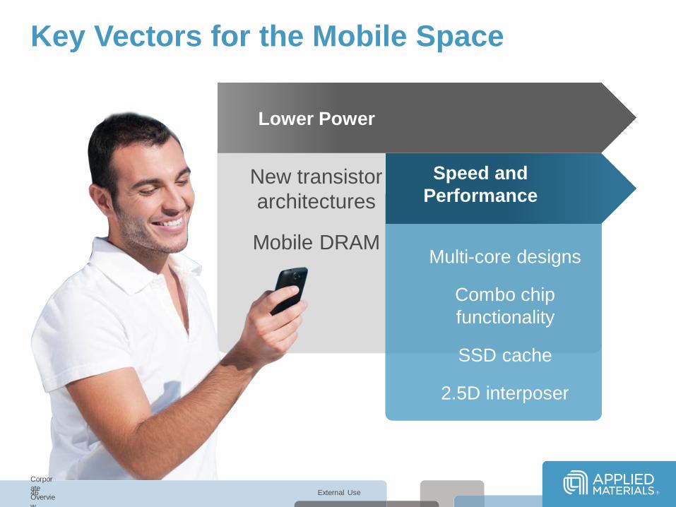
Key Vectors for the Mobile Space
New transistor architectures
Mobile DRAM Multi-core designs
Combo chip functionality
SSD cache
2.5D interposer
Speed and Performance
Lower Power
46
Corporate Overview

External Use
Mobility Demands Ultra-Low Chip Power
47
All day battery life
Idle power
Instant on
New form factors
Always connected
Active power
High definition displays
Video playback
Multi-tasking
Audio playback
Eight hours talk time
One week standby time

External Use
Large Screen TV
Laptop PC
Mobility Creating “Fourth Wave” in Displays
Smart Phones and Tablets
Desktop Monitor
48

External Use
Opportunities in Mobile Displays
Smartphones and tablets
Hi-resolution LCD
OLED
Smartphone to large and 3D
Touch everything
E-reader
49
Corporate Overview

External Use
Solar Learning Curve Accelerating
50
$/Wp
Cumulative Installations (GW)
Source: Navigant Consulting, NREL, Solarbuzz, pvXchange, Morgan Stanley, New Energy Finance
BALANCE OF SYSTEMS
COST
AVERAGE MODULE
COST
END CY11 70GW
Corporate Overview

External Use
Business Segments
Display Energy and Environmental
Solutions
Semiconductor Applied Global Services
51 Corporate Overview

External Use
Global leader in innovative equipment for the manufacture of advanced semiconductors
Systems are mainstay of virtually every advanced semiconductor factory
Leading position in majority of advanced chip processes
Launched 16 new products in 2011
52
Corporate Overview
Semiconductor
* Source: Gartner, April 2011
Global expansion of consumer base will drive demand for mobile PCs, smart phones and other
types of consumer electronics

External Use
Accelerating Innovation
Thermal
Metals
Deposition
Planarization
Etch Inspection
Corporate Overview 53
Collaborate earlier and deeper with customers on inflections
Provide the broadest suite of solutions with unmatched integration benefits
Drive to atomic precision on interfaces with multi-chamber platforms
Extend the technology roadmap with fast cadence in product innovation
Enable faster learning with Maydan Technology Center
Plating Implant
This image cannot currently be displayed.
This image cannot currently be displayed.
This image cannot currently be displayed.

External Use
#1 in TFT-LCD equipment and services
Extending core equipment technology into new mobility
segments
The equipment we build uses scale to help make flat panel
TVs more than 20% larger each year without price increase
Display
54
Corporate Overview
* Source: Gartner, April 2011
Exploring emerging display technologies, such as touch panel, flexible substrate and OLED which will
drive the future of the screen

External Use
55
Corporate Overview
Expanding Portfolio to Grow in New Segments
TV
Monitor and Notebook
Mobile phone PVD Array
PVD Color Filter
PiVot™
New Aristo Color Filter
KPX CVD
CVD Metal Oxide PiVot Metal Oxide
ADAPTING
Core Applications
Applied Materials Products
Major End Products
Display Product Landscape
Tablet
Smart Phone
Other High-performance Mobile
New TV + LTPS
+ Touch
CVD Array PECVD
Array Test EBT
+ Metal Oxide
New Aristo Touch Panel PVD SmartWeb®
Core TFT-LCD Equipment
New Equipment Segments

External Use
Energy and Environmental
Solutions
56
Corporate Overview
* Source: VLSI Research 2010
Energy Conversion
Energy Conservation
Energy Storage
#1 PV Equipment Provider*
Powering the c-Si Roadmap Driving down cost/watt and balance
of system (BOS)
• Advanced cell technologies • Both scale and technology
• Greater efficiency • Lower production costs
• Grid parity Accelerating global photovoltaic (PV) adoption by delivering cost-effective solutions that integrate technology, equipment and materials to improve factory productivity and increase
cell efficiency.

External Use
PV Manufacturing Solutions Leadership
57
Silicon Ingot Wafer Cell Module
Increased cell efficiencies
Higher productivity
Advanced automation
Advanced Vision System
Modular platform
Best in class yield
Highest productivity
Thinner wafers
Consumables reduction
Upgradeable platform
Applied Baccini™ Cell Systems Applied HCT Wafering Systems
Corporate Overview
#1 Equipment Provider
Source: Ranked by VLSI

External Use
Applied Global Services
58
Corporate Overview
Helping customers lower costs, improve equipment and fab performance and maximize
return on assets
Broad, flexible portfolio for custom solutions
Advanced predictive and diagnostic technologies
Innovative technology extension and conversion
World-class expertise and knowledge-base systems
Optimizing efficiency of semiconductor, display and solar factories through integrated services,
spares, equipment and automation software.

External Use
Applied Global Services Service, Equipment & Automation Software
59
FAB SERVICES Supporting > 30,000 tools with ~3,000 field engineers Innovative, flexible service solutions
FabVantage™ benchmarking and assessments
EQUIPMENT 200mm semi, legacy solar and display, Subfab dedicated R&D for emerging technology applications, Comprehensive technology, productivity upgrades
FACTORY AUTOMATION SOFTWARE Manufacturing Execution Systems (MES) Equipment and Process Control (EES)
Batch Scheduling (SmartSched™)
Corporate Overview

External Use
We’re ready for incredible things. Whatever the next breakthrough,
we are ready to provide the manufacturing solutions to make
innovative ideas a reality.
Delivering Essential Technology for a Competitive Advantage
60 Corporate Overview

External Use
Turning Innovations into Industries™
Presenter Name email address Learn more. Visit amat.com

External Use
0
20
40
60
80
100
120
1995 1997 1999 2001 2003 2005 2007 2009 2011F 2013F
TFT-
LCD
Indu
stry
Rev
enue
($B
)
Source: Display Search, AKT
Gen 3
Gen 4
Gen 5/6
Gen 7
Gen 8.5
4th Wave
Laptop PC
1st Wave
Large Screen TV
3rd Wave 2nd Wave
Desktop Monitor
Gen 10
Mobility
New Environment • Mobility Focus • No Gen Scaling • Multiple Smaller Gens • New Technologies • Apple Influence • Increasing Touch!
Evolution of the Display Industry
62

External Use
Exciting Times for PCT
63
Apple iPad2
Dell 17” touch notebook iPhone 4
Retina LCD Amazon Kindle Galaxy
4.3” OLED
Samsung 7” Galaxy Tab
Nintendo 3DS Mobile 3D w/o Glasses
Nintendo 3DS
Evolution of PCT Driven by: Cost Reduction Weight & Thickness Reduction Optical Appearance
Improvement Reduced Energy Consumption

External Use
Supporting a Multi-Player Value Chain
Touch Panel Value Chain
Source (value chain): Cypress Perform, 2008
New Aristo PVD a-Si & LTPS PECVD
SmartWeb PVD
Applied SSG
64

External Use
Key Vectors for the Mobile Space
New transistor architectures
Mobile DRAM Multi-core designs
Combo chip functionality
SSD cache
2.5D interposer
Speed and Performance
Lower Power
65

External Use
Mobility Demands Ultra-Low Chip Power
66
All day battery life
Idle power
Instant on
New form factors
Always connected
Active power
High definition displays
Video playback
Multi-tasking
Audio playback
Eight hours talk time
One week standby time

External Use
Opportunities in Mobile Displays
67
MOBILE High-resolution Thin and light Low power Interactivity
External Use
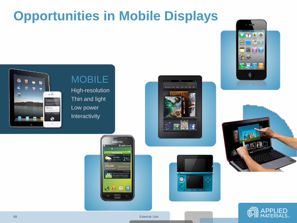
Opportunities in Mobile Displays
68
MOBILE High-resolution Thin and light Low power Interactivity

External Use
Growth Led by Projective Capacitive TP
Total Area CAGR ~ 23% Projective Capacitive Touch Panel CAGR ~ 35%
– By 2017, Projective Capacitive May Account for ~70% of Total Area
69
Source: DisplaySearch, July 2011
Key Driver of Growth Cost Reduction!

External Use
Projective Capacitive Touch Panel Construction
– Touch changes dielectric environment of x-y-capacitor
– Some E-field lines are ”projected“ beyond the cover sheet
Size: 3.5“ to 30“
Advantages – High durability and high optical quality – Multi-touch capability – Unaffected by surface debris or
contamination
Disadvantages – High cost touch technology – Finger or tethered pen use only
Market Trends – Mobile, tablet and high end devices – Rapidly increasing market penetration
70

External Use
End Market Requirements Driving New Display Technology Adoption
71
LTPS 2X TV Large size High-resolution Vivid color 3D Value
MOBILE High-resolution Thin and light Low power Interactivity
TECHNOLOGY SOLUTIONS
α-Si LCD
High-res LCD
OLED
TRANSISTOR SOLUTIONS
Metal Oxide 1.3X
EQUIPMENT OPPORTUNITY
(vs. a-Si)

External Use
Touch Sensor Technology Concepts