robust design of unearthed single-electrode teng from three
TRANSCRIPT

Contents lists available at ScienceDirect
Nano Energy
journal homepage: www.elsevier.com/locate/nanoen
Robust design of unearthed single-electrode TENG from three-dimensionally hybridized copper/polydimethylsiloxane film
Meng Zhanga, Yang Jiea,b, Xia Caoa,b,⁎, Jie Biand, Tao Lia, Ning Wangd,⁎, Zhong Lin Wanga,c,⁎
a Beijing Institute of Nanoenergy and Nanosystems, Chinese Academy of Sciences, National Center for Nanoscience and Technology (NCNST), Beijing100083, Chinab School of Chemistry and Biological Engineering, University of Science and Technology Beijing, Beijing 100069, Chinac School of Material Science and Engineering, Georgia Institute of Technology, Atlanta, GA 30332-0245, United Statesd Center for Green Innovation, School of Mathematics and Physics, University of Science and Technology Beijing, Beijing 100069, China
A R T I C L E I N F O
Keywords:Cu-PDMS filmUnearthedSingle-electrode modeTriboelectric nanogeneratorIntegrated electrochromic film
A B S T R A C T
Developing novel smart materials for the next generation of advanced electronic devices represents a majorchallenge as well as an exciting opportunity in the direction of integration, miniaturization, and flexibility. Herean unearthed single-electrode triboelectric nanogenerator (TENG) is fabricated from three-dimensionallyhybridized copper/polydimethylsiloxane powering films. This robust design simplifies the traditional contact-separation mode so that the as-fabricated single-electrode TENG is simple, stable, waterproof and can beoperated without grounding. The output current reaches 1.2 μA cm−2 when a pressure as small as 5 N cm−2 isapplied, which leads to the invention of a pressure sensitive device by integrating with an electrochromic film.The pioneering unearthed single-electrode working modes start up a multifunctional platform for both energyharvesting and self-powered touch sensors.
1. Introduction
Currently electrochemical cells such as Li-ion batteries dominatethe market of electrochemical power sources for portable electricalapparatus while the constant expansion of intelligent applicationsstepped up the demands for much higher energy-density [1,2]. Thus,efficiently miniaturized electrical devices for energy delivery or harvest-ing with high-performance are urgently needed because they canprovide almost inexhaustible power by converting ambient energiesinto electricity [3]. However, up to now, most of such converters arebased on electromagnetic induction effect, which are usually bulky andcomplex [4–7]. As a result, portable, cost-effective and flexibleapproaches that can directly harvest mechanical energy for publicutilities become the hot favorite.
Triboelectric nanogenerators (TENGs) are a type of electronicdevices that can efficiently convert ambient mechanical energy suchas human activities, tire rotation, ocean waves and mechanical vibra-tion into electricity via triboelectric and electrostatic induction effects[3,6]. At present, TENGs have been widely used in trace memory
systems [8], self-charging cells [9], distress signal emitters [10], self-electroplating technology [11] and self-powered sensors [10,12–19].The state-of-art TENGs are generally built in contact-separation modeand composed of two electrodes with different surface potentials, whichnot only demands complicated process and precise operations, but alsolargely limits the applications in some tough conditions owing to thepackaging issues [3,15,20,21]. For self-powered electrochemicalsystem, stable structure, simple fabrication, low expense andhigh performance are indispensable for smart electronic integration[22–29]. Accordingly, design optimization on the structure andelectronic system is a key approach to improve the output performance[30,31].
In this work, we demonstrated the robust design of unearthedsingle-electrode TENG (referred as h-TENG) made from copper foamand interlaced porous PDMS film (referred as CPDMS film). The as-fabricated one-chip h-TENG exhibits high mechanical durability,excellent stability and overall water resistance. Self-powered electro-chromic device has also been explored by integration with PDLC(polymer dispersed liquid crystal), which can be utilized as intelligent
http://dx.doi.org/10.1016/j.nanoen.2016.10.002Received 18 July 2016; Received in revised form 3 October 2016; Accepted 4 October 2016
⁎ Corresponding authors at: Beijing Institute of Nanoenergy and Nanosystems, Chinese Academy of Sciences, National Center for Nanoscience and Technology (NCNST), Beijing100083, China; University of Science and Technology Beijing, Beijing 100069, PR China.
E-mail addresses: [email protected] (X. Cao), [email protected] (N. Wang), [email protected] (Z.L. Wang).
Nano Energy 30 (2016) 155–161
2211-2855/ © 2016 Elsevier Ltd. All rights reserved.Available online 04 October 2016
crossmark

pressure sensors responding to tapping, pressing, treading and othermechanical movements.
2. Results and discussion
Morphology of the three-dimensional copper foam is shown inFig. 1a, and the schematic diagram of the h-TENG is shown in Fig. 1b.After hybridization, the sponge-like three-dimensional pores are filledwith PDMS film. Thickness of the h-TENG shown in Fig. 1c is of about1.77 mm, which can be further tuned by changing the thickness of thecopper foam. The cross-sectional view of the hybrid film demonstratesthe micro gap between the copper foam and PDMS film because of thehydrophobicity (Fig. 1d). Scheme of the fabrication of the h-TENG isshown in Fig. 1e.
As shown by Fig. S1a, PDMS films prepared from mixed PDMS/water suspension is inclined to develop spherical pores along with theremoval of the DI water because of the inherent hydrophobicity ofPDMS. The powering Cu/PDMS films were prepared by the dip-coatingmethod. It can be observed that PDMS infiltrates the copper foam andforms a sponge-like microstructure at this stage (Fig. S1a–d).Nevertheless, the conspicuous porosity in PDMS cannot be obtainedwithout DI water (referred as PDMS-np, Fig. S1b), nor with acetone ormethylene chloride (referred as PDMS-a/-m (Fig. S1c and d)). Theboiling point of acetone and dichloromethane is much lower incomparison with water. It may be deduced that the organic solventsevaporate too fast to form the micro voids during the curing of PDMS.In contrast, the moderate evaporation rate of water is beneficial to theformation of micro pores in the curing process, and water can act aseffective pore-making agent in large batch.
The electric properties of the h-TENGs are shown in Fig. 2. Theshort-circuit output current and the open-circuit output voltage are allmeasured under an acceleration of 3 m s−2, a running distance of63 mm and an external force of 15 N by a linear motor. It can be seenthat the hybrid film prepared with 50% wt DI water shows a muchhigher current output than the pure PDMS (Fig. 2a and b), and theoutput current reaches 1.2 μA cm−2 even a pressure as small as5 N cm−2 is applied (Fig. 2a). The voltage characterizations show asimilar trend as that of the current. As shown in Fig. 2c and d, theopen-circuit voltage of PDMS-p-based h-TENGs is much higher thanthat from the PDMS-np samples. It can be deduced the porousstructure increases the contact surface and obviously enhances the
output power of the h-TENG. In another test, film thickness doesn’tshow any obvious impact on output current of the h-TENG, as shownby Fig. 2e. Thus the film thickness is kept as 1.73 mm in this work. InFig. 2f, PDMS-a/-d/-n based h-TENGs show approximate short-circuitoutput currents, according with the observation that neither acetonenor methylene chloride can endow the composite material withconspicuous porosity due to their fast evaporation speed.
The ductility and soundness were tested by a linear motor with anacceleration of 3 m s−2, a running distance of 63 mm and an externalforce of 15 N. A steady output can be obtained from the h-TENG evenafter thousands of bending ( > 2000 cycle, > 50°), demonstrating itsgood flexibility and fatigue-resistance property (Fig. S2a and b). Incomparison with traditional TENGs, this porous h-TENG needn’t toattach any metal electrode and can work in conditions of high humiditydue to the excellent surface hydrophobic property. This featuredistinguished itself sharply from the traditional TENGs because theattached metal electrode for the latter is sensitive to moisture. In thewater-resistance experiment, the h-TENG was soaked with DI water forseveral hours. The output current (Fig. S2c) and the output voltage(Fig. S2d) are almost unchanged soon after it was taken out, demon-strating excellent water tolerance.
The most possible charge induction mechanism within the PDMS-p-based h-TENG is schematically shown in Fig. 3. Charges are resultedfrom the coupling of triboelectric effect and electrostatic induction, asdemonstrated by the controlled experiments [3,30–34]. Here theinterfacial charge dissipation model should be applied.Microscopically, when the h-TENG is squeezed, the copper foam andPDMS contact fully and friction occurs. Electrons are transferred fromcopper foam to PDMS film, resulting in positive charges on copperfoam and negative charges inside the pores of PDMS at the squeezedspot. As the force is withdrawn, the copper foam is partly separatedfrom PDMS film. On the other hand, we can always assume that thehybrid is uniform macroscopically though the elastic deformationcaused by applied stress is always asymmetric, which decreases sharplyalong with the distance from the pressure point. Thus statically, PDMSfilm at the force point is apt to be negative charge while positivecharges are always transported to bottom surface (assuming the forcepoint as the upper surface) regardless the position of the copper foamwithin the pores. Under short-circuit condition, electrons near thesqueezing spot move to far-end/bottom surface through an externalcircuit to neutralize the positive triboelectric charges, reaching an
Fig. 1. (a, b) SEM image and the schematic diagram of the copper foam. (c) The as-fabricated h-TENGs with different sizes. (d) Cross-sectional SEM image of the hybrid film. (e)Schematic illustration of the h-TENG.
M. Zhang et al. Nano Energy 30 (2016) 155–161
156

electrostatic equilibrium and generating a negative current signal.When the hybrid electrode fully reverts to the initial position, thereis no electron flowing through the circuit till the h-TENG is pressedagain. In this circle, the copper foam will contact with PDMS again,causing the charges to disappear, and charges decrease on both of thetop and bottom surface, which produces a downwards current.Therefore, electrons are driven from the non-contact pot/bottom layerback to contact spot/top layer, decreasing the amount of inducedcharges and leading to a positive current signal. At the end of the circle,copper foam and the PDMS inside the pores are in contact again and allinduced charges are neutralized.
Meanwhile, the single-wire transmission mode also contributes tothe charge generation at the skin-hybrid film interface (Fig. 4). Here
once a relative separation between Cu electrode and skin occurs,negative charges on the surface of the skin induce positive chargeson the Cu electrode, driving free electrons flowing from the far-end ofthe wire via the load (e.g., LEDs) to the Cu electrode (Fig. 4a–c). Whennegative triboelectric charges on the skin are fully screened from theinduced positive charges on the Cu electrode by increasing theseparation distance between the Cu and skin, no output signals canbe observed, as illustrated by Fig. 4d. Besides, when the skin wasreverted to approach the Cu electrode, the induced positive charges onthe Cu electrode increase and the positive charges in the wire will flowfrom the far end of the wire to the Cu electrode until the skin and Cufully contact with each other again, resulting in a reversed outputvoltage/current signal (Fig. 4e). This is another full cycle of the
Fig. 2. Output current of the h-TENGs prepared with (a) and without DI water (b). (c, d) Corresponding voltages of the h-TENG prepared with 50% /without DI water. (e) Outputcurrents of h-TENGs with different thickness. (f) Output currents of PDMS-a/PDMS-d based h-TENGs. The area of the as-prepared samples is 1 cm×3 cm.
M. Zhang et al. Nano Energy 30 (2016) 155–161
157
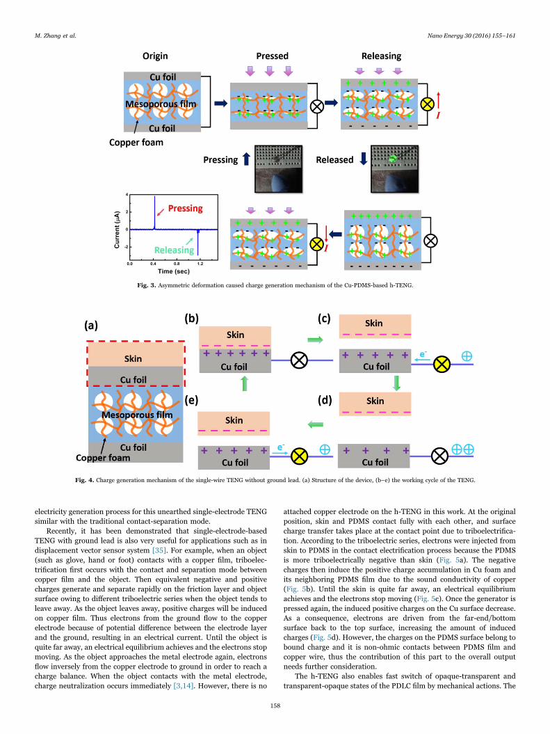
electricity generation process for this unearthed single-electrode TENGsimilar with the traditional contact-separation mode.
Recently, it has been demonstrated that single-electrode-basedTENG with ground lead is also very useful for applications such as indisplacement vector sensor system [35]. For example, when an object(such as glove, hand or foot) contacts with a copper film, triboelec-trification first occurs with the contact and separation mode betweencopper film and the object. Then equivalent negative and positivecharges generate and separate rapidly on the friction layer and objectsurface owing to different triboelectric series when the object tends toleave away. As the object leaves away, positive charges will be inducedon copper film. Thus electrons from the ground flow to the copperelectrode because of potential difference between the electrode layerand the ground, resulting in an electrical current. Until the object isquite far away, an electrical equilibrium achieves and the electrons stopmoving. As the object approaches the metal electrode again, electronsflow inversely from the copper electrode to ground in order to reach acharge balance. When the object contacts with the metal electrode,charge neutralization occurs immediately [3,14]. However, there is no
attached copper electrode on the h-TENG in this work. At the originalposition, skin and PDMS contact fully with each other, and surfacecharge transfer takes place at the contact point due to triboelectrifica-tion. According to the triboelectric series, electrons were injected fromskin to PDMS in the contact electrification process because the PDMSis more triboelectrically negative than skin (Fig. 5a). The negativecharges then induce the positive charge accumulation in Cu foam andits neighboring PDMS film due to the sound conductivity of copper(Fig. 5b). Until the skin is quite far away, an electrical equilibriumachieves and the electrons stop moving (Fig. 5c). Once the generator ispressed again, the induced positive charges on the Cu surface decrease.As a consequence, electrons are driven from the far-end/bottomsurface back to the top surface, increasing the amount of inducedcharges (Fig. 5d). However, the charges on the PDMS surface belong tobound charge and it is non-ohmic contacts between PDMS film andcopper wire, thus the contribution of this part to the overall outputneeds further consideration.
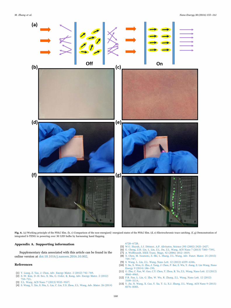
The h-TENG also enables fast switch of opaque-transparent andtransparent-opaque states of the PDLC film by mechanical actions. The
Fig. 3. Asymmetric deformation caused charge generation mechanism of the Cu-PDMS-based h-TENG.
Fig. 4. Charge generation mechanism of the single-wire TENG without ground lead. (a) Structure of the device, (b–e) the working cycle of the TENG.
M. Zhang et al. Nano Energy 30 (2016) 155–161
158

working mechanism of the PDLC film is depicted by Fig. 6a. In theabsence of any electric field, liquid crystal molecules are disorderlyarranged, showing the opaque state. On the contrary, liquid crystalmolecules in the PDLC film are arranged along the electric fielddirection and leads to the transparency of the PDLC film whenenergized. In this work, one piece of PDLC film was pasted onto theh-TENG surface to test its color change with an external pressure. Asshown in Fig. 6b and c, the PDLC film becomes transparent and thebottom object appears from the PDLC film when a slight pressure isapplied. As mentioned above, when a pressure is applied, an electricfield will be generated on the h-TENG owing to coupled inductiveeffect, making the PDLC film energized and showing the trace of thepressure temporally. When the pressure disappears, the electric field isabsent, and the trace is gone. The handwritten path on the PDLC filmcan then be captured in real-time for secure electronic signaturecollections (Fig. 6d and e). In the kinetic energy harvesting test, overthirty LED bulbs were lighten up upon slightly flapping the h-TENG(Fig. 6f and g). In this energy conversion process, the mechanicalmotion is not necessarily to be flat. It means that the h-TENG can beinstalled to the court, the plaza and even the subway as a stable powersupply.
3. Conclusion
In conclusion, a simple strategy for fabricating unearthed single-electrode h-TENGs from hybrid Cu-PDMS films has been demon-strated. The as-fabricated single-electrode h-TENGs are not only stableand waterproof, but also sensitive to vibration and pressure and can beintegrated into electrochromic devices for recording pressure trace.Thus this robust design represents a multifunctional platform for bothenergy harvesting and tribophototronics and can be used for interactivedisplay, integrated circuits, and flexible/touch optoelectronics.
4. Experimental section
The PDMS monomers and curing agent was mixed in a mass ratio
of 10:1 in a beaker. Deionized water (DI water) was then added toincrease the porosity. In a typical process flow, the copper foam wasfirst cleaned in an aqueous 1.0 M HCl solution for about 20 s, rinsedwith DI water, then dried under a N2 gas flow. In the controlledexperiment, DI water was replaced by acetone and methylene chlorideto tune the porosity of the film. Then the mixture was stirred for about30 min and kept in a vacuum chamber to remove the air remained inPDMS. To prepare the hybrid film, the copper foam was dipped into thePDMS suspension for three hours. Thickness of the films can becontrolled by repeating the dipping process. The hybrid CPDMS filmwas then placed on a SiO2/Si mold and solidified in atmosphere at90 °C for 1 h. The dried CPDMS film was peeled off from the substrate,thus a porous film was obtained.
The surface morphologies of the as-fabricated CPDMS film werecharacterized by a SU8020 field emission scanning electron microscope(SEM). The output voltage and current of the h-TENG were measuredby applying an external force with a commercial linear mechanicalmotor (Linmot Inc.). The reciprocating motion of the generator wastuned by the motor-controlling program. The friction between thePDMS film and the copper foam resulted in a triboelectric potential andan electrical output in the external circuit. A Keithley Model 6514System Electrometer was used to measure the open-circuit voltage,while we used an SR570 low-noise current amplifier (StanfordResearch System) to measure the short circuit current.
Acknowledgements
We acknowledge financial support from the National NaturalScience Foundation of China (NSFC Nos. 21275102, 21173017,51272011 and 21575009), the Science and Technology ResearchProjects from Education Ministry (213002A), National “Twelfth Five-Year” Plan for Science & Technology Support (No. 2013BAK12B06),the “Thousands Talents” Program for Pioneer Researcher and HisInnovation Team, China, and the National Natural Science Foundationof China (Grant Nos. 51432005 and Y4YR011001).
Fig. 5. (a–d) Electrostatically induced charge generation mechanism at the skin-h-TENG interface without attached electrodes. This is another configuration that we found that cangenerate electricity in practice.
M. Zhang et al. Nano Energy 30 (2016) 155–161
159
Appendix A. Supporting information
Supplementary data associated with this article can be found in theonline version at doi:10.1016/j.nanoen.2016.10.002.
References
[1] Y. Liang, Z. Tao, J. Chen, Adv. Energy Mater. 2 (2012) 742–769.[2] S.-W. Kim, D.-H. Seo, X. Ma, G. Ceder, K. Kang, Adv. Energy Mater. 2 (2012)
710–721.[3] Z.L. Wang, ACS Nano 7 (2013) 9533–9557.[4] S. Wang, Y. Xie, S. Niu, L. Lin, C. Liu, Y.S. Zhou, Z.L. Wang, Adv. Mater. 26 (2014)
6720–6728.[5] W.U. Huynh, J.J. Dittmer, A.P. Alivisatos, Science 295 (2002) 2425–2427.[6] G. Cheng, Z.H. Lin, L. Lin, Z.L. Du, Z.L. Wang, ACS Nano 7 (2013) 7383–7391.[7] A. Wolfbrandt, IEEE Trans. Magn. 42 (2006) 1812–1819.[8] X. Chen, M. Iwamoto, Z. Shi, L. Zhang, Z.L. Wang, Adv. Funct. Mater. 25 (2015)
739–747.[9] S. Wang, L. Lin, Z.L. Wang, Nano Lett. 12 (2012) 6339–6346.
[10] Y. Su, X. Wen, G. Zhu, J. Yang, J. Chen, P. Bai, Z. Wu, Y. Jiang, Z. Lin Wang, NanoEnergy 9 (2014) 186–195.
[11] G. Zhu, C. Pan, W. Guo, C.Y. Chen, Y. Zhou, R. Yu, Z.L. Wang, Nano Lett. 12 (2012)4960–4965.
[12] F.R. Fan, L. Lin, G. Zhu, W. Wu, R. Zhang, Z.L. Wang, Nano Lett. 12 (2012)3109–3114.
[13] Y. Jie, N. Wang, X. Cao, Y. Xu, T. Li, X.J. Zhang, Z.L. Wang, ACS Nano 9 (2015)8376–8383.
Fig. 6. (a) Working principle of the PDLC film. (b, c) Comparison of the non-energized/ energized states of the PDLC film. (d, e) Electrochromic trace catching. (f, g) Demonstration ofintegrated h-TENG in powering over 30 LED bulbs by harnessing hand flapping.
M. Zhang et al. Nano Energy 30 (2016) 155–161
160

[14] R.M. Yu, C.F. Pan, J. Chen, G. Zhu, Z.L. Wang, Adv. Funct. Mater. 23 (2013)5868–5874.
[15] F.R. Fan, Z.Q. Tian, Z.L. Wang, Nano Energy 1 (2012) 328–334.[16] Z. Li, J. Chen, J. Zhou, L. Zheng, K.C. Pradel, X. Fan, H. Guo, Z. Wen, M.-H. Yeh,
C. Yu, Z.L. Wang, Nano Energy 22 (2016) 548–557.[17] Y. Fang, J. Tong, Q. Zhong, Q. Chen, J. Zhou, Q. Luo, Y. Zhou, Z. Wang, B. Hu,
Nano Energy 16 (2015) 301–309.[18] X. Zhong, Y. Yang, X. Wang, Z.L. Wang, Nano Energy 13 (2015) 771–780.[19] Z. Wen, J. Chen, M.-H. Yeh, H. Guo, Z. Li, X. Fan, T. Zhang, L. Zhu, Z.L. Wang,
Nano Energy 16 (2015) 38–46.[20] A.F. Yu, Y. Zhao, P. Jiang, Z.L. Wang, Nanotechnology 24 (2013) 055501.[21] S.M. Niu, S.H. Wang, L. Lin, Y. Liu, Y.S. Zhou, Y.F. Hu, Z.L. Wang, Energy Environ.
Sci. 6 (2013) 3576–3588.[22] Z.H. Lin, Y.N. Xie, Y. Yang, S.H. Wang, G. Zhu, Z.L. Wang, ACS Nano 7 (2013)
4554–4560.[23] Z.H. Lin, G. Zhu, Y.S. Zhou, Y. Yang, P. Bai, J. Chen, Z.L. Wang, Angew. Chem. 52
(2013) 5065–5069.[24] Z. Li, J. Chen, J. Yang, Y. Su, X. Fan, Y. Wu, C. Yu, Z.L. Wang, Energy Environ. Sci.
8 (2015) 887–896.[25] Y.K. Pang, F. Xue, L.F. Wang, J. Chen, J.J. Luo, T. Jiang, C. Zhang, Z.L. Wang, Adv.
Sci. 3 (2016) 1500419.[26] Z.L. Wang, Faraday Discuss. 176 (2014) 447–458.[27] C. Zhang, W. Tang, C.B. Han, F.R. Fan, Z.L. Wang, Adv. Mater. 26 (2014)
3580–3591.[28] C. Zhang, T. Zhou, W. Tang, C.B. Han, L.M. Zhang, Z.L. Wang, Adv. Energy Mater.
4 (2014) 1301798.[29] S. Kim, M.K. Gupta, K.Y. Lee, A. Sohn, T.Y. Kim, K.S. Shin, D. Kim, S.K. Kim,
K.H. Lee, H.J. Shin, D.W. Kim, S.W. Kim, Adv. Mater. 26 (2014) 3918–3925.[30] A. Cherkasov, J. Chem. Inf. Comput. Sci. 43 (2003) 2039–2047.[31] Y.F. Hu, Y. Zhang, C. Xu, G. Zhu, Z.L. Wang, Nano Lett. 10 (2010) 5025–5031.[32] Z.C. Quan, C.B. Han, T. Jiang, Z.L. Wang, Adv. Energy Mater. 6 (2016) 1501799.[33] Y.L. Zi, J. Wang, S.H. Wang, S.M. Li, Z. Wen, H.Y. Guo, Z.L. Wang, Nat. Commun.
6 (2015) 8376–8383.[34] Z.L. Wang, Adv. Mater. 24 (2012) 280–285.[35] Y. Yang, H.L. Zhang, J. Chen, Q.S. Jing, Y.S. Zhou, X.N. Wen, Z.L. Wang, ACS Nano
(2013) 7342–7351.
Meng Zhang obtained her B.C. in polymer material andengineering from Dalian University of Technology (2014).Now she is doing her master degree at the Beijing Instituteof Nanoenergy and Nanosystems, Chinese AcademicScience. Her current research mainly focuses on materialdesign and synthesis, energy harvesting and fabrication ofdevices.
Yang Jie is currently a Ph.D. candidate of the ResearchCenter for Bioengineering and Sensing Technology at theUniversity of Science and Technology Beijing, and jointtraining at the Beijing Institute of Nanoenergy andNanosystems, Chinese Academy of Sciences. His researchinterests include electrochemical sensors and self-poweredmicro-/nano-systems.
Xia Cao is currently a distinguished professor atUniversity of Science and Technology Beijing, and aprofessor at Beijing Institute of Nanoenergy andNanosystems, Chinese Academy of Sciences. Her mainresearch interests focus on the energy materials, nanoelec-troanalytical chemistry, self-powered nano-biosensors andpiezoelectric sensors.
Bian Jie obtained her B.C. in Chemistry and ChemicalEngineering from Liaocheng University (2015). Now she isdoing her master degree at the Beijing University ofAeronautics and Astronautics. (BUAA) Her current re-search mainly focuses on modification of materials andenergy harvesting.
Tao Li received his B.C. in Material Chemistry (2011) andM.S. in Material Physic and Chemistry (2014) fromLanzhou University. Now he is a Ph.D. student at theBeijing Institute of Nanoenergy and Nanosystem, ChineseAcademic Science. His current research mainly focuses onenergy harvesting and fabrication of nanodevices.
Ning Wang obtained his Ph.D. from Beijing University ofAeronautics and Astronautics (BUAA) in 2008. He iscurrently a Professor of School of Mathematics andPhysics, University of Science and Technology Beijing.His research interest is to understand fundamental me-chanisms underlying experimentally observed phenomenawith specific focus on electrochemical interface.
Zhong Lin (Z.L) Wang received his Ph.D. from ArizonaState University in physics. He now is the Hightower Chairin Materials Science and Engineering, Regents’ Professor,Engineering Distinguished Professor and Director, Centerfor Nanostructure Characterization, at Georgia Tech. Dr.Wang has made original and innovative contributions tothe synthesis, discovery, characterization and understand-ing of fundamental physical properties of oxide nanobeltsand nanowires, as well as applications of nanowires inenergy sciences, electronics, optoelectronics and biologicalscience. His discovery and breakthroughs in developingnanogenerators established the principle and technologicalroadmap for harvesting mechanical energy from the en-
vironment and biological systems for powering a personal electronics. His research onself-powered nanosystems has inspired the worldwide effort in academia and industry forstudying energy for micro-nano-systems, which is now a distinct disciplinary in energyresearch and future sensor networks. He coined and pioneered the field of piezotronicsand piezophototronics by introducing piezoelectric potential gated charge transportprocess in fabricating new electronic and optoelectronic devices. Details can be found at:www.nanoscience.gatech.edu.
M. Zhang et al. Nano Energy 30 (2016) 155–161
161