risc-v external debug support version 0.11nov12 - sifive · risc-v external debug support version...
TRANSCRIPT

RISC-V External Debug Support
Version 0.11nov12
Tim Newsome <[email protected]>
November 12, 2016
Warning! This draft specification will change before being ac-cepted as standard, so implementations made to this draft specifica-tion will likely not conform to the future standard.
Contents
1 Introduction 5
2 About This Document 52.1 Structure . . . . . . . . . . . . . . . . . . . . . . . . . . . . . . . 52.2 Terminology . . . . . . . . . . . . . . . . . . . . . . . . . . . . . . 52.3 Register Definitions . . . . . . . . . . . . . . . . . . . . . . . . . . 5
2.3.1 Long Name (shortname, at 0x123) . . . . . . . . . . . . . 6
3 Background 6
4 Supported Features 6
5 System Overview 7
6 Debug Transport Module (DTM) 9
7 Debug Module( DM) 97.1 Debug Bus . . . . . . . . . . . . . . . . . . . . . . . . . . . . . . 107.2 System Bus . . . . . . . . . . . . . . . . . . . . . . . . . . . . . . 117.3 Debug Interrupt Block . . . . . . . . . . . . . . . . . . . . . . . . 117.4 Halt Notification Block . . . . . . . . . . . . . . . . . . . . . . . . 117.5 Debug ROM . . . . . . . . . . . . . . . . . . . . . . . . . . . . . 127.6 Debug RAM . . . . . . . . . . . . . . . . . . . . . . . . . . . . . 127.7 Reset Control . . . . . . . . . . . . . . . . . . . . . . . . . . . . . 137.8 Bus Access . . . . . . . . . . . . . . . . . . . . . . . . . . . . . . 137.9 Serial Ports . . . . . . . . . . . . . . . . . . . . . . . . . . . . . . 137.10 Security . . . . . . . . . . . . . . . . . . . . . . . . . . . . . . . . 14
1

7.11 Debug Module Debug Bus Registers . . . . . . . . . . . . . . . . 147.11.1 Control (dmcontrol, at 0x10) . . . . . . . . . . . . . . . . 147.11.2 Info (dminfo, at 0x11) . . . . . . . . . . . . . . . . . . . . 167.11.3 Authentication Data (authdata0, at 0x12) . . . . . . . . 187.11.4 Authentication Data (authdata1, at 0x13) . . . . . . . . 187.11.5 Serial Data (serdata, at 0x14) . . . . . . . . . . . . . . . 197.11.6 Serial Status (serstatus, at 0x15) . . . . . . . . . . . . . 197.11.7 System Bus Address 31:0 (sbaddress0, at 0x16) . . . . . 207.11.8 System Bus Address 63:32 (sbaddress1, at 0x17) . . . . 207.11.9 System Bus Data 31:0 (sbdata0, at 0x18) . . . . . . . . . 207.11.10 System Bus Data 63:32 (sbdata1, at 0x19) . . . . . . . . 217.11.11 Halt Notification Summary (haltsum, at 0x1b) . . . . . . 217.11.12 System Bus Address 95:64 (sbaddress2, at 0x3d) . . . . 227.11.13 System Bus Data 95:64 (sbdata2, at 0x3e) . . . . . . . . 227.11.14 System Bus Data 127:96 (sbdata3, at 0x3f) . . . . . . . . 23
7.12 Debug Module System Bus Registers . . . . . . . . . . . . . . . . 237.12.1 Clear Debug Interrupt (cleardebint, at 0x100) . . . . . 237.12.2 Set Halt Notification (sethaltnot, at 0x10c) . . . . . . . 257.12.3 Serial Info (serinfo, at 0x110) . . . . . . . . . . . . . . . 257.12.4 Serial Send 0 (sersend0, at 0x200) . . . . . . . . . . . . . 257.12.5 Serial Receive 0 (serrecv0, at 0x204) . . . . . . . . . . . 257.12.6 Serial Status 0 (serstat0, at 0x208) . . . . . . . . . . . . 26
8 RISC-V Debug 268.1 Hart IDs . . . . . . . . . . . . . . . . . . . . . . . . . . . . . . . . 268.2 Debug Mode . . . . . . . . . . . . . . . . . . . . . . . . . . . . . 268.3 Debug ROM Contents . . . . . . . . . . . . . . . . . . . . . . . . 278.4 dret Instruction . . . . . . . . . . . . . . . . . . . . . . . . . . . 278.5 Load-Reserved/Store-Conditional Instructions . . . . . . . . . . . 288.6 Core Debug Registers . . . . . . . . . . . . . . . . . . . . . . . . 28
8.6.1 Debug Control and Status (dcsr, at 0x7b0) . . . . . . . . 288.6.2 Debug PC (dpc, at 0x7b1) . . . . . . . . . . . . . . . . . . 308.6.3 Debug Scratch Register (dscratch, at 0x7b2) . . . . . . . 308.6.4 Privilege Level (priv, at virtual) . . . . . . . . . . . . . . 30
9 Trigger Module 319.1 Trigger Registers . . . . . . . . . . . . . . . . . . . . . . . . . . . 31
9.1.1 Trigger Select (tselect, at 0x7a0) . . . . . . . . . . . . . 319.1.2 Trigger Data 1 (tdata1, at 0x7a1) . . . . . . . . . . . . . 329.1.3 Trigger Data 2 (tdata2, at 0x7a2) . . . . . . . . . . . . . 339.1.4 Trigger Data 3 (tdata3, at 0x7a3) . . . . . . . . . . . . . 339.1.5 Match Control (mcontrol, at 0x7a1) . . . . . . . . . . . . 339.1.6 Instruction Count (icount, at 0x7a1) . . . . . . . . . . . 35
2

10 JTAG Debug Transport Module 3710.1 Background . . . . . . . . . . . . . . . . . . . . . . . . . . . . . . 3710.2 JTAG Connector . . . . . . . . . . . . . . . . . . . . . . . . . . . 3810.3 JTAG Registers . . . . . . . . . . . . . . . . . . . . . . . . . . . . 38
10.3.1 IDCODE (00001) . . . . . . . . . . . . . . . . . . . . . . . 3810.3.2 DTM Control (dtmcontrol, at 10000) . . . . . . . . . . . 4110.3.3 Debug Bus Access (dbus, at 10001) . . . . . . . . . . . . 4210.3.4 BYPASS (11111) . . . . . . . . . . . . . . . . . . . . . . . 44
A Debugger Implementation 45A.1 Debug Bus Access . . . . . . . . . . . . . . . . . . . . . . . . . . 45A.2 Debug RAM . . . . . . . . . . . . . . . . . . . . . . . . . . . . . 45A.3 Main Loop . . . . . . . . . . . . . . . . . . . . . . . . . . . . . . 45A.4 Reading Memory . . . . . . . . . . . . . . . . . . . . . . . . . . . 46A.5 Writing Memory . . . . . . . . . . . . . . . . . . . . . . . . . . . 47A.6 Halt . . . . . . . . . . . . . . . . . . . . . . . . . . . . . . . . . . 47A.7 Reading Registers . . . . . . . . . . . . . . . . . . . . . . . . . . 49A.8 Writing Registers . . . . . . . . . . . . . . . . . . . . . . . . . . . 49A.9 Running . . . . . . . . . . . . . . . . . . . . . . . . . . . . . . . . 49A.10 Single Step . . . . . . . . . . . . . . . . . . . . . . . . . . . . . . 49A.11 Handling Exceptions . . . . . . . . . . . . . . . . . . . . . . . . . 50
B Debug ROM Source 50
C Trace Module 52C.1 Trace Data Format . . . . . . . . . . . . . . . . . . . . . . . . . . 53C.2 Trace Events . . . . . . . . . . . . . . . . . . . . . . . . . . . . . 53C.3 Synchronization . . . . . . . . . . . . . . . . . . . . . . . . . . . . 53C.4 Trace Registers . . . . . . . . . . . . . . . . . . . . . . . . . . . . 56
C.4.1 Trace (trace, at 0x728) . . . . . . . . . . . . . . . . . . . 56C.4.2 Trace Buffer Start (tbufstart, at 0x729) . . . . . . . . . 58C.4.3 Trace Buffer End (tbufend, at 0x72a) . . . . . . . . . . . 58C.4.4 Trace Buffer Write (tbufwrite, at 0x72b) . . . . . . . . . 58
D Future Ideas 58D.1 Lightweight Brainstorming . . . . . . . . . . . . . . . . . . . . . . 59
E Change Log 60
List of Figures
1 RISC-V Debug System Overview . . . . . . . . . . . . . . . . . . 8
3

List of Tables
1 Register Access Abbreviations . . . . . . . . . . . . . . . . . . . . 62 Debug Module Debug Bus Space . . . . . . . . . . . . . . . . . . 103 Debug Module System Bus Space . . . . . . . . . . . . . . . . . . 114 Debug Module Debug Bus Registers . . . . . . . . . . . . . . . . 145 Debug Module System Bus Registers . . . . . . . . . . . . . . . . 246 Debug ROM Contents . . . . . . . . . . . . . . . . . . . . . . . . 277 Core Debug Registers . . . . . . . . . . . . . . . . . . . . . . . . 288 Privilege Level Encoding . . . . . . . . . . . . . . . . . . . . . . . 309 Trigger Registers . . . . . . . . . . . . . . . . . . . . . . . . . . . 3110 JTAG Connector Diagram . . . . . . . . . . . . . . . . . . . . . . 3811 JTAG Connector Pinout . . . . . . . . . . . . . . . . . . . . . . . 3912 JTAG TAP Registers . . . . . . . . . . . . . . . . . . . . . . . . . 4013 Memory Read Timeline . . . . . . . . . . . . . . . . . . . . . . . 4814 Trace Sequence Header Packets . . . . . . . . . . . . . . . . . . . 5415 Trace Data Events . . . . . . . . . . . . . . . . . . . . . . . . . . 5516 Trace Registers . . . . . . . . . . . . . . . . . . . . . . . . . . . . 56
4

Acknowledgments
I would like to thank the following people for their time, feedback, and ideas:Bruce Ableidinger, Krste Asanovic, Mark Beal, Monte Dalrymple, Peter Egold,Gajinder Panesar, Klaus Kruse Pedersen, Antony Pavlov, Ken Pettit, MeganWachs, Stefan Wallentowitz, Ray Van De Walker, Andrew Waterman, and AndyWright.
1 Introduction
Software contains bugs, and to help find these bugs it is critical to have gooddebugging tools. Unless a robust OS is running on a core, with convenientaccess to it (eg. over a network interface), hardware support is required toprovide visibility into what is going on in that core. This document outlineshow that support should be provided on RISC-V platforms.
2 About This Document
2.1 Structure
This document contains two parts. The main part of the document is thespecification, which is given in the numbered sections. The second part of thedocument is a set of appendices. The information in the appendix is intendedto clarify and provide examples, but is not part of the actual specification.
2.2 Terminology
A platform is a single integrated circuit consisting of one or more components.Some components may be RISC-V cores, while others may have a differentfunction. Typically they will all be connected to a single system bus. A singleRISC-V core contains one or more hardware threads, called harts.
2.3 Register Definitions
All register definitions in this document follow the format shown in Section 2.3.1.A simple graphic shows which fields are in the register. The upper and lower bitindices are shown to the top left and top right of each field. The total numberof bits in the field are shown below it.
After the graphic follows a table which for each field lists its name, de-scription, allowed accesses, and reset value. The allowed accesses are listed inTable 1.
5

Table 1: Register Access AbbreviationsR Read-only.R/W Read/Write.R/W0 Read/Write. Only writing 0 has an effect.R/W1 Read/Write. Only writing 1 has an effect.W Write-only. When read this field returns 0.W1 Write-only. Only writing 1 has an effect.
2.3.1 Long Name (shortname, at 0x123)
31 8 7 0
0 field24 8
Field Description Access Resetfield Description of what this field is used for. R/W 15
3 Background
There are two forms of external debugging. The first is halt mode debugging,where an external debugger will halt some or all components of a platform andinspect them while they are in stasis. Then the debugger can allow the hardwareto either perform a single step or to run freely.
The second is run mode debugging. In this mode there is a software debugagent running on a component (eg. triggered by a timer interrupt on a RISC-V core) which communicates with a debugger without halting the component.This is essential if the component is controlling some real-time system (likea hard drive) where halting the component might lead to physical damage. Itrequires more software support (both on the chip as well as on the debug client).For this use case the debug interface may include simple serial ports.
A third use for the external debug interface is to use it as a general transportfor a component to communicate with the outside world. For instance, it couldbe used to implement a serial interface that firmware could use to provide asimple CLI. This can use the same serial ports used for run-mode debugging.
4 Supported Features
The debug interface described out here supports the following features:
1. RV32, RV64, and future RV128 are all supported.
2. Any hart in the platform can be independently debugged.
3. Harts can be asked to run a short custom program and immediately returnto regular execution afterwards, enabling relatively unintrusive inspectionof state.
6
4. Optionally, a bus master can be implemented to allow memory accesswithout involving any hart.
5. Debugging can be supported over multiple transports.
6. Code can be downloaded efficiently.
7. Each hart can be debugged from the very first instruction executed.
8. A RISC-V core can be halted when a software breakpoint instruction isexecuted.
9. Hardware can step over any instruction.
10. A RISC-V core can be halted when a trigger matches the PC, read/writeaddress/data, or an instruction opcode.
11. The debug module may implement serial ports which can be used forcommunication between debugger and monitor, or as a general protocolbetween debugger and application.
12. Arbitrary instructions can be executed on a halted hart. That means nonew debug functionality is needed when a core has custom instructions orregisters, as long as there exist programs that can store those registers tomemory.
13. The debugger doesn’t need to know anything about the microarchitectureof the cores it is debugging.
14. Minimizes the additional datapath needed in the core to implement debugfunctionality.
15. Don’t need to route a special debug bus to each core.
16. Cores don’t have to become bus slaves.
5 System Overview
Figure 1 shows the main components of External Debug Support. Blocks shownin dotted lines are optional.
The user interacts with the Debug Host, which is running a debugger. Thedebugger communicates with a Debug Translator (which may include a hard-ware driver) to communicate with Debug Transport Hardware that’s connectedto the host. The Debug Transport Hardware connects the Debug Host to thePlatform’s Debug Transport Module (DTM). The DTM provides access to theDebug Module (DM) which contains much of the debug functionality. Thisinterface is called the Debug Bus.
The DM allows the debugger to interrupt any hart in the platform. Whena running RISC-V core is interrupted, it enters Debug Mode and jumps to the
7
Figure 1: RISC-V Debug System Overview
8
Debug ROM. Generally this will cause it to execute code which has been writtento the Debug RAM. The debugger can use this mechanism to access memoryand registers at the cost of briefly halting one of the cores, or it can halt thehart and leave it halted.
Each RISC-V core may implement up to one Trigger Module for each hart.These can detect breakpoints as a hart is executing, which causes a hart to haltspontaneously. When that happens it notifies the DM by communicating overthe System Bus. The DM tracks the hart status, and makes it available in itsDebug Bus accessible registers so the debugger knows action is required. Thedebugger can then write appropriate instructions to Debug RAM, and send thehart another interrupt to indicate it should now jump to Debug RAM. Thisprocess is repeated until the debugger writes the code that causes the hart toleave Debug Mode.
Almost all this logic can be encoded in the Debug ROM. When a hart entersDebug Mode all it does is change the privilege mode it’s running in, and jumpto the beginning of Debug ROM. Code in the Debug ROM determines the causeand then either jumps straight to Debug RAM or notifies the debugger and thenwaits for further input from the debugger.
6 Debug Transport Module (DTM)
Debug Transport Modules provide access to the DM over one or more transports(eg. JTAG or USB).
There may be multiple DTMs in a single platform. Ideally every componentthat communicates with the outside world includes a DTM, allowing a plat-form to be debugged through every transport it supports. For instance a USBcomponent could include a DTM. This would trivially allow any platform to bedebugged over USB. All that is required is that the USB module already in usealso has access to the Debug Bus.
Using multiple DTMs at the same time is not supported. It is left to theuser to ensure this does not happen.
7 Debug Module( DM)
The Debug Module contains the shared functionality required to debug a RISC-V hart. It is accessed over two distinct buses that provide access to distinctregister sets. DTMs communicate with the DM using the Debug Bus. Hartscommunicate with the DM using the System Bus. In addition, the DM drivesindependent reset and interrupt signals to every hart.
A single DM can debug up to 1024 harts. If more harts need to be accessiblethe best solution is to extend the specification.
9

7.1 Debug Bus
The Debug Bus uses between 5 and 32 address bits, and 34 data bits. It supportsboth read and write operations. The bottom of the address space is used forthe DM. Extra space can be used for custom debug devices, other cores, etc.The space is laid out so that small to medium platforms can get away with just5 address bits, while DTMs used on large systems will want to use 6 bits. 7bits are only required for systems that want to use a large Debug RAM or haveother debug modules. Details of this bus are implementation-specific.
The registers are 34 bits wide so that simple DTMs can access every-thing that is essential for efficient operation in a single access. This keepsthe DTM simple, at the cost of a slightly awkward bus width. 34 bits areessential for an efficient bus master interface. The serial interface couldwork with 33 bits by jumping through some hoops involving special datavalues. The Debug RAM interface could actually work fine with just 33bits, but it’s worth to having extra bit just to make the (hopefully common)bus master extension great.
How this bus is implemented is completely left up to the designer, but inlarger systems it makes sense to use a standard multi-master bus. TODO:Recommend a specific bus.
Table 2 shows the layout of the Debug Bus address space.
Table 2: Debug Module Debug Bus SpaceAddress Description0x00 – 0x0f 64 bytes of R/W Debug RAM access. Each unique address
accesses 32 bits of the debug RAM, so 0x0 contains the firstword, 0x1 the second word, and so on.Bit 32 of every register provides R/W0 access to the haltnotification of the hart selected by hartid in dmcontrol. Bit33 of every register provides R/W1 access to the debuginterrupt of the hart selected by hartid in dmcontrol.
0x10 – 0x1b Debug Module registers described in Section 7.11.0x1c – 0x3b Halt Notification Status registers. Bit 0 of the first register
contains halt notification 0, while bit 31 of the last registercontains halt notification 1023 (if there are that many hartsattached).
0x3c – 0x3f Debug Module registers described in Section 7.11.0x40 – 0x6f 192 more bytes of R/W Debug RAM access for words 0x10 –
0x3f of the Debug RAM. Only implemented if Debug RAMis larger than 64 bytes. This spec doesn’t present anycompelling reason to implement that much Debug RAM.
Some registers might not be present, either because the feature they supportdoesn’t exist or because there’s simply empty space in the register map. Those
10

registers always read as 0, and writes to them are ignored.
7.2 System Bus
Harts being debugged communicate with the DM over the System Bus. TheDebug Module addresses are fixed across all platforms to reduce the amount ofcustomization required. Table 3 shows which address ranges are handled by theDM.
The debug registers and RAM are placed below 0x800 so that it ispossible to access the debug space relative to x0, which allows the DebugROM code to only save a single register upon entry.
Table 3: Debug Module System Bus SpaceAddress Description0x0 – 0xff Reserved for custom use.0x100 – 0x2ff Debug Module registers described in Section 7.12.0x400 – 0x4ff Up to 256 bytes of Debug RAM. Each unique address
specifies 8 bits.0x800 – 0x9ff Up to 512 bytes of Debug ROM.
This reliance on the System Bus means that debugging is not possible if theSystem Bus is hung for some reason. If this is a concern, then it’s possible toimplement a separate bus that allows each hart to access the registers listed inTable 3.
7.3 Debug Interrupt Block
This block controls interrupts from the Debug Module to a hart. It is used tohalt a currently running hart, or to signal that the hart should take an actionwhen it is already halted.
For each hart the block contains a single bit that gets set when 1 is writtento interrupt in dmcontrol or Debug RAM registers. The bit gets cleared whenits hart id is written to cleardebint. It is unspecified what happens if the bitis set and cleared at the same time.
The Debug Module conceptually has a direct connection to the debug inter-rupt signal of every hart that has one. Each hart must receive a signal changein no longer than 1 second. (How this is implemented is not further specified.A few clock cycles will be more typical.)
7.4 Halt Notification Block
This block tracks halt notifications from a hart to the Debug Module. It is usedby harts to inform the Debug Module that they halted for a reason other thanthe Debug Interrupt being asserted.
11

For each hart, the block contains a single bit that gets set when the cor-responding number is written to sethaltnot. The bit can be cleared usinghaltnot in dmcontrol and Debug RAM registers. It is read over the Debug Bususing haltsum, the halt notification section in the Debug Bus address space,and haltnot in dmcontrol and Debug RAM registers. It is unspecified whathappens if the bit is set and cleared at the same time.
It’s expected that a hart will write its hart ID to sethaltnot when it haltsspontaneously. (Debug ROM code takes care of this.) Any other writes willlikely confuse the debugger and should be avoided.
7.5 Debug ROM
The Debug ROM contains code for a RISC-V hart to execute when it entersDebug Mode. This ROM is inside the Debug Module so that it can be sharedamong all RISC-V harts in the system, and reduces the number of changesrequired to a RISC-V core to support debugging.
It is described in detail in Section 8.3.
7.6 Debug RAM
The Debug RAM is used by the debugger and the Debug ROM code to executearbitrary instructions, and to hold data. Debug RAM must be at least 28 bytesto accommodate 32-bit RISC-V cores, 40 bytes to accommodate 64-bit RISC-Vcores, and 64 bytes to accommodate 128-bit RISC-V cores.
Debug RAM is accessible over both the Debug Bus and the System Bus.When it is accessed by both simultaneously, reads may return undefined data,while writes may be ignored. If an access over the Debug Bus fails in this way,the result must be 2 (fail).
The minimum Debug RAM size is determined by the smallest debugprogram that can write an arbitrary value to an arbitrary location in RAM.That program consists of 4 instructions, followed by 3 XLEN-bit values(address, data, and scratch). Code for this program is shown in Sec-tion A.5. (When the compressed ISA is supported it would be possibleto cut 8 bytes from this requirement, but a debugger may assume that itdoesn’t need to use the compressed ISA.)
Since Debug RAM resides on the System Bus, it’s possible for any componentto write to it at any time. Unexpected writes should only happen when acomponent malfunctions, but if it does happen it will definitely interfere withdebugging. At the cost of more hardware, this can be resolved in two ways. Ifthe bus knows an ID for the originator, then the Debug Module can refuse writeaccesses to originators that don’t match the hart ID set in hartid of dmcontrol.If that’s not feasible, a more expensive option is to include a separate DebugRAM per hart, which is only accessible from that hart. To achieve this youwould likely need a separate bus that gives the DM full access and the harts
12

access to just their Debug RAM. hartid controls which Debug RAM the DMaccesses. This is an expensive solution, but still a valid implementation of thisspec.
7.7 Reset Control
This block is connected to global reset signals. The first signal resets everycomponent in the platform. The second signal is optional and resets the non-debug portion of every component in the platform. Both resets exclude anyDTMs and the Debug Module itself.
7.8 Bus Access
In a minimal configuration a debugger can access the system bus by having aRISC-V hart perform the accesses it requires. Optionally a Bus Access blockmay be implemented. Because the Bus Access block performs accesses directlyfrom the DM, it only uses physical addresses.
Implementing a Bus Access block has several benefits. First, it is now pos-sible to inspect a running system with minimal impact. The only impact nowis that the bus is busy while the debugger is performing an access. Second, itmay improve performance when downloading programs. There is only a benefitif JTAG TCK is a significant fraction of the RISC-V hart’s clock speed. Third,it may provide access to devices that a hart does not have access to. A hartmay be unable to access all devices in a system (eg. for security reasons) andin this case the debugger needs another path to access them.
To keep implementing, configuring, and using a debugger as simple as pos-sible, systems should use the same memory map for each hart. That meansthat a given address maps to the same device no matter which hart performsthe access. (Different harts may not all have permission to access the same de-vices.) If different harts do have unique memory maps then the system shouldprovide access to all devices using the Bus Access block. This will make imple-menting, configuring, and using a debugger more complex so should be avoidedif possible.
7.9 Serial Ports
The Debug Module may implement up to 8 serial ports. They support basic flowcontrol and full duplex data transfer between a component and the debugger.They can be used to communicate with a debug monitor running on a hart, forthe equivalent of printf debugging, to provide a simple CLI without requiringany extra peripherals, or more generally to emulate devices that aren’t present.All these uses require software support, and are not further specified here.
13

7.10 Security
To protect intellectual property it may be desirable to lock access to the DebugModule. To allow access during a manufacturing process and not afterwards, areasonable solution could be to add a fuse bit to the Debug Module that canbe used to be permanently disable it. Since this is technology specific, it is notfurther addressed in this spec.
Another option is to allow the DM to be unlocked only by users who havean access key. A simple mechanism is documented in Section 7.11. Whenauthenticated is clear, the DM must not interact with the rest of the platformin any way.
7.11 Debug Module Debug Bus Registers
Table 4: Debug Module Debug Bus RegistersAddress Name
0x10 Control0x11 Info0x12 Authentication Data0x13 Authentication Data0x14 Serial Data0x15 Serial Status0x16 System Bus Address 31:00x17 System Bus Address 63:320x18 System Bus Data 31:00x19 System Bus Data 63:320x1b Halt Notification Summary0x3d System Bus Address 95:640x3e System Bus Data 95:640x3f System Bus Data 127:96
7.11.1 Control (dmcontrol, at 0x10)
33 32 31 22 21 19 18 16
interrupt haltnot 0 buserror serial1 1 10 3 3
15 14 12 11 2 1 0
autoincrement access hartid ndreset fullreset1 3 10 1 1
14

Field Description Access Resetinterrupt This field contains the Debug Inter-
rupt bit for the hart selected by hartid.Writes apply to the new value of hartid.This field is also accessible when access-ing Debug RAM.
R/W1 0
haltnot This field contains the Halt Notifica-tion bit for the hart selected by hartid.Writes apply to the new value of hartid.This field is also accessible when access-ing Debug RAM.
R/W0 0
buserror When the debug bus master causes abus error, this field gets set. It remainsset until 0 is written to any bit in thisfield. Until that happens, the bus mas-ter is busy and no more accesses can beinitiated.0: There was no bus error.1: There was a timeout.2: A bad address was accessed.3: There was some other error (eg.alignment).
R/W0 0
serial Select which serial port is accessed byserdata.
R/W 0
autoincrement When 1, the internal address value(used by the bus master) is incrementedby the access size (in bytes) selected inaccess after every bus access.
R/W 0
access Select the access size to use for systembus accesses triggered by writes to thesbaddress registers or sbdata0.0: 8-bit1: 16-bit2: 32-bit3: 64-bit4: 128-bitIf an unsupported access size is writtenhere, the DM may not perform the ac-cess, or may perform the access with anyaccess size
R/W 2
hartid The ID of the hart to select. The haltnotification and debug interrupt of theselected hart are accessible in haltnotand interrupt in this register as well asevery Debug RAM register.
R/W 0
Continued on next page
15

ndreset Every time this bit is written as 1, ittriggers a full reset of the non-debuglogic on the platform. This bit existsso that, for debugging purposes, resetbehavior can be different from the stan-dard behavior. For instance, a corecould be forced into Debug Mode rightout of reset.
W1 0
fullreset Every time this bit is written as 1, ittriggers a full reset of the platform, in-cluding every component in it and thedebug logic for each component. It alsoresets the DM itself.
W1 0
7.11.2 Info (dminfo, at 0x11)
33 32 31 25 24 21 20 19 18
0 abussize serialcount access128 access64 access322 7 4 1 1 1
17 16 15 10 9 8 7 6
access16 access8 dramsize haltsum 0 loversion1 1 6 1 1 2
5 4 3 2 1 0
authenticated authbusy authtype loversion1 1 2 2
16

Field Description Access Resetabussize Width of the address bus in bits. (0 in-
dicates there is no bus access support.)R Preset
serialcount Number of supported serial ports. R Presetaccess128 1 when 128-bit bus accesses are sup-
ported.R Preset
access64 1 when 64-bit bus accesses are sup-ported.
R Preset
access32 1 when 32-bit bus accesses are sup-ported.
R Preset
access16 1 when 16-bit bus accesses are sup-ported.
R Preset
access8 1 when 8-bit bus accesses are supported. R Presetdramsize Size of the Debug RAM, in 32-bit words
minus 1. Eg. if Debug RAM is 32 bytes,it’s encoded here as 7 (32/4 − 1).A debugger must not access any De-bug RAM locations that fall outside therange specified here.
R Preset
haltsum 1 when haltsum is implemented. R Presetloversion Bits 3:2 of the 4-bit version field. R 0authenticated 0 when authentication is required be-
fore using the DM. 1 when the authen-tication check has passed. On compo-nents that don’t implement authentica-tion, this bit must be preset as 1.
R Preset
authbusy While 1, writes to authdata0 andauthdata1 may be ignored or may re-sult in authentication failing. Authen-tication mechanisms that are slow (orintentionally delayed) must set this bitwhen they’re not ready to process an-other write.
R 0
Continued on next page
17

authtype Defines the kind of authentication re-quired to use this DM.0: No authentication is required.1: A password is required.2: A challenge-response mechanism is inplace.3: Reserved for future use.
R Preset
loversion Bits 1:0 of the 4-bit version field. Thecombined version field is interpreted asfollows:0: There is no Debug Module present.1: There is a Debug Module and it con-forms to version 0.11 of this specifica-tion.Other values are reserved for future use.
R 1
7.11.3 Authentication Data (authdata0, at 0x12)
If authtype is 0, this register is not present.If authtype is 1, writing a correct password to this register and authdata1
enables the DM. The DM is disabled either by writing an invalid password, orby resetting it. 0 must not be used as a password. If an implementation wantsto use a well-known password, the recommended value is 0x5551212. Readingfrom the register returns 0.
If authtype is 2, things are a bit more complicated. Reading from the reg-ister pair reads the last challenge generated. Writing the correct response toauthdata1 and authdata0 enables the DM. The DM is disabled either by writ-ing an incorrect response, or by resetting it. Writing to authdata0 triggersvalidation, so if a 64-bit value is required then authdata1 must be written first.If the combined value in authdata0 and authdata1 is not a valid response afterwriting authdata0, then a new challenge must be generated. Depending on theimplementation, there may not be a valid challenge until the first write to thisregister.
33 32 31 0
0 data2 32
7.11.4 Authentication Data (authdata1, at 0x13)
This register contains the upper 32 bits of a 64-bit password or challenge/re-sponse as described in authdata0.
33 32 31 0
0 data2 32
18

7.11.5 Serial Data (serdata, at 0x14)
If serialcount is 0, this register is not present.All the fields in this register apply to the serial port selected by serial in
dmcontrol.
33 32 31 0
write/valid full/overflow data1 1 32
Field Description Access Resetwrite/valid Set this bit to write data to the
debugger-to-core queue.Read this bit to determine whether theregister contains valid data from thecore-to-debugger queue.
R/W 0
full/overflow 0: The debugger-to-core queue is notfull. The next write will be accepted.1: The debugger-to-core queue is cur-rently full, or the debugger has previ-ously attempted to write to the queuewhen it was full. To clear this state, thedebugger must write 0 to this bit. (Thequeue may still be full, in which case thebit will remain high.)
R/W0 0
data This field contains the oldest value inthe core-to-debugger queue if write/validreads as 1.
R/W 0
7.11.6 Serial Status (serstatus, at 0x15)
If serialcount is 0, this register is not present.
33 16 15 14 13 12 11
0 valid7 full/overflow7 valid6 full/overflow6 valid518 1 1 1 1 1
10 9 8 7 6 5
full/overflow5 valid4 full/overflow4 valid3 full/overflow3 valid21 1 1 1 1 1
4 3 2 1 0
full/overflow2 valid1 full/overflow1 valid0 full/overflow01 1 1 1 1
19

Field Description Access Resetvalid0 1 when the core-to-debugger queue for
serial port 0 is not empty.R 0
full/overflow0 full/overflow for serial port 0. R/W0 0
7.11.7 System Bus Address 31:0 (sbaddress0, at 0x16)
If abussize is 0, then this register is not present.
33 32 31 0
busy read address1 1 32
Field Description Access Resetbusy When 1, the bus master is busy and will
ignore any writes to the System Bus reg-isters. Don’t write to this register with-out reading busy as 0 first.
R 0
read If written as 1, the bus master will startto read after updating the address fromaddress. The access size is controlled byaccess in dmcontrol.
W 0
address Accesses the lower 32 bits of the internaladdress.
R/W 0
7.11.8 System Bus Address 63:32 (sbaddress1, at 0x17)
If abussize is less than 33, then this register is not present.
33 32 31 0
busy read address1 1 32
Field Description Access Resetbusy The same as busy in sbaddress0. R 0read The same as read in sbaddress0. W 0address Accesses bits 63:32 of the internal ad-
dress (if the system address bus is thatwide).
R/W 0
7.11.9 System Bus Data 31:0 (sbdata0, at 0x18)
If all of the access bits in dminfo are 0, then this register is not present.
33 32 31 0
write/busy read/valid data1 1 32
20

Field Description Access Resetwrite/busy When 1, the bus master is busy and will
ignore any writes to the System Bus reg-isters.If written as 1, the bus master will startto write after updating the data fromdata. The access size is controlled byaccess in dmcontrol.
R/W 0
read/valid When 1, the register contains the resultof a successful memory read. The validstate is automatically cleared every timea new bus access is started.If written as 1, the bus master will startto read after updating the address fromaddress. The access size is controlled byaccess in dmcontrol.
R/W 0
data Accesses bits 31:0 of the internal data. R/W 0
7.11.10 System Bus Data 63:32 (sbdata1, at 0x19)
If access64 and access128 are 0, then this register is not present.
33 32 31 0
write/busy read/valid data1 1 32
Field Description Access Resetwrite/busy The same as write/busy in sbdata0, ex-
cept if an access is triggered the accesssize is 64 bits instead of what access se-lects.
R/W 0
read/valid The same as read/valid in sbdata0, ex-cept if an access is triggered the accesssize is 64 bits instead of what access se-lects.
R/W 0
data Accesses bits 63:32 of the internal data(if the system bus is that wide).
R/W 0
7.11.11 Halt Notification Summary (haltsum, at 0x1b)
If implemented, this register contains a summary of which halt bits are set. Thisregister should be implemented if there are more than 64 harts, or if there aremore than 32 harts and more than 0 serial ports.
Each of the lower 32 bits contains the logical OR of 32 consecutive halt bits.When there are a large number of harts in the system, the debugger can firstread this register, and then the specific registers to find the exact halt bit that’sasserted.
21

33 32 31 30 29 28
serialfull serialvalid ack1023:992 ack991:960 ack959:928 ack927:8961 1 1 1 1 1
27 26 25 24 23 22
ack895:864 ack863:832 ack831:800 ack799:768 ack767:736 ack735:7041 1 1 1 1 1
21 20 19 18 17 16
ack703:672 ack671:640 ack639:608 ack607:576 ack575:544 ack543:5121 1 1 1 1 1
15 14 13 12 11 10
ack511:480 ack479:448 ack447:416 ack415:384 ack383:352 ack351:3201 1 1 1 1 1
9 8 7 6 5 4
ack319:288 ack287:256 ack255:224 ack223:192 ack191:160 ack159:1281 1 1 1 1 1
3 2 1 0
ack127:96 ack95:64 ack63:32 ack31:01 1 1 1
Field Description Access Resetserialfull Logical OR of all the full bits in
serstatus.R 0
serialvalid Logical OR of all the valid bits inserstatus.
R 0
7.11.12 System Bus Address 95:64 (sbaddress2, at 0x3d)
If abussize is less than 65, then this register is not present.
33 32 31 0
busy read address1 1 32
Field Description Access Resetbusy The same as busy in sbaddress0. R 0read The same as read in sbaddress0. W 0address Accesses bits 95:64 of the internal ad-
dress (if the system address bus is thatwide).
R/W 0
7.11.13 System Bus Data 95:64 (sbdata2, at 0x3e)
This register only exists if access128 is 1.
33 32 31 0
write/busy read/valid data1 1 32
22

Field Description Access Resetwrite/busy The same as write/busy in sbdata0, ex-
cept if an access is triggered the accesssize is 128 bits instead of what accessselects.
R/W 0
read/valid The same as read/valid in sbdata0, ex-cept if an access is triggered the accesssize is 128 bits instead of what accessselects.
R/W 0
data Accesses bits 95:64 of the internal data(if the system bus is that wide).
R/W 0
7.11.14 System Bus Data 127:96 (sbdata3, at 0x3f)
This register only exists if access128 is 1.
33 32 31 0
write/busy read/valid data1 1 32
Field Description Access Resetwrite/busy The same as write/busy in sbdata0, ex-
cept if an access is triggered the accesssize is 128 bits instead of what accessselects.
R/W 0
read/valid The same as read/valid in sbdata0, ex-cept if an access is triggered the accesssize is 128 bits instead of what accessselects.
R/W 0
data Accesses bits 127:96 of the internal data(if the system bus is that wide).
R/W 0
7.12 Debug Module System Bus Registers
7.12.1 Clear Debug Interrupt (cleardebint, at 0x100)
Writes to this register clear the debug interrupt corresponding to the numberwritten. To avoid a race, the DM must not complete the write access on theSystem Bus until the change in the debug interrupt value has been propagatedto the relevant hart.
A hart must write its hart ID to this register to indicate that it has completedexecuting a debug program. (The code to do this is already in the Debug ROM.)
31 10 9 0
0 id22 10
23

Table 5: Debug Module System Bus RegistersAddress Name
0x100 Clear Debug Interrupt0x10c Set Halt Notification0x110 Serial Info0x200 Serial Send 00x204 Serial Receive 00x208 Serial Status 00x20c Serial Send 10x210 Serial Receive 10x214 Serial Status 10x218 Serial Send 20x21c Serial Receive 20x220 Serial Status 20x224 Serial Send 30x228 Serial Receive 30x22c Serial Status 30x230 Serial Send 40x234 Serial Receive 40x238 Serial Status 40x23c Serial Send 50x240 Serial Receive 50x244 Serial Status 50x248 Serial Send 60x24c Serial Receive 60x250 Serial Status 60x254 Serial Send 70x258 Serial Receive 70x25c Serial Status 7
24

7.12.2 Set Halt Notification (sethaltnot, at 0x10c)
Writes to this register set the halt notification bit corresponding to the numberwritten.
A hart must write its hart ID to this register to indicate to the debuggerthat it has halted spontaneously. (The code to do this is already in the DebugROM.)
31 10 9 0
0 id22 10
7.12.3 Serial Info (serinfo, at 0x110)
31 8 7 6 5 4
0 serial7 serial6 serial5 serial424 1 1 1 1
3 2 1 0
serial3 serial2 serial1 serial01 1 1 1
Field Description Access Resetserial7 Like serial0. R Presetserial6 Like serial0. R Presetserial5 Like serial0. R Presetserial4 Like serial0. R Presetserial3 Like serial0. R Presetserial2 Like serial0. R Presetserial1 Like serial0. R Presetserial0 1 means serial interface 0 is supported. R Preset
7.12.4 Serial Send 0 (sersend0, at 0x200)
Values written to this address are added to the core-to-debugger queue, unlessthe queue is already full.
31 0
data32
7.12.5 Serial Receive 0 (serrecv0, at 0x204)
This register contains the oldest value in the debugger-to-core queue. Readingthe register removes that value from the queue. If the queue is empty, readingthis register returns an undefined value.
31 0
data32
25

7.12.6 Serial Status 0 (serstat0, at 0x208)
31 2 1 0
0 sendr recvr30 1 1
Field Description Access Resetsendr Send ready. 1 when the core-to-
debugger queue is not full. 0 otherwise.R 1
recvr Receive ready. 1 when the debugger-to-core queue is not empty. 0 otherwise.
R 1
8 RISC-V Debug
Modifications to the RISC-V core to support debug are kept to a minimum.There is a special execution mode (Debug Mode) and a few extra CSRs. Thecode in Debug ROM and resources in the Debug Module take care of the rest.
8.1 Hart IDs
External debug imposes a few limits on hart IDs. Every hart in the systemmust have a unique ID. (There could be additional harts that reuse IDs, butonly one of the harts that share an ID can be debugged.) One of the harts mustuse ID 0. The debugger needs this to access the Device Tree to enumerate theremaining harts in the system. Hart IDs should be less than 128 if the DebugBus address is 5 bits wide, or less than 1024 if that address is 6 or more bitswide.
8.2 Debug Mode
Debug Mode is a special processor mode used only when the core is halted forexternal debugging.
To enter Debug Mode the hart:1. Saves pc to dpc.2. Sets cause in dcsr.3. Sets pc to 0x800.
While in Debug Mode:1. All operations happen in machine mode.2. mprv in mstatus is ignored.3. All interrupts are masked. Whether slow watchdog timers (10s or longer)
are masked is left to the implementation.4. All exceptions don’t update any registers, and cause the hart to jump
to exception in Debug ROM. That means no cause, epc, and badaddr
registers are changed. mstatus isn’t updated either.5. No trigger actions are taken.
26

6. Trace is disabled.7. Cycle counters may be stopped, depending on stopcycle in dcsr.8. Timers may be stopped, depending on stoptime in dcsr.9. The wfi instruction either acts as nop, or stalls the hart until the Debug
Interrupt is set. It ignores any other interrupts.10. Instructions that change the privilege level have undefined behavior. This
includes ecall, ebreak, mret, hret, sret, and uret. The only excep-tion is dret, described in Section 8.4. (To change the privilege level, thedebugger can write prv in dcsr.)
8.3 Debug ROM Contents
Table 6: Debug ROM ContentsAddress Name Pseudocode0x800 entry If cause indicates a debug interrupt, jump to
Debug RAM. Otherwise, write mhartid tosethaltnot (to notify the debugger), set halt (totrack the reason for entry), wait for debugint to beset, and jump to Debug RAM.
0x804 resume Write 0 to the last word in Debug RAM. Writemhartid to cleardebint (to notify the debuggerthe hart is back in Debug ROM). If halt is set, waitfor debugint to be set, and jump to Debug RAM.Otherwise restore saved registers and resumenormal execution at dpc.
0x808 exception Just like resume, but writes 0xffffffff to the lastword in Debug RAM instead of 0.
0x80c Reserved Reserved for future standard use.
The Debug ROM (part of the Debug Module) contains the code requiredfor a debugger to communicate with a hart while in Debug Mode. Table 6summarizes the contents of the Debug ROM, while sample Debug ROM sourcecan be found in Appendix B.
When entering Debug RAM, s0 is saved in dscratch and s1 is saved atthe very end of Debug RAM. In between calls to Debug RAM s0 and s1 willchange, but all other registers keep their value. Debug ROM code restores boths0 and s1 registers from those locations before leaving Debug Mode.
It is expected that the code in Debug RAM finishes with a jump to resume
in Debug ROM.
8.4 dret Instruction
To return from Debug Mode, a new instruction is required: dret. It has anencoding of 0x7b200073. Executing the instructions changes pc to the value
27

stored in dpc. The current privilege level is changed to what’s specified by prvin dcsr. cause in dcsr is cleared since the hart is no longer in Debug Mode.
Executing dret outside of Debug Mode causes an illegal instruction excep-tion.
8.5 Load-Reserved/Store-Conditional Instructions
The reservation registered by an lr instruction on a memory address may belost when entering Debug Mode or while in Debug Mode. This means that theremay be no forward progress if Debug Mode is entered between lr and sc pairs.
8.6 Core Debug Registers
The Core Debug Registers must be implemented for each hart being debugged.These registers are only accessible from Debug Mode.
step, halt, and prv all lie in the lower 5 bits so a debugger can manip-ulate them using csrsi and csrci.
debugint and cause all lie within a 12-bit immediate so Debug ROMcan check them using integer instructions that use immediates.
Table 7: Core Debug RegistersAddress Name
0x7b0 Debug Control and Status0x7b1 Debug PC0x7b2 Debug Scratch Register
virtual Privilege Level
8.6.1 Debug Control and Status (dcsr, at 0x7b0)
31 30 29 28 27 16 15 14
xdebugver ndreset fullreset 0 ebreakm ebreakh2 1 1 12 1 1
13 12 11 10 9 8 6
ebreaks ebreaku 0 stopcycle stoptime cause1 1 1 1 1 3
5 4 3 2 1 0
debugint 0 halt step prv1 1 1 1 2
28

Field Description Access Resetxdebugver 0: There is no Debug Mode support.
1: Debug Mode exists as it is describedin this document.Other values are reserved for futurestandards.
R Preset
ndreset Every time this bit is written as 1, ittriggers a full reset of the hart exceptfor the halt bit in this register. Thisenables a debugger to reset a hart anddebug it from the very first instructionexecuted.
W1 0
fullreset Every time this bit is written as 1, ittriggers a full reset of the hart, includingthe debug logic.
W1 0
ebreakm When 1, ebreak instructions in Ma-chine Mode enter Debug Mode.
R/W 0
ebreakh When 1, ebreak instructions in Hyper-visor Mode enter Debug Mode.
R/W 0
ebreaks When 1, ebreak instructions in Super-visor Mode enter Debug Mode.
R/W 0
ebreaku When 1, ebreak instructions inUser/Application Mode enter DebugMode.
R/W 0
stopcycle Controls the behavior of any counterswhile the component is in Debug Mode.This includes the cycle and instret
CSRs. When 1, counters are stoppedwhen the component is in Debug Mode.Otherwise, the counters continue to run.An implementation may choose not tosupport writing to this bit. The debug-ger must read back the value it writes tocheck whether the feature is supported.
R/W 1
Continued on next page
29

stoptime Controls the behavior of any timerswhile the component is in Debug Mode.This includes the time and tt timehCSRs. When 1, timers are stoppedwhen the component is in Debug Mode.Otherwise, the timers continue to run.An implementation may choose not tosupport writing to this bit. The debug-ger must read back the value it writes tocheck whether the feature is supported.
R/W 0
cause Explains why Debug Mode was entered.When there are multiple reasons to en-ter Debug Mode in a single cycle, thecause with the highest priority is the onewritten.1: A software breakpoint was hit. (pri-ority 3)2: The Trigger Module caused a halt.(priority 4)3: The debug interrupt was asserted bythe Debug Module. (priority 2)4: The hart single stepped because stepwas set. (priority 1)5: halt was set. (priority 0)Other values are reserved for future use.
R 0
debugint This bit contains the current value ofthe debug interrupt signal.
R 0
halt When this bit is set, the hart enters De-bug Mode immediately if it is not al-ready in Debug Mode.The bit is used to enter Debug Modestraight out of reset, and to ensure thatspontaneous entries into Debug Modedon’t get lost in a race with the debug-ger.
R/W 0
step When set and not in Debug Mode, thehart will only execute a single instruc-tion, and then enter Debug Mode. In-terrupts are disabled when this bit isset.
R/W 0
prv Contains the privilege level the hart wasoperating in when Debug Mode was en-tered. The encoding is describe in Table8. A debugger can change this value tochange the hart’s privilege level whenexiting Debug Mode.Not all privilege levels are supported onall harts. If the encoding written isnot supported, the hart may ignore thevalue, or may change to any supportedprivilege level.
R/W 0
30
Table 8: Privilege Level EncodingEncoding Privilege Level
0 User/Application1 Supervisor2 Hypervisor3 Machine
8.6.2 Debug PC (dpc, at 0x7b1)
When entering Debug Mode, the current PC is copied here. When leavingDebug Mode, execution resumes at this PC.
XLEN-1 0
dpcXLEN
8.6.3 Debug Scratch Register (dscratch, at 0x7b2)
Register reserved for Debug ROM where it can save s0.
XLEN-1 0
dataXLEN
8.6.4 Privilege Level (priv, at virtual)
Users of the debugger shouldn’t need to know about the debug registers, butmight want to inspect and change the privilege level that the hart was runningin when the hart halted. To facilitate this, debuggers should expose the privilegelevel in this virtual register. (A virtual register is one that doesn’t exist directlyin the hardware, but that the debugger exposes as if it does.)
1 0
prv2
Field Description Access Resetprv Contains the privilege level the hart was
operating in when Debug Mode was en-tered. The encoding is describe in Table8. A user can write this value to changethe hart’s privilege level when exitingDebug Mode.
R/W 0
31

9 Trigger Module
Triggers can cause a debug exception, entry into Debug Mode, or a trace actionwithout having to execute a special instruction. This makes them invaluablewhen debugging code from ROM. They can trigger on execution of instructionsat a given memory address, or on the address/data in loads/stores. These areall features that can be useful without having the Debug Module present, sothe Trigger Module is broken out as a separate piece that can be implementedseparately.
Each trigger may support a variety of features. A debugger can build a list ofall triggers and their features as follows:
1. Write 0 to tselect.2. Read back tselect to confirm this trigger exists. If not, exit.3. Read tdata1, and possible tdata2 and tdata3 depending on the trigger
type.4. If type in tdata1 was 0, then there are no more triggers.5. Repeat, incrementing the value in tselect.
9.1 Trigger Registers
The trigger registers are only accessible in machine and debug mode to preventuntrusted user code from causing entry into Debug Mode without the OS’spermission.
Table 9: Trigger RegistersAddress Name
0x7a0 Trigger Select0x7a1 Trigger Data 10x7a1 Match Control0x7a1 Instruction Count0x7a2 Trigger Data 20x7a3 Trigger Data 3
9.1.1 Trigger Select (tselect, at 0x7a0)
This register determines which trigger is accessible through the other triggerregisters. The set of accessible triggers must start at 0, and be contiguous.
Writes of values greater than or equal to the number of supported triggersresult in an undefined value in tselect. Debuggers should read back the valueto confirm that what they wrote was a valid index.
Since triggers can be used both by Debug Mode and M Mode, the debuggermust restore this register if it modifies it.
32
XLEN-1 0
indexXLEN
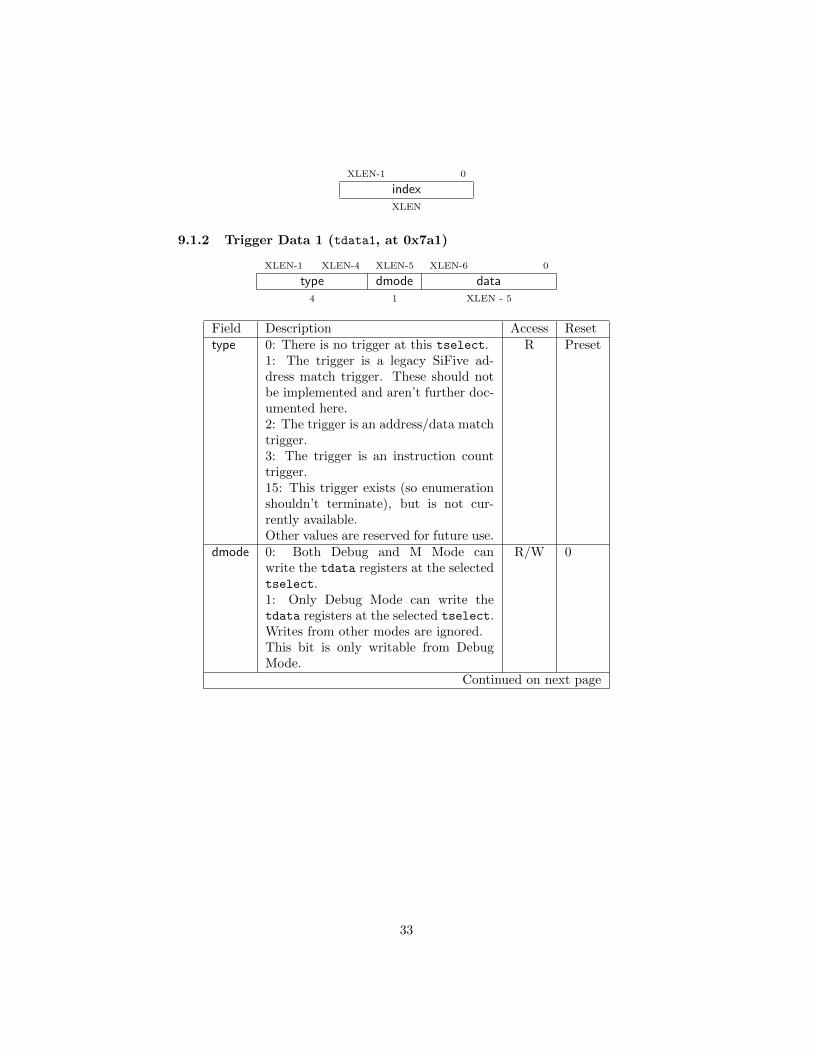
9.1.2 Trigger Data 1 (tdata1, at 0x7a1)
XLEN-1 XLEN-4 XLEN-5 XLEN-6 0
type dmode data4 1 XLEN - 5
Field Description Access Resettype 0: There is no trigger at this tselect.
1: The trigger is a legacy SiFive ad-dress match trigger. These should notbe implemented and aren’t further doc-umented here.2: The trigger is an address/data matchtrigger.3: The trigger is an instruction counttrigger.15: This trigger exists (so enumerationshouldn’t terminate), but is not cur-rently available.Other values are reserved for future use.
R Preset
dmode 0: Both Debug and M Mode canwrite the tdata registers at the selectedtselect.1: Only Debug Mode can write thetdata registers at the selected tselect.Writes from other modes are ignored.This bit is only writable from DebugMode.
R/W 0
Continued on next page
33

data Trigger-specific data. R/W Preset
9.1.3 Trigger Data 2 (tdata2, at 0x7a2)
Trigger-specific data.
XLEN-1 0
dataXLEN
9.1.4 Trigger Data 3 (tdata3, at 0x7a3)
Trigger-specific data.
XLEN-1 0
dataXLEN
9.1.5 Match Control (mcontrol, at 0x7a1)
This register is accessible as tdata1 when type is 2.Writing unsupported values to any field in this register results in the reset
value being written instead. When a debugger wants to use a feature, it mustwrite the appropriate value and then read back the register to determine whetherit is supported.
Address and data trigger implementation are heavily dependent on how theprocessor core is implemented. To accommodate various implementations, loadand store address and data triggers may fire at whatever point in time is mostconvenient for the implementation. Following the suggestions in the definitionsof store and load will lead to the best user experience, however.
XLEN-1 XLEN-4 XLEN-5 XLEN-6 XLEN-11 XLEN-12 20 19 18
type dmode maskmax 0 select timing4 1 6 XLEN - 31 1 1
17 12 11 10 7 6 5 4
action chain match m h s6 1 4 1 1 1
3 2 1 0
u execute store load1 1 1 1
34
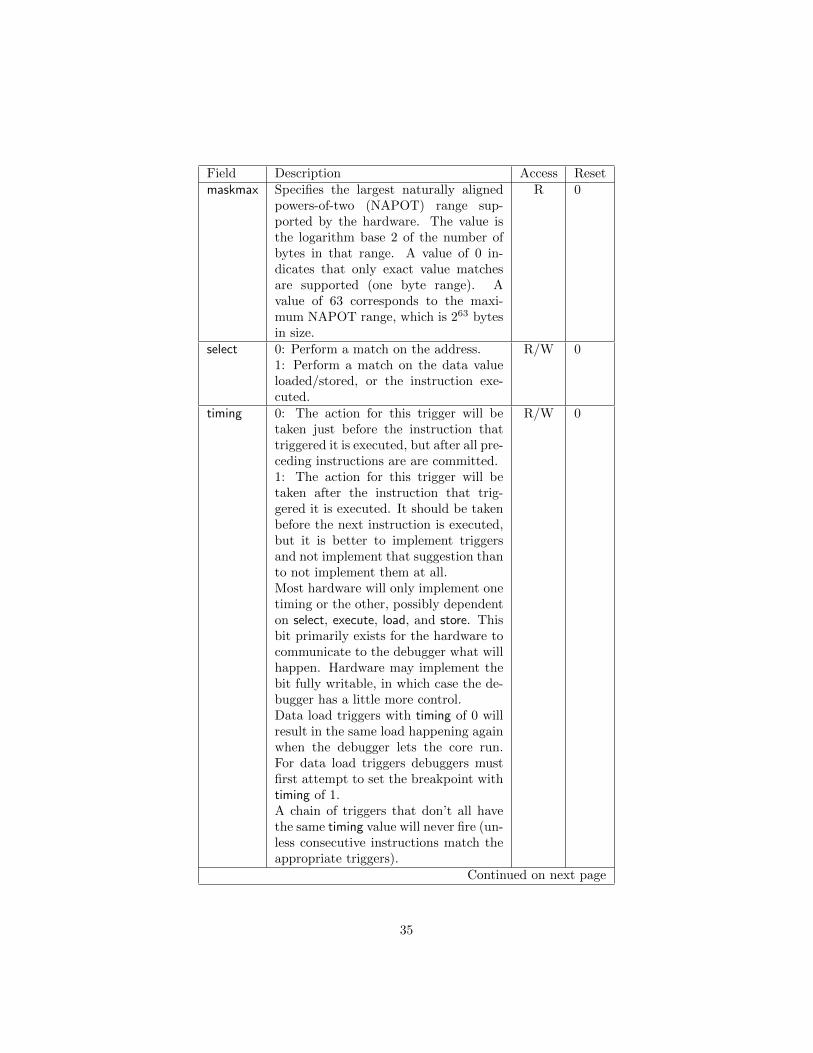
Field Description Access Resetmaskmax Specifies the largest naturally aligned
powers-of-two (NAPOT) range sup-ported by the hardware. The value isthe logarithm base 2 of the number ofbytes in that range. A value of 0 in-dicates that only exact value matchesare supported (one byte range). Avalue of 63 corresponds to the maxi-mum NAPOT range, which is 263 bytesin size.
R 0
select 0: Perform a match on the address.1: Perform a match on the data valueloaded/stored, or the instruction exe-cuted.
R/W 0
timing 0: The action for this trigger will betaken just before the instruction thattriggered it is executed, but after all pre-ceding instructions are are committed.1: The action for this trigger will betaken after the instruction that trig-gered it is executed. It should be takenbefore the next instruction is executed,but it is better to implement triggersand not implement that suggestion thanto not implement them at all.Most hardware will only implement onetiming or the other, possibly dependenton select, execute, load, and store. Thisbit primarily exists for the hardware tocommunicate to the debugger what willhappen. Hardware may implement thebit fully writable, in which case the de-bugger has a little more control.Data load triggers with timing of 0 willresult in the same load happening againwhen the debugger lets the core run.For data load triggers debuggers mustfirst attempt to set the breakpoint withtiming of 1.A chain of triggers that don’t all havethe same timing value will never fire (un-less consecutive instructions match theappropriate triggers).
R/W 0
Continued on next page
35

action Determines what happens when thistrigger matches.0: Raise a debug exception. (Used whensoftware wants to use the trigger modulewithout an external debugger attached.)1: Enter Debug Mode. (Only supportedwhen dmode is 1.)2: Start tracing.3: Stop tracing.4: Emit trace data for this match. If itis a data access match, emit appropriateLoad/Store Address/Data. If it is aninstruction execution, emit its PC.Other values are reserved for future use.
R/W 0
chain 0: When this trigger matches, the con-figured action is taken.1: While this trigger does not match, itprevents the trigger with the next indexfrom matching.
R/W 0
match 0: Matches when the value equalstdata2.1: Matches when the top M bits ofthe value match the top M bits oftdata2. M is XLEN-1 minus the indexof the least-significant bit containing 0in tdata2.2: Matches when the value is greaterthan or equal to tdata2.3: Matches when the value is less thantdata2.4: Matches when the lower half of thevalue equals the lower half of tdata2 af-ter the lower half of the value is ANDedwith the upper half of tdata2.5: Matches when the upper half of thevalue equals the lower half of tdata2 af-ter the upper half of the value is ANDedwith the upper half of tdata2.Other values are reserved for future use.
R/W 0
Continued on next page
36

m When set, enable this trigger in Mmode.
R/W 0
h When set, enable this trigger in H mode. R/W 0s When set, enable this trigger in S mode. R/W 0u When set, enable this trigger in U mode. R/W 0execute When set, the trigger fires on the ad-
dress or opcode of an instruction that isexecuted.
R/W 0
store When set, the trigger fires on the ad-dress or data of a store.
R/W 0
load When set, the trigger fires on the ad-dress or data of a load.
R/W 0
9.1.6 Instruction Count (icount, at 0x7a1)
This register is accessible as tdata1 when type is 3.Warning! icount is just a proposal. So far nobody has commented
on it, so it could very easily be removed or changed in the future.Writing unsupported values to any field in this register results in the reset
value being written instead. When a debugger wants to use a feature, it mustwrite the appropriate value and then read back the register to determine whetherit is supported.
This trigger type is intended to be used as a single step that’s usefulboth for external debuggers and for software monitor programs. As suchit is not necessary to support count greater than 1. The only two combi-nations of the mode bits that are useful in those scenarios are u by itself,or m, h, s, and u all set.
If the hardware limits count to 1, and changes mode bits instead ofdecrementing count, this register can be implemented with just 2 bits. Onefor u, and one for m, h, and s tied together. If only the external debuggeror only a software monitor needs to be supported, a single bit is enough.
XLEN-1 XLEN-4 XLEN-5 XLEN-6 24 23 10 9
type dmode 0 count m4 1 XLEN - 29 14 1
8 7 6 5 0
h s u action1 1 1 6
37

Field Description Access Resetcount When count is decremented to 0, the
trigger fires. Instead of changing countfrom 1 to 0, it is also acceptable forhardware to clear m, h, s, and u. Thisallows count to be hard-wired to 1 if thisregister just exists for single step.
R/W 1
m When set, every instruction completedin M mode decrements count by 1.
R/W 0
h When set, every instruction completedin H mode decrements count by 1.
R/W 0
s When set, every instruction completedin S mode decrements count by 1.
R/W 0
u When set, every instruction completedin U mode decrements count by 1.
R/W 0
action Determines what happens when thistrigger matches.0: Raise a debug exception. (Used whensoftware wants to use the trigger modulewithout an external debugger attached.)1: Enter Debug Mode. (Only supportedwhen dmode is 1.)2: Start tracing.3: Stop tracing.4: Emit trace data for this match. If itis a data access match, emit appropriateLoad/Store Address/Data. If it is aninstruction execution, emit its PC.Other values are reserved for future use.
R/W 0
10 JTAG Debug Transport Module
This Debug Transport Module is based around a normal JTAG Test AccessPort (TAP). The JTAG TAP allows access to arbitrary JTAG registers by firstselecting one using the JTAG instruction register (IR), and then accessing itthrough the JTAG data register (DR).
10.1 Background
JTAG refers to IEEE Std 1149.1-2013. It is a standard that defines test logicthat can be included in an integrated circuit to test the interconnections betweenintegrated circuits, test the integrated circuit itself, and observe or modify circuitactivity during the components normal operation. We’re using it for the thirdcase here. The standard defines a Test Access Port (TAP) that can be used toread and write a few custom registers, which can be used to communicate with
38

debug hardware in a component.
10.2 JTAG Connector
Every target’s JTAG connector seems to have its own pinout. To make it easy toacquire debug hardware, this spec recommends a connector that is compatiblewith the Cortex Debug Connector, as described below.
The connector is a .05”-spaced, gold-plated male header with .016” thickhardened copper or beryllium bronze square posts (SAMTEC FTSH-105 orequivalent). Female connectors are compatible 20 µm gold connectors in orderto prevent oxide build-up on tin connectors.
Viewing the male header from above (the pins pointing at your eye), atarget’s connector looks as it does in Table 10. The function of each pin isdescribed in Table 11.
Table 10: JTAG Connector DiagramVCC 1 2 TMSGND 3 4 TCKGND 5 6 TDOKEY 7 8 TDIN/C 9 10 RESET
Target connectors may be shrouded. In that case the key slot should be nextto pin 5. Female headers should have a matching key.
Debug adapters should be tagged or marked with their isolation voltagethreshold (i.e. unisolated, 250V, etc.).
All debug adapter pins other than GND should be current-limited to 20mA.
10.3 JTAG Registers
JTAG DTMs should use a 5-bit JTAG IR. When the TAP is reset, IR mustdefault to 00001, selecting the IDCODE instruction. A full list of JTAG regis-ters along with their encoding is in Table 12. The only regular JTAG registersa debugger might use are BYPASS and IDCODE, but the JTAG standard rec-ommends a lot of other instructions so we leave IR space for them. If they arenot implemented, then they must select the BYPASS register.
10.3.1 IDCODE (00001)
This register is selected (in IR) when the TAP state machine is reset. Itsdefinition is exactly as defined in IEEE Std 1149.1-2013.
31 28 27 12 11 1 0
Version PartNumber ManufId 14 16 11 1
39

Table 11: JTAG Connector Pinout1 VCC Power provided by the target, which may be used to
power the debug adapter. Must be able to source at least25mA. This signal also serves as the reference voltage forlogic high.This pin must be clearly marked in both male and femaleheaders.
2 TMS JTAG TMS signal, driven by debug adapter.3 GND Target ground.4 TCK JTAG TCK signal, driven by the debug adapter.5 GND Target ground.6 TDO JTAG TDO signal, driven by the target.7 KEY This pin should be clipped in male connectors, and
plugged in female connectors. Electrically it must not beconnected.
8 TDI JTAG TDI signal, driven by the debug adapter.This pin may be used by a target to sense a debugger atreset by weakly pulling this signal high during a briefdetection period at reset. Debuggers should drive TDI lowwhen the interface is idle.
9 N/C Not connected in either target or debug adapter. May beused in future specs.
10 RESET Reset signal, driven by the debug adapter. This may beactive low or active high, depending on the target’srequirements. A debug adapter must accommodate eitheroption. Asserting reset should reset any RISC-V cores aswell as any other peripherals on the PCB. If notimplemented in a target, this pin must not be connected.
40

Table 12: JTAG TAP RegistersAddress Name Description
00000 BYPASS JTAG recommends this encoding00001 IDCODE JTAG recommends this encoding00010 SAMPLE JTAG requires this instruction00011 PRELOAD JTAG requires this instruction00100 EXTEST JTAG requires this instruction00101 CLAMP JTAG recommends this instruction00110 CLAMP HOLD JTAG recommends this instruction00111 CLAMP RELEASE JTAG recommends this instruction01000 HIGHZ JTAG recommends this instruction01001 IC RESET JTAG recommends this instruction01010 TMP STATUS JTAG recommends this instruction01011 INIT SETUP JTAG recommends this instruction01100 INIT SETUP CLAMP JTAG recommends this instruction01101 INIT RUN JTAG recommends this instruction01110 Unused (BYPASS) Reserved for future JTAG01111 Unused (BYPASS) Reserved for future JTAG10000 DTM Control For Debugging10001 Debug Bus Access For Debugging10010 Reserved (BYPASS) Reserved for future RISC-V debugging10011 Reserved (BYPASS) Reserved for future RISC-V debugging10100 Reserved (BYPASS) Reserved for future RISC-V debugging10101 Reserved (BYPASS) Reserved for future RISC-V standards10110 Reserved (BYPASS) Reserved for future RISC-V standards10111 Reserved (BYPASS) Reserved for future RISC-V standards11000 Unused (BYPASS) Reserved for customization11001 Unused (BYPASS) Reserved for customization11010 Unused (BYPASS) Reserved for customization11011 Unused (BYPASS) Reserved for customization11100 Unused (BYPASS) Reserved for customization11101 Unused (BYPASS) Reserved for customization11110 Unused (BYPASS) Reserved for customization11111 BYPASS JTAG requires this encoding
41

Field Description Access ResetVersion Identifies the release version of this part. R PresetPartNumber Identifies the designer’s part number of
this part.R Preset
ManufId Identifies the designer/manufacturer ofthis part. Bits 6:0 must be bits 6:0 ofthe designer/manufacturer’s Identifica-tion Code as assigned by JEDEC Stan-dard JEP106. Bits 10:7 contain themodulo-16 count of the number of con-tinuation characters (0x7f) in that sameIdentification Code.
R Preset
10.3.2 DTM Control (dtmcontrol, at 10000)
The size of this register will remain constant in future versions so that a debuggercan always determine the version of the DTM.
31 17 16 15 14 13
0 dbusreset 0 hiabits15 1 1 2
12 10 9 8 7 4 3 0
idle dbusstat loabits version3 2 4 4
Field Description Access Resetdbusreset Writing 1 to this bit resets the dbus con-
troller, clearing any sticky error state.W1 0
hiabits Bits 5:4 of abits, which describes the sizeof address in dbus.
R Preset
idle The number of cycles a debuggerneeds to send the target through Run-Test/Idle after every dbus scan.0: It’s not necessary to enter Run-Test/Idle at all.1: Enter Run-Test/Idle and leave it im-mediately.2: Enter Run-Test/Idle and stay therefor 1 cycle before leaving.And so on.
R Preset
Continued on next page
42
dbusstat 0: No error.2: An operation failed.3: An operation was attempted while abus access was still in progress.
R 0
loabits Bits 3:0 of abits, which describes the sizeof address in dbus.
R Preset
version 0 indicates the version described in thisdocument. Other values are reserved forfuture use.
R 0
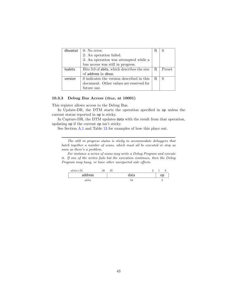
10.3.3 Debug Bus Access (dbus, at 10001)
This register allows access to the Debug Bus.In Update-DR, the DTM starts the operation specified in op unless the
current status reported in op is sticky.In Capture-DR, the DTM updates data with the result from that operation,
updating op if the current op isn’t sticky.See Section A.1 and Table 13 for examples of how this plays out.
The still in progress status is sticky to accommodate debuggers thatbatch together a number of scans, which must all be executed or stop assoon as there’s a problem.
For instance a series of scans may write a Debug Program and executeit. If one of the writes fails but the execution continues, then the DebugProgram may hang, or have other unexpected side effects.
abits+35 36 35 2 1 0
address data opabits 34 2
43
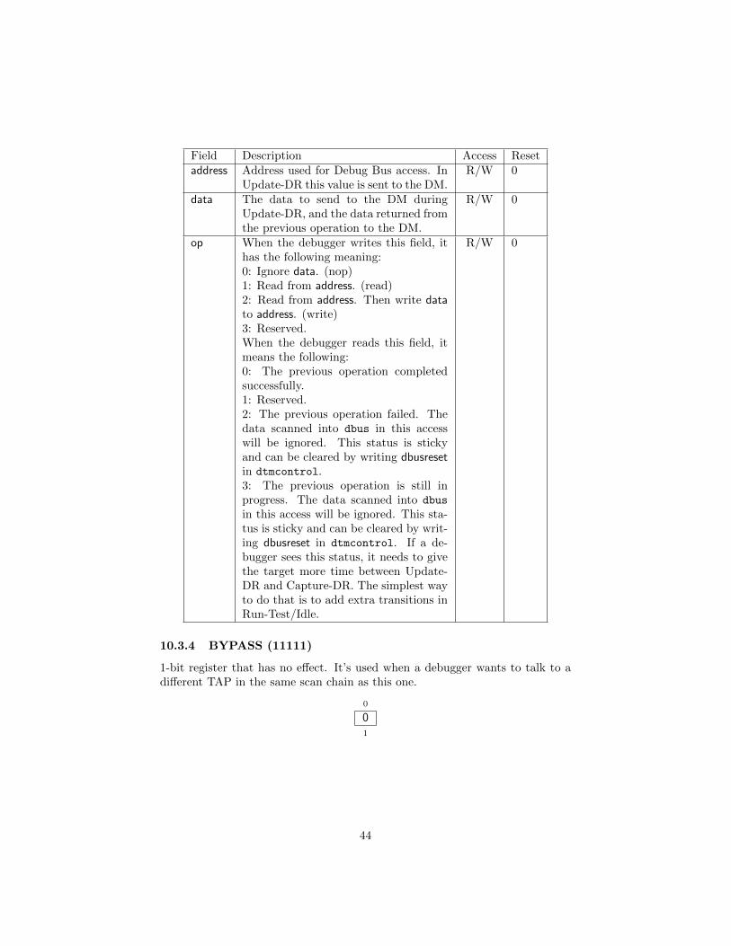
Field Description Access Resetaddress Address used for Debug Bus access. In
Update-DR this value is sent to the DM.R/W 0
data The data to send to the DM duringUpdate-DR, and the data returned fromthe previous operation to the DM.
R/W 0
op When the debugger writes this field, ithas the following meaning:0: Ignore data. (nop)1: Read from address. (read)2: Read from address. Then write datato address. (write)3: Reserved.When the debugger reads this field, itmeans the following:0: The previous operation completedsuccessfully.1: Reserved.2: The previous operation failed. Thedata scanned into dbus in this accesswill be ignored. This status is stickyand can be cleared by writing dbusresetin dtmcontrol.3: The previous operation is still inprogress. The data scanned into dbus
in this access will be ignored. This sta-tus is sticky and can be cleared by writ-ing dbusreset in dtmcontrol. If a de-bugger sees this status, it needs to givethe target more time between Update-DR and Capture-DR. The simplest wayto do that is to add extra transitions inRun-Test/Idle.
R/W 0
10.3.4 BYPASS (11111)
1-bit register that has no effect. It’s used when a debugger wants to talk to adifferent TAP in the same scan chain as this one.
0
01
44

A Debugger Implementation
This section details how an external debugger might use the described debuginterface to perform some common operations on RISC-V cores using the JTAGDTM. All these examples assume a 32-bit core but it should be easy to adaptthe examples to 64- or 128-bit cores.
A.1 Debug Bus Access
To read an arbitrary Debug Bus register, select dbus, and scan in a value withop set to 1, and address set to the desired register address. In Update-DRthe operation will start, and in Capture-DR its results will be captured intodata. If the operation didn’t complete in time, op will be 3 and the value indata must be ignored. The error condition must be cleared by writing dbusresetin dtmcontrol, and then the operation must be tried again. This time thedebugger should allow for more time between Capture-DR and Update-DR.
To write an arbitrary Debug Bus register, select dbus, and scan in a valuewith op set to 2, and address and data set to the desired register address anddata respectively. From then on everything happens exactly as with a read,except that a write is also performed right after the read. The operation isn’tconsidered complete until the write has happened.
It should almost never be necessary to scan IR, avoiding a big part of theinefficiency in typical JTAG use.
A.2 Debug RAM
All operations are executed by writing a debug program to Debug RAM, andhaving the core execute it. This comes down to a series of Debug Bus accessesas described above.
First, select the hart of interest by writing its ID to hartid in dmcontrol.Then write the program to Debug RAM with a series of writes to 0x0 – 0xf. Onthe last write, set the interrupt bit. This triggers program execution. Performa read to poll the interrupt bit to wait for it to clear. Typically JTAG will beso slow that the interrupt bit will be clear on the very next scan. An efficientdebugger can optimistically assume all operations will complete immediately. Ifit discovers that is not the case (by seeing interrupt is still set on a scan) it canadapt by increasing the delay between scans.
That means if eg. you are doing a block write and have the program mostlyset up, you can write a new data value and set the interrupt bit every timethrough the loop using a write operation.
A.3 Main Loop
A debugger continuously monitors haltsum to see if any harts have sponta-neously halted. While this is going on, a debugger might perform a quick
45
operation (most likely a memory access) by writing a debug program that endswith a jump to resume, and asserting a hart’s Debug Interrupt.
To halt a hart, the debugger writes a debug program that sets halt and endswith a jump to resume. Then it asserts the hart’s Debug Interrupt.
Once halted, the debugger can write debug programs in exactly the sameway that it can when the hart is running. The only difference is that in this casethe jump to resume ends in up in Debug ROM code that waits until the debuginterrupt is set again, instead of by continuing normal execution. To resumenormal execution, the debugger writes a debug program that clears halt beforejumping to resume.
Performing operations then all comes down to writing the appropriate pro-gram to Debug RAM, so the sections below mostly consist of short programlistings. The Debug ROM already takes care of saving s0 and s1 so thoseregisters can be used without any extra precautions.
A.4 Reading Memory
Execute the following program, and then read the value that was read fromdata.
lw s1, address
lw s0, 0(s1)
sw s0, data
j resume
address:.word ADDRESS
data: .word DATA
A shorter program is possible by hardcoding the address in a set of lui/lwinstructions, but this technique would be limited to 32-bit cores. This versionalso has the nice property that to immediately read from a different address,only 1 word in Debug RAM needs to be changed.
A slightly different program can be used to read memory very efficiently:
lw s1, data
lw s0, 0(s1)
sw s0, data
j resume
data: .word ADDRESS
In this case data is used both for the address and data. After this programis executed, the data value is in data. Since a JTAG bus write first performs aread, a single scan can read this data value, write the next address value, andassert the Debug Interrupt. As many of those scans can be used as necessary,and every scan results in 32 bits of data being read. The debugger does need tomake sure interrupt is clear in each read. If it is not the data cannot be trusted,and the same address should be read again.
46
Table 13 shows the scans involved in reading a single word using this method.In this table dram[n] refers to the location in Debug RAM with address n. Ifmore words need to be read, then this can by pipelined, by changing the scanin step 6 to a write of the next address.
A.5 Writing Memory
To write a single word:
lw s1, data
lw s0, address
sw s1, 0(s0)
j resume
address:.word ADDRESS
data: .word DATA
To efficiently write a block of memory, the debug program can take care ofincrementing the address. First save t0 and load the start address into it:
sw t0, data
lw t0, address
j resume
address:.word ADDRESS
data: .word 0
Then write the following program with the first data value, and assert theDebug Interrupt. Additional words can be written by writing the next datavalue and asserting the Debug Interrupt.
lw s0, data
sw s0, 0(t0)
addi t0, t0, 4
j resume
data: .word DATA
After the second program is written, each word can be written to thetarget in 43 TCK cycles. That’s 75% efficient, and translates to a down-load speed of 908KB/s at a 10MHz TCK. That should be good enough thatit’s not worth making the JTAG interface more complex to improve theefficiency. (This assumes the Debug Bus uses 5 address bits and that thedebugger never has to wait for the core.)
A.6 Halt
To halt a hart, first write the code to be executed to Debug RAM. Then assertthe relevant Debug Interrupt.
The code to be executed must set halt. Reading pc and dcsr is optional,but it’s extremely common for a debugger to do this immediately after halting.
47
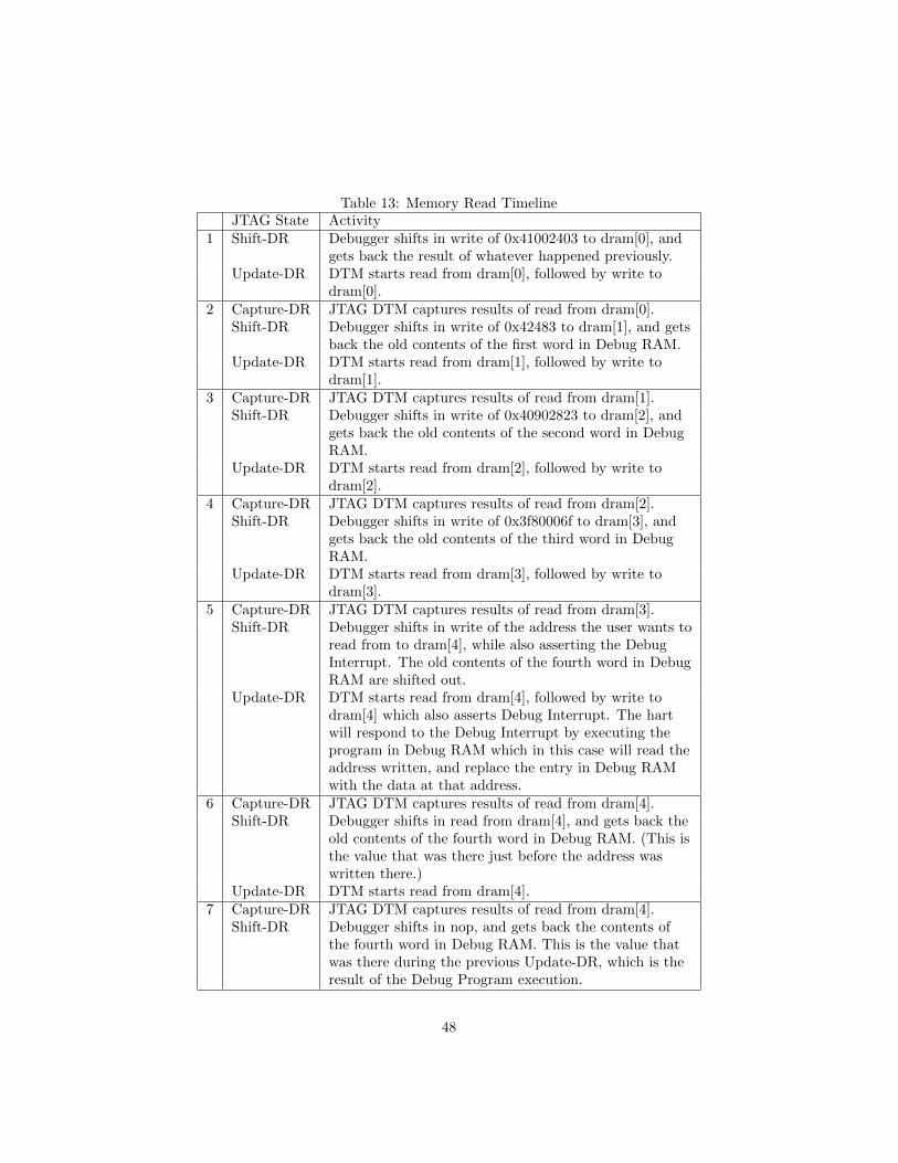
Table 13: Memory Read TimelineJTAG State Activity
1 Shift-DR Debugger shifts in write of 0x41002403 to dram[0], andgets back the result of whatever happened previously.
Update-DR DTM starts read from dram[0], followed by write todram[0].
2 Capture-DR JTAG DTM captures results of read from dram[0].Shift-DR Debugger shifts in write of 0x42483 to dram[1], and gets
back the old contents of the first word in Debug RAM.Update-DR DTM starts read from dram[1], followed by write to
dram[1].3 Capture-DR JTAG DTM captures results of read from dram[1].
Shift-DR Debugger shifts in write of 0x40902823 to dram[2], andgets back the old contents of the second word in DebugRAM.
Update-DR DTM starts read from dram[2], followed by write todram[2].
4 Capture-DR JTAG DTM captures results of read from dram[2].Shift-DR Debugger shifts in write of 0x3f80006f to dram[3], and
gets back the old contents of the third word in DebugRAM.
Update-DR DTM starts read from dram[3], followed by write todram[3].
5 Capture-DR JTAG DTM captures results of read from dram[3].Shift-DR Debugger shifts in write of the address the user wants to
read from to dram[4], while also asserting the DebugInterrupt. The old contents of the fourth word in DebugRAM are shifted out.
Update-DR DTM starts read from dram[4], followed by write todram[4] which also asserts Debug Interrupt. The hartwill respond to the Debug Interrupt by executing theprogram in Debug RAM which in this case will read theaddress written, and replace the entry in Debug RAMwith the data at that address.
6 Capture-DR JTAG DTM captures results of read from dram[4].Shift-DR Debugger shifts in read from dram[4], and gets back the
old contents of the fourth word in Debug RAM. (This isthe value that was there just before the address waswritten there.)
Update-DR DTM starts read from dram[4].7 Capture-DR JTAG DTM captures results of read from dram[4].
Shift-DR Debugger shifts in nop, and gets back the contents ofthe fourth word in Debug RAM. This is the value thatwas there during the previous Update-DR, which is theresult of the Debug Program execution.
48

dpc: csrsi DCSR, DCSR_HALT_MASK
dcsr: csrr s1, DPC
sw s1, dpc
csrr s1, DCSR
sw s1, dcsr
j resume
A.7 Reading Registers
Eg. how to read f1:
fsw f1, data
j resume
data: .word 0
A.8 Writing Registers
Eg. how to write mepc.
lw s0, data
csrw MEPC, s0
j resume
data: .word DATA
A.9 Running
To let the core run once it’s halted, the debugger needs to first clear the HaltNotification using the debug bus directly. If the debugger used any registersbesides s0 and s1 as scratch registers, now is the time to restore them. Fi-nally:
csrci DCSR, DCSR_HALT_MASK
j resume
A.10 Single Step
A debugger can single step the core by setting a breakpoint on the next instruc-tion and letting the core run, or by asking the hardware to perform a singlestep. The former requires the debugger to have much more knowledge of thehardware than the latter, so the latter is preferred.
Using the hardware single step feature is almost the same as regular running.The debugger just sets step in dcsr before leaving Debug Mode. The corebehaves exactly as in the running case, except that interrupts are left off and itonly fetches and executes a single instruction before re-entering Debug Mode.
49
A.11 Handling Exceptions
Generally the debugger can avoid exceptions by being careful with the programsit writes. Sometimes they are unavoidable though, eg. if the user asks to accessmemory or a CSR that is not implemented. A typical debugger will not knowenough about the platform to return an error, and must attempt the access todetermine the outcome.
When an exception occurs in Debug Mode no registers are updated, butDebug ROM will write 0xffffffff to the last word of Debug RAM. If the debuggerthinks an exception may have occurred it should check for that. If no exceptionoccurred in the last entry to Debug RAM, then the word must contain 0. Ifthere was an exception, it’s left to the debugger to know what must have causedit.
B Debug ROM Source
#include "riscv/encoding.h"
#define DEBUG_RAM 0x400
#define DEBUG_RAM_SIZE 64
#define CLEARDEBINT 0x100
#define SETHALTNOT 0x10c
.global entry
.global resume
.global exception
# Automatically called when Debug Mode is first entered.
entry: j _entry
# Should be called by Debug RAM code that has finished execution and
# wants to return to Debug Mode.
resume:
j _resume
exception:
# Set the last word of Debug RAM to all ones, to indicate that we hit
# an exception.
li s0, ~0
j _resume2
_resume:
li s0, 0
_resume2:
fence
50

# Restore s1.
csrr s1, CSR_MISA
bltz s1, restore_not_32
restore_32:
lw s1, (DEBUG_RAM + DEBUG_RAM_SIZE - 4)(zero)
j finish_restore
restore_not_32:
slli s1, s1, 1
bltz s1, restore_128
restore_64:
ld s1, (DEBUG_RAM + DEBUG_RAM_SIZE - 8)(zero)
j finish_restore
restore_128:
nop #lq s1, (DEBUG_RAM + DEBUG_RAM_SIZE - 16)(zero)
finish_restore:
# s0 contains ~0 if we got here through an exception, and 0 otherwise.
# Store this to the last word in Debug RAM so the debugger can tell if
# an exception occurred.
sw s0, (DEBUG_RAM + DEBUG_RAM_SIZE - 4)(zero)
# Clear debug interrupt.
csrr s0, CSR_MHARTID
sw s0, CLEARDEBINT(zero)
check_halt:
csrr s0, CSR_DCSR
andi s0, s0, DCSR_HALT
beqz s0, exit
j wait_for_interrupt
exit:
# Restore s0.
csrr s0, CSR_DSCRATCH
dret
_entry:
# Save s0 in DSCRATCH
csrw CSR_DSCRATCH, s0
# Check why we’re here
csrr s0, CSR_DCSR
# cause is in bits 8:6 of dcsr
andi s0, s0, DCSR_CAUSE
addi s0, s0, -(DCSR_CAUSE_DEBUGINT<<6)
bnez s0, spontaneous_halt
51

jdebugram:
# Save s1 so that the debug program can use two registers.
fence.i
csrr s0, CSR_MISA
bltz s0, save_not_32
save_32:
sw s1, (DEBUG_RAM + DEBUG_RAM_SIZE - 4)(zero)
jr zero, DEBUG_RAM
save_not_32:
slli s0, s0, 1
bltz s0, save_128
save_64:
sd s1, (DEBUG_RAM + DEBUG_RAM_SIZE - 8)(zero)
jr zero, DEBUG_RAM
save_128:
nop #sq s1, (DEBUG_RAM + DEBUG_RAM_SIZE - 16)(zero)
jr zero, DEBUG_RAM
spontaneous_halt:
csrr s0, CSR_MHARTID
sw s0, SETHALTNOT(zero)
csrsi CSR_DCSR, DCSR_HALT
wait_for_interrupt:
csrr s0, CSR_DCSR
andi s0, s0, DCSR_DEBUGINT
beqz s0, wait_for_interrupt
j jdebugram
C Trace Module
This part of the spec needs work before it’s ready to be implemented,which is why it’s in the appendix. It’s left here to give a rough ideaof some of the issues to consider.
Aside from viewing the current state of a core, knowing what happened inthe past can be incredibly helpful. Capturing an execution trace can give a userthat view. Unfortunately processors run so fast that they generate trace dataat a very large rate. To help deal with this, the trace data format allows forsome simple compression.
The trace functionality described here aims to support 3 different use cases:
1. Full reconstruction of all processor state, including register values etc.To achieve this goal the decoder will have to know what code is beingexecuted, and know the exact behavior of every RISC-V instruction.
52

2. Reconstruct just the instruction stream. Get enough data from the tracestream that it is possible to make a list of every instruction executed. Thisis possible without knowing anything about the code or the core executingit.
3. Watch memory accesses for a certain memory region.
Trace data may be stored to a special on-core RAM, RAM on the systembus, or to a dedicated off-chip interface. Only the system RAM destination iscovered here.
C.1 Trace Data Format
Trace data should be both compact and easy to generate. Ideally it’s also easyto decode, but since decoding doesn’t have to happen in real time and willusually have a powerful workstation to do the work, this is the least importantconcern.
Trace data consists of a stream of 4-bit packets, which are stored in memoryin 32-bit words by putting the first packet in bits 3:0 of the 32-bit word, thesecond packet into bits 7:4, and so on. Trace packets and their encoding arelisted in Table 14.
Several header packets are followed by a Value Sequence, which can encodevalues between 4 and 64 bits. The sequence consists first of a 4-bit size packetwhich contains a single number N. It is followed by N+1 4-bit packets whichcontain the value. The first packet contains bits 3:0 of the value. The nextpacket contains bits 7:4, and so on.
C.2 Trace Events
Trace events are events that occur when a core is running that result in tracepackets being emitted. They are listed in Table 15.
C.3 Synchronization
If a trace buffer wraps, it is no longer clear what in the buffer is a headerand what isn’t. To guarantee that a trace decoder can sync up easily, eachtrace buffer must have 8 synchronization points, spaced evenly throughout thebuffer, with the first one at the very start of the buffer. A synchronization pointis simply an address where there is guaranteed to be a sequence header. Tomake this happen, the trace source can insert a number of Nop headers into thesequence just before writing to the synchronization point.
Aside from synchronizing a place in the data stream, it’s also necessary tosend a full PC, Read Address, Write Address, and Timestamp in order for thoseto be fully decoded. Ideally that happens the first time after every synchroniza-tion point, but bandwidth might prevent that. A trace source should attemptto send one full value for each of these (assuming they’re enabled) soon aftereach synchronization point.
53
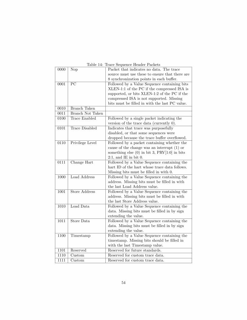
Table 14: Trace Sequence Header Packets0000 Nop Packet that indicates no data. The trace
source must use these to ensure that there are8 synchronization points in each buffer.
0001 PC Followed by a Value Sequence containing bitsXLEN-1:1 of the PC if the compressed ISA issupported, or bits XLEN-1:2 of the PC if thecompressed ISA is not supported. Missingbits must be filled in with the last PC value.
0010 Branch Taken0011 Branch Not Taken0100 Trace Enabled Followed by a single packet indicating the
version of the trace data (currently 0).0101 Trace Disabled Indicates that trace was purposefully
disabled, or that some sequences weredropped because the trace buffer overflowed.
0110 Privilege Level Followed by a packet containing whether thecause of the change was an interrupt (1) orsomething else (0) in bit 3, PRV[1:0] in bits2:1, and IE in bit 0.
0111 Change Hart Followed by a Value Sequence containing thehart ID of the hart whose trace data follows.Missing bits must be filled in with 0.
1000 Load Address Followed by a Value Sequence containing theaddress. Missing bits must be filled in withthe last Load Address value.
1001 Store Address Followed by a Value Sequence containing theaddress. Missing bits must be filled in withthe last Store Address value.
1010 Load Data Followed by a Value Sequence containing thedata. Missing bits must be filled in by signextending the value.
1011 Store Data Followed by a Value Sequence containing thedata. Missing bits must be filled in by signextending the value.
1100 Timestamp Followed by a Value Sequence containing thetimestamp. Missing bits should be filled inwith the last Timestamp value.
1101 Reserved Reserved for future standards.1110 Custom Reserved for custom trace data.1111 Custom Reserved for custom trace data.
54

Table 15: Trace Data EventsOpcode Actionjal If emitbranch is disabled but emitpc is enabled, emit 2
PC values: first the address of the instruction, then theaddress being jumped to.
jalr If emitbranch is disabled but emitpc is enabled, emit 2PC values: first the address of the instruction, then theaddress being jumped to. Otherwise, if emitstoredata isenabled emit just the destination PC.
BRANCH If emitbranch is enabled, emit either Branch Taken orBranch Not Taken. Otherwise if emitpc is enabled andthe branch is taken, emit 2 PC values: first the addressof the branch, then the address being branched to.
LOAD If emitloadaddr is enabled, emit the address. Ifemitloaddata is enabled, emit the data that was loaded.
STORE If emitstoreaddr is enabled, emit the address. Ifemitstoredata is enabled, emit the data that is stored.
Traps scall, sbreak, ecall, ebreak, and eret emit the sameas if they were jal instructions. In addition they alsoemit a Privilege Level sequence.
Interrupts Emit PC (if enabled) of the last instruction executed.Emit Privilege Level (if enabled). Finally emit the newPC (if enabled).
CSR instructions For reads emit Load Data (if enabled). For writes emitStore Data (if enabled).
Data Dropped After packet sequences are dropped because data isgenerated too quickly, Trace Disabled must be emitted.It’s not necessary to follow that up with a TraceEnabled sequence.
55

C.4 Trace Registers
Table 16: Trace RegistersAddress Name
0x728 Trace0x729 Trace Buffer Start0x72a Trace Buffer End0x72b Trace Buffer Write
C.4.1 Trace (trace, at 0x728)
31 25 24 23 22 21 20
0 wrapped emittimestamp emitstoredata emitloaddata emitstoreaddr7 1 1 1 1 1
19 18 17 16 15 10 9 8
emitloadaddr emitpriv emitbranch emitpc 0 fullaction1 1 1 1 6 2
7 6 5 4 3 2 1 0
0 destination 0 stall discard supported2 2 1 1 1 1
56

Field Description Access Resetwrapped 1 if the trace buffer has wrapped since
the last time discard was written. 0 oth-erwise.
R 0
emittimestamp Emit Timestamp trace sequences. R/W 0emitstoredata Emit Store Data trace sequences. R/W 0emitloaddata Emit Load Data trace sequences. R/W 0emitstoreaddr Emit Store Address trace sequences. R/W 0emitloadaddr Emit Load Address trace sequences. R/W 0emitpriv Emit Privilege Level trace sequences. R/W 0emitbranch Emit Branch Taken and Branch Not
Taken trace sequences.R/W 0
emitpc Emit PC trace sequences. R/W 0fullaction Determine what happens when the trace
buffer is full. 0 means wrap and over-write. 1 means turn off trace untildiscard is written as 1. 2 means causea trace full exception. 3 is reserved forfuture use.
R/W 0
destination 0: Trace to a dedicated on-core RAM(which is not further defined in thisspec).1: Trace to RAM on the system bus.2: Send trace data to a dedicated off-chip interface (which is not defined inthis spec). This does not affect execu-tion speed.3: Reserved for future use.Options 0 and 1 slow down execution(eg. because of system bus contention).
R/W Preset
Continued on next page
57
stall When 1, the trace logic may stall pro-cessor execution to ensure it can emitall the trace sequences required. When0 individual trace sequences may bedropped.
R/W 1
discard Writing 1 to this bit tells the trace logicthat any trace collected is no longer re-quired. When tracing to RAM, it resetsthe trace write pointer to the start ofthe memory, as well as wrapped.
W1 0
C.4.2 Trace Buffer Start (tbufstart, at 0x729)
If destination is 1, this register contains the start address of block of RAMreserved for trace data.
XLEN-1 0
addressXLEN
C.4.3 Trace Buffer End (tbufend, at 0x72a)
If destination is 1, this register contains the end address (exclusive) of block ofRAM reserved for trace data.
XLEN-1 0
addressXLEN
C.4.4 Trace Buffer Write (tbufwrite, at 0x72b)
If destination is 1, this read-only register contains the address that the next tracepacket will be written to.
XLEN-1 0
addressXLEN
D Future Ideas
Some future version of this spec may implement some of the following features.
1. The spec defines several additions to the Device Tree which enable a de-bugger to discover hart IDs and supported triggers for all the cores in thesystem.
2. DTMs can function as general bus slaves, so they would look like regularRAM to bus masters.
58

3. Harts can be divided into groups. All the harts in the same group can behalted/run/stepped simultaneously. When a hart hits a breakpoint, allthe other harts in the same group also halt within a few clock cycles.
4. DTMs are specified for protocols like USB, I2C, SPI, and SWD.
5. Core registers can be read without halting the processor.
6. The debugger can communicate with the power manager to power coresup or down, and to query their status.
7. Serial ports can raise an interrupt when a send/receive queue becomesfull/empty.
8. The debug interrupt can be masked by running code. If the interruptis asserted, then deasserted, and then asserted again the debug interrupthappens anyway. This mechanism can be used to eg. read/write memorywith minimal interruption, making sure never to interrupt during a criticalpiece of code.
9. The debugger can non-intrusively sample a recent PC value from anyrunning hart.
D.1 Lightweight Brainstorming
At least one person has expressed interest in an absolute minimal gate countdebug spec. Here are some ideas that take this existing design, and attempt tominimize its gate count while retaining at least its spirit.
This proposal preserves the focus on having the debugger feed the hart in-structions, as well as not adding any slave interfaces to each hart.
Debug Mode is not like other mode changes. (This is a major differencewith the full-featured spec.) Instead, in Debug Mode all instruction fetchescome from address 0x480 + 8 ∗ hart id regardless of what the PC is. The corewill keep updating the PC as usual. (Eg. an ALU instruction will incrementit, and a jump instruction will change it to the jump destination.) Caches aredisabled, as in the current spec. There may not be any speculative instructionfetching. When the PC hits the max value, it must wrap to 0 when incremented.
While in Debug Mode, the hart can exchange data with the debugger byaccessing address 0x484 + 8 ∗ hart id.
0x480 is chosen as a base, so a Debug Module can support a mixture of hartsthat use the Lightweight and Optimized debug interface.
When the Debug Module has a new instruction for a hart, it returns thatinstruction on an instruction fetch. Any other time it will return a jump-to-selfinstruction, or keep the access alive until it has an instruction.
When a data write to the Debug Module happens, it must accept and re-member this write. If necessary it must keep the access alive until the value hasbeen seen by the debugger. Likewise for reads it must present the hart with avalue it has not yet read.
59

The Debug Module can tell that a hart is in Debug Mode, because if it isthen it’ll be performing memory access to it.
A debugger can see this happening, and when it does, it sends:
sw s0, 0x484(zero)
# read s0 from data slot
auipc s0, 0
sw s0, 0x484(zero)
# read "pc" from data slot
to save s0, and then to read the PC. Note that the actual PC where thetarget was halted will be 4 (8?) less than the stored value.
No exceptions are taken in Debug Mode, so there is no way to check whethera load/store raised an exception. Unless we add status bits somewhere? Dittofor accessing non-existent CSRs.
dret instruction leaves debug mode, leaving the PC exactly where it is. Soto resume:
lw s0, 0x484(zero)
# write "pc" to data slot
jr s0
dret
Simple Debug Module will just pass each access onto the DTM. Ie. set somebits indicating what kind of access is pending. Then the polling DTM will comealong, read/write a value, and indicate the access can be completed. The DMcould just store bits 6:2 of the address and read/write bit.
RV64. It would be nice to keep the Debug Module 32-bit. That does meanto store a register value you have to sw/shift/sw. Keeping the Debug Module32-bit allows for more harts (since less address space is needed per store), andless bits used for JTAG shift registers etc. It’s also one less parameter neededto instantiate it.
Read memory:
lw s0, 0x484(zero)
# write address to data slot
lw s1, 0(s0)
sw s1, 0x484(zero)
# read data from data slot
addi s1, s1, 4
# repeat... 3 scans per word
E Change Log
Revision Date Author(s) Description
60

0.10 Jul 11 TN Version shared for 4th RISC-V Work-shop
0.11 Jul 17 TN Updated Bus Access section0.11 Jul 29 TN mcontrol is intended to alias tdata0.
Remove conditional writes.0.11 Aug 11 TN Document wfi behavior in Debug Mode.
Core Debug Registers are only accessiblein Debug Mode. Removed hwbpcountfield from dcsr.
0.11 Aug 22 TN Clarify meaning of mode in tselect. Alltriggers are either locked by the debug-ger, or none are.
0.11 Aug 23 TN Triggers are locked on an individual ba-sis again. See dmode in tdata0. Thedefinitions of chain in mcontrol has beenchanged to be easier to explain. Changedrecommendations on when store hard-ware breakpoints fire.
0.11 Aug 25 TN Add timing to mcontrol. Changed en-coding of action.
0.11 Aug 26 TN Document lr/sc behavior. Renametdata0–tdata2 to tdata1–tdata3.
0.11 Sep 6 TN Change Debug Bus to only support sim-ple read and write operations.
0.11 Sep 7 TN Clarify op in dbus.0.11 Sep 13 TN Add rough idea of instruction count trig-
gers that could be used for single step.0.11 Sep 27 TN M-mode writes to triggers with
dmode=1 are ignored instead of raisingan exception.
0.11 Oct 24 TN Change serial full bit to full/overflow.0.11 Nov 2 TN There actually can be side effects to
reading Debug Bus registers (specificallyreading serial data).
61