ripple eliminator to smooth dc-bus voltage and reduce …/file/ieeetie... · and reduce the total...
TRANSCRIPT

2224 IEEE TRANSACTIONS ON INDUSTRIAL ELECTRONICS, VOL. 62, NO. 4, APRIL 2015
Ripple Eliminator to Smooth DC-Bus Voltageand Reduce the Total Capacitance Required
Xin Cao, Member, IEEE , Qing-Chang Zhong, Senior Member, IEEE , and Wen-Long Ming
Abstract—Bulky electrolytic capacitors, which are oftenneeded in dc systems to filter out voltage ripples, consid-erably reduce power density and system reliability. In thispaper, a ripple eliminator, which is a bidirectional buck–boost converter terminated with an auxiliary capacitor, isadopted to replace bulky capacitors in dc systems. Thevoltage ripples on the terminals (i.e., the dc bus) can betransferred to the auxiliary capacitor, and the ripples onthe auxiliary capacitor can vary in a wide range. Moreover,the average voltage of the auxiliary capacitor can be con-trolled either lower or higher than the dc-bus voltage, whichoffers a wide operational range for the ripple eliminatorand also the possibility of further reducing the auxiliarycapacitance. Hence, the total capacitance required can bemuch smaller than the originally needed. After proposinga control strategy to transfer the voltage ripples to theauxiliary capacitor, three control strategies are proposed toregulate the auxiliary-capacitor voltage to maintain properoperation. Intensive experimental results are presented todemonstrate the performance.
Index Terms—DC microgrids, dc-bus voltage, electrolyticcapacitors, power quality, pulsewidth modulation (PWM)rectifiers, reliability, ripple eliminators, voltage ripples.
NOMENCLATURE
Dc, Dd Duty cycles in the charging and dischargingmodes.
Er Ripple energy.f, ω Frequency and angular frequency of the ac
supply.fr, Tr Switching frequency, and cycle, of the ripple
eliminator.i, I Instantaneous dc-bus current and its dc
component.
Manuscript received February 2, 2014; revised May 6, 2014 andJuly 4, 2014; accepted August 1, 2014. Date of publication August 28,2014; date of current version March 6, 2015. This work was supportedby the Engineering and Physical Sciences Research Council, U.K.,under Grant EP/I038586/1 and Grant EP/J001333/1. This paper waspresented in part at the Sixth Annual IEEE Green Technologies Confer-ence, Corpus Christi, TX, USA, April 3/4, 2014.
X. Cao is with the Jiangsu Key Laboratory of New Energy Generationand Power Conversion, Nanjing University of Aeronautics and Astronau-tics, Nanjing 210016, China (e-mail: [email protected]).
Q.-C. Zhong is with the Department of Automatic Control and Sys-tems Engineering, The University of Sheffield, Sheffield, S1 3JD, U.K.,and also with the China Electric Power Research Institute, Beijing100055, China (e-mail: [email protected]).
W.-L. Ming is with the Department of Automatic Control and SystemsEngineering, The University of Sheffield, Sheffield, S1 3JD, U.K. (e-mail:[email protected]).
Color versions of one or more of the figures in this paper are availableonline at http://ieeexplore.ieee.org.
Digital Object Identifier 10.1109/TIE.2014.2353016
I∗a Additional current injected into the ripple elimi-nator to maintain the dc voltage of the auxiliarycapacitor.
ir Ripple current in the dc bus.ILp Rated peak current of La.iL Auxiliary-inductor current.Irm Rated maximum ripple current.i∗r Reference ripple current.Kc1,Kc2 Rising and falling rates of iL in the charging
mode.Kd1,Kd2 Rising and falling rates of iL in the discharging
mode.L Input inductor at the ac side.La, Ca Auxiliary inductor and capacitor of the ripple
eliminator.Po Output power of the rectifier.Rv, R
∗v Ripple ratio, and its reference, of the auxiliary-
capacitor voltage.T1, T2 Rising period and falling period of the inductor
current in a switching cycle.Vs, Is RMS voltage and current of the ac supply.Va0, V
∗a0 DC component, and its reference, of Va.
Va,ΔVa Voltage, and its peak-to-peak ripple, of Ca.VDC,ΔVDC DC-bus voltage and its peak-to-peak ripple.V ∗amin Minimum voltage reference for the auxiliary
capacitor.
I. INTRODUCTION
VOLTAGE ripples and current ripples are the main prob-lems in dc microgrids or dc bus in a renewable energy
system and smart grid, which has drawn great attention fromresearchers in recent years [1], [2]. Numerous strategies havebeen developed to counteract the ripples to obtain a smoothdc bus for backward-stage loads and forward-stage sources[3]–[5]. For backward-stage loads, stable dc input sources aredesired to facilitate the control of converters in dc/dc or dc/acapplications; for forward-stage sources, an energy tank (e.g.,bulky capacitors) is needed to absorb the ripple energy in therectifier outputs, and moreover, active power factor correctionshould be added as well to avoid the adverse impact of dcoutputs on the ac grid. For ac systems and dc/ac applications,the elimination of voltage or current harmonics has also beenextensively used to reduce the total harmonic distortion (THD)of ac voltages/currents [2], [6]–[8].
For systems powered from batteries and fuel cells, largeripple currents and ripple voltages could considerably reducethe lifetime of batteries and fuel cells [9], [10]. Generally,
0278-0046 © 2014 IEEE. Personal use is permitted, but republication/redistribution requires IEEE permission.See http://www.ieee.org/publications_standards/publications/rights/index.html for more information.
CAO et al.: RIPPLE ELIMINATOR TO SMOOTH BUS VOLTAGE AND REDUCE THE TOTAL CAPACITANCE REQUIRED 2225
current ripples should be less than 10% of the rated currentfor batteries [11]. For volume-critical and/or weight-criticalapplications, such as electrical vehicles [11] and aircraft powersystems [12], the volume and weight of large capacitors couldcause a serious problem. Another problem is the limited life-time of large electrolytic capacitors; hence, it is advantageousif small capacitors can be used to achieve low-voltage ripples.In fact, electrolytic capacitors are also well known as sources ofreliability issues. Therefore, active control strategies to reducevoltage and current ripples have received a lot of attention inrecent years, aiming to improve the reliability of the wholesystem and reduce system volume, weight, and cost [13]–[17].
In principle, voltage ripples on a dc bus mainly stem from theripple current flowing through the dc bus, which leads to the so-called ripple power. Accordingly, if the ripple power is counter-acted by an energy storage system or a buffer, then there are nolarge voltage ripples in the system [18]. From this viewpoint,three solutions with different circuit topologies (boost/buck,flyback/buck, and multimode buck/boost) were proposed andcompared for a high-voltage energy storage system to mini-mize the size of the dc-bus capacitor in [18]. Moreover, theflyback/buck topology, with three power switches, one inductor,and one capacitor, was selected as the best choice due to itsexcellent tradeoff between the small size and the acceptablecomplexity and costs.
Recently, a buck/boost bidirectional converter terminatedwith a capacitor was adopted to achieve the reduction of thedc-bus capacitor and to implement a high-power-density single-phase pulsewidth modulation (PWM) rectifier in [12], [19], and[20]. The system is operated in the buck mode to absorb energyfrom the dc bus and in the boost mode to inject energy backto the dc bus. The inductor current is regulated with average-current control in the discontinuous current mode (DCM), andthe auxiliary-capacitor voltage is less than the dc-bus voltage.Through the energy absorbing and injecting processes, thedc-bus ripple power/energy can be diverted actively to thecapacitor. The performance of the system is very good, and it isparticularly suitable for aircraft applications where no voltagehigher than the dc-bus voltage is allowed.
A voltage bus conditioner, with two power switches, one in-ductor, and one capacitor, was proposed in [21]–[23] to mitigatethe bus voltage transients for distributed power systems withlarge impulsive backward-stage loads, and simulation resultswere presented to validate the strategy. There, detailed analysiswas carried out with an averaged small-signal model, based onwhich the corresponding control law was developed. The maincontrol principle was to maintain the current through the dc-bus capacitor to be zero, which can result in a ripple-free dc-bus voltage. Two control strategies, i.e., a proportional–integral(PI) controller and a sliding-mode controller, were designedand compared to mitigate dc-bus voltage transients caused bymultiple parallel loads. In this paper, the same topology, whichis called a ripple eliminator, is adopted to absorb/inject theripple energy introduced by the input source to reduce the dc-bus voltage ripples. It is, in principle, a buck–boost converterterminated with an auxiliary capacitor, of which the voltage canbe controlled to be lower or higher than the dc-bus voltage. Thiswidens the operational range, e.g., to meet the requirement of
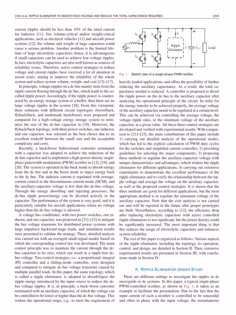
Fig. 1. Sketch view of a single-phase PWM rectifier.
heavily loaded applications, and offers the possibility of furtherreducing the auxiliary capacitance. As a result, the total ca-pacitance needed is reduced. A controller is proposed to divertthe ripple power on the dc bus to the auxiliary capacitor afteranalyzing the operational principle of the circuit. In order forthe energy transfer to be achieved properly, the average voltageof the auxiliary capacitor needs to be regulated at a certain level.This can be achieved via controlling the average voltage, thevoltage ripple ratio, or the minimum voltage of the auxiliarycapacitor, at a given value. All these three control strategies aredeveloped and verified with experimental results. With compar-ison to [21]–[23], the main contributions of this paper include1) carrying out detailed analysis of the operational modes,which has led to the explicit calculation of PWM duty cyclesfor the switches and simplified current controller; 2) providingguidelines for selecting the major components; 3) proposingthree methods to regulate the auxiliary-capacitor voltage withunique characteristics and advantages, which widens the rippleeliminator for different applications; 4) carrying out extensiveexperiments to demonstrate the excellent performance of theripple eliminator and to verify the relationship between the rip-ple voltage and average the voltage on the auxiliary capacitor,as well as the proposed control strategies. It is shown that thethree methods are good for different applications, but the mostappropriate method is to regulate the minimum voltage of theauxiliary capacitor. Note that the cost analysis is not carriedout and will be reported in the future after proper prototypesare built. Nevertheless, according to [12], the efficiency dropafter replacing electrolytic capacitors with active controlledripple eliminators is not significant, but the power density couldbe significantly increased. The most important thing is thatthis reduces the usage of electrolytic capacitors and enhancessystem reliability.
The rest of this paper is organized as follows: Various aspectsof the ripple eliminator, including the topology, its operation,control, and design, are detailed in Section II. Then, extensiveexperimental results are presented in Section III, with conclu-sions made in Section IV.
II. RIPPLE ELIMINATOR UNDER STUDY
There are different settings to investigate the ripples in dcmicrogrids or dc systems. In this paper, a typical single-phasePWM-controlled rectifier, as shown in Fig. 1, is taken as anexample to facilitate the presentation. Due to the fact that theinput current of such a rectifier is controlled to be sinusoidaland often in phase with the input voltage, the instantaneous

2226 IEEE TRANSACTIONS ON INDUSTRIAL ELECTRONICS, VOL. 62, NO. 4, APRIL 2015
Fig. 2. Ripple eliminator under study.
power taken at the ac side is pulsating, but the power consumedby the load at the dc side is often a constant (ideally). Thedifference of the two is called the ripple power. If there arecapacitors on the dc bus, then the ripple power should be takenby the capacitors, which leads to voltage ripples on the dc busbecause the capacitance cannot be infinite. In order to analyzethe voltage ripples of the dc bus, the net change of the energystored in the dc-bus capacitor over a charging period (i.e., aquarter cycle of the supply), which is called the ripple energy,can be calculated, as demonstrated in [12], as
Er =
√P 2o +
[ωLP 2
o
V 2s cos2 φ − Po
(sinφcosφ
)]2ω
(1)
where φ is the phase difference between the voltage and thecurrent of the ac supply. When the input current is in phasewith the voltage, φ = 0. In this case, the ripple energy is
Er =Isω
√V 2s + (ωLIs)2. (2)
When Er is high, the dc-bus capacitor needed can be very largein order to maintain the ripples below a certain level.
In recent years, there have been a lot of interests in divertingthe ripple power away from the dc bus into another energystorage device or a buffer, as mentioned before. Due to the factthat the voltage of the buffer is allowed to vary in a much widerrange without affecting the proper operation of the system,the capacitance needed can be considerably reduced. Such astrategy, called a ripple eliminator, is studied in this paper.
Although the PWM-controlled rectifier is taken as an ex-ample in this paper to facilitate the presentation, the strategystudied can be applied to other dc systems, e.g., inverterspowered by fuel cells or batteries and other dc systems thatare interfaced with an ac source/sink, without changing thetopology. The only change that may be needed is the way ofdetecting the ripple current flowing through the dc bus.
A. Topology
The proposed ripple eliminator to divert the ripple poweraway from the dc bus into another energy storage device isshown in Fig. 2. It is, in principle, a buck–boost converterterminated with an auxiliary capacitor Ca, which is operatedas the energy storage device or the buffer for the ripple power.
The inductor La is operated as an energy-transferring devicebetween the dc bus and the auxiliary capacitor.
In order to eliminate the voltage ripples on the dc bus, allthe ripple power should be diverted to the auxiliary capacitorCa. In other words, the current I needs to be maintained purelyconstant, and the ripple current ir in the dc-bus current i shouldflow or be diverted through the ripple eliminator. Since ir is anac current, diverting ir through the ripple eliminator involvestwo operating modes: charging and discharging the auxiliarycapacitor Ca. The inductor current should be controlled in theaverage-current mode, so that the current ir is at the right value.The ripple eliminator is operated in the DCM in this paperbecause the duty cycle of PWM for power switches in this casecan be calculated directly as demonstrated later and there is noneed to measure the inductor current for control purposes, whichsaves one current sensor and simplifies the controller design.
Since this ripple eliminator is a buck–boost converter in boththe charging mode and the discharging mode, the voltage acrossCa can be lower or higher than the dc-bus voltage. When itis controlled to be higher than the dc-bus voltage, it offers thepossibility of further reducing the capacitance Ca because theenergy stored in the capacitor is (1/2)CaV
2a0 and the ripple
energy corresponding to the voltage ripple ΔVa is
1
2Ca
(Va0+
1
2ΔVa
)2
− 1
2Ca
(Va0−
1
2ΔVa
)2
=CaVa0ΔVa.
(3)
For a given required ripple energy, e.g., Er, the larger theVa0, the smaller the Ca; the larger the voltage ripple ΔVa,the smaller the Ca. When Va0 is fixed, then Ca is in inverseproportion to ΔVa. Hence, this ripple eliminator allows theauxiliary capacitance Ca or the voltage ripple ΔVa on Ca tobe reduced considerably via increasing the voltage Va0. Oncethe ripple energy is diverted to Ca, the dc-bus capacitor is onlyneeded to deal with the ripples caused by the high-frequencyswitching. As a result, both C and Ca can be made small, so thatit is possible to use film capacitors instead of electrolytic capac-itors, which significantly enhances the reliability of the system[16]. Moreover, because of the high switching frequency forQ1 and Q2, the inductor La can be made very small as well.Hence, the ripple eliminator can be made very small and of highpower density. Note that the ripple eliminator can be sealed inone package, so that the high-voltage part of the circuit is notaccessible.
Without looking closely, the topology seems very similarto the one studied in [12]. However, it is different because1) the topology studied in [12] is operated as a buck converter inthe charging mode and as a boost converter in the dischargingmode; 2) the voltage across the auxiliary capacitor in [12] has tobe lower than the dc-bus voltage, and it is impossible to furtherreduce the auxiliary capacitor Ca by increasing the voltage levelof the auxiliary capacitor. The strategy proposed in this paper isable to halve the dc-bus voltage ripples with the same hardware,as demonstrated by the experimental results later.
B. Operation in the Charging Mode
When ir is positive, the ripple eliminator works in thecharging mode and transfers the ripple energy from the dc bus
CAO et al.: RIPPLE ELIMINATOR TO SMOOTH BUS VOLTAGE AND REDUCE THE TOTAL CAPACITANCE REQUIRED 2227
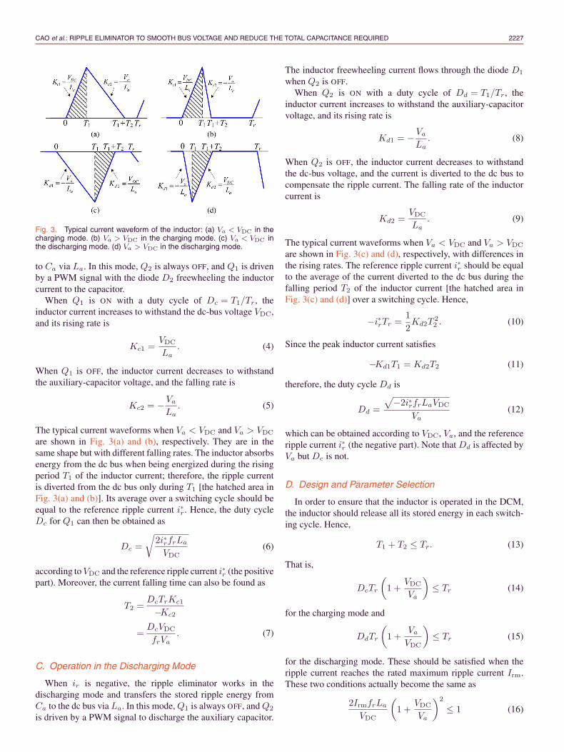
Fig. 3. Typical current waveform of the inductor: (a) Va < VDC in thecharging mode. (b) Va > VDC in the charging mode. (c) Va < VDC inthe discharging mode. (d) Va > VDC in the discharging mode.
to Ca via La. In this mode, Q2 is always OFF, and Q1 is drivenby a PWM signal with the diode D2 freewheeling the inductorcurrent to the capacitor.
When Q1 is ON with a duty cycle of Dc = T1/Tr, theinductor current increases to withstand the dc-bus voltage VDC,and its rising rate is
Kc1 =VDC
La. (4)
When Q1 is OFF, the inductor current decreases to withstandthe auxiliary-capacitor voltage, and the falling rate is
Kc2 = −Va
La. (5)
The typical current waveforms when Va < VDC and Va > VDC
are shown in Fig. 3(a) and (b), respectively. They are in thesame shape but with different falling rates. The inductor absorbsenergy from the dc bus when being energized during the risingperiod T1 of the inductor current; therefore, the ripple currentis diverted from the dc bus only during T1 [the hatched area inFig. 3(a) and (b)]. Its average over a switching cycle should beequal to the reference ripple current i∗r. Hence, the duty cycleDc for Q1 can then be obtained as
Dc =
√2i∗rfrLa
VDC(6)
according toVDC and the reference ripple current i∗r (the positivepart). Moreover, the current falling time can also be found as
T2 =DcTrKc1
−Kc2
=DcVDC
frVa. (7)
C. Operation in the Discharging Mode
When ir is negative, the ripple eliminator works in thedischarging mode and transfers the stored ripple energy fromCa to the dc bus via La. In this mode, Q1 is always OFF, and Q2
is driven by a PWM signal to discharge the auxiliary capacitor.
The inductor freewheeling current flows through the diode D1
when Q2 is OFF.When Q2 is ON with a duty cycle of Dd = T1/Tr, the
inductor current increases to withstand the auxiliary-capacitorvoltage, and its rising rate is
Kd1 = −Va
La. (8)
When Q2 is OFF, the inductor current decreases to withstandthe dc-bus voltage, and the current is diverted to the dc bus tocompensate the ripple current. The falling rate of the inductorcurrent is
Kd2 =VDC
La. (9)
The typical current waveforms when Va < VDC and Va > VDC
are shown in Fig. 3(c) and (d), respectively, with differences inthe rising rates. The reference ripple current i∗r should be equalto the average of the current diverted to the dc bus during thefalling period T2 of the inductor current [the hatched area inFig. 3(c) and (d)] over a switching cycle. Hence,
−i∗rTr =1
2Kd2T
22 . (10)
Since the peak inductor current satisfies
−Kd1T1 = Kd2T2 (11)
therefore, the duty cycle Dd is
Dd =
√−2i∗rfrLaVDC
Va(12)
which can be obtained according to VDC, Va, and the referenceripple current i∗r (the negative part). Note that Dd is affected byVa but Dc is not.
D. Design and Parameter Selection
In order to ensure that the inductor is operated in the DCM,the inductor should release all its stored energy in each switch-ing cycle. Hence,
T1 + T2 ≤ Tr. (13)
That is,
DcTr
(1 +
VDC
Va
)≤ Tr (14)
for the charging mode and
DdTr
(1 +
Va
VDC
)≤ Tr (15)
for the discharging mode. These should be satisfied when theripple current reaches the rated maximum ripple current Irm.These two conditions actually become the same as
2IrmfrLa
VDC
(1 +
VDC
Va
)2
≤ 1 (16)
2228 IEEE TRANSACTIONS ON INDUSTRIAL ELECTRONICS, VOL. 62, NO. 4, APRIL 2015
Fig. 4. Selection of (IrmfrLa)/VDC: between the two surfacesV 2a /(2(Va + VDC)
2) and 2(Irm/ILp)2.
which is equivalent to
La
VDC≤ V 2
a
2Irmfr(Va + VDC)2. (17)
Moreover, the inductor peak current should be maintainedbelow the maximum peak current ILp of the inductor. That is
DcTrVDC
La≤ ILp (18)
for the charging mode and
DdTrVa
La≤ ILp (19)
for the discharging mode. These should be satisfied when theripple current reaches the rated maximum ripple current Irmand the inductor current reaches the maximum peak currentILp. In this case, these two conditions become the same as
2IrmfrI2Lp
≤ La
VDC. (20)
Combining it with (17), there is
2IrmfrI2Lp
≤ La
VDC≤ V 2
a
2Irmfr(Va + VDC)2. (21)
This can be rewritten as
2
(IrmILp
)2
≤ IrmfrLa
VDC≤ V 2
a
2(Va + VDC)2(22)
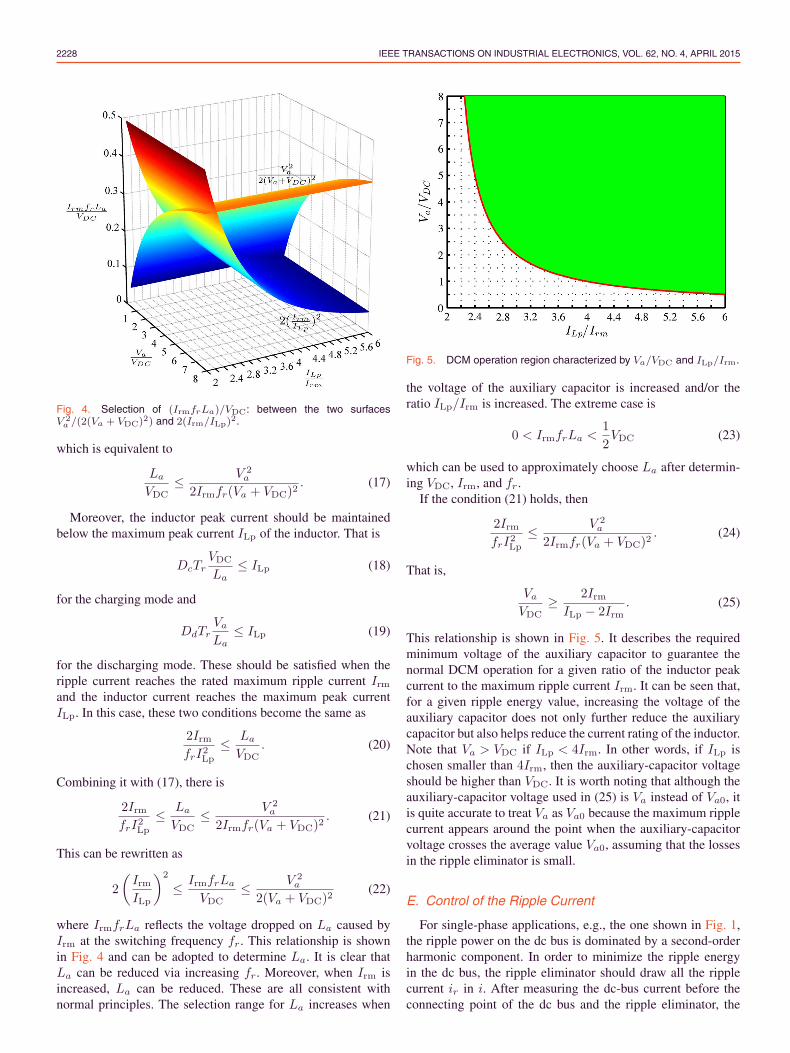
where IrmfrLa reflects the voltage dropped on La caused byIrm at the switching frequency fr. This relationship is shownin Fig. 4 and can be adopted to determine La. It is clear thatLa can be reduced via increasing fr. Moreover, when Irm isincreased, La can be reduced. These are all consistent withnormal principles. The selection range for La increases when
Fig. 5. DCM operation region characterized by Va/VDC and ILp/Irm.
the voltage of the auxiliary capacitor is increased and/or theratio ILp/Irm is increased. The extreme case is
0 < IrmfrLa <1
2VDC (23)
which can be used to approximately choose La after determin-ing VDC, Irm, and fr.
If the condition (21) holds, then
2IrmfrI2Lp
≤ V 2a
2Irmfr(Va + VDC)2. (24)
That is,
Va
VDC≥ 2Irm
ILp − 2Irm. (25)
This relationship is shown in Fig. 5. It describes the requiredminimum voltage of the auxiliary capacitor to guarantee thenormal DCM operation for a given ratio of the inductor peakcurrent to the maximum ripple current Irm. It can be seen that,for a given ripple energy value, increasing the voltage of theauxiliary capacitor does not only further reduce the auxiliarycapacitor but also helps reduce the current rating of the inductor.Note that Va > VDC if ILp < 4Irm. In other words, if ILp ischosen smaller than 4Irm, then the auxiliary-capacitor voltageshould be higher than VDC. It is worth noting that although theauxiliary-capacitor voltage used in (25) is Va instead of Va0, itis quite accurate to treat Va as Va0 because the maximum ripplecurrent appears around the point when the auxiliary-capacitorvoltage crosses the average value Va0, assuming that the lossesin the ripple eliminator is small.
E. Control of the Ripple Current
For single-phase applications, e.g., the one shown in Fig. 1,the ripple power on the dc bus is dominated by a second-orderharmonic component. In order to minimize the ripple energyin the dc bus, the ripple eliminator should draw all the ripplecurrent ir in i. After measuring the dc-bus current before theconnecting point of the dc bus and the ripple eliminator, the

CAO et al.: RIPPLE ELIMINATOR TO SMOOTH BUS VOLTAGE AND REDUCE THE TOTAL CAPACITANCE REQUIRED 2229
Fig. 6. Control strategy for the ripple eliminator.
second-order harmonic component can be obtained via passingthe current i through the resonant filter [15], [24]
KR(s) =2ξhωs
s2 + 2ξhωs+ (hω)2(26)
where h = 2 and ω = 2πf . In order to cope with frequencyvariations, ξ can be chosen as 0.01–0.02. Once the ripplecurrent is obtained, the duty cycles in the charging mode andin the discharging mode can be calculated from (6) and (12)to generate the gate signals gQ1 and gQ2, respectively. Theresulting control strategy is shown in Fig. 6, with the injectionof an additional dc bias current I∗a that is needed to establishand maintain a stable auxiliary-capacitor voltage, which is tobe discussed in the next subsection. If the ripple current is notdominated by a second-order harmonic component, then KR(s)needs to be changed accordingly.
F. Control of the Auxiliary-Capacitor Voltage
Since the voltage ripples on the dc bus are transferred to theauxiliary capacitor, there are significant ripples in the voltageVa. Its dc component Va0 can be obtained after passing thevoltage Va through the hold filter
H(s) =1− e−Ts/2
Ts/2(27)
because the fundamental frequency of the ripple is twice ofthe ac supply frequency T = 1/f . In order to maintain theauxiliary-capacitor voltage, three control methods are proposedin this paper to meet different requirements.
1) Method A: To Maintain Va0 at a Given Value V ∗a0:
This is the most straightforward requirement and can be easilyachieved with a PI controller, after comparing the dc componentVa0 with the given value V ∗
a0. As a result, the PI controllergenerates the required dc bias current I∗a to charge the auxiliarycapacitor. The resulting controller is shown in Fig. 7(a). Theinput of the PI controller is the difference of the auxiliary-capacitor voltage from the given value V ∗
a0, and the output isthe additional current I∗a to be injected to the ripple eliminator,i.e., the dc offset of the reference ripple current i∗r. The tuningof the PI controller can be started with a proportional gain KP
to achieve the expected time constant Tc of the loop from I∗a toV ∗a0, which is approximately
Tc =Ca
Kp.
Fig. 7. Regulation of the auxiliary-capacitor voltage to generate I∗a .(a) Method A: To maintain a given average voltage V ∗
a0. (b) Method B:to maintain a given ripple ratio R∗
v . (c) Method C: to maintain a givenminimum voltage V ∗
amin.
The integral gain can then be chosen initially to be the same asKp. If needed, some fine tuning through trial and error can becarried out. In practice, a small Tc may lead to a large chargingcurrent that might trigger the current protection.
If the ripple energy increases, then the voltage ripple ΔVa
on the auxiliary capacitor would increase as well according to(3). This would cause the minimum voltage Vamin to decreaseaccordingly. When Vamin decreases below a certain level, theripple energy could not be compensated sufficiently. Therefore,the given average voltage V ∗
a0 should be chosen high enoughto cope with the variation of ripple energy on the dc bus.An indicative value for Vamin can be obtained from (25) as(2Irm/ILp − 2Irm)VDC; see the experimental verification inSection III-B. This is often not an issue because the idea ofripple eliminators is to increase V ∗
a0 as much as practicallypossible.
2) Method B: To Maintain a Given Ripple Ratio R∗v
for Va: As illustrated in [25]–[27], increased voltage rippleslead to increased capacitor currents, which accelerates the agingprocess of the capacitor. Hence, for applications with high-voltage ripples, it is better to maintain the voltage ripple ratiowithin a certain range, so that the capacitor current is limited.This is beneficial to extend the life cycle of the auxiliarycapacitor.

2230 IEEE TRANSACTIONS ON INDUSTRIAL ELECTRONICS, VOL. 62, NO. 4, APRIL 2015
The ripple ratio Rv of Va is the ratio of the ripple amplitudeΔVa (peak to peak) to the average voltage Va0, i.e.,
Rv =ΔVa
Va0× 100%. (28)
In order to improve the performance under different loadingconditions, the ripple ratio of Va can be maintained, so that theaverage voltage Va0 can be automatically regulated when theload changes. This can be achieved with the strategy shown inFig. 7(b), where the resonant filter (26) is adopted to pick upthe voltage ripples in Va so that the peak-to-peak value can beobtained as ΔVa. Due to the scaling factor from the voltage Va
to the ripple ratio R∗v, the parameters of the PI controller can be
obtained by scaling the parameters of the PI controller used inMethod A by Va0/R
∗v as the starting point of the tuning process.
Since the order of the system is low, the range of the parametersis very wide, which makes it very easy to tune the parameters.
Substituting (28) into (3), the corresponding ripple energythat the auxiliary capacitor handles is RvCaV
2a0. For a desired
Va0, the ripple ratio increases with the ripple energy. Hence,Method B is good for systems with high ripple energy, andMethod A is good for systems with low ripple energy.
3) Method C: To Maintain a Given Minimum VoltageV ∗amin for Va: As discussed earlier, in order to maintain the
normal operation of the ripple eliminator in the DCM, thevoltage of the auxiliary capacitor should be controlled to behigher than a certain value. It is then natural to regulate Va,so that it is higher than a minimum voltage V ∗
amin. This can beachieved with the strategy shown in Fig. 7(c), where the rippleratio R∗
v in Method B is automatically adjusted according to theoperational condition as
R∗v = 2
(1− V ∗
amin
Va0
). (29)
By doing this, the voltage stress of the auxiliary capacitor canbe kept at the minimum, while maintaining good performanceunder different load conditions. The parameters of the PI con-troller can be chosen the same as the ones for Method B becausethe only change is to set the reference R∗
v as a specific valuegiven in (29).
The difference from Method B is that the minimum voltageis kept constant and the ripple ratio changes here when the loadchanges, but with Method B, the ripple ratio is kept constantand the minimum voltage changes. In other words, Method Cactually keeps the minimum voltage stress on the auxiliarycapacitor without affecting the current tracking performance.In addition, maintaining the minimum voltage can reduce theoperating voltage of the capacitor. Therefore, the voltage ratingof the capacitor needed in the ripple eliminator can be reducedaccordingly. In summary, Method C is the most appropriate oneamong the three methods.
III. EXPERIMENTAL RESULTS
In order to verify the proposed strategy, some experimentswere carried out with a 1-kW prototype. The test rig consistsof a single-phase PWM-controlled rectifier and the ripple elim-inator, as shown in Fig. 8. The rectifier and the ripple elimi-nator were controlled separately using two TI TMS320F28335
Fig. 8. Overall control schematic of the test rig.
TABLE IPARAMETERS OF THE EXPERIMENTAL SYSTEM
Fig. 9. Experimental results of the PWM-controlled rectifier.
without any communication. The parameters of the systemare listed in Table I. In order to demonstrate the effective-ness of the ripple eliminator later, experiments were carriedout on the test rig without the ripple eliminator at first. Theresults are shown in Fig. 9. The input current is in phase withthe input voltage, but the voltage ripple on the dc bus is 78 V.
A. Performance of the Strategy in [12]
In order to demonstrate the performance of the ripple elimi-nator, the experimental system was reconfigured according to
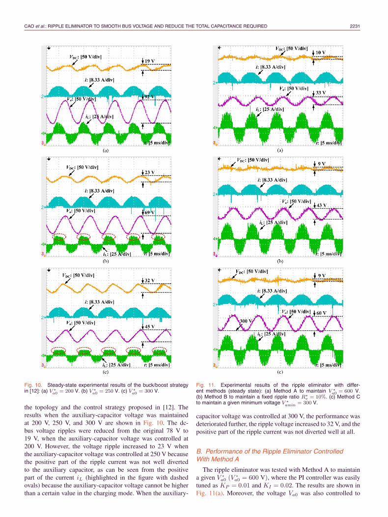
CAO et al.: RIPPLE ELIMINATOR TO SMOOTH BUS VOLTAGE AND REDUCE THE TOTAL CAPACITANCE REQUIRED 2231
Fig. 10. Steady-state experimental results of the buck/boost strategyin [12]: (a) V ∗
a0 = 200 V. (b) V ∗a0 = 250 V. (c) V ∗
a0 = 300 V.
the topology and the control strategy proposed in [12]. Theresults when the auxiliary-capacitor voltage was maintainedat 200 V, 250 V, and 300 V are shown in Fig. 10. The dc-bus voltage ripples were reduced from the original 78 V to19 V, when the auxiliary-capacitor voltage was controlled at200 V. However, the voltage ripple increased to 23 V whenthe auxiliary-capacitor voltage was controlled at 250 V becausethe positive part of the ripple current was not well divertedto the auxiliary capacitor, as can be seen from the positivepart of the current iL (highlighted in the figure with dashedovals) because the auxiliary-capacitor voltage cannot be higherthan a certain value in the charging mode. When the auxiliary-
Fig. 11. Experimental results of the ripple eliminator with differ-ent methods (steady state): (a) Method A to maintain V ∗
a0 = 600 V.(b) Method B to maintain a fixed ripple ratio R∗
v = 10%. (c) Method Cto maintain a given minimum voltage V ∗
amin = 300 V.
capacitor voltage was controlled at 300 V, the performance wasdeteriorated further, the ripple voltage increased to 32 V, and thepositive part of the ripple current was not diverted well at all.
B. Performance of the Ripple Eliminator ControlledWith Method A
The ripple eliminator was tested with Method A to maintaina given V ∗
a0 (V ∗a0 = 600 V), where the PI controller was easily
tuned as KP = 0.01 and KI = 0.02. The results are shown inFig. 11(a). Moreover, the voltage Va0 was also controlled to
2232 IEEE TRANSACTIONS ON INDUSTRIAL ELECTRONICS, VOL. 62, NO. 4, APRIL 2015
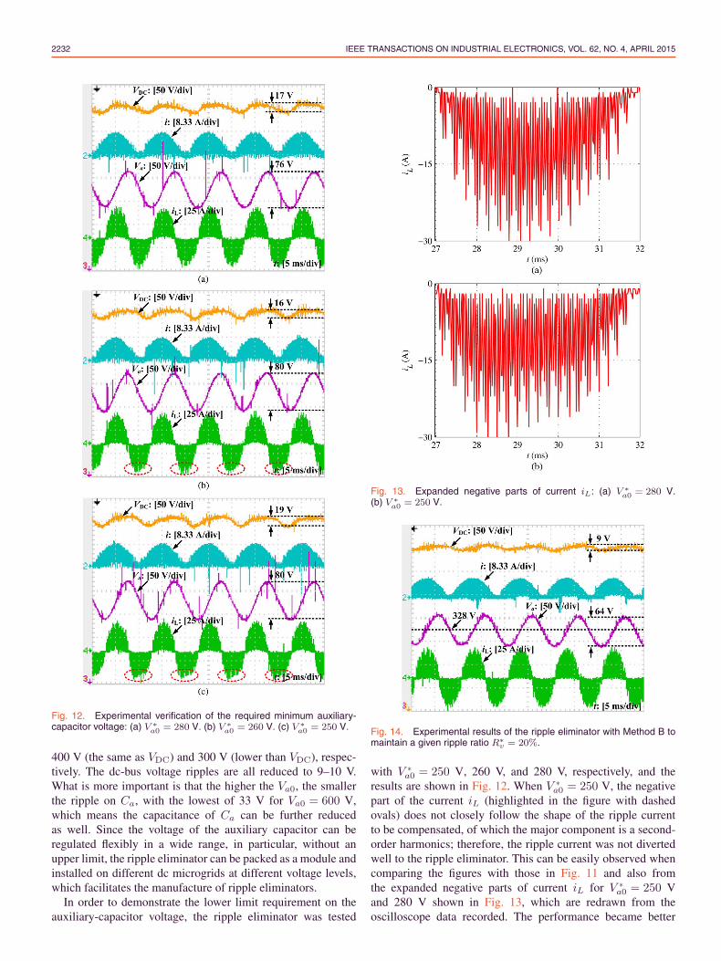
Fig. 12. Experimental verification of the required minimum auxiliary-capacitor voltage: (a) V ∗
a0 = 280 V. (b) V ∗a0 = 260 V. (c) V ∗
a0 = 250 V.
400 V (the same as VDC) and 300 V (lower than VDC), respec-tively. The dc-bus voltage ripples are all reduced to 9–10 V.What is more important is that the higher the Va0, the smallerthe ripple on Ca, with the lowest of 33 V for Va0 = 600 V,which means the capacitance of Ca can be further reducedas well. Since the voltage of the auxiliary capacitor can beregulated flexibly in a wide range, in particular, without anupper limit, the ripple eliminator can be packed as a module andinstalled on different dc microgrids at different voltage levels,which facilitates the manufacture of ripple eliminators.
In order to demonstrate the lower limit requirement on theauxiliary-capacitor voltage, the ripple eliminator was tested
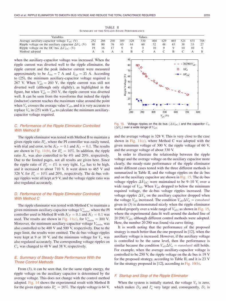
Fig. 13. Expanded negative parts of current iL: (a) V ∗a0 = 280 V.
(b) V ∗a0 = 250 V.
Fig. 14. Experimental results of the ripple eliminator with Method B tomaintain a given ripple ratio R∗
v = 20%.
with V ∗a0 = 250 V, 260 V, and 280 V, respectively, and the
results are shown in Fig. 12. When V ∗a0 = 250 V, the negative
part of the current iL (highlighted in the figure with dashedovals) does not closely follow the shape of the ripple currentto be compensated, of which the major component is a second-order harmonics; therefore, the ripple current was not divertedwell to the ripple eliminator. This can be easily observed whencomparing the figures with those in Fig. 11 and also fromthe expanded negative parts of current iL for V ∗
a0 = 250 Vand 280 V shown in Fig. 13, which are redrawn from theoscilloscope data recorded. The performance became better
CAO et al.: RIPPLE ELIMINATOR TO SMOOTH BUS VOLTAGE AND REDUCE THE TOTAL CAPACITANCE REQUIRED 2233
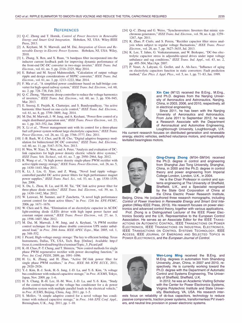
TABLE IISUMMARY OF THE STEADY-STATE PERFORMANCE
when the auxiliary-capacitor voltage was increased. When theripple current was diverted well to the ripple eliminator, theripple current and the peak inductor current were measuredapproximately to be Irm = 7 A and ILp = 35 A. Accordingto (25), the minimum auxiliary-capacitor voltage required is267 V. When V ∗
a0 = 260 V, the ripple current was still notdiverted well (although only slightly), as highlighted in thefigure, but when V ∗
a0 = 280 V, the ripple current was divertedwell. It can be seen from the waveforms that indeed the ripple(inductor) current reaches the maximum value around the pointwhen Va crosses the average value Va0, and it is very accurate toreplace Va in (25) with Va0 to calculate the minimum auxiliary-capacitor voltage required.
C. Performance of the Ripple Eliminator ControlledWith Method B
The ripple eliminator was tested with Method B to maintain agiven ripple ratio R∗
v , where the PI controller was easily tuned,with trial and error, to be KP = 0.1 and KI = 0.1. The resultsare shown in Fig. 11(b), for R∗
v = 10%. In addition, the rippleratio Rv was also controlled to be 4% and 20%, respectively.Due to the limited pages, not all results are given here. Sincethe ripple ratio of R∗
v = 4% is very tight, Va0 has to be high,and it increased to about 710 V. It went down to 465 V and328 V, for R∗
v = 10% and 20%, respectively. The dc-bus volt-age ripples were all kept at 9 V, and the voltage ripple ratio wasalso regulated accurately.
D. Performance of the Ripple Eliminator ControlledWith Method C
The ripple eliminator was tested with Method C to maintain agiven minimum auxiliary-capacitor voltage V ∗
amin, where the PIcontroller used in Method B with KP = 0.1 and KI = 0.1 wasused. The results are shown in Fig. 11(c), for V ∗
amin = 300 V.Moreover, the minimum auxiliary-capacitor voltage Vamin wasalso controlled to be 400 V and 500 V, respectively. Due to thepage limit, the results were omitted. The dc-bus voltage rippleswere kept at 9 or 10 V, and the minimum voltage for Va wasalso regulated accurately. The corresponding voltage ripples onCa was changed to 48 V and 38 V, respectively.
E. Summary of Steady-State Performance With theThree Control Methods
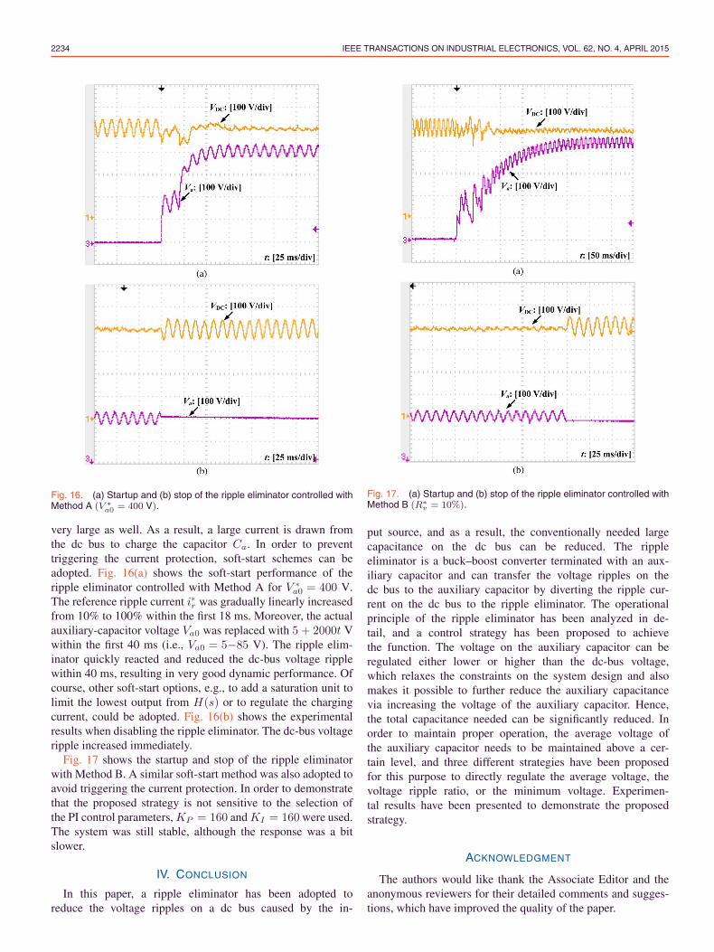
From (3), it can be seen that, for the same ripple energy, theripple voltage on the auxiliary capacitor is determined by theaverage voltage. This does not change with the control methodadopted. Fig. 14 shows the experimental result with Method Bfor the given ripple ratio R∗
v = 20%. The ripple voltage is 64 V,
Fig. 15. Voltage ripples on the dc bus (ΔVDC) and the capacitor Ca
(ΔVa) over a wide range of Va0.
and the average voltage is 328 V. This is very close to the caseshown in Fig. 11(c), where Method C was adopted with thegiven minimum voltage of 300 V, the ripple voltage of 60 V,and the average voltage of about 330 V.
In order to illustrate the relationship between the ripplevoltage and the average voltage on the auxiliary capacitor moreclearly, the steady-state performance of the ripple eliminatorunder different cases tested with the three different methods issummarized in Table II, and the voltage ripples on the dc busand on the auxiliary capacitor are shown in Fig. 15. The dc-busvoltage ripples ΔVDC were maintained to be 9–10 V, over awide range of Va0. When Va0 dropped to below the minimumrequired voltage, the dc-bus voltage ripples increased. Thevoltage ripples ΔVa on the auxiliary capacitor dropped whenthe voltage Va0 increased. The condition Va0ΔVa = constantgiven in (3) is demonstrated nicely when the ripple eliminatorworked properly over a wide range of Va0, as shown in Fig. 15,where the experimental data fit well around the dashed line of20 290/Va0, although different control methods were adopted.Here, the number 20 290 was found via curve fitting.
It is worth noting that the performance of the proposedstrategy is much better than the one proposed in [12], when theauxiliary voltage is increased. However, if the auxiliary voltageis controlled to be the same level, then the performance issimilar because the condition Va0ΔVa = constant still holds.For example, when the average auxiliary-capacitor voltage iscontrolled to be 250 V, the ripple voltage on the dc bus is 19 Vfor the proposed strategy, according to Table II, and it is 23 Vfor the strategy proposed in [12], according to Fig. 10(b).
F. Startup and Stop of the Ripple Eliminator
When the system is initially started, the voltage Va is zero,which makes Dd and I∗a very large and, consequently, Dc is
2234 IEEE TRANSACTIONS ON INDUSTRIAL ELECTRONICS, VOL. 62, NO. 4, APRIL 2015
Fig. 16. (a) Startup and (b) stop of the ripple eliminator controlled withMethod A (V ∗
a0 = 400 V).
very large as well. As a result, a large current is drawn fromthe dc bus to charge the capacitor Ca. In order to preventtriggering the current protection, soft-start schemes can beadopted. Fig. 16(a) shows the soft-start performance of theripple eliminator controlled with Method A for V ∗
a0 = 400 V.The reference ripple current i∗r was gradually linearly increasedfrom 10% to 100% within the first 18 ms. Moreover, the actualauxiliary-capacitor voltage Va0 was replaced with 5 + 2000t Vwithin the first 40 ms (i.e., Va0 = 5−85 V). The ripple elim-inator quickly reacted and reduced the dc-bus voltage ripplewithin 40 ms, resulting in very good dynamic performance. Ofcourse, other soft-start options, e.g., to add a saturation unit tolimit the lowest output from H(s) or to regulate the chargingcurrent, could be adopted. Fig. 16(b) shows the experimentalresults when disabling the ripple eliminator. The dc-bus voltageripple increased immediately.
Fig. 17 shows the startup and stop of the ripple eliminatorwith Method B. A similar soft-start method was also adopted toavoid triggering the current protection. In order to demonstratethat the proposed strategy is not sensitive to the selection ofthe PI control parameters, KP = 160 and KI = 160 were used.The system was still stable, although the response was a bitslower.
IV. CONCLUSION
In this paper, a ripple eliminator has been adopted toreduce the voltage ripples on a dc bus caused by the in-
Fig. 17. (a) Startup and (b) stop of the ripple eliminator controlled withMethod B (R∗
v = 10%).
put source, and as a result, the conventionally needed largecapacitance on the dc bus can be reduced. The rippleeliminator is a buck–boost converter terminated with an aux-iliary capacitor and can transfer the voltage ripples on thedc bus to the auxiliary capacitor by diverting the ripple cur-rent on the dc bus to the ripple eliminator. The operationalprinciple of the ripple eliminator has been analyzed in de-tail, and a control strategy has been proposed to achievethe function. The voltage on the auxiliary capacitor can beregulated either lower or higher than the dc-bus voltage,which relaxes the constraints on the system design and alsomakes it possible to further reduce the auxiliary capacitancevia increasing the voltage of the auxiliary capacitor. Hence,the total capacitance needed can be significantly reduced. Inorder to maintain proper operation, the average voltage ofthe auxiliary capacitor needs to be maintained above a cer-tain level, and three different strategies have been proposedfor this purpose to directly regulate the average voltage, thevoltage ripple ratio, or the minimum voltage. Experimen-tal results have been presented to demonstrate the proposedstrategy.
ACKNOWLEDGMENT
The authors would like thank the Associate Editor and theanonymous reviewers for their detailed comments and sugges-tions, which have improved the quality of the paper.
CAO et al.: RIPPLE ELIMINATOR TO SMOOTH BUS VOLTAGE AND REDUCE THE TOTAL CAPACITANCE REQUIRED 2235
REFERENCES
[1] Q.-C. Zhong and T. Hornik, Control of Power Inverters in RenewableEnergy and Smart Grid Integration. Hoboken, NJ, USA: Wiley-IEEEPress, 2013.
[2] A. Keyhani, M. N. Marwali, and M. Dai, Integration of Green and Re-newable Energy in Electric Power Systems. Hoboken, NJ, USA: Wiley,2010.
[3] L. Zhang, X. Ren, and X. Ruan, “A bandpass filter incorporated into theinductor current feedback path for improving dynamic performance ofthe front-end DC-DC converter in two-stage inverter,” IEEE Trans. Ind.Electron., vol. 61, no. 5, pp. 2316–2325, May 2014.
[4] E. Babaei and M. Seyed Mahmoodieh, “Calculation of output voltageripple and design considerations of SEPIC converter,” IEEE Trans. Ind.Electron., vol. 61, no. 3, pp. 1213–1222, Mar. 2014.
[5] F. Ma et al., “A simplified power conditioner based on half-bridge con-verter for high-speed railway system,” IEEE Trans. Ind. Electron., vol. 60,no. 2, pp. 728–738, Feb. 2013.
[6] Q.-C. Zhong, “Harmonic droop controller to reduce the voltage harmonicsof inverters,” IEEE Trans. Ind. Electron., vol. 60, no. 3, pp. 936–945,Mar. 2013.
[7] E. Sreeraj, E. Prejith, K. Chatterjee, and S. Bandyopadhyay, “An activeharmonic filter based on one-cycle control,” IEEE Trans. Ind. Electron.,vol. 61, no. 8, pp. 3799–3809, Aug. 2014.
[8] M. Dai, M. Marwali, J.-W. Jung, and A. Keyhani, “Power flow control of asingle distributed generation unit,” IEEE Trans. Power Electron., vol. 23,no. 1, pp. 343–352, Jan. 2008.
[9] X. Li et al., “Power management unit with its control for a three-phasefuel cell power system without large electrolytic capacitors,” IEEE Trans.Power Electron., vol. 26, no. 12, pp. 3766–3777, Dec. 2011.
[10] J.-B. Baek, W.-I. Choi, and B.-H. Cho, “Digital adaptive frequency mod-ulation for bidirectional DC-DC converter,” IEEE Trans. Ind. Electron.,vol. 60, no. 11, pp. 5167–5176, Nov. 2013.
[11] H. Wen, W. Xiao, X. Wen, and A. Peter, “Analysis and evaluation of DC-link capacitors for high power density electric vehicle drive systems,”IEEE Trans. Veh. Technol., vol. 61, no. 7, pp. 2950–2964, Sep. 2012.
[12] R. Wang et al., “A high power density single-phase PWM rectifier withactive ripple energy storage,” IEEE Trans. Power Electron., vol. 26, no. 5,pp. 1430–1443, May 2011.
[13] K. Li, J. Liu, G. Xiao, and Z. Wang, “Novel load ripple voltage-controlled parallel DC active power filters for high performance magnetpower supplies,” IEEE Trans. Nucl. Sci., vol. 53, no. 3, pp. 1530–1539,Jun. 2006.
[14] X. Du, L. Zhou, H. Lu, and H.-M. Tai, “DC link active power filter forthree-phase diode rectifier,” IEEE Trans. Ind. Electron., vol. 59, no. 3,pp. 1430–1442, Mar. 2012.
[15] W. Lenwari, M. Sumner, and P. Zanchetta, “A novel high performancecurrent control for shunt active filters,” in Proc. 12th Int. EPE-PEMC,2006, pp. 1671–1676.
[16] W. Chen and S. Hui, “Elimination of an electrolytic capacitor in AC/DClight-emitting diode (LED) driver with high input power factor andconstant output current,” IEEE Trans. Power Electron., vol. 27, no. 3,pp. 1598–1607, Mar. 2012.
[17] M. Dai, M. Marwali, J.-W. Jung, and A. Keyhani, “A PWM rectifiercontrol technique for three-phase double conversion UPS under unbal-anced load,” in Proc. 20th Annu. IEEE APEC Expo., Mar. 2005, vol. 1,pp. 548–552.
[18] J. Picard, High-voltage energy storage: The key to efficient holdup, TexasInstruments, Dallas, TX, USA, Tech. Rep. [Online]. Available: http://focus.ti.com/download/trng/docs/seminar/Topic_5_Picard.pdf
[19] K.-H. Chao, P.-T. Cheng, and T. Shimizu, “New control methods for singlephase PWM regenerative rectifier with power decoupling function,” inProc. Int. Conf. PEDS, 2009, pp. 1091–1096.
[20] H. Li, K. Zhang, and H. Zhao, “Active DC-link power filter forsingle phase PWM rectifiers,” in Proc. IEEE 8th ICPE ECCE, 2011,pp. 2920–2926.
[21] Y.-J. Kim, B.-J. Seok, H.-S. Jung, J.-D. La, and Y.-S. Kim, “A voltagebus conditioner with reduced capacitive storage,” in Proc. ICEMS, Tokyo,Japan, Nov. 2009, pp. 1–6.
[22] H. S. Chang, B.-H. Lee, H.-M. Woo, J.-D. La, and Y.-S. Kim, “Studyof the control technique of the voltage bus conditioner for a dc powerdistribution system with multiple parallel loads in the electrical vehicle,”in Proc. ICEMS, Beijing, China, Aug. 2011, pp. 1–5.
[23] S. Mollov, “A simple adaptive control for a novel voltage bus condi-tioner with reduced capacitive storage,” in Proc. 14th EPE Conf. Appl.,Birmingham, U.K., Aug. 2011, pp. 1–10.
[24] Q.-C. Zhong and G. Weiss, “Synchronverters: Inverters that mimic syn-chronous generators,” IEEE Trans. Ind. Electron., vol. 58, no. 4, pp. 1259–1267, Apr. 2011.
[25] K. Zhao, P. Ciufo, and S. Perera, “Rectifier capacitor filter stress anal-ysis when subject to regular voltage fluctuations,” IEEE Trans. PowerElectron., vol. 28, no. 7, pp. 3627–3635, Jul. 2013.
[26] K. Lee, T. Jahns, G. Venkataramanan, and W. Berkopec, “DC-bus elec-trolytic capacitor stress in adjustable-speed drives under input voltageunbalance and sag conditions,” IEEE Trans. Ind. Appl., vol. 43, no. 2,pp. 495–504, Mar./Apr. 2007.
[27] P. Venet, A. Lahyani, G. Grellet, and A. Ah-Jaco, “Influence of agingon electrolytic capacitors function in static converters: Fault predictionmethod,” Eur. Phys. J. Appl. Phys., vol. 5, no. 1, pp. 71–83, Jan. 1999.
Xin Cao (M’12) received the B.Eng., M.Eng.,and Ph.D. degrees from the Nanjing Univer-sity of Aeronautics and Astronautics, Nanjing,China, in 2003, 2006, and 2010, respectively, allin electrical engineering.
Since 2011, he has been with the NanjingUniversity of Aeronautics and Astronautics.From June 2011 to September 2012, he wasa Research Associate with the Departmentof Aeronautical and Automotive Engineering,Loughborough University, Loughborough, U.K.
His current research focuses on distributed generation and renewableenergy, electric vehicles, switched reluctance motors, and magneticallylevitated bearingless motors.
Qing-Chang Zhong (M’04–SM’04) receivedthe Ph.D. degree in control and engineeringfrom Shanghai Jiao Tong University, Shanghai,China, in 2000 and the Ph.D. degree in controltheory and power engineering from ImperialCollege London, London, U.K., in 2004.
He is the Chair Professor in control and sys-tems engineering at The University of Sheffield,Sheffield, U.K., and a Specialist recognizedby the State Grid Corporation of China atthe China Electric Power Research Institute,
Beijing, China. He (co)authored three research monographs, includingControl of Power Inverters in Renewable Energy and Smart Grid Inte-gration (Wiley-IEEE Press, 2013). His research focuses on power elec-tronics and advanced control theory, together with various applications.
Prof. Zhong is a Distinguished Lecturer of the IEEE Power Elec-tronics Society and the U.K. Representative to the European ControlAssociation. He serves as an Associate Editor for the IEEE TRANS-ACTIONS ON AUTOMATIC CONTROL, IEEE TRANSACTIONS ON POWERELECTRONICS, IEEE TRANSACTIONS ON INDUSTRIAL ELECTRONICS,IEEE TRANSACTIONS ON CONTROL SYSTEMS TECHNOLOGY, IEEEACCESS, IEEE JOURNAL OF EMERGING AND SELECTED TOPICS INPOWER ELECTRONICS, and the European Journal of Control.
Wen-Long Ming received the B.Eng. andM.Eng. degrees in automation from ShandongUniversity, Jinan, China, in 2007 and 2010, re-spectively. He is currently working toward thePh.D. degree with the Department of AutomaticControl and Systems Engineering, The Univer-sity of Sheffield, Sheffield, U.K.
In 2012, he was an Academic Visiting Scholarwith the Center for Power Electronics Systems,Virginia Polytechnic Institute and State Univer-sity, Blacksburg, VA, USA. His research inter-
ests focus on reliability of dc-bus capacitors, technology to reducepassive components, traction power systems, transformerless PV invert-ers, and neutral line provision in power electronic systems.