right pages of circuits & devices lab manual for ii sem ece & cse
TRANSCRIPT
5/12/2018 Right Pages of Circuits & Devices Lab Manual for II Sem Ece & Cse - slidepdf.com
http://slidepdf.com/reader/full/right-pages-of-circuits-devices-lab-manual-for-ii-sem-ece-cse 1/36
CIRCUITS AND DEVICES LAB MA
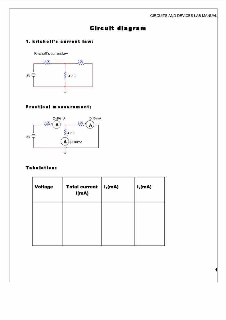
Circuit diagram
1. krichoff’s current law:
1.0kΩ 3.3kΩ
5V 4.7 K
Kirchoff`s current law
Practical measurement:
1.0kΩ 3.3kΩ
5V
4.7 K
A A
A
+ - + -
+
-
(0-20)mA (0-10)mA
(0-10)mA
Tabulation:
Voltage Total current
I(mA)
I1(mA) I2(mA)
5/12/2018 Right Pages of Circuits & Devices Lab Manual for II Sem Ece & Cse - slidepdf.com
http://slidepdf.com/reader/full/right-pages-of-circuits-devices-lab-manual-for-ii-sem-ece-cse 2/36
CIRCUITS AND DEVICES LAB MA
1.VERIFICATION OF KVL & KCL
AIM:
To verify (i) kirchoff’s current law (ii) kirchoff’s voltage law
(i) KIRCHOFF’S CURRENT LAW:
COMPONENTS REQUIRED:
Sl.No components Range Quantity
1
2
3
4
5
RPS
Resistor
Ammeter
Bread board
Connecting wires
(0-15)V
1 KΩ
(0-10)mA
------
------
1
3
3
1
few
THEORY:
krichoff’s current law:The algebraic sum of the currents entering in any node is Zero.
The law represents the mathematical statement of the fact change cannot accumulate at a node. A node is ncircuit element and it certainly cannot store destroy (or) generate charge. Hence the current must sum to zehydraulic analog sum is zero. For example consider three water pipes joined pn the shape of Y. we definedcurrents as following into each of 3 pipes. If we insists that what is always
PROCEDURE:
1. Connections are made as per the circuit diagram.
2. Check your connections before switch on the supply.3. Vary the regulated supply.4. Measure the current using ammeter.5. Note the readings in the tabulation.6. Compare the observation reading to theoretical value.
5/12/2018 Right Pages of Circuits & Devices Lab Manual for II Sem Ece & Cse - slidepdf.com
http://slidepdf.com/reader/full/right-pages-of-circuits-devices-lab-manual-for-ii-sem-ece-cse 3/36
CIRCUITS AND DEVICES LAB MA
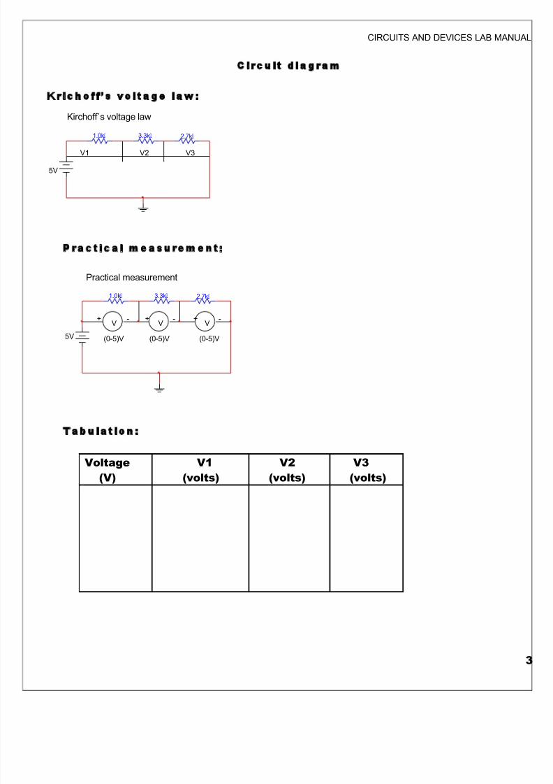
Circuit diagram
Krichoff’s voltage law:
Kirchoff`s voltage law
1.0kΩ 3.3kΩ 2.7kΩ
5V
V1 V2 V3
Practical measurement:
1.0kΩ 3.3kΩ 2.7kΩ
5V
V V V+ - + - + -
(0-5)V (0-5)V (0-5)V
Practical measurement
Tabulation:
Voltage
(V)
V1
(volts)
V2
(volts)
V3
(volts)
5/12/2018 Right Pages of Circuits & Devices Lab Manual for II Sem Ece & Cse - slidepdf.com
http://slidepdf.com/reader/full/right-pages-of-circuits-devices-lab-manual-for-ii-sem-ece-cse 4/36
CIRCUITS AND DEVICES LAB MA
ii) KIRCHOFF’S VOLTAGE LAW:
COMPONENTS REQUIRED:
Sl.No components Range Quantity
1
2
3
4
5
RPS
Resistor
voltmeter
Bread board
Connecting wires
(0-15)V
1KΩ,2.2KΩ,3.3KΩ
(0-20)V
------
------
1
Each 1
3
1
few
THEORY:
(i) krichoff’s voltage law
The algebraic sum of the voltage around any closed path is zero.
PROCEDURE:
1. Connections are made as per the circuit diagram.
2. Check your connections before switch on the supply.3. Vary the regulated supply.4. Measure the voltage using voltmeter.5. Note the readings in the tabulation.6. Compare the observation reading to theoretical value.
RESULT:
Thus the kirchoff’s current law and voltage law were verified.
5/12/2018 Right Pages of Circuits & Devices Lab Manual for II Sem Ece & Cse - slidepdf.com
http://slidepdf.com/reader/full/right-pages-of-circuits-devices-lab-manual-for-ii-sem-ece-cse 5/36
CIRCUITS AND DEVICES LAB MA
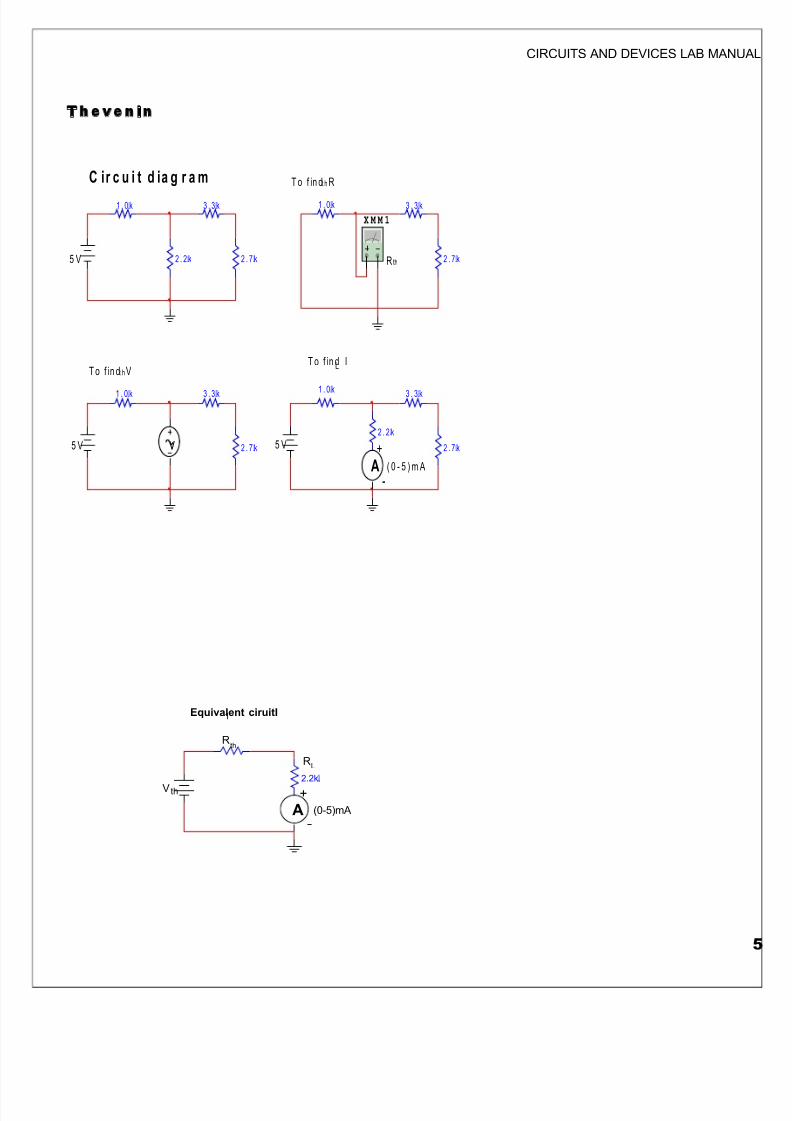
Thevenin
1 . 0 kΩ
2 . 2 kΩ
3 . 3 kΩ
C ir c u i t d ia g r a m
T o f in d Vt h
2 . 7 kΩ
1 . 0 kΩ 3 . 3 kΩ
2 . 7 kΩv
T o f in d Rt h
1 . 0 kΩ 3 . 3 kΩ
2 . 7 kΩ
X M M 1
R th
T o f in d IL
1 . 0 kΩ
2 . 2 kΩ
3 . 3 kΩ
2 . 7 kΩ
5 V
5 V 5 V
A+
-( 0 - 5 ) m A
Equivalent ciruitI1
2.2kΩ
V
A+
-(0-5)mA
Rth
RL
th
5/12/2018 Right Pages of Circuits & Devices Lab Manual for II Sem Ece & Cse - slidepdf.com
http://slidepdf.com/reader/full/right-pages-of-circuits-devices-lab-manual-for-ii-sem-ece-cse 6/36
CIRCUITS AND DEVICES LAB MA
2.a) VERIFICATION OF THEVENIN’S THEOREM
AIM:
To verify Thevenin’s theorem and to find the current flowing through the load resistance. COMPONENTS REQUIRED:
Sl.No components Range Quantity
1
2
3
4
5
6
RPS
Resistor
Ammeter
voltmeter
Bread board
Connecting wires
(0-15)V
1KΩ,2.2KΩ,3.3K Ω2,7KΩ
(0-5)mA
(0-5)V
------
------
1
Each 1
1
1
1
few
THEORY:
Thevenin`s theorem:Any linear active network with output terminals can be replaced by a single voltage source Vth in
with a single impedance Zth. Vth is the Thevenin`s voltage. It is the voltage between the terminals on opencircuit condition, Hence it is called open circuit voltage denoted by Voc. Zth is called Thevennin`s impedanis the driving point impedance at the terminals when all internal sources are set to zero too.
If a load impedance ZL is connected across output terminals, we can find the current through it IL =(Zth + ZL).
PROCEDURE:
1. Connections are made as per the circuit diagram.2. Check your connections before switch on the supply.3. Find the Thevenin’s voltage (or) open circuit voltage.4. Replace voltage source by internal resistor.5. Determine the Thevenin’s resistance.
6. Find IL by using Thevenin’s formula.7. Compare the observation reading to theoretical value.8. switch off the supply
5/12/2018 Right Pages of Circuits & Devices Lab Manual for II Sem Ece & Cse - slidepdf.com
http://slidepdf.com/reader/full/right-pages-of-circuits-devices-lab-manual-for-ii-sem-ece-cse 7/36
CIRCUITS AND DEVICES LAB MA
9. Disconnect the circuit.
Tabulation
Vth Rth IL(mA)
theoretical practical theoretical practical theoretical practical
Calculation:
RESULT:
Thus the Thevenin’s theorem was verified.
Theoretical:Vth =
R th =
IL =Practical: Vth =
R th =
IL =
5/12/2018 Right Pages of Circuits & Devices Lab Manual for II Sem Ece & Cse - slidepdf.com
http://slidepdf.com/reader/full/right-pages-of-circuits-devices-lab-manual-for-ii-sem-ece-cse 8/36
CIRCUITS AND DEVICES LAB MA
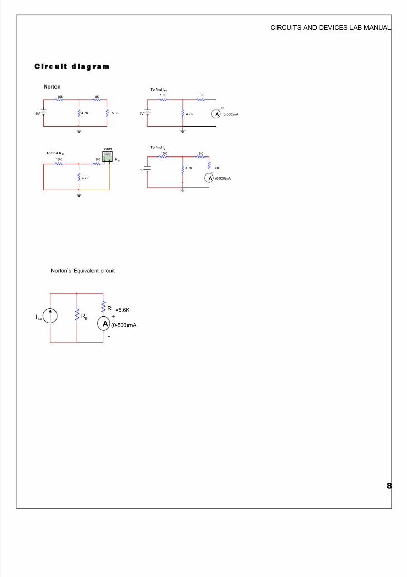
Circuit diagram
5V 5V A+
-(0-500)mA
10K 8K
4.7K 5.6K
10K 8K
4.7K
To find Isc
10K 8K
4.7K
To find R th
XMM1
R th
Isc
5V
10K 8K
4.7K 5.6K
A+
-(0-500)mA
To find IL
Norton
A+
-
(0-500)mA
Isc thR
RL =5.6K
Norton`s Equivalent circuit

5/12/2018 Right Pages of Circuits & Devices Lab Manual for II Sem Ece & Cse - slidepdf.com
http://slidepdf.com/reader/full/right-pages-of-circuits-devices-lab-manual-for-ii-sem-ece-cse 9/36
CIRCUITS AND DEVICES LAB MA
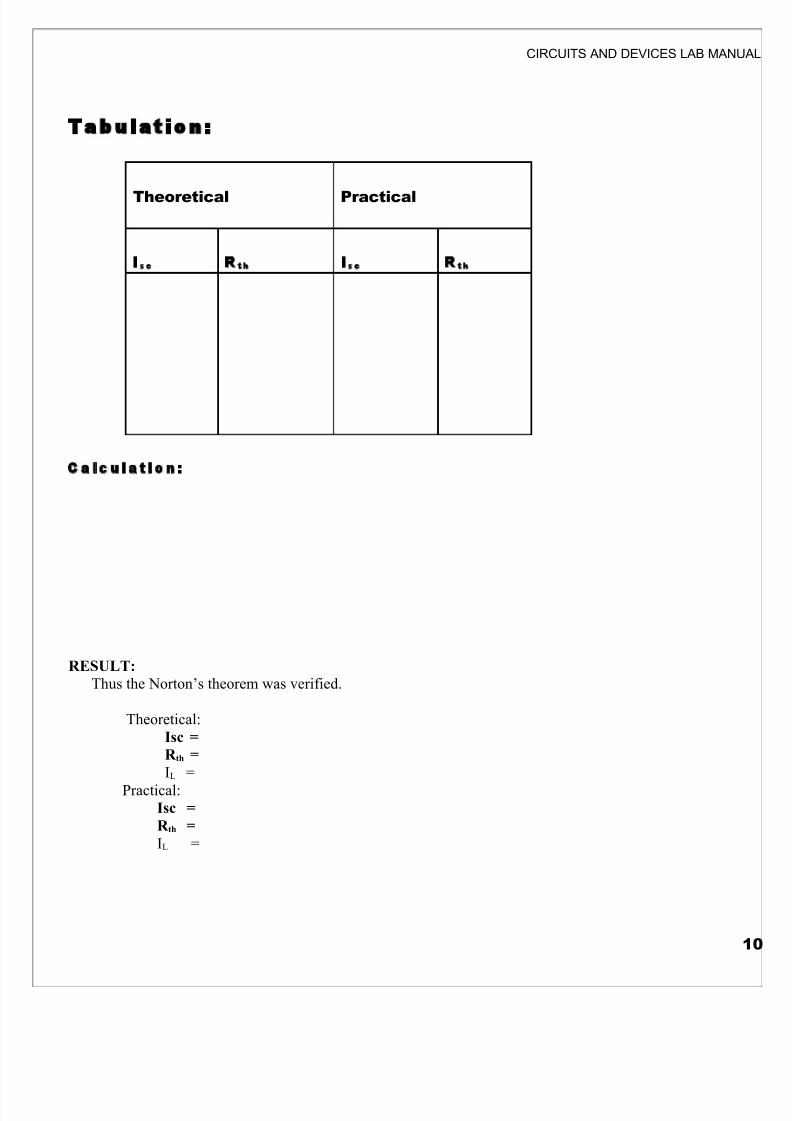
2.b) NORTON’S THEOERM
AIM:
To verify Norton’s theorem and to determine the current flow through the load resistance.
COMPONENTS REQUIRED:
Sl.No components Range Quantity
1
2
3
4
5
RPS
Resistor
Ammeter
Bread board
Connecting wires
(0-15)V
10KΩ,5.6KΩ,8.2K Ω6KΩ
(0-10)mA,mc(0-5)mc,mc
------
------
1
Each 1
11
1
few
Norton’s theorem:
Any linear active network with output terminals can be replaced by a single current source. Isc in pawith a single impedance Zth. Isc is the current through the terminals of the active network when shorted. Zth
called Thevennin`s impedance.
Current through R L= Isc Zth/( Zth+ZL)
PROCEDURE:
1. Connections are made as per the circuit diagram.
2. Check your connections before switch on the supply.3. Find the Norton’s current (or) short circuit current in load resistance.4. Replace voltage source by internal resistor.5. Determine the equivalent’s resistance.6. Find IL by using Norton’s formula.7. Compare the observation reading to theoretical value.8. switch off the supply9. Disconnect the circuit.
5/12/2018 Right Pages of Circuits & Devices Lab Manual for II Sem Ece & Cse - slidepdf.com
http://slidepdf.com/reader/full/right-pages-of-circuits-devices-lab-manual-for-ii-sem-ece-cse 10/36
CIRCUITS AND DEVICES LAB MA
Tabulation:
Theoretical Practical
Isc Rth Isc Rth
Calculation:
RESULT:
Thus the Norton’s theorem was verified.
Theoretical:Isc =
R th =
IL =Practical:
Isc =
R th =
IL =
5/12/2018 Right Pages of Circuits & Devices Lab Manual for II Sem Ece & Cse - slidepdf.com
http://slidepdf.com/reader/full/right-pages-of-circuits-devices-lab-manual-for-ii-sem-ece-cse 11/36
CIRCUITS AND DEVICES LAB MA
Circuit diagram
Superposition
12V 10 V
220 ohm 470 ohm
1 K
10 V
220 ohm 470 ohm
1 K
A+
-(0-20)mA
12V 10 V
220 ohm 470 ohm
1 K
A+
-(0-20)mA
TO find I When 10V source is acting alone2
12V
220 ohm 470 ohm
1 K
A+
-(0-20)mA
To find I when 12V source is acting alone1
To find I when two sources are acting
Tabulation:
V(volt) I1(mA) I2(mA) I(mA)
V
1
V
2
theoretical practical theoretical practical theoretical practica
Calculation:

5/12/2018 Right Pages of Circuits & Devices Lab Manual for II Sem Ece & Cse - slidepdf.com
http://slidepdf.com/reader/full/right-pages-of-circuits-devices-lab-manual-for-ii-sem-ece-cse 12/36
CIRCUITS AND DEVICES LAB MA
3. SUPER POSITION THEOREM
AIM:
To verify superposition theorem and determine the current following through the load resistance. COMPONENTS REQUIRED:
Sl.No components Range Quantity
1
2
3
5
6
RPS
Resistor
Ammeter
Bread board
Connecting wires
(0-15)V
1KΩ,220Ω,470Ω
(0-1)mA,mc
(0-5)mA mc
------
------
1
Each 1
1
1
1
few
Superposition theorem
In a linear circuit containing more than one source, the current that flows at any point or the voltagexists between any two points is the algebraic sum of the currents or the voltages that would have been
produced by each source taken separately with all other sources removed.
PROCEDURE:
1. Connections are made as per the circuit diagram.2. Check your connections before switch on the supply.3. Determine the current through the load resistance.4. Now one of the sources is shorted and the current flowing through the resistance IL measured by
ammeter.5. Similarly, the other source is shorted and the current flowing through the resistance IL measured by
ammeter.6. Compare the value obtained with the sum of I1&I2 should equal to I7. Compare the observation reading to theoretical value.8. switch off the supply9. Disconnect the circuit.
RESULT:
Thus the superposition theorem was verified.

5/12/2018 Right Pages of Circuits & Devices Lab Manual for II Sem Ece & Cse - slidepdf.com
http://slidepdf.com/reader/full/right-pages-of-circuits-devices-lab-manual-for-ii-sem-ece-cse 13/36
CIRCUITS AND DEVICES LAB MA

5/12/2018 Right Pages of Circuits & Devices Lab Manual for II Sem Ece & Cse - slidepdf.com
http://slidepdf.com/reader/full/right-pages-of-circuits-devices-lab-manual-for-ii-sem-ece-cse 14/36
CIRCUITS AND DEVICES LAB MA
4.a) VERIFICATION OF MAXIMUM POWER TRANSFER THEOREM
AIM:
To find the value of resistance R L in which maximum power is transferred to the load resistance.
COMPONENTS REQUIRED:
Sl.No components Range Quantity
1
2
3
4
5
6
Resistor
Ammeter
Bread board
Connecting wires
RPS
DRB
1KΩ,2.2 KΩ
(0-10) mA
-----
------
(0-30)V
(0-10)KΩ
1
1
1
Few
1
1
Maximum power transfer theorem:
Maximum power transfer to the load resistor occurs when it has a value equal to the resistance of the nelooking back at it from the load terminals.
PROCEDURE:
1. Connections are given as per the circuit diagram.2. By giving various values of the resistance in DRB, note the ammeter
reading.3. Calculate the power and plot the power Vs resistance graph.4. Note the maximum power point corresponding resistance from the graph.
RESULT:
Thus the value of unknown resistance in which the maximum power is transferred to the load was fo
Theoretical load resistance =Practical load resistance =Maximum power =
5/12/2018 Right Pages of Circuits & Devices Lab Manual for II Sem Ece & Cse - slidepdf.com
http://slidepdf.com/reader/full/right-pages-of-circuits-devices-lab-manual-for-ii-sem-ece-cse 15/36
CIRCUITS AND DEVICES LAB MA
4.b) VERIFICATION OF RECIPROCITY THEOREM
AIM:
To verify Reciprocity theorem and to determine the current flow through the load resistance.
COMPONENTS REQUIRED:
Sl.No components Range Quantity
1
2
3
4
5
RPS
Resistor
Ammeter
Bread board
Connecting wires
(0-15)V
100Ω,470Ω,820Ω, 100Ω
(0-30) mA,
------
------
1
Each 1
1
1
few
THEORY:
Reciprocity theorem
In a linear, bilateral network a voltage source V volt in a branch gives rise to a current I, in another branch. If V is applied in the second branch the current in the first branch will be I. This V/I are called tran
impedance or resistance. On changing the voltage source from 1 to branch 2, the current in branch 2 appea branch 1.
PROCEDURE:
1. Connect the circuit as per the circuit diagram.2. Switch on the supply and note down the corresponding ammeter readings.3. Find ratio of input voltage to output current.4. Interchange the position of the ammeter and power supply. Note down the
Corresponding ammeter readings
5. Verify the reciprocity theorem by equating the voltage to current ratio.
RESULT:
Thus the reciprocity theorem was verified
5/12/2018 Right Pages of Circuits & Devices Lab Manual for II Sem Ece & Cse - slidepdf.com
http://slidepdf.com/reader/full/right-pages-of-circuits-devices-lab-manual-for-ii-sem-ece-cse 16/36
CIRCUITS AND DEVICES LAB MA
5. a) FREQUENCY RESPONSE OF SERIES RESONANCE CIRCUIT
AIM:
To obtain the resonance frequency of the given RLC series electrical network.
COMPONENTS REQUIRED:
Sl.No components Range Quantity
1
2
3
4
5
6
7
Function generator
Resistor
Voltmeter
capacitor
Bread board
Connecting wires
Decade inductance box
0-2MHz
1KΩ,
(0-5) V
1µF
-----
------
(0-100)mH
1
1
1
1
1
Few
1
FORMULA USED:
Series resonance frequency F=1/ (2п √ (LC))
PROCEDURE:
1. Connections are made as per the circuit diagram.2. Vary the frequency of the function generator from 50 Hz to 20 KHz.3. Measure the corresponding value of voltage across the resistor R for series RLC circuit.4. Repeat the same procedure for different values of frequency.5. Tabulate your observation.6. Note down the resonance frequency from the graph.
RESULT:
Thus the resonance frequency of series RLC circuit is obtained.Practical value =Theoretical value =
5/12/2018 Right Pages of Circuits & Devices Lab Manual for II Sem Ece & Cse - slidepdf.com
http://slidepdf.com/reader/full/right-pages-of-circuits-devices-lab-manual-for-ii-sem-ece-cse 17/36
CIRCUITS AND DEVICES LAB MA
5. b) FREQUENCY RESPONSE OF PARALLEL RESONANCE CIRCUIT
AIM:
To obtain the resonance frequency of the given RLC parallel electrical network.
COMPONENTS REQUIRED:
Sl.No components Range Quantity
1
2
3
4
5
6
7
Function generator
Resistor
Voltmeter
capacitor
Bread board
Connecting wires
Decade inductance box
0-3MHz
1KΩ,
(0-5) V
1µF
-----
------
(0-100)mH
1
1
1
1
1
Few
1
FORMULA USED:
Parallel resonance frequency F=1/ (2п √ (LC)
PROCEDURE:
1. Connections are made as per the circuit diagram.2. Vary the frequency of the function generator from 50 Hz to 20 KHz.3. Measure the corresponding value of voltage across the resistor R for series RLC circuit.4. Repeat the same procedure for different values of frequency.5. Tabulate your observation.6. Note down the resonance frequency from the graph.
RESULT:
Thus the resonance frequency of series RLC circuit is obtained.
Practical value =Theoretical value =
5/12/2018 Right Pages of Circuits & Devices Lab Manual for II Sem Ece & Cse - slidepdf.com
http://slidepdf.com/reader/full/right-pages-of-circuits-devices-lab-manual-for-ii-sem-ece-cse 18/36
CIRCUITS AND DEVICES LAB MA
6. a. CHARACTERISTICS OF PN JUNCTION DIODE
AIM:
To plot the characteristic of PN junction diode.
COMPONENTS REQUIRED:
Sl.No components Range Quantity
1
2
3
4
5
6
7
Diode
RPS
Resistor
Ammeter
voltmeter
Bread board
Connecting wires
IN 4001
(0-30)V
1KΩ,
(0-50)mA(0-500)µA
(0-1)V(0-30)V
----
------
1
1
1
11
111
few
FORMULA USED:
1. Forward Resistance R f =ΔVF/ΔIF
2. Reverse Resistance R r = ΔVR /ΔIR
PROCEDURE:
Forward bias:
1. The circuit connections are made as per the circuit diagram2. Vary the power supply voltage such a way that readings are taken in steps of .1 V in the voltmeter.3. Note down the corresponding ammeter readings.4. Plot the graph current Vs voltage.5. calculate dynamic resistance r=(V/I)
Reverse bias:
1. Connect the circuit as per the circuit diagram.2. Vary the power supply in step by 1 V.3. Note down corresponding ammeter reading.4. Plot the graph current Vs voltage.
RESULT:
Thus the characteristic of PN junction diode was obtained.
5/12/2018 Right Pages of Circuits & Devices Lab Manual for II Sem Ece & Cse - slidepdf.com
http://slidepdf.com/reader/full/right-pages-of-circuits-devices-lab-manual-for-ii-sem-ece-cse 19/36
CIRCUITS AND DEVICES LAB MA
(i)Forward resistance= (ii)Reverse resistance=6.b) CHARACTERISTICS OF ZENER DIODE
AIM:
To draw the V-I characteristic of Zener diode and find the parameter.
COMPONENTS REQUIRED:
Sl.No components Range Quantity
1
2
3
4
5
6
7
Zener Diode
RPS
Resistor
Ammeter
voltmeter
Bread board
Connecting wires
(0-30)V
1KΩ,
(0-50)mA
(0-1)V
----
------
1
1
1
1
1
1
few
FORMULA USED:
1. Forward Resistance R f =ΔVF/ΔIF
2. Reverse Resistance R r = ΔVR /ΔIR
PROCEDURE:
Forward bias characteristic:
1. The circuit connections are made as per the circuit diagram2. Keep the RPS connected in a minimum value and switch ON the power supply gradually increase
voltage in step of .1V .3. Note down the corresponding ammeter and voltmeter readings.
4. Plot the forward V-I curve .5. calculate forward resistance R f =(V/I)

5/12/2018 Right Pages of Circuits & Devices Lab Manual for II Sem Ece & Cse - slidepdf.com
http://slidepdf.com/reader/full/right-pages-of-circuits-devices-lab-manual-for-ii-sem-ece-cse 20/36
CIRCUITS AND DEVICES LAB MA
Reverse bias characteristic:
1. Connect the circuit as per the circuit diagram.2. Keep the RPS connected in a minimum value and switch ON the power supply.3. Gradually increase voltage in step of .1V.
4. Vary the power supply in step by 1 V.5. Note down corresponding reverse voltage and current.6. Plot the graph current Vs voltage.7. Plot the reverse V-I curve.
RESULT:Thus the characteristic of Zener diode was studied and their characteristic was drawn.
(i)Forward resistance=
5/12/2018 Right Pages of Circuits & Devices Lab Manual for II Sem Ece & Cse - slidepdf.com
http://slidepdf.com/reader/full/right-pages-of-circuits-devices-lab-manual-for-ii-sem-ece-cse 21/36
CIRCUITS AND DEVICES LAB MA
(ii)Reverse resistance=
7. CHARACTERISTICS OF CE CONFIGURATION
AIM:
To draw input and output characteristics of BJT in CE configuration and to determine its parameter.
COMPONENTS REQUIRED:
Sl.No components Range Quantity
1
2
3
4
5
6
7
Transistor
RPS
Resistor
Ammeter
voltmeter
Bread board
Connecting wires
Bc 547
(0-30)V
1KΩ,
(0-50)mA(0-500) µA
(0-1)V,mc(0-30)V,mc
----
------
1
2
2
1
11
1
few
FORMULA USED:
1. Input impedance (hie) =ΔVBE/ΔIB at VCE constant2. Forward current gain (hfe) = ΔIC/ΔIB at VCE constant3. Output conductance (hoe) = ΔIC/ΔVCE at IB constant4. Reverse voltage gain (hre) = ΔVBE/ΔVCE at IB constant
PROCEDURE:
1. The circuit connections are made as per the circuit diagram2. To draw the input characteristics VCE is kept constant3. Input RPS is varied and the corresponding values of IB and VBE
Voltage are noted4. To draw the output characteristics IB is kept constant5. output RPS is varied and the corresponding values of IC and VCE are
Noted.

5/12/2018 Right Pages of Circuits & Devices Lab Manual for II Sem Ece & Cse - slidepdf.com
http://slidepdf.com/reader/full/right-pages-of-circuits-devices-lab-manual-for-ii-sem-ece-cse 22/36
CIRCUITS AND DEVICES LAB MA
6. Corresponding input and output characteristics curves are drawn.
RESULT:
Thus the static characteristics of CE mode configuration is drawn from the output graph the h -
parameter are determined.(i)Input impedance=
(ii)Forward current gain=
(iii)Output conductance=
(iv)Reverse voltage gain=
5/12/2018 Right Pages of Circuits & Devices Lab Manual for II Sem Ece & Cse - slidepdf.com
http://slidepdf.com/reader/full/right-pages-of-circuits-devices-lab-manual-for-ii-sem-ece-cse 23/36
CIRCUITS AND DEVICES LAB MA
8. STATIC CHARACTERISTICS OF CB CONFIGURATION
AIM:
To draw input and output characteristics of BJT in CB configuration and to determine its parameter.
COMPONENTS REQUIRED:
Sl.No components Range Quantity
1
2
3
4
5
6
7
Transistor
RPS
Resistor
Ammeter
voltmeter
Bread board
Connecting wires
BC 547
(0-30)V
1KΩ,
(0-30)mA(0-30) mA
(0-2)V,mc(0-30)V,mc
----
------
1
2
2
11
111
Few
FORMULAS USED:
1. Input impedance (hie) =ΔVBE/ΔIE at VCB constant2. Forward current gain (hfe) = ΔIC/ΔIE at VCB constant3. Output conductance (hoe) = ΔIC/ΔVCB at IE constant4. Reverse voltage gain (hre) = ΔVBE/ΔVCB at IE constant
PROCEDURE:
1. The circuit connections are made as per the circuit diagram2. To draw the input characteristics VCB is kept constant3. VBE is varied and the corresponding values of IE are noted4. To draw the output characteristics IE is kept constant5. VCB is varied and the corresponding values of IC are noted6. Corresponding input and output characteristics curves are drawn
5/12/2018 Right Pages of Circuits & Devices Lab Manual for II Sem Ece & Cse - slidepdf.com
http://slidepdf.com/reader/full/right-pages-of-circuits-devices-lab-manual-for-ii-sem-ece-cse 24/36
CIRCUITS AND DEVICES LAB MA
RESULT:
Thus the static characteristics of transistor under the CB mode
Was determined.
(i)Input impedance (hib) =
(ii)Forward current gain (hfb) =
(iii)Output conductance (hob) =
5/12/2018 Right Pages of Circuits & Devices Lab Manual for II Sem Ece & Cse - slidepdf.com
http://slidepdf.com/reader/full/right-pages-of-circuits-devices-lab-manual-for-ii-sem-ece-cse 25/36
CIRCUITS AND DEVICES LAB MA
(iv)Reverse voltage gain (hrb) =
9.a) CHARACTERISTICS OF UJT
AIM: To determine the static characteristics of UJT.
COMPONENTS REQUIRED:
Sl.No components Range Quantity
1
2
3
4
5
6
7
UJT
RPS
Resistor
Ammeter
voltmeter
Bread board
Connecting wires
2N2646
(0-30)V
1KΩ,22KΩ
(0-50)mA
(0-10)V,mc(0-30)V,mc
----
------
1
2
Each 1
1
111
Few
FORMULA USED:
1. Negative resistance = ∆VBE/∆IE.
2. Intrinsic stand off ratio = (VP-VBE)/VB1B2.
PROCEDURE:
1. Circuit connections are made as per the circuit diagram.2. The voltage VB1B2 is kept constant and VBE is varied.
3. The corresponding values of IE are noted.4. For different constant values of VB1B2 the values of VBE & IE are noted.5. The input side RPS is varied slowly from zero and the voltmeter readings
are noted.6. At one point, the needle deflects back and currents starts increasing.7. The currents must not increase beyond 25mA.8. Graph is plotted.9. The current must not increase beyond .25mA.
5/12/2018 Right Pages of Circuits & Devices Lab Manual for II Sem Ece & Cse - slidepdf.com
http://slidepdf.com/reader/full/right-pages-of-circuits-devices-lab-manual-for-ii-sem-ece-cse 26/36
CIRCUITS AND DEVICES LAB MA
APPLICATION:
1. Square or Saw tooth wave generator.2. over voltage detector.
3. Switching, timing phase control circuit etc.
RESULT:
Thus the parameter of UJT was determined from its characteristics.
1. negative resistance =2. intrinsic stand off ratio =
5/12/2018 Right Pages of Circuits & Devices Lab Manual for II Sem Ece & Cse - slidepdf.com
http://slidepdf.com/reader/full/right-pages-of-circuits-devices-lab-manual-for-ii-sem-ece-cse 27/36
CIRCUITS AND DEVICES LAB MA
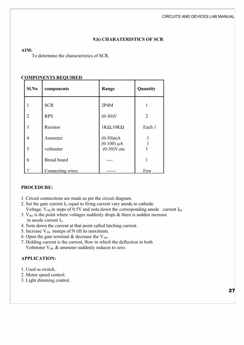
9.b) CHARATERISTICS OF SCR
AIM:
To determine the characteristics of SCR.
COMPONENTS REQUIRED:
Sl.No components Range Quantity
1
2
3
4
5
6
7
SCR
RPS
Resistor
Ammeter
voltmeter
Bread board
Connecting wires
2P4M
(0-30)V
1KΩ,10KΩ
(0-50)mA(0-100) μA(0-30)V,mc
----
------
1
2
Each 1
111
1
Few
PROCEDURE:
1. Circuit connections are made as per the circuit diagram.2. Set the gate current IG equal to firing current vary anode to cathode
Voltage, VAK in steps of 0.5V and note down the corresponding anode current IAK
3. VBO is the point where voltages suddenly drops & there is sudden increasein anode current IA.
4. Note down the current at that point called latching current.5. Increase VAK insteps of N till its maximum.6. Open the gate terminal & decrease the VAK .
7. Holding current is the current, flow in which the deflection in bothVoltmeter VAK & ammeter suddenly reduces to zero.
APPLICATION:
1. Used as switch..2. Motor speed control.3. Light dimming control.

5/12/2018 Right Pages of Circuits & Devices Lab Manual for II Sem Ece & Cse - slidepdf.com
http://slidepdf.com/reader/full/right-pages-of-circuits-devices-lab-manual-for-ii-sem-ece-cse 28/36
CIRCUITS AND DEVICES LAB MA
4. Phase control
RESULT:
Thus the characteristic of SCR was determined.Latching current =Holding current =VBO current =
5/12/2018 Right Pages of Circuits & Devices Lab Manual for II Sem Ece & Cse - slidepdf.com
http://slidepdf.com/reader/full/right-pages-of-circuits-devices-lab-manual-for-ii-sem-ece-cse 29/36
CIRCUITS AND DEVICES LAB MA
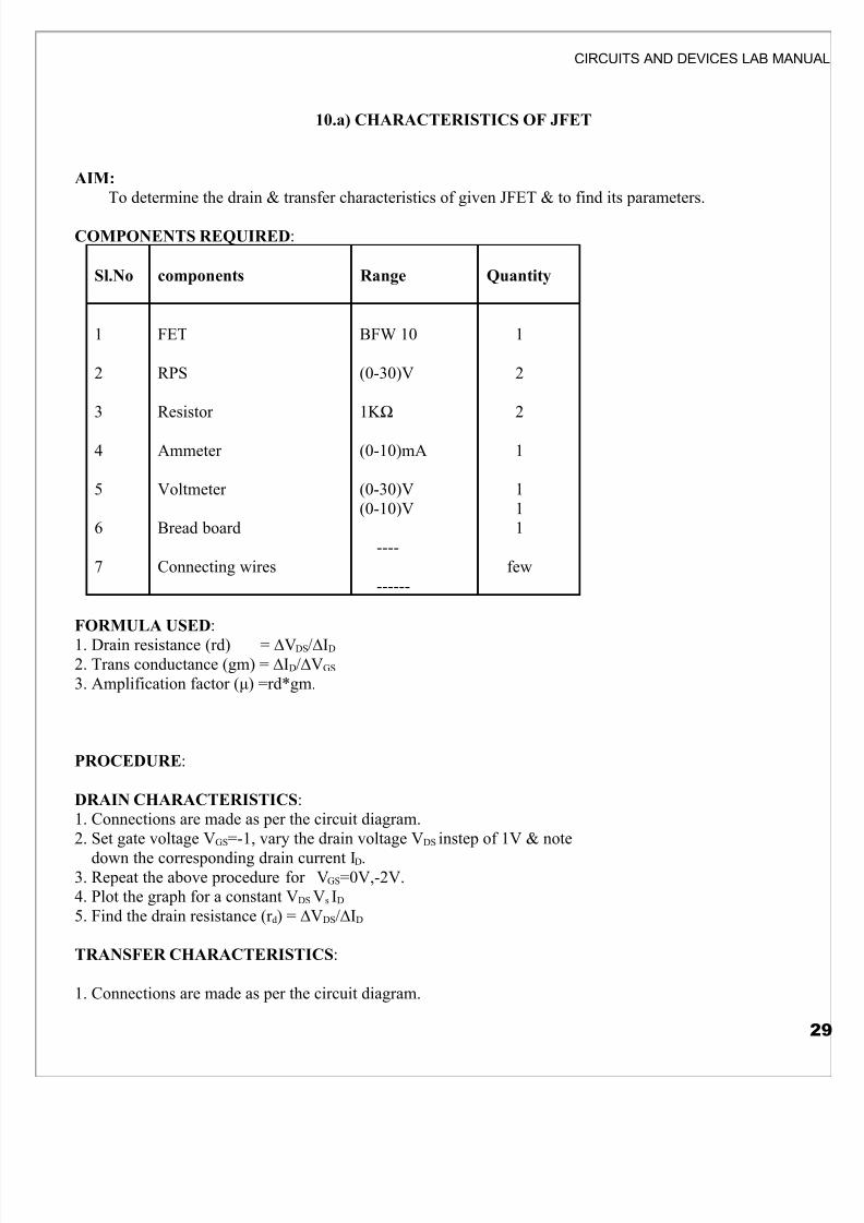
10.a) CHARACTERISTICS OF JFET
AIM:
To determine the drain & transfer characteristics of given JFET & to find its parameters.
COMPONENTS REQUIRED:
Sl.No components Range Quantity
1
2
3
4
5
6
7
FET
RPS
Resistor
Ammeter
Voltmeter
Bread board
Connecting wires
BFW 10
(0-30)V
1KΩ
(0-10)mA
(0-30)V(0-10)V
----
------
1
2
2
1
111
few
FORMULA USED:
1. Drain resistance (rd) = ∆VDS/∆ID
2. Trans conductance (gm) = ∆ID/∆VGS
3. Amplification factor (μ) =rd*gm.
PROCEDURE:
DRAIN CHARACTERISTICS:
1. Connections are made as per the circuit diagram.2. Set gate voltage VGS=-1, vary the drain voltage VDS instep of 1V & note
down the corresponding drain current ID.3. Repeat the above procedure for VGS=0V,-2V.4. Plot the graph for a constant VDS Vs ID
5. Find the drain resistance (r d) = ∆VDS/∆ID
TRANSFER CHARACTERISTICS:
1. Connections are made as per the circuit diagram.
5/12/2018 Right Pages of Circuits & Devices Lab Manual for II Sem Ece & Cse - slidepdf.com
http://slidepdf.com/reader/full/right-pages-of-circuits-devices-lab-manual-for-ii-sem-ece-cse 30/36
CIRCUITS AND DEVICES LAB MA
2. Set gate voltage VDS=1V, vary the gate voltage VGS in step of 1V andnote down the corresponding drain current ID
3. Repeat the above procedure for VDS=5V, 10V.4. Plot the graph for VGS Vs ID.
5. Find the Trans conductance (gm)gm = ∆ID/∆VGS
APPLICATION:
1. Used as a buffer in measuring instruments.2. Used as a voltage variable resistor.3. Used in oscillator circuits.4. Used in cascade amplifier.
RESULT:
Thus the drain and transfer characteristics of JFET is drawn and the parameters were determined.
1. Drain resistance (r d) =…………2. Trans conductance (gm) =…………
5/12/2018 Right Pages of Circuits & Devices Lab Manual for II Sem Ece & Cse - slidepdf.com
http://slidepdf.com/reader/full/right-pages-of-circuits-devices-lab-manual-for-ii-sem-ece-cse 31/36
CIRCUITS AND DEVICES LAB MA
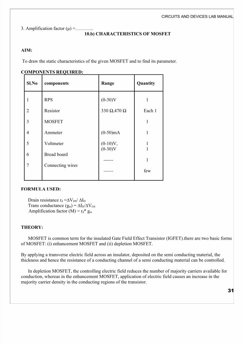
3. Amplification factor (μ) =………...10.b) CHARACTERISTICS OF MOSFET
AIM:
To draw the static characteristics of the given MOSFET and to find its parameter.
COMPONENTS REQUIRED:
Sl.No components Range Quantity
1
2
3
4
5
6
7
RPS
Resistor
MOSFET
Ammeter
Voltmeter
Bread board
Connecting wires
(0-30)V
330 Ω,470 Ω
(0-50)mA
(0-10)V,(0-30)V
------
------
1
Each 1
1
1
11
1
few
FORMULA USED:
Drain resistance r d =∆VDS/ ∆ID
Trans conductance (gm) = ∆ID/∆VGS
Amplification factor (M) = r d* gm
THEORY:
MOSFET is common term for the insulated Gate Field Effect Transistor (IGFET).there are two basic fof MOSFET: (i) enhancement MOSFET and (ii) depletion MOSFET.
By applying a transverse electric field across an insulator, deposited on the semi conducting material, thethickness and hence the resistance of a conducting channel of a semi conducting material can be controlled
In depletion MOSFET, the controlling electric field reduces the number of majority carriers available conduction, whereas in the enhancement MOSFET, application of electric field causes an increase in themajority carrier density in the conducting regions of the transistor.
5/12/2018 Right Pages of Circuits & Devices Lab Manual for II Sem Ece & Cse - slidepdf.com
http://slidepdf.com/reader/full/right-pages-of-circuits-devices-lab-manual-for-ii-sem-ece-cse 32/36
CIRCUITS AND DEVICES LAB MA
PROCEDURE:
Transfer characteristics:1. Connections are made as per the circuit diagram.2. Set VDS some constant voltage.3. vary the input side RPS measure the corresponding VGS and ID
4. measure the VGS in which ammeter shows deflection and VDS
5. Plot the graph voltage against current. Drain characteristics:
1. Set the input above the threshold voltage.2. Vary the input side RPS and measure the corresponding VDS and ID
3. Plot the graph voltage against current.
RESULT:
Thus the characteristics of MOSFET were drawn.
Drain resistance r d =∆VDS/ ∆ID=
Trans conductance (gm)= ∆ID/∆VGS =
Amplification factor (M) = r d* gm=11. a) CHARACTERISTICS OF DIAC
5/12/2018 Right Pages of Circuits & Devices Lab Manual for II Sem Ece & Cse - slidepdf.com
http://slidepdf.com/reader/full/right-pages-of-circuits-devices-lab-manual-for-ii-sem-ece-cse 33/36
CIRCUITS AND DEVICES LAB MA
AIM:
To draw the VI characteristics of the given DIAC and determine cut in voltage.
COMPONENTS REQUIRED:
Sl.No components Range Quantity
1
2
3
4
5
6
7
RPS
Resistor
DIAC
Ammeter
Voltmeter
Bread board
Connecting wires
(0-60)V
1 KΩ
DB3
(0-30)mA
(0-50)V
------
------
1
1
1
1
1
1
few
THEORY:
DIAC is a three layer and two terminal semiconductor devices. MT1and MT2 is the two main terminalwhich are interchangeable. It acts as a bidirectional avalanche diode. It does not have any control terminalhas two junctions J1 and J2. Though the diac resembles a bipolar transistor, the central layer is free from aconnection with the terminals.
DIAC CHARACTERISTICS:It acts as a switch in both directions. As the doping level at the two ends of the device is the same, th
Diac has identical characteristics for both positive and negative half of an a.c cycle. During the positive hacycle, MT1 is positive with respect to MT2 whereas MT2 is positive with respect to MT1 in the negative halcycle. At the voltage less than the break over voltage, a very small amount of current called the leakage cuflows through the device and the device remains in off state. When the voltage level reaches the break ovevoltage, the device starts conducting and it exhibits negative resistance characteristics ,i.e. the current flowthe device starts increasing and the voltage across it starts decreasing.
5/12/2018 Right Pages of Circuits & Devices Lab Manual for II Sem Ece & Cse - slidepdf.com
http://slidepdf.com/reader/full/right-pages-of-circuits-devices-lab-manual-for-ii-sem-ece-cse 34/36
CIRCUITS AND DEVICES LAB MA
PROCEDURE:
1. MT1 is positive w.r.t MT2.2. Connections are made as per the circuit diagram.3. Vary the power supply.4. Note down the corresponding ammeter and voltmeter reading.5. Plot the graph V against I.6. MT1 is negative w.r.t. MT2.7. Repeat the step 3 to 5.
RESULT:
Thus the characteristics of DIAC were drawn and the cut in voltage was determined
11.b) CHARACTERISTICS OF TRIAC
5/12/2018 Right Pages of Circuits & Devices Lab Manual for II Sem Ece & Cse - slidepdf.com
http://slidepdf.com/reader/full/right-pages-of-circuits-devices-lab-manual-for-ii-sem-ece-cse 35/36
CIRCUITS AND DEVICES LAB MA
AIM:
To draw the characteristics of the given TRIAC and determine break over voltage.
COMPONENTS REQUIRED:
Sl.No components Range Quantity
1
2
3
4
5
6
7
RPS
Resistor
TRIAC
Ammeter
Voltmeter
Bread board
Connecting wires
(0-30)V
1 KΩ/5w, 1 KΩ
(0-50)mA
(0-15)V(0-30)V
------
------
2
2
1
2
111
few
THEORY:
It is a three terminal semiconductor switching device which can control alternating current in a loathree terminals are MT1 and MT2 and the gate. Triac is equivalent to two SCRs connected in parallel but ireverse direction. So triac will act as a switch for both directions.
Like an SCR, a triac also starts conducting only when the breakover voltage is reached. Earlier to the leakage current which is very small in magnitude flows through the device and therefore remains in thstate. The device, when starts conducting, allows very heavy amount of current to flow through it. The higinrush of current must be limited using external resistance, or it may otherwise damage the device.
During the positive half cycle, MT1 is positive w.r.t MT2, whereas MT2 is positive w.r.t MT1 duringnegative half cycle. A Triac is a bidirectional device and can be triggered either by a positive or by a negagate signal. By applying proper signal at the gate, the breakover voltage of the device can be changed: thu phase control process can be achieved.
Triac is used for illumination control, temperature control, liquid level control, motor speed controas static switch to turn a.c power ON and OFF.
5/12/2018 Right Pages of Circuits & Devices Lab Manual for II Sem Ece & Cse - slidepdf.com
http://slidepdf.com/reader/full/right-pages-of-circuits-devices-lab-manual-for-ii-sem-ece-cse 36/36
CIRCUITS AND DEVICES LAB MA
PROCEDURE:
1. Connect the circuit as per circuit diagram.2. To set gate current (Ig),VMT1,VMT2
3. Vary Vg till VAK suddenly drops.
4. Note down the corresponding IG,set gate current equal firing current.5. Vary anode to cathode Vge.6. Vary VAK supply voltage in steps 7 note down the corresponding ammeter readings.
7. Open the gate terminal & decrease VAK.
RESULT:
Thus the characteristic of TRIAC was drawn.
MT1 break over voltage (VBO) =MT1 break over current (IBO) =MT2 break over voltage (-VBO) =MT2 break over current (-IBO) =