rf and microwave transistor oscillator design...practising rf designers and engineers, as an...
TRANSCRIPT

JWBK153-FM JWBK153-Grebennikov March 13, 2007 23:46
RF and Microwave
Transistor Oscillator Design
i

JWBK153-FM JWBK153-Grebennikov March 13, 2007 23:46
ii

JWBK153-FM JWBK153-Grebennikov March 13, 2007 23:46
RF and Microwave
Transistor Oscillator Design
Andrei Grebennikov
Infineon Technologies AG, Germany
iii

JWBK153-FM JWBK153-Grebennikov March 13, 2007 23:46
Copyright C© 2007 John Wiley & Sons Ltd, The Atrium, Southern Gate, Chichester,West Sussex PO19 8SQ, England
Telephone (+44) 1243 779777
Email (for orders and customer service enquiries): [email protected] our Home Page on www.wiley.com
All Rights Reserved. No part of this publication may be reproduced, stored in a retrieval system ortransmitted in any form or by any means, electronic, mechanical, photocopying, recording, scanning orotherwise, except under the terms of the Copyright, Designs and Patents Act 1988 or under the termsof a licence issued by the Copyright Licensing Agency Ltd, 90 Tottenham Court Road, LondonW1T 4LP, UK, without the permission in writing of the Publisher. Requests to the Publisher should beaddressed to the Permissions Department, John Wiley & Sons Ltd, The Atrium, Southern Gate,Chichester, West Sussex PO19 8SQ, England, or emailed to [email protected], or faxed to(+44) 1243 770620.
Designations used by companies to distinguish their products are often claimed as trademarks. All brandnames and product names used in this book are trade names, service marks, trademarks or registeredtrademarks of their respective owners. The Publisher is not associated with any product or vendormentioned in this book.
This publication is designed to provide accurate and authoritative information in regard to the subjectmatter covered. It is sold on the understanding that the Publisher is not engaged in renderingprofessional services. If professional advice or other expert assistance is required, the services of acompetent professional should be sought.
Other Wiley Editorial Offices
John Wiley & Sons Inc., 111 River Street, Hoboken, NJ 07030, USA
Jossey-Bass, 989 Market Street, San Francisco, CA 94103-1741, USA
Wiley-VCH Verlag GmbH, Boschstr. 12, D-69469 Weinheim, Germany
John Wiley & Sons Australia Ltd, 42 McDougall Street, Milton, Queensland 4064, Australia
John Wiley & Sons (Asia) Pte Ltd, 2 Clementi Loop #02-01, Jin Xing Distripark, Singapore 129809
John Wiley & Sons Canada Ltd, 6045 Freemont Blvd, Mississauga, ONT, Canada L5R 4J3
Wiley also publishes its books in a variety of electronic formats. Some content that appears inprint may not be available in electronic books.
Anniversary Logo Design: Richard J. Pacifico
British Library Cataloguing in Publication Data
A catalogue record for this book is available from the British Library
ISBN 978-0-470-02535-2 (HB)
Typeset in 10/12pt Times Roman by TechBooks, New Delhi, India.Printed and bound in Great Britain by Antony Rowe Ltd, Chippenham, WiltshireThis book is printed on acid-free paper responsibly manufactured from sustainable forestryin which at least two trees are planted for each one used for paper production.
iv
JWBK153-FM JWBK153-Grebennikov March 13, 2007 23:46
Contents
About the Author ix
Preface xi
Acknowledgements xv
1 Nonlinear circuit design methods 11.1 Spectral-domain analysis 1
1.1.1 Trigonometric identities 21.1.2 Piecewise-linear approximation 41.1.3 Bessel functions 8
1.2 Time-domain analysis 91.3 Newton–Raphson algorithm 121.4 Quasilinear method 151.5 Van der Pol method 201.6 Computer-aided analysis and design 24
References 28
2 Oscillator operation and design principles 292.1 Steady-state operation mode 292.2 Start-up conditions 312.3 Oscillator configurations and historical aspects 362.4 Self-bias condition 432.5 Oscillator analysis using matrix techniques 50
2.5.1 Parallel feedback oscillator 502.5.2 Series feedback oscillator 53
2.6 Dual transistor oscillators 552.7 Transmission-line oscillator 602.8 Push–push oscillator 652.9 Triple-push oscillator 722.10 Oscillator with delay line 75
References 79
v

JWBK153-FM JWBK153-Grebennikov March 13, 2007 23:46
vi CONTENTS
3 Stability of self-oscillations 833.1 Negative-resistance oscillator circuits 833.2 General single-frequency stability condition 863.3 Single-resonant circuit oscillators 87
3.3.1 Series resonant circuit oscillator with constant load 873.3.2 Parallel resonant circuit oscillator with nonlinear load 88
3.4 Double-resonant circuit oscillator 893.5 Stability of multi-resonant circuits 91
3.5.1 General multi-frequency stability criterion 913.5.2 Two-frequency oscillation mode and its stability 933.5.3 Single-frequency stability of oscillator with two coupled
resonant circuits 943.5.4 Transistor oscillators with two coupled resonant circuits 96
3.6 Phase plane method 1053.6.1 Free-running oscillations in lossless resonant LC circuits 1063.6.2 Oscillations in lossy resonant LC circuits 1083.6.3 Aperiodic process in lossy resonant LC circuits 1103.6.4 Transformer-coupled MOSFET oscillator 112
3.7 Nyquist stability criterion 1133.8 Start-up and stability 118
References 125
4 Optimum design and circuit technique 1274.1 Empirical optimum design approach 1284.2 Analytic optimum design approach 1364.3 Parallel feedback oscillators 138
4.3.1 Optimum oscillation condition 1384.3.2 Optimum MOSFET oscillator 139
4.4 Series feedback bipolar oscillators 1424.4.1 Optimum oscillation condition 1424.4.2 Optimum common base oscillator 1434.4.3 Quasilinear approach 1464.4.4 Computer-aided design 150
4.5 Series feedback MESFET oscillators 1524.5.1 Optimum common gate oscillator 1524.5.2 Quasilinear approach 1544.5.3 Computer-aided design 157
4.6 High-efficiency design technique 1624.6.1 Class C operation mode 1624.6.2 Class E power oscillators 1654.6.3 Class DE power oscillators 1704.6.4 Class F mode and harmonic tuning 172
4.7 Practical oscillator schematics 177References 182
JWBK153-FM JWBK153-Grebennikov March 13, 2007 23:46
CONTENTS vii
5 Noise in oscillators 1875.1 Noise figure 1875.2 Flicker noise 1965.3 Active device noise modelling 198
5.3.1 MOSFET devices 1985.3.2 MESFET devices 2005.3.3 Bipolar transistors 203
5.4 Oscillator noise spectrum: linear model 2055.4.1 Parallel feedback oscillator 2055.4.2 Negative resistance oscillator 2145.4.3 Colpitts oscillator 216
5.5 Oscillator noise spectrum: nonlinear model 2195.5.1 Kurokawa approach 2195.5.2 Impulse response model 224
5.6 Loaded quality factor 2355.7 Amplitude-to-phase conversion 2395.8 Oscillator pulling figure 241
References 245
6 Varactor and oscillator frequency tuning 2516.1 Varactor modelling 2516.2 Varactor nonlinearity 2556.3 Frequency modulation 2586.4 Anti-series varactor pair 2626.5 Tuning linearity 267
6.5.1 VCOs with lumped elements 2676.5.2 VCOs with transmission lines 273
6.6 Reactance compensation technique 2766.7 Practical VCO schematics 280
6.7.1 VCO implementation techniques 2806.7.2 Differential VCOs 2866.7.3 Push–push VCOs 292
References 296
7 CMOS voltage-controlled oscillators 2997.1 MOS varactor 2997.2 Phase noise 3057.3 Flicker noise 3107.4 Tank inductor 3137.5 Circuit design concepts and technique 317
7.5.1 Device operation modes 3177.5.2 Start-up and steady-state conditions 3217.5.3 Differential cross-coupled oscillators 3257.5.4 Wideband tuning techniques 3267.5.5 Quadrature VCOs 331

JWBK153-FM JWBK153-Grebennikov March 13, 2007 23:46
viii CONTENTS
7.6 Implementation technology issues 3337.7 Practical schematics of CMOS VCOs 335
References 342
8 Wideband voltage-controlled oscillators 3478.1 Main requirements 3478.2 Single-resonant circuits with lumped elements 351
8.2.1 Series resonant circuit 3518.2.2 Parallel resonant circuit 353
8.3 Double-resonant circuit with lumped elements 3568.4 Transmission line circuit realization 360
8.4.1 Oscillation system with uniform transmission line 3608.4.2 Oscillation system with multi-section transmission line 365
8.5 VCO circuit design aspects 3698.5.1 Common gate MOSFET and MESFET VCOs 3698.5.2 Common collector bipolar VCO 3738.5.3 Common base bipolar VCO 376
8.6 Wideband nonlinear design 3788.7 Dual mode varactor tuning 3818.8 Practical RF and microwave wideband VCOs 387
8.8.1 Wireless and satellite TV applications 3878.8.2 Microwave monolithic VCO design 3918.8.3 Push–push oscillators and oscipliers 394
References 396
9 Noise reduction techniques 3999.1 Resonant circuit design technique 399
9.1.1 Oscillation systems with lumped elements 4009.1.2 Oscillation systems with transmission lines 402
9.2 Low-frequency loading and feedback optimization 4109.3 Filtering technique 4169.4 Noise-shifting technique 4239.5 Impedance noise matching 4269.6 Nonlinear feedback loop noise suppression 430
References 433
Index 437

JWBK153-FM JWBK153-Grebennikov March 13, 2007 23:46
About the Author
Dr Andrei Grebennikov, IEEE Senior Member, has obtained long-term academic and indus-trial experience. He worked with Moscow Technical University of Telecommunications andInformatics, Russia; Institute of Microelectronics, Singapore; M/A-COM, Ireland and InfineonTechnologies, Germany, as an engineer, researcher, lecturer and educator.
Dr Grebennikov has lectured as a Guest Professor in University of Linz, Austria, and presentedshort courses as an Invited Speaker at the International Microwave Symposium, EuropeanMicrowave Conference and Motorola Design Centre, Malaysia. He is also the author of morethan 60 papers, 3 books and several US patents.
ix

JWBK153-FM JWBK153-Grebennikov March 13, 2007 23:46
x

JWBK153-FM JWBK153-Grebennikov March 13, 2007 23:46
Preface
The main objective of this book is to present all relevant information necessary for RF andmicrowave transistor oscillator design including well-known and new theoretical approachesand practical circuit schematics and designs, as well as to suggest optimum design approaches,which combine effectively analytic calculations and computer-aided design. This book canbe useful for lecturing to promote the analytical way of thinking and combine effectivelytheory and practice of RF and microwave engineering. As often happens, a new result is along-forgotten old one. Therefore, not only new results based on new technologies or circuitschematics are given, but some old ideas, schematics or approaches are also introduced, thatcould be very useful in modern practice or could contribute to the development of new ideasor techniques.
As a result, this book is intended for and can be recommended to:� university-level professors and researchers, as possible reference and well-founded materialfor creative research and teaching activity which will contribute to strong background forgraduates and postgraduates students;� R&D staff, to combine the theoretical analysis and practical aspects, including computer-aided design (CAD) and to provide a sufficient basis for new ideas in theory and practicalcircuit techniques;� practising RF designers and engineers, as an anthology of many well-known and new prac-tical transistor oscillator circuits with detailed descriptions of their operational principlesand applications and clear practical demonstration of theoretical results.
Chapter 1 presents the most commonly used design techniques for analysing nonlinear cir-cuits, in particular, transistor oscillators. There are several approaches to analyse and designnonlinear circuits, depending on their main specifications. That means an analysis both inthe time domain to determine transient circuit behaviour and in the frequency domain toimprove power and spectral performances when parasitic effects such as instability and spuriousemission must be eliminated or minimized. Using the time-domain technique, it is relativelyeasy to describe a nonlinear circuit with differential equations, which can be solved analyticallyin explicit form for only some simple cases. Under the assumption of slowly varying amplitudeand phase, it is possible to obtain the separate truncated first-order differential equations forthe amplitude and phase of the oscillation process from the original second-order nonlineardifferential equation. However, generally it is necessary to use numerical methods. The time-domain analysis is limited to its inability to operate with the circuit immittance (impedance or
xi

JWBK153-FM JWBK153-Grebennikov March 13, 2007 23:46
xii PREFACE
admittance) parameters as well as the fact that it can be practically applied only for circuitswith lumped parameters or ideal transmission lines. The frequency-domain analysis is lessambiguous because a relatively complex circuit can often be reduced to one or more sets ofimmittances at each harmonic component. For example, using a quasilinear approach, thenonlinear circuit parameters averaged by the fundamental component allow one to apply alinear circuit analysis. Advanced modern CAD simulators incorporate both time-domain andfrequency-domain methods as well as optimization techniques to provide all the necessarydesign cycles.
Chapter 2 introduces the principles of oscillator design, including start-up and steady-state operation conditions, basic oscillator configurations using lumped and transmission-lineelements and simplified equation-based oscillator analysis and design techniques. An immit-tance design approach is introduced and applied to series and parallel feedback oscillators,including circuit design and simulation aspects. Numerous practical examples of RF and mi-crowave oscillators using MOSFET, MESFET and bipolar devices, including the descriptionsof their circuit realizations, are given.
Applying dc bias to the active device does not generally result in the negative resistancecondition. This condition has to be induced in these devices and it is determined by the physicalmechanism in the device and chosen circuit topology. The transistor in the oscillator circuitsis mostly represented as the active two-port network, whose operation principle is reflectedthrough its equivalent circuit. The influence of the circuit and transistor parameters can resultin a hysteresis effect or oscillation instability in practical design. In high-frequency practicalimplementation, the presence of the parasitic device and circuit elements can contribute to themulti-resonant circuits. The possibility of an operation mode with different natural frequen-cies depends on the value of the coupling coefficient between resonant circuits. Therefore, thestability conditions for a steady-state single-frequency operation for a multi-resonant circuit,in general, and two coupled resonant circuits, in particular, are analytically derived. The sev-eral examples of stability criteria for different single-resonant and double-resonant oscillatorcircuits are described and analysed in Chapter 3. In addition, the phase plane method as a qual-itative method of an analysis of the dynamics of the oscillation systems and a Nyquist stabilitycriterion are shown and illustrated by several examples of the oscillator circuits described bysecond-order differential equations.
Generally, RF and microwave transistor oscillator design is a complex problem. Dependingon the technical requirements, it is necessary to define the configuration of the oscillatorcircuit, choose a proper transistor type, evaluate and measure the parameters of the transistornonlinear model under small- and large-signal conditions. Finally, an appropriate nonlinearsimulator must be used to simulate the oscillator performance in time and frequency domains.An oscillator analysis can be based on the two-port network approach to describe the activedevice and feedback circuit. In this case, the basic parameters of the transistor equivalent circuitcan be directly measured, or approximated on the basis of experimental data, with sufficientaccuracy across a wide frequency range. However, the values of the external feedback circuitelements are initially unknown. The process of determining the optimum values of the feedbackand load parameters can be time-consuming and, in a typical case, calls for much simulation.Consequently, it is convenient to use an analytic method of optimizing oscillator design. Thismethod should incorporate the explicit expressions for feedback elements and load impedancein terms of the transistor equivalent circuit elements and its static volt–ampere and voltage–capacitance characteristics. Chapter 4 presents both the empirical and analytic optimum designapproaches applied to series and parallel feedback oscillators, including circuit design and

JWBK153-FM JWBK153-Grebennikov March 13, 2007 23:46
PREFACE xiii
simulation aspects, and high-efficiency design techniques as well. Typical practical examplesof RF and microwave oscillators using MOSFET, MESFET, HEMT, and bipolar devices,including the descriptions of their circuit configurations, are given.
Chapter 5 describes different oscillator noise models to express a clear relationship betweenthe resonant circuit and active device noise model parameters. The simple Leeson linear modelfor a feedback oscillator, which was derived empirically, is based on the expectations that thecontribution to the real oscillator output spectrum is provided by two basic processes. Thefirst process is a result of the phase fluctuations due to the additive white noise at frequencyoffsets close to the carrier. The second process is a result of the low-frequency fluctuations orflicker noise up-converted to the carrier region because of the active device nonlinear effects.The nonlinear Kurokawa analysis based on the sinusoidal representation of the current in thenegative-resistance oscillator extends the oscillator noise model by introducing relationshipsbetween the noise power, stability conditions and amplitude-to-phase conversion. However,such a noise generation mechanism does not consider the mixing effect from the inherentnonlinear behaviour of the active device when the current at the output of the active devicemust be represented by a Fourier series expansion. Thus, the phase noise generated around thefundamental frequency of the oscillation generally is an equal contribution of two simultaneousand correlated phenomena: additive phase noise due to phase modulation process and convertedphase noise due to conversion from one sideband to another.
Voltage-controlled oscillators are key components in many applications, especially in wire-less communication systems, measurement equipment, or military applications. A growingmarket of wireless applications requires highly integrated circuit solutions, where both high-performance transistors and passive elements with high quality factors can be used. Chapter 6discusses the varactor modelling issues, varactor nonlinearity and its effect to frequency mod-ulation, and resonant circuit techniques to improve VCO tuning linearity using lumped andtransmission-line elements. Various practical examples of VCO implementation techniquesbased on using different types of active devices, circuit schematic approaches and hybrid ormonolithic integrated circuit technologies are shown and described.
The rapid growth of new-generation wireless communication systems has created a strongdemand for designing single-chip radio transceivers in a fully monolithic CMOS process withextremely small size due to better integration, low cost and low operating voltage. To increasethe integration level, all passive components must be integrated monolithically into a singlechip. In this case, the elements of a resonant LC circuit of the voltage-controlled oscillator asa core part of the synthesizers should feature high quality factors over frequency tuning range.Chapter 7 discusses the technological aspects to realize MOS varactors and spiral inductors,basic concepts of circuit design and implementation issues, oscillator phase noise and the effectof low-frequency flicker noise. Also included are various practical examples of differential,complementary and quadrature CMOS VCOs using different process technologies.
Wideband voltage-controlled oscillators are used in a variety of RF and microwave sys-tems, including broadband measurement equipment, wireless and TV applications and militaryelectronic countermeasure systems. Among wideband tunable signal sources such as YIG-tuned oscillators, wideband VCOs are preferable because of their small size, low weight, highsettling time speed and capability of fully monolithic integration. Therefore, modern radarand communication applications demand VCOs that are capable of being swept across a widerange of potential threat frequencies with a speed and settling time far beyond that of the YIG-tuned oscillators. This chapter discusses the basic concepts of wideband VCO circuit designand gives specific circuit solutions using lumped elements and transmission lines to improve

JWBK153-FM JWBK153-Grebennikov March 13, 2007 23:46
xiv PREFACE
their frequency tuning characteristics. Various examples of the RF and microwave VCO cir-cuit configurations using bipolar, MOSFET and MESFET devices are analysed, their circuitparameters are calculated or optimized to provide maximum tuning bandwidth or minimumtuning linearity. Also included are numerous practical examples of wideband VCOs for RFand microwave applications in radar or telecommunication systems.
Chapter 9 discusses phase noise reduction techniques and gives specific resonant circuitsolutions using lumped and distributed parameters for frequency stabilization and phase noisereduction. Phase noise improvement can also be achieved by appropriate low-frequency load-ing and feedback circuitry optimization. The feedback system incorporated into the oscillatorbias circuit can provide significant phase noise reduction over a wide frequency range from thehigh frequencies up to microwaves. Particular discrete implementations of a bipolar oscillatorwith collector and emitter noise feedback circuits are described. Also a filtering technique basedon a passive LC filter to lower the phase noise in the differential oscillator is presented. Severaltopologies of fully integrated CMOS voltage-controlled oscillators using filtering techniquesare shown and discussed. A novel noise-shifting differential VCO based on a single-endedclassical three-point circuit configuration with common base can improve the phase noiseperformance by a proper circuit realization. An optimal design technique using an active el-ement based on a tandem connection of a common source FET device and a common basebipolar transistor with optimum coupling of the active element to the resonant circuit is pre-sented. The phase noise in microwave oscillators can also be reduced using negative resistancecompensation increasing the loaded quality factor of the oscillator resonant circuit. Finally, anew approach utilizing a nonlinear feedback loop for phase noise suppression in microwaveoscillators is discussed.
JWBK153-FM JWBK153-Grebennikov March 13, 2007 23:46
Acknowledgements
Dr Vladimir Nikiforov who was a patient tutor and wise teacher during our long-term jointresearch work at the Moscow Technical University of Communications and Informatics andwhose invaluable human and scientific features have contributed to the author’s research andpublishing creative activity.
Dr Bill Chen, the first Director of the Institute of Microelectronics, Singapore, for makingit possible to use the institute’s excellent facilities and environment without which this bookproject could not be realized.
Alex Teo and his colleagues from Ansoft Corporation for their excellent professional soft-ware products and valuable technical assistance.
Ravinder Walia for helpful and useful discussions of CMOS oscillator design issues.Prof Grigory Aristarkhov, Dr Vladimir Chernyshev, Dr Pavel Mikhnevich, Dr Vladimir
Pashnin, Dr Nikolai Paushkin and Dr Elena Stroganova from the Moscow TechnicalUniversity of Communications and Informatics, Russia; Dr Herbert Jaeger from the Universityof Linz, Austria; Dr Alberto Costantini from the University of Bologna, Italy; and Dr RajinderSingh and Dr Lin Fujiang from the Institute of Microelectronics, Singapore, for encouragementand support.
The author especially wishes to thank his wife, Galina Grebennikova, for performingimportant numerical calculations and computer artwork design, as well as for her constantencouragement, inspiration, support and assistance.
Finally, I would like to express my sincere appreciation to all the staff at John Wiley & Sonsinvolved in this publishing project for their cheerful professionalism and outstanding efforts.
xv

JWBK153-FM JWBK153-Grebennikov March 13, 2007 23:46
xvi

JWBK153-01 JWBK153-Grebennikov March 13, 2007 23:50
1Nonlinear circuit design methods
This chapter presents the most commonly used design techniques for analysing nonlinear cir-cuits, in particular, transistor oscillators. There are several approaches to analyse and designnonlinear circuits, depending on their main specifications. This means an analysis both in thetime domain to determine transient circuit behaviour and in the frequency domain to improvepower and spectral performances when parasitic effects such as instability and spurious emis-sion must be eliminated or minimized. Using the time-domain technique, it is relatively easyto describe a nonlinear circuit with differential equations, which can be solved analyticallyin explicit form for only a few simple cases. Under an assumption of slowly varying ampli-tude and phase, it is possible to obtain separate truncated first-order differential equations forthe amplitude and phase of the oscillation process from the original second-order nonlineardifferential equation. However, generally it is required to use numerical methods. The time-domain analysis is limited to its inability to operate with the circuit immittance (impedanceor admittance) parameters as well as the fact that it can be practically applied only for cir-cuits with lumped parameters or ideal transmission lines. The frequency-domain analysis isless ambiguous because a relatively complex circuit can often be reduced to one or moresets of immittances at each harmonic component. For example, using a quasilinear approach,the nonlinear circuit parameters averaged by fundamental component allow one to apply alinear circuit analysis. Advanced modern CAD simulators incorporate both time-domain andfrequency-domain methods as well as optimization techniques to provide all necessary designcycles.
This chapter also includes a brief introduction of simulator tools based on the AnsoftSerenade circuit simulator. In addition, some practical equations, such as the Taylor and Fourierseries expansions, Bessel functions, trigonometric identities and the concept of the conductionangle, which simplify the circuit design procedure, are given.
1.1 SPECTRAL-DOMAIN ANALYSIS
The best way to understand the oscillator electrical behaviour and the fastest way to calculateits basic electrical characteristics such as output power, efficiency, phase noise, or harmonicsuppression, is to use a spectral-domain analysis. Generally, such an analysis is based on thedetermination of the output response of the nonlinear active device when the multiharmonic
RF and Microwave Transistor Oscillator Design A. GrebennikovC© 2007 John Wiley & Sons, Ltd
1

JWBK153-01 JWBK153-Grebennikov March 13, 2007 23:50
2 NONLINEAR CIRCUIT DESIGN METHODS
signal is applied to its input port, which analytically can be written in the form
i(t) = f [v(t)] (1.1)
where i(t) is the output current, v(t) is the input voltage and f (v) is the nonlinear transferfunction of the device. Unlike the spectral-domain analysis, time-domain analysis establishesthe relationships between voltage and current in each circuit element in the time domain whena system of nonlinear integrodifferential equations is obtained applying Kirchhoff’s law to thecircuit to be analysed.
The voltage v(t) in frequency domain generally represents the multiple frequency signal atthe device input in the form
v(t) = V0 +N∑
k=1
Vk cos(ωk t + φk) (1.2)
where V0 is the constant voltage, Vk is the voltage amplitude and φk is the phase of the kth-orderharmonic component ωk, k = 1, 2, . . . , N , and N is the number of harmonics.
The spectral domain analysis based on substituting Equation (1.2) in Equation (1.1) for aparticular nonlinear transfer function of the active device determines an output spectrum asa sum of the fundamental-frequency and higher-order harmonic components, the amplitudesand phases of which will determine the output signal spectrum. Generally, this is a complicatedprocedure which requires a harmonic balance technique to numerically calculate an accuratenonlinear circuit response. However, the solution can be found analytically in a simple waywhen it is necessary to estimate only the basic performance of on oscillator in the form of theoutput power and efficiency. In this case, a technique based on a piecewise-linear approximationof the device transfer function can provide a clear insight into the basic oscillator behaviourand its operation modes. It can also serve as a good starting point for a final computer-aideddesign and optimization procedure.
The result of the spectral-domain analysis is shown as a summation of the harmonic com-ponents, the amplitudes and phases of which will determine the output signal spectrum. Thisproblem can be solved analytically by using trigonometric identities, piecewise-linear approx-imation or Bessel functions.
1.1.1 Trigonometric identities
The use of trigonometric identities is very convenient when the transfer characteristic of thenonlinear element can be represented by the power series
i = a0 + a1v + a2v2 + . . . + anv
n (1.3)
If the effect of the input signal represents a single harmonic oscillation in the form
v = V cos(ωt + φ) (1.4)
then, by substituting Equation (1.4) into Equation (1.3), the power series can be written as
i = a0 + a1V cos(ωt + φ) + a2V 2 cos2(ωt + φ) + . . . + an V n cosn(ωt + φ) (1.5)
To represent the right-hand side of Equation (1.5) as a sum of first-order cosine components,the following trigonometric identities, which replace the nth-order cosine components, can be

JWBK153-01 JWBK153-Grebennikov March 13, 2007 23:50
SPECTRAL-DOMAIN ANALYSIS 3
used:
cos2 ψ = 1
2(1 + cos 2ψ) (1.6)
cos3 ψ = 1
4(3 cos ψ + cos 3ψ) (1.7)
cos4 ψ = 1
8(3 + 4 cos 2ψ + cos 4ψ) (1.8)
cos5 ψ = 1
16(10 cos ψ + 5 cos 3ψ + cos 5ψ) (1.9)
where ψ = ωt + φ.By using the appropriate substitutions from Equations (1.6–1.9) and equating the signal
frequency component terms, Equation (1.5) can be rewritten as
i = I0 + I1 cos(ωt + φ) + I2 cos 2(ωt + φ) + I3 cos 3(ωt + φ) + . . . + In cos n(ωt + φ)
(1.10)
where
I0 = a0 + 1
2a2V 2 + 3
8a4V 4 + . . .
I1 = a1V + 3
4a3V 3 + 5
8a5V 5 + . . .
I2 = 1
2a2V 2 + 1
2a4V 4 + . . .
I3 = 1
4a3V 3 + 5
16a5V 5 + . . .
Comparing Equations (1.3) and (1.10), we find:� For nonlinear elements, the output spectrum contains frequency components which aremultiples of the input signal frequency. The number of the highest-frequency componentis equal to the maximum degree of the power series. Therefore, if it is necessary to knowthe amplitude of n-harmonic response, the volt–ampere characteristic of nonlinear elementshould be approximated by not less than an n-order power series.� The output dc and even-order harmonic components are determined only by the even voltagedegrees in the device transfer characteristic given by Equation (1.3). The odd-order harmoniccomponents are defined only by the odd voltage degrees for the single harmonic input signalgiven by Equation (1.4).� The current phase ψk of the kth-order harmonic component ωk = kω is k times larger thanthe input signal current phase ψ :
ψk = ωk t + φk = k(ωt + φ) (1.11)
that is also applied to their initial phases defined as
φk = kφ (1.12)

JWBK153-01 JWBK153-Grebennikov March 13, 2007 23:50
4 NONLINEAR CIRCUIT DESIGN METHODS
Figure 1.1 Piecewise-linear approximation technique
1.1.2 Piecewise-linear approximation
The piecewise-linear approximation of the active device current–voltage transfer characteristicis a result of replacing the actual nonlinear dependence i = f (vin), where vin the voltage appliedto the device input, by an approximate one that consists of straight lines tangential to the actualdependence at the specified points. Such a piecewise-linear approximation for the case of twostraight lines is shown in Figure 1.1a.
The output current waveforms for the actual current–voltage dependence (dashed curve) andits piecewise-linear approximation by two straight lines (solid curve) are plotted in Figure 1.1b.Under large-signal operation mode, the waveforms corresponding to these two dependenciesare practically the same for the most part with negligible deviation for small values of theoutput current close to the pinch-off region of the device operation and significant deviationclose to the saturation region of the device operation. However, the latter case results in asignificant nonlinear distortion and is used only for high-efficiency operation modes when theactive period of the device operation is minimized. Hence, at least two first output currentcomponents, dc and fundamental, can be calculated through a Fourier series expansion with asufficient accuracy. Therefore, such a piecewise-linear approximation with two straight linescan be effective for a quick estimate of the oscillator output power and efficiency.
In this case, the piecewise-linear active device transfer current–voltage characteristic isdefined by
i ={
0 vin ≤ Vp
gm(vin − Vp) vin ≥ Vp(1.13)
where gm is the device transconductance, Vp is the pinch-off voltage.

JWBK153-01 JWBK153-Grebennikov March 13, 2007 23:50
SPECTRAL-DOMAIN ANALYSIS 5
Figure 1.2 Schematic definition of conduction angle
Let us assume the input signal to be of cosinusoidal form
vin = Vbias + Vin cos ωt (1.14)
where Vbias is the input dc bias voltage.At the point on the plot when voltage vin(ωt) becomes equal to a pinch-off voltage Vp and
where ωt = θ , the output current i(θ ) has value zero. At this moment
Vp = Vbias + Vin cos θ (1.15)
and θ can be calculated from
cos θ = − Vbias − Vp
Vin(1.16)
As a result, the output current represents a periodic pulsed waveform described by thecosinusoidal pulses with the maximum amplitude Imax and width 2θ as
i ={
Iq + I cos ωt −θ ≤ ωt < θ
0 θ ≤ ωt < 2π − θ(1.17)
where the conduction angle 2θ indicates the part of the RF current cycle during which deviceconduction occurs, as shown in Figure 1.2. When the output current i(ωt) has value zero, onecan write
i = Iq + I cos θ = 0 (1.18)
Taking into account that, for a piecewise-linear approximation, I = gmVin, Equation (1.17)can be rewritten as
i = gmVin(cos ωt − cos θ ) (1.19)
JWBK153-01 JWBK153-Grebennikov March 13, 2007 23:50
6 NONLINEAR CIRCUIT DESIGN METHODS
When ωt = 0, then i = Imax and
Imax = I (1 − cos θ ) (1.20)
The angle θ characterizes the class of the active device operation. If θ = π or 180◦, thedevice operates in the active region during the entire period (class A operation). When θ = π/2or 90◦, the device operates half a wave period in the active region and half a wave period in thepinch-off region (class B operation). The values of θ > 90◦ correspond to class AB operationwith a certain value of the quiescent output current. Therefore, the double angle 2θ is calledthe conduction angle, the value of which directly indicates the class of the active deviceoperation.
The Fourier series expansion of the even function when i(t) = i(−t) contains only evencomponent functions and can be written as
i(t) = I0 + I1 cos ωt + I2 cos 2ωt + I3 cos 3ωt + . . . (1.21)
where the dc, fundamental-frequency and nth-order harmonic components are calculated by
I0 = 1
2π
θ∫−θ
gmVin(cos ωt − cos θ ) d(ωt) = γ0(θ )I (1.22)
I1 = 1
π
θ∫−θ
gmVin(cos ωt − cos θ ) cos ωt d(ωt) = γ1(θ )I (1.23)
In = 1
π
θ∫−θ
gmVin(cos ωt − cos θ ) cos(nωt) d(ωt) = γn(θ )I (1.24)
where γ n(θ ) are called the coefficients of expansion of the output current cosinusoidal pulseor the current coefficients [1]. They can be analytically defined as
γ0(θ ) = 1
π(sin θ − θ cos θ ) (1.25)
γ1(θ ) = 1
π
(θ − sin 2θ
2
)(1.26)
γn(θ ) = 1
π
[sin(n − 1)θ
n(n − 1)− sin(n + 1) θ
n(n + 1)
](1.27)
where n = 2, 3, . . . .
The dependencies of γn(θ ) for the dc, fundamental-frequency, second- and higher-ordercurrent components are shown in Figure 1.3. The maximum value of γn(θ ) is achieved whenθ = 180◦/n. A special case is θ = 90◦, when odd current coefficients are equal to zero, i.e.,γ3(θ ) = γ5(θ ) = . . . = 0. The ratio between the fundamental-frequency and dc componentsγ1(θ )/γ0(θ ) varies from 1 to 2 for any values of the conduction angle, with a minimum valueof 1 for θ = 180◦ and a maximum value of 2 for θ = 0◦. It is necessary to pay attention tothe fact that, for example, the current coefficient γ3(θ ) becomes negative within the intervalof 90◦ < θ < 180◦. This implies appropriate phase changes of the third current harmoniccomponent when its values are negative. Consequently, if the harmonic components for which

JWBK153-01 JWBK153-Grebennikov March 13, 2007 23:50
SPECTRAL-DOMAIN ANALYSIS 7
Figure 1.3 Dependencies of γn(θ ) for dc, fundamental- and higher-order current components
γn(θ ) > 0 achieve positive maximum values at times corresponding to the midpoints of thecurrent waveform, the harmonic components for which γn(θ ) < 0 can achieve negative max-imum values at these times. As a result, combination of different harmonic components withproper loading will result in flattening of the current or voltage waveforms, thus improving ef-ficiency of the oscillator. The amplitude of corresponding current harmonic component can beobtained as
In = γn(θ)gmVin = γn(θ )I (1.28)
Sometimes it is necessary for an active device to provide a constant value of Imax at anyvalue of θ . This requires an appropriate variation of the input voltage amplitude Vin. In this

JWBK153-01 JWBK153-Grebennikov March 13, 2007 23:50
8 NONLINEAR CIRCUIT DESIGN METHODS
case, it is more convenient to use the other coefficients when the nth-order current harmonicamplitude In is related to the maximum current waveform amplitude Imax, that is
αn = In
Imax(1.29)
From Equations (1.20), (1.28) and (1.29) it follows that
αn = γn(θ )
1 − cos θ(1.30)
and the maximum value of αn(θ ) is achieved when θ = 120◦/n.
1.1.3 Bessel functions
The Bessel functions are used to analyse the oscillator operation mode when a nonlinearbehaviour of the active device can be described by exponential functions. The transfer voltage–ampere characteristic of the bipolar transistor is approximated by the simplified exponentialdependence neglecting reverse base–emitter current as
i(vin) = Isat
[exp
(vin
VT
)− 1
](1.31)
where Isat is the minority carrier saturation current and VT is the temperature voltage. If theeffect of the input signal given by Equation (1.14) is considered, then Equation (1.31) can berewritten as
i(ωt) = Isat
[exp
(Vbias
VT
)exp
(Vin cos ωt
VT
)− 1
](1.32)
The current i(ωt) in Equation (1.32) is the even function of ωt and, consequently, it canbe represented by the Fourier-series expansion given by Equation (1.21). To determine theFourier components, the following expression is used:
exp
(Vin cos ωt
VT
)= I0
(Vin
VT
)+ 2
∞∑k=1
Ik
(Vin
VT
)cos(kωt) (1.33)
where Ik(Vin/VT ) are the kth-order modified Bessel functions of the first kind for an argumentof Vin/VT , shown in Figure 1.4 for the zeroth- and first-order components. It should be notedthat I0(0) = 1 and I1(0) = I2(0) = . . . = 0, and with an increase of the component number itsamplitude appropriately decreases.
According to Equation (1.33), the current i(ωt) defined by Equation (1.31) can be rewrittenas
i(ωt) = Isat
[exp
(Vbias
VT
)I0
(Vin
VT
)− 1
]+ 2Isat exp
(Vbias
VT
)I1
(Vin
VT
)cos(ωt)
+ 2Isat exp
(Vbias
VT
)I2
(Vin
VT
)cos(2ωt) + 2Isat exp
(Vbias
VT
)I3
(Vin
VT
)cos(3ωt) + . . .
(1.34)

JWBK153-01 JWBK153-Grebennikov March 13, 2007 23:50
TIME-DOMAIN ANALYSIS 9
Figure 1.4 Zeroth- and first-order modified Bessel functions of the first kind
As a result, comparing Equations (1.34) and (1.21) allows the dc, fundamental-frequencyand nth-order Fourier current components to be determined as
I0 = Isat
[exp
(Vbias
VT
)I0
(Vin
VT
)− 1
](1.35)
I1 = 2Isat exp
(Vbias
VT
)I1
(Vin
VT
)(1.36)
In = 2Isat exp
(Vbias
VT
)In
(Vin
VT
)(1.37)
where n = 2, 3, . . . .
When using the Bessel functions, the following relationships can be helpful:
2dIn (Vin/VT )
d (Vin/VT )= In+1
(Vin
VT
)+ In−1
(Vin
VT
)(1.38)
dI0 (Vin/VT )
d (Vin/VT )= I1
(Vin
VT
)(1.39)
2n(Vin/VT )
In
(Vin
VT
)= In−1
(Vin
VT
)− In+1
(Vin
VT
)(1.40)
In
(− Vin
VT
)= (−1)n In
(Vin
VT
)(1.41)
1.2 TIME-DOMAIN ANALYSIS
A time-domain analysis establishes the relationships between voltage and current in each circuitelement in the time domain when a system of equations is obtained, applying Kirchhoff’s lawto the circuit to be analysed. Normally, in a nonlinear circuit, such a system will be composed

JWBK153-01 JWBK153-Grebennikov March 13, 2007 23:50
10 NONLINEAR CIRCUIT DESIGN METHODS
of nonlinear integrodifferential equations. The solution to this system can be found by applyingnumerical integration methods. Therefore, the choices of the time interval and the initial pointare very important to provide a compromise between speed and accuracy of calculation; thesmaller the interval, the smaller the error, but the number of points to be calculated for eachperiod will be greater, which will make the calculation slower.
To analyse a nonlinear system in the time domain, it is necessary to know the voltage–current relationships for all circuit elements. For example, for linear resistance R, when thesinusoidal voltage applies and current are flowing through it, the voltage–current relationshipin the time domain is given by
V = RI (1.42)
where V is the voltage amplitude and I is the current amplitude.For linear capacitance C
i(t) = dq(t)dt
= dqdv
dv
dt= C
dv
dt(1.43)
For linear inductance L
v(t) = dϕ(t)dt
= dϕ
dididt
= Ldidt
(1.44)
where ϕ is the magnetic flux across the inductance.Nonlinear dependencies, such as q(v) or ϕ(i), should each be expanded in a Taylor series by
subtracting the dc components and substituting into Equations (1.43) and (1.44) to obtain theexpressions for appropriate incremental capacitance and inductance. Then, for the quasilinearcase, the capacitance and inductance can be defined by
C(V0) = dq(v)
dv
∣∣∣∣v=V0
(1.45)
and
L(I0) = dϕ(i)di
∣∣∣∣i=I0
(1.46)
where V0 is the dc bias voltage across the capacitor and I0 is the dc current flowing throughthe inductor.
Figure 1.5 shows the simplified (without bias circuits) electrical schematic of a transformer-coupled MOSFET oscillator with a parallel resonant circuit. To obtain the differential equations
Figure 1.5 Schematic of a transformer-coupled MOSFET oscillator

JWBK153-01 JWBK153-Grebennikov March 13, 2007 23:50
TIME-DOMAIN ANALYSIS 11
for such an oscillator, the drain current i , the gate voltage v applied to the second winding ofthe transformer, and the load voltage vR applied to the first winding of this transformer can bedefined by
i = iL + iC + iR (1.47)
vR = LdiL
dt= 1
C
∫iCdt = iR R (1.48)
v = MdiL
dt= M
LvR (1.49)
where M is the transformer coupling factor.To simplify the calculation, two preliminary assumptions can be used:� the input current flowing to the gate terminal of the active device is negligible, enabling one
to consider its input impedance as infinite;� the effect of the output voltage vR on the drain current i is ignored, i.e.,
i = f (v). (1.50)
In this case, the derivative of current i(v) with respect to time is written as
didt
= didv
dv
dt= gm(v)
dv
dt(1.51)
where gm = di/dv is the small-signal transconductance of the device transfer characteristicgiven by Equation (1.50).
Substituting Equations (1.48) and (1.50) into Equation (1.47) gives
1
L
∫vRdt + C
dvR
dt+ vR
R= f (v) (1.52)
Then, by differentiating Equation (1.52) and using Equations (1.49) and (1.51), we canwrite the second-order differential equation for the oscillator in the form
d2v
dt2+ 1
C
[1
R− Mgm(v)
L
]dv
dt+ ω2
0v = 0 (1.53)
where
ω0 = 1√LC
is the oscillator resonant frequency.Equation (1.53) is a nonlinear equation because its second term depends on the unknown
variable v. This nonlinearity is a result of the active device nonlinearity. From Equation (1.53),the start-up and steady-state oscillation conditions can be determined, as well as the particularfeatures of the steady-state oscillations and oscillator transient response. To determine the start-up conditions, it is necessary to replace nonlinear Equation (1.53) by an appropriate linear one,with the linear small-signal transconductance gm at the operating bias point. In this case, weare interested only in the result of the small deviation from an equilibrium point, whether theoscillations will grow or dissipate.
JWBK153-01 JWBK153-Grebennikov March 13, 2007 23:50
12 NONLINEAR CIRCUIT DESIGN METHODS
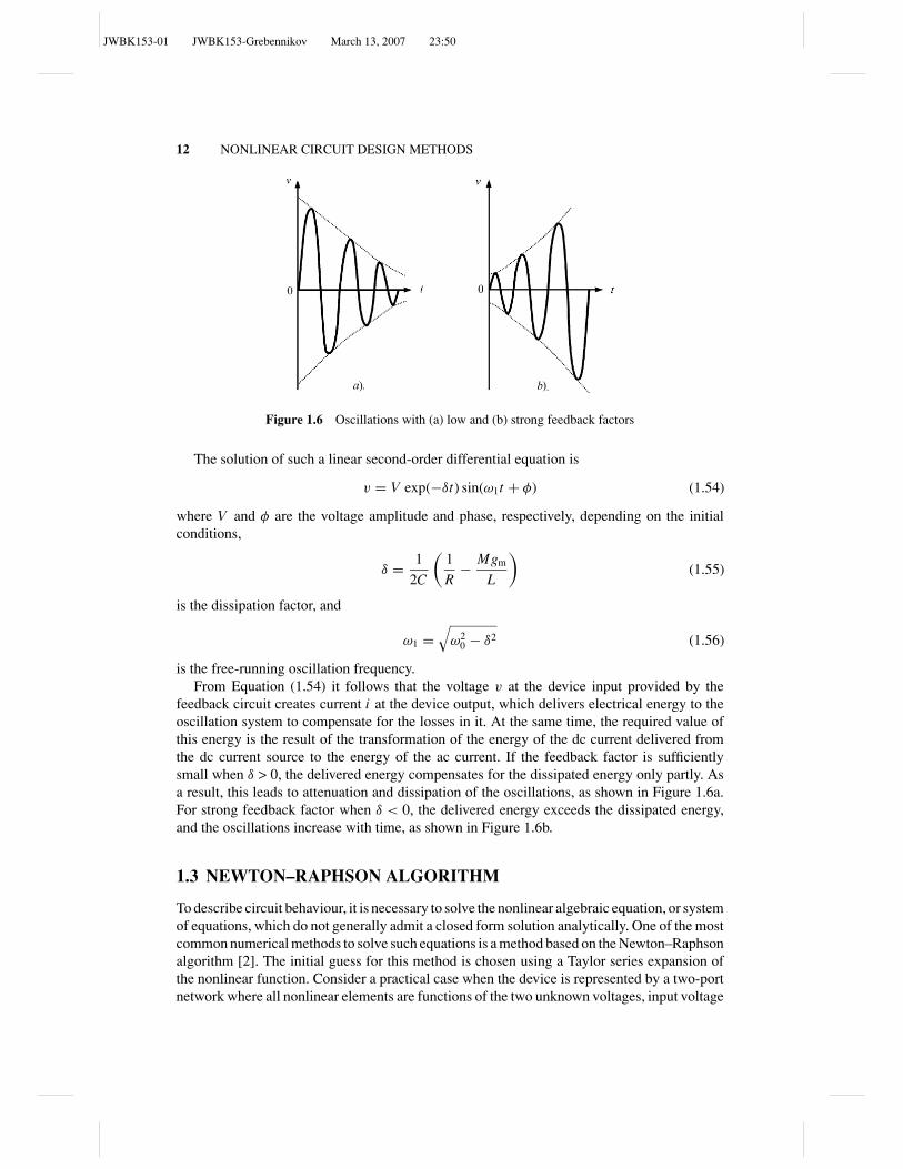
Figure 1.6 Oscillations with (a) low and (b) strong feedback factors
The solution of such a linear second-order differential equation is
v = V exp(−δt) sin(ω1t + φ) (1.54)
where V and φ are the voltage amplitude and phase, respectively, depending on the initialconditions,
δ = 1
2C
(1
R− Mgm
L
)(1.55)
is the dissipation factor, and
ω1 =√
ω20 − δ2 (1.56)
is the free-running oscillation frequency.From Equation (1.54) it follows that the voltage v at the device input provided by the
feedback circuit creates current i at the device output, which delivers electrical energy to theoscillation system to compensate for the losses in it. At the same time, the required value ofthis energy is the result of the transformation of the energy of the dc current delivered fromthe dc current source to the energy of the ac current. If the feedback factor is sufficientlysmall when δ > 0, the delivered energy compensates for the dissipated energy only partly. Asa result, this leads to attenuation and dissipation of the oscillations, as shown in Figure 1.6a.For strong feedback factor when δ < 0, the delivered energy exceeds the dissipated energy,and the oscillations increase with time, as shown in Figure 1.6b.
1.3 NEWTON–RAPHSON ALGORITHM
To describe circuit behaviour, it is necessary to solve the nonlinear algebraic equation, or systemof equations, which do not generally admit a closed form solution analytically. One of the mostcommon numerical methods to solve such equations is a method based on the Newton–Raphsonalgorithm [2]. The initial guess for this method is chosen using a Taylor series expansion ofthe nonlinear function. Consider a practical case when the device is represented by a two-portnetwork where all nonlinear elements are functions of the two unknown voltages, input voltage

JWBK153-01 JWBK153-Grebennikov March 13, 2007 23:50
NEWTON–RAPHSON ALGORITHM 13
vin and output voltage vout. As a result, after combining linear and nonlinear circuit elements,a system of two equations can be written as
f1(vin, vout) = 0 (1.57)
f2(vin, vout) = 0 (1.58)
Assume that the variables vin0 and vout0 are the initial approximate solution of a systemof Equations (1.57) and (1.58). Then, the variables can be written as vin = vin0 + �vin andvout = vout0 + �vout, where �vin and �vout are the linear increments of the variables. Applyinga Taylor series expansion to Equations (1.57) and (1.58) yields
f1(vin0 + �vin, vout0 + �vout) = f1(vin0, vout0) + ∂ f1
∂vin
∣∣∣∣vin=vin0
vout=vout0
�vin
+ ∂ f1
∂vout
∣∣∣∣vin=vin0
vout=vout0
�vout + o(�v2
in + �v2out + . . .
) = 0 (1.59)
f2 (vin0 + �vin, vout0 + �vout) = f2 (vin0, vout0) + ∂ f2
∂vin
∣∣∣∣vin=vin0
vout=vout0
�vin
+ ∂ f2
∂vout
∣∣∣∣vin=vin0
vout=vout0
�vout + o(�v2
in + �v2out + . . .
) = 0 (1.60)
where o(�v2in + �v2
out + . . .) denotes the second- and higher-order components.By neglecting the second- and higher-order components, Equations (1.59) and (1.60) can
be rewritten in matrix form
−[
f1
f2
]=
⎡⎢⎢⎣∂ f1
∂vin
∂ f1
∂vout
∂ f2
∂vin
∂ f2
∂vout
⎤⎥⎥⎦ [�vin
�vout
](1.61)
In the phasor form,
−F = J�v (1.62)
where J is the Jacobian matrix of a system of Equations (1.57) and (1.58).The solution of Equation (1.62) for a nonsingular matrix J can be obtained by
�v = −J−1 F (1.63)
This means that if
v0 =[
vin0
vout0
](1.64)
is the initial guess of this system of equation, then the next (more precise) solution can bewritten as
v1 = v0 − J−1 F (1.65)
where
v1 =[
vin1
vout1
](1.66)

JWBK153-01 JWBK153-Grebennikov March 13, 2007 23:50
14 NONLINEAR CIRCUIT DESIGN METHODS
Figure 1.7 Circuit schematic with resistor, diode, and voltage source
Thus, starting with initial guess v0, we compute v1 at the first iteration. For the iterationn + 1, we can write
vn+1 = vn − J−1 F(vn) (1.67)
The iterative Equation (1.67) is given for a system of two equations; however it can bedirectly extended to a system of k nonlinear equations with k unknown parameters. Thisiterative procedure is terminated after (n + 1) iterations whenever
|xn+1 − xn| =√√√√ K∑
k=1
(xk
n+1 − xkn
)2< ε (1.68)
where ε is a small positive number depending on the desired accuracy. For a practical purpose,it is desirable that the Newton–Raphson algorithm should converge in a few steps. Therefore,the choice of an appropriate initial guess is crucial to the success of the algorithm.
Consider the circuit shown in Figure 1.7. According to Kirchhoff’s voltage law,
v = vR + vD (1.69)
where vR = i R.
The electrical behaviour of the diode is described by
i(vD) = Isat
[exp
(vD
VT
)− 1
](1.70)
Rearranging Equation (1.70) gives the equation for vD in the form
vD = VT ln
(i
Isat+ 1
)(1.71)
Thus, from Equations (1.60) and (1.61) it follows that
v = i R + VT ln
(i
Isat+ 1
)(1.72)
This allows current i to be determined for a specified voltage v. However, because it isimpossible to solve this equation analytically for current i in explicit form, the solution mustbe found numerically.
Consider a dc voltage source V with dc current I . For the sinusoidal voltage source, it isnecessary to calculate the Bessel functions for dc, fundamental-frequency and higher-order