review deep impurity-center ionization by far-infrared ... · review deep impurity-center...
TRANSCRIPT

REVIEW
rst
Deep impurity-center ionization by far-infrared radiationS. D. Ganichev* and W. Prettl
Institut fur Angewandte Physik, Universita¨t Regensburg, D-93040 Regensburg, Germany,
I. N. Yassievich
A. F. Ioffe Physicotechnical Institute, Russian Academy of Sciences, 194021 St. Petersburg, Russia~Submitted April 21, 1997!Fiz. Tverd. Tela~St. Petersburg! 39, 1905–1932~November 1997!
An analysis is made of the ionization of deep impurity centers by high-intensity far-infrared andsubmillimeter-wavelength radiation, with photon energies tens of times lower than theimpurity ionization energy. Within a broad range of intensities and wavelengths, terahertz electricfields of the exciting radiation act as a dc field. Under these conditions, deep-centerionization can be described as multiphonon-assisted tunneling, in which carrier emission isaccompanied by defect tunneling in configuration space and electron tunneling in the electric field.The field dependence of the ionization probability permits one to determine the defecttunneling times and the character of the defect adiabatic potentials. The ionization probabilitydeviates from the field dependencee(E)}exp(E2/Ec
2) ~whereE is the wave field, andEc
is a characteristic field! corresponding to multiphonon-assisted tunneling ionization in relativelylow fields, where the defects are ionized through the Poole–Frenkel effect, and in verystrong fields, where the ionization is produced by direct tunneling without thermal activation.The effects resulting from the high radiation frequency are considered and it is shownthat, at low temperatures, they become dominant. ©1997 American Institute of Physics.@S1063-7834~97!00111-1#
INTRODUCTION semiconductors at high excitation levels, which was fi11
an
o1e
ent
su
cthumoranwh
anT
igtaroy
estors
,kirgestricisn-to
heerlykeveopye inighs.idthn ofofos-dythe
7/
The interest in the spectroscopy of semiconductorssemiconductor structures in the far-infrared~FIR! and sub-millimeter ~SBM! ranges~wavelengths extending from 30 t1000 mm, corresponding to photon energies from 35 tomeV! is stimulated primarily by the fact that they include thcharacteristic energies of many elementary excitationssemiconductors. Among these are the plasma oscillationergy, the ionization energies of typical shallow donors aacceptors, the cyclotron and spin interaction energies,characteristic size-quantization energies of the electronsystem, optical phonon energies etc. For many decadesFIR and SBM ranges have been among the hardest to acexperimentally. The advent of novel radiation sources inrecent twenty to thirty years has made possible a large nber of experiments making use of grating monochromatFabry–Perot interferometers, backward-wave tubes,relatively lower-power, electrically or optically pumped clasers emitting discrete lines. SBM and FIR spectroscopybecome an efficient tool in studies of material propertiesof the various phenomena in different areas of research.appearance of high-power pulsed FIR and SBM lasers~firstof the TEA CO2-pumped, molecular-gas type1,2 and, subse-quently, of free-electron lasers3,4 and p-Ge semiconductordevices5–10! capable of delivering nanosecond pulses of hintensity, up to a few MW, has opened up totally new visin investigation of semiconductors in the FIR range and pvided a basis for development of far-infrared spectroscop
1703 Phys. Solid State 39 (11), November 1997 1063-7834/9
d
inn-dheb-theesse-
s,d
asdhe
hs-
of
made use of at the Ioffe Physicotechnical Institute.In this frequency range, the high radiation intensity giv
rise to a variety of nonlinear phenomena in semiconducand semiconductor structures~see, e.g., review12!, such as,for example, multiphoton absorption,13–19 absorption satura-tion ~bleaching!,20–30 nonlinear cyclotron resonance,31,32 im-pact ionization,33,34 nonlinear photoacoustic spectroscopy35
high-harmonic generation,36,37 and the high-frequency Stareffect,38 whose characteristics differ substantially from thecounterparts observed both in the visible and infrared ranand in the range extending from microwaves to dc elecfields. The reason for this lies in that the FIR–SBM rangeactually a domain where the interaction in the electrophoton system undergoes a transition from the quantumclassical limit, thus creating a unique possibility to study tsame physical phenomenon in conditions where by propvarying the frequency or intensity of radiation one can madominant either the discrete properties of light or its wacharacteristics. Submillimeter and far-infrared spectroscat high-excitation levels has also an essential advantagthat it makes a technique more sensitive due to the hintensity of radiation, i.e. to the larger number of photonSince the photon energy is here much less than the gap wand, hence, there can be no direct one-photon generatiofree carriers, observation of the relatively weak effectscarrier redistribution in momentum and energy becomes psible. The high radiation intensity permits one also to stuin detail such photoelectric phenomena as, for instance,
1703111703-24$10.00 © 1997 American Institute of Physics

linear and nonlinear electron-gas heating,21,29,33,34,39–44pho-45,46
rg-
pweerlo-a
g
engiotioAesreth
ecer
iumoacuecore
t o
erkeabyittredmdsn
heththtndno
n-
der contactless application of a strong uniform electric fieldanp-in
heuc-of
epa-a-is-ts ofichos-il theica-yhemainndnd
role
theon-inceintion
ingdi-, ased
osi-n-thera-
on1.to
le-ns
za-re
ns.as
o-ithhenic
toelectric phenomena associated with Bloch oscillations,photon drag of electrons,11,15,47–52photogalvanic effect,53–57
photoresistive effects produced in semiconductor structuin plasma reflection,58–62and multiphoton resonant tunnelinin quantum-well structures,18 as well as to use them in development of radiation detectors.47,50,51,63–68
This work deals with the new nonlinear effect of deeimpurity ionization by FIR radiation at photon energies a fetens of times lower than the impurity binding energy rported in Ref. 69. We are going to consider impurity centwith no direct coupling of light to localized vibrationamodes. The ionization process is studied by the photocductivity method,70 which is traditionally used in optical research and is capable of detecting extremely sm(,0.01%) changes in carrier concentration, thus providinhigh measurement sensitivity.
If there are no free carriers in the semiconductor, deimpurities can be ionized through tunneling in the stroelectric field of the radiation. In most cases, the FIR radiatacts here as a strong dc electric field, and the ionizaprobability does not depend on the radiation frequency.increase of the frequency and decrease of temperature rin the ionization probability becoming dependent on fquency, which signals the transition to the case whenmagnitude of the photon energy becomes significant.
Deep impurity centers play a dominant part in the eltronic properties of semiconductor materials and have thfore become a subject of extensive investigation.71–77 It isthe deep centers that determine usually the nonequilibrcarrier lifetimes by acting as centers of nonradiative recobination and thermal ionization. Investigation of the effectelectric field on thermal ionization and carrier trapping hbeen traditionally used to probe deep impurities. In partilar, investigation of the ionization or capture in a strong eltric field is actually the only way to find the parametersthe multiphonon transitions determining the nonradiativecombination rate. Deep-level transient spectroscopy~DLTS!is also among the most extensively employed tools. Mosthe deep-center parameters~ionization energy, nonradiativeand radiative trapping cross sections! were obtained usingvarious modifications of DLTS. It should be noted, howevthat nonuniformities of the electric field in a structure mainterpretation of the results obtained difficult. Direct appliction of strong static electric fields is usually complicatedthe onset of field nonuniformities in the sample and qufrequently initiates avalanche breakdown. Using the elecfield of high-intensity, short laser pulses in the far-infrarrange at THz frequencies avoids such problems and percontactless and uniform application of strong electric fielDespite the high radiation intensities involved, there is noor only insignificant heating of the electron gas or of tcrystal lattice under these conditions. This is the result ofextremely weak absorption of the FIR radiation due tolow concentration of free carriers~the carriers are frozen ouon the centers!, as well as to the use of short, nanosecorange pulses, which do not perturb substantially the phosystem.
Thus discovery of multiphonon tunneling ionization u
1704 Phys. Solid State 39 (11), November 1997
es
-
-s
n-
lla
p
nnnult
-e
-e-
m-
fs--f-
f
,
-
eic
its.e
ee
-n
and using short radiation pulses with duration shorter ththe nonequilibrium carrier lifetimes has permitted develoment of a new method for probing deep impurity centerssemiconductors, offering a possibility of determining tmultiphonon parameters of deep-level impurities, the strture of their adiabatic potentials, and the trapping kineticsnonequilibrium carriers.
The present review deals with the ionization of deimpurity centers by high-intensity, pulsed FIR–SBM radition. Section 1 considers the theory of deep-impurity ioniztion by a dc and high-frequency electric field, Sec. 2 dcusses the experimental techniques used and subjecinvestigation, Sec. 3 analyzes the conditions under whone observes tunneling ionization and considers other psible mechanisms, Sec. 4 presents and discusses in detarelevant experimental results, Sec. 5 looks into the appltion of the method of multiphonon impurity ionization bFIR–SBM radiation to studies of relaxation dynamics in tparticular case of the trapping kinetics of nonequilibriucarriers in GaP:Te, and Sec. 6 sums up the review with mconclusions. The Appendix includes effects of linear anonlinear electron-gas heating by far-infrared radiation, ait shows that these phenomena do not play a significantin the experiments discussed here.
1. DEEP-IMPURITY IONIZATION BY AN ELECTRIC FIELD
1.1. Adiabatic approximation
The binding energy of deep centers exceeds by faraverage phonon energy, and therefore only multiphonassisted processes can give rise to thermal emission. Selectronic transitions occur much faster than transitionsthe phonon system, one can use the adiabatic approximain the description of electron-phonon interaction.78
Consider the simplest case of the deep impurity havonly one bound state. Obviously enough, this model isrectly applicable to the capture by neutral centers, andthis will be shown in Sec. 1.5, the main conclusions reachhere remain valid also for deep attractive centers. The ption of the localized level is determined by the potential geerated by the impurity and is substantially dependent ondistance from the impurity to the nearest atoms. Thus vibtions of the impurity and of the lattice modulate the positiof the localized electronic level, as this is shown in Fig.Strong thermal vibrations can eventually drive the levelcontinuum, thus producing ionization of the impurity.79
Quantitative consideration is usually made using a singmode model, which describes the impurity vibratiothrough variation of only one configuration coordinatex.This approximation is valid, because the multiphonon ionition of deep impurities and the trapping by the latter adominated by the breathing mode of localized vibratioThe adiabatic approximation treats electronic transitionsoccurring at a fixed configuration coordinatex, with the vi-brations of the impurity itself being determined by the ptential, which is generated by the surrounding atoms, wdue inclusion of the mean polarization field induced by tlocalized electron. Such potential averaged over electro
1704Ganichev et al.

rg
n---po-on
bound to the impurity, andU2(x), to that of an ionized im-n-
lec-e
dnones
. 2,al
the
di-
on-
us
ityfecve
motion is called adiabatic, and it includes the electron eneat a fixed coordinatex.
Figure 2 shows two main possible configuratiocoordinate diagrams:~a! for the case of weak electronphonon coupling and~b! for strong electron-phonon interaction, where self-trapping occurs, as is the case, for examwith DX and EL2 centers in III-V semiconductors. The ptential curveU1(x) corresponds to the case of the electr
FIG. 1. Modulation of a localized electronic level by the vibrating impurand lattice. a! ground-state bound electron, vibrational system of the dein equilibrium; b! defect vibrational system perturbed, the electronic leapproaches the continuum.
y
le,
purity and a free electron with zero kinetic energy. The eergy separating the two potentials is determined by the etron binding energy«b(x) at a fixed configuration coordinatx:
U1~x!5U2~x!2«b~x!. ~1!
The equilibrium positions of the ground state~with the elec-tron bound to the impurity! and the ionized state are shiftewith respect to one another as the result of electron-phocoupling. Accordingly, the optical-ionization energy, by thFranck–Condon principle, can be written a«opt5«b(x5x0), wherex0 is the equilibrium value of theground-state configuration coordinate. As seen from Figthe energy of optical ionization is larger than that of thermionization «T . The relaxation energyD«5«opt2«T charac-terizes the electron-phonon coupling strength, sincestronger is the coupling, the larger isD«. The electron-phonon coupling can be conveniently characterized by amensionless parameter
b5D«
«T. ~2!
The configuration of Fig. 2a corresponds to weak electrphonon coupling (b,1), and the difference between«opt
and«T is, as a rule, small. Actually, no difference has thbeen observed between«opt and «T in germanium and sili-
tl
, as is the
FIG. 2. Two main possible configurational diagrams. a. weak electron-phonon coupling, b. strong electron-phonon coupling allowing self-trappingcase, for instance, with DX centers in III-V semiconductors. Shown below are the tunneling trajectories on an enlarged scale.1705 1705Phys. Solid State 39 (11), November 1997 Ganichev et al.

con. There are, however, cases, where the relaxation energy,
s--t
th
risesityno
lech
s
mitcoptp
on
c-
thmat
-
at-heth
ro
ability increases. On the other hand, the population of the
ti-
mi-s aer,er-
ed
he
at
n-ra-
ry,
2,
o-n-
2a
linglf-
eicn-
is fairly high, for instance, with the oxygen impurity in GaPwhich is in state 2, whereb50.56.75,80
The configuration-coordinate diagram of Fig. 2b illutrates the case ofb.1, where the optical and thermal ionization energies differ considerably. This diagram is useddescribe, for instance, the DX and EL2 centers, wheredifference was experimentally revealed.71,74–77 Such self-trapped states have a large potential barrier suppressingreturn of free electrons to the localized state, thus givingto the phenomenon of persistent photoconductivity. In thconditions, there is no radiative capture into the impurstate. The various features of the adiabatic configuratiopotentials play an essential role in nonradiative trappingfree carriers.75 We shall restrict ourselves to the simpmodel of two identical displaced parabolic curves, whiwas first proposed by Huang and Rhys78 and is presentlywidely employed in the theory of multiphonon transitionBy this model
U1~x!5Mv2x2
2~3!
U1~x!5Mv2~x2x0!2
22«T, ~4!
whereM is the mass of the impurity, andv is the vibrationalfrequency.
1.2. Multiphonon-assisted thermal emission
Consider first thermally-activated carrier emission froa deep center with no electric field present. For simplicand definiteness, we shall consider electrons, although asiderable part of measurements were carried out on accein Ge and Si. The model to be treated here is equally apcable to the electrons and holes.
Classical approximation gives the following expressifor the emission probability
e}exp2S «T1«2
kBT D , ~5!
where«25U1(xc), andxc is the coordinate at the intersetion of the potentialsU1(x) andU2(x), at which the electronbinding energy is zero,«b(xc)50 ~see Fig. 2!. Thus«T1«2
is actually the lowest excitation energy required to detachelectron within the classical approach to the motion of ipurities. The model of Huang and Rhys, where the adiabpotentials U1(x) and U2(x) are two identical paraboliccurves, «25(«T2D«)2/4D«. In the weak-binding case(D«!«T), where«2@«T , no process with an activation energy «T1«2 was ever observed to follow relation~5!. Usu-ally the activation energy is much less than«T1«2 , sincethe electron is emitted from the vibrational level lying«T1E ~the energyE is reckoned from the minimum of potential U2 , andE,«2! because the defect tunnels from tconfiguration corresponding to the ground state to that ofionized impurity ~Fig. 2!. As the vibrational energy«T1E
increases, the tunneling barrier separating theU1 and U2
potentials becomes lower, and, hence, the tunneling p
1706 Phys. Solid State 39 (11), November 1997
ois
theee
alf
.
yn-
orsli-
e-ic
e
b-
«T1E level decreases with increasingE proportional toexp(2E /kBT). Thus for each temperature there is an opmum energyE5E0 , at which the tunneling probability isthe largest.75,81–83
We shall consider the defect tunneling process in seclassical approximation. In this approach, the particle hawell defined trajectory even under the potential barriwhere the kinetic energy is negative. The probability of thmally activated emission of a defect,P(E), with a vibra-tional energy«T1E at a temperatureT is given by the ex-pression
P~E !}exp~2c! ~6!
with
c~E !5«T1E
kBT12uS~E !u, ~7!
whereS(E) is the action multiplied byi /\. The first term inEq. ~7! describes the population of the«T1E level, and thesecond, the defect tunneling from the ground to an ionizstate. SinceP(E) depends exponentially on energyE , tun-neling occurs within a narrow energy interval close to tenergy of optimum tunnelingE0 ~see Fig. 2!. This optimumtunneling energy is determined by the vibrational energywhich C(E) has a minimum:
dc
dEU
E5E0
52duS~E !u
dEU
E5E0
11
kBT50. ~8!
The derivativeduSu/dE in Eq. ~8! multiplied by\ deter-mines the tunneling time through the barriert.84,85 Thus inthe case of multiphonon tunneling ionization the time of tuneling by the optimum trajectory is determined by tempeture and is\/kBT.
Following Refs. 75, 81–83,S(E) can be divided intotwo parts:
S~E !52S1~E !1S2~E !, ~9!
Si~E !5A2M
\ Eai
xcdxAUi~x!2E , i 51,2, ~10!
corresponding to two parts of the tunneling trajectonamely, 1, under potentialU1 , from the turning pointa1 topoint xc , where the adiabatic potential curves cross, andunder potentialU2 , from a2 to xc . The actual direction oftunneling along thex coordinate is specified by the sign ofSi
in Eq. ~9!. The tunneling trajectories for both adiabatic ptential configurations are denoted in Fig. 2 by arrows. Tuneling in the two configurational potentials shown in Figs.and 2b is essentially different in thatS1(E) andS2(E) havethe same sign in the case of weak electron-phonon coupwith b,1 ~Fig. 2a! and opposite signs in the case of setrapping, b.1 ~Fig. 2b!.86 Recalling that uS2u.uS1u wecome touS1u5uS2u2uS1u for the configuration of Fig. 2a, andto uSu5uS1u1uS2u for the self-trapping case. Introduce thtunneling timest1 andt2 under the corresponding adiabatpotentials for the optimum energy of thermally activated tuneling:
1706Ganichev et al.

duSi u M xc dx
o
-
la-
ong
th
idnay-thtte
nttiaw
rie
rg
ndeldn
rstia
ic
t.ith
mial
h
ityp-
ngy.
t i5\dE
UE5E0
5A2 U E
ai AUi~x!2E0U i 51,2.
~11!
Equations~8! and ~11! yield
t5t26t15\
2kBT~12!
where the minus sign corresponds to the configurationFig. 2a, and the plus, to that of Fig. 2b. SinceE0 is usuallymuch less than«T , the timet1 is practically temperatureindependent and can be calculated forE050.
In the case of weak electron-phonon coupling («2@«T),Eq. ~8! yields within the Huang–Rhys model a simple retion for the optimum defect-tunneling energyE0
E05«T /@exp~\v/kBT!21#. ~13!
which shows that in the low-temperature domain (kBT,\v)we indeed haveE0!«T . SettingE050 in Eq. ~11! in thecalculation oft1 we come to
t15AM
2 Ea1
xc dx
AU1~x!~14!
Equation ~14! yields in the case of weak electron-phoncoupling, b,1, the following expression for the tunnelintime t1 :
t151
2vln
«T
«opt2«T~15!
and for the self-trapping case (b.1):
t151
2vln
«opt2«T
«T. ~16!
Thus Eq.~12! defines the temperature dependence oftunneling timet2 .
1.3. Multiphonon-assisted tunneling ionization in an electricfield
Carrier emission in static electric fields was first consered in Ref. 87 and calculated numerically in Ref. 88; alytical expressions for the probability of deep impuritcenter ionization were obtained in Refs. 89, 90, andsubsequent analysis will draw essentially from the laworks.
In a uniform electric field, the potential with a constaslope in the field-vector direction is added to the potenwell binding the electron to the impurity. The electron is nocapable of tunneling through the triangular potential barthus formed at a negative kinetic energy2« ~Fig. 3!, withthe corresponding adiabatic potential shifted down in eneU2«5U22« ~dashed line in Fig. 2!. In these conditions, thedefect tunneling trajectory in configuration space shorteand the barrier height becomes lower. We start by consiing the case of high temperatures and relatively weak fiewhere the field introduces a correction only to thermal ioization, and« is much smaller thanE0 . The optimum defecttunneling energyE0 remains here unchanged, and, to fiorder in«, the correction to the argument of the exponen
1707 Phys. Solid State 39 (11), November 1997
f
e
--
er
l
r
y,
s,r-s,-
tl
C determining the ionization probability@see Eqs.~6! and~7!# can be found by varying in« the functionS(E0 ,«) de-fined by Eqs.~9! and ~10!, with U2 being replaced byU2« .We obtain
c~E0 ,«!5cu«5012duS2«u
d« U«50, x«5const
, ~17!
where
S2«5A2M
\ Ea2
xcdxAU2~x!2«2E0. ~18!
The probability for a thermally-emitted carrier with kinetenergy2« now becomes
e~«!5e~0!exp~2«t2 /\! ~19!
wheret2 is the tunneling time defined by Eq.~11!, ande(0)is the ionization probability with no electric field presenThe increase of the probability of electron emission wenergy2« by the factor exp(2«t2 /\) is primarily due to thelowering of barrier height when the defect is tunneling fropoint xc to the turning point under the adiabatic potentcurve U2« at the vibrational levelE0 . While this factorgrows with «, the probability of electron tunneling througthe triangular barrier whose height is determined by« ~seeFig. 3! drops rapidly proportional toexp@2(4«2/3A2m* /(3\eE)#, where E is the electric field,and m* is the electron effective mass. Thus the probabilof multiphonon tunneling ionization with the electron escaing with a negative energy2« can be written as
FIG. 3. Potential barrier for the electron in a dc electric field directed alothez axis.«b is the electron binding energy,« is the electron escape energ
1707Ganichev et al.

e~E,«!}exp~2«t /\!exp 24 «3/2A2m*
. ~20!
y
er
ngt
iothricthc-
of
to
-
der
er
isthb-
inheoecl-
th
ofatic
revi-
aw-i-
gh
ac-n
nifi-
e-the
te.to
n
2 S 3 \eE DThe exponential behavior ofe(E,«) results in the existenceof an optimum electron energy2«m determined by themaximum of the exponential in Eq.~20!:
«m5t2
2e2E2
2m*~21!
This optimum electron energy«m corresponds to the energat which the time of electron tunneling in an electric fieldEis equal to the timet2 determining the defect tunneling undthe potential curveU2 at the vibrational levelE0 optimumfor thermally stimulated tunneling. Indeed, the tunnelitime in an electric fieldE under a triangular barrier of heigh« is given by the relation
te5Am*
2 E0
zf dz
A~«2eEz!5
A2m* «
eE. ~22!
As follows from Eqs.~21! and~22!, te5t2 for «5«m . Thusthe result obtained has a simple physical interpretatnamely, the optimum electron energy is determined byequality of the tunneling time of the electron in an electfield to that of the defect in configuration space underpotential U2 corresponding to the defect without the eletron.
Inserting«m thus found into Eq.~20! yields for the mul-tiphonon tunneling ionization probability as a functionelectric field the following expression:
e~E!5e~0!expS E2
Ec2D 5e~0!expS t2
3e2E2
3m* \ D . ~23!
The emission in an electric field increases by a facexp(E2/Ec
2), whereEc25(3m* \)/(t2
3e2) is the characteristicfield determined by the tunneling timet2 and, hence, depending on temperature. As seen from Eqs.~23! and~12!, theionization probability grows exponentially with squareelectric field, and increases rapidly with decreasing tempture. The increase of the ratioe(E)/e(0) with decreasingtemperature is accounted for by the fact that at low temptures the optimum energyE0 for thermally stimulated tun-neling tends to zero, and the tunneling timet2 grows toinfinity. Hence a small decrease of the adiabatic potentialU2
of an ionized impurity leads to a large increase of the emsion probability. The temperature and field behavior ofcarrier emission probability in a dc electric field was oserved to follow Eq.~23!.90–92
1.4. Direct ionization by electron tunneling
The emission probability as a function of electric fieldEq. ~23! was obtained with due account of the fact that tcorrections to multiphonon emission resulting from electrtunneling are small, in other words, that the energy of eltron tunneling«m is much smaller than that of defect tunneing E0 and of thermally stimulated ionization«T . This con-dition defines the upper bound on the electric field whereconsideration presented in Sec. 1.3 is valid:
1708 Phys. Solid State 39 (11), November 1997
n,e
e
r
a-
a-
-e
n-
e
E!E0/2vt2 ~24!
where
E052vA2m* «T
e. ~25!
In the opposite limit,E@E0 , direct carrier tunneling fromthe ground state to continuum, without participationphonons, becomes dominant. The positions of the adiabpotential curvesU2« for various electron kinetic energies ashown in Fig. 4. Direct electron tunneling occurs at thebrational level at the crossing of theU2« and U1 potentialcurves, where an electronic transition does not involvechange in the configuration coordinate. In the lotemperature limit, where thermal excitation is not likely, drect tunneling occurs at the point where theU2« curve inter-sects the minimum of potentialU1 at «5«opt. The ionizationprobability is determined here by electron tunneling throuthe triangular potential of height«opt ~Ref. 93!:
e~E!5eE
2A2m«opt
exp~2f!, ~26!
where
w54
3
«opt3/2A2m*
\eE. ~27!
As the temperature increases, one will have to take intocount the possibility of thermal activation of the impurity. Ithe case whereU2« crosses theU1 parabolic curve close toits minimum, multiphonon transitions result in a correctioto w which, while being temperature-dependent, is insigncant in the strong-field domain.90 Equations~26! and ~27!show that the emission probability in direct tunneling dpends on electric field weaker than under conditions ofmultiphonon-assisted process~Eq. ~23!.
FIG. 4. Adiabatic potentials as a function of the configuration coordinaThe potential curveU1(x) relates to the case where the electron is boundthe impurity, andU2(x), to that of the ionized impurity and a free electrowith zero kinetic energy. Dashed lines specify theU2«(x) potentials forthree characteristic cases:1 multiphonon tunneling,2 intermediate case,3direct electron tunneling.
1708Ganichev et al.

In conclusion to this Section we present a general ex-90 s
xpand
kree
oueltiys
tri
erisin-gear
el
o
d
tron-uc-
keemi-
e
s,hethe
e
–
pression obtained in the frame of the Huang and Rhymodel:
e~E !}exp~2w!, ~28!
w5«T
\vu12yuF62vt2~y!2~11j2!1/21jcosh
1
2Q G
12
3E0y3/2/E, ~29!
where
2vt2~y!51
2Q6 ln
11~11j2!1/2
j2 , Q5\v
kBT, ~30!
j5F cU12yUsinh1
2Q G21
, c5«T
D«5211
4
b. ~31!
The plus and minus signs in the expression forw refer to thecases ofy,1 andy.1, respectively, and the value ofy isfound by solving the equation
~E/E0!Ay52vt2~y!. ~32!
The above expressions determine the character of the enential dependence within a broad range of electric fieldstemperatures and reduces to the limiting cases describeEqs.~23! and ~26!.
1.5. Charge effect
Most deep centers bear a charge, which should be tainto account when considering ionization processes. Thethe well-known Poole–Frenkel effect consisting in a dcrease of the thermal ionization energy of attractive Clomb centers in the presence of an external electric fiwhich lowers the barrier generated by the Coulomb poten~see Fig. 5!. The theory of this effect was developed bFrenkel,94 who showed that the ionization probability growexponentially with the square root of the external elecfield. The Poole–Frenkel effect is a dominant mechanismthe increase of the ionization probability of attractive centby electric field for not too high fields, where the ejectiondominated by over-barrier emission, and carrier tunneldoes not play a significant role.75 This phenomenon was observed in I 2V characteristics under a dc bias in a larnumber of insulators and semiconductors. Straightforwcalculation shows that application of an electric fieldE low-ers the ionization barrier in the direction opposite to the fi~Fig. 5b! by an amount«PF :
«PF52AZe3E
¸, ~33!
whereZ is the charge on the center, and¸ is the dielectricconstant.
As a result, an electric field increases the probabilitythermal emission
e~E!}exp~«PF /kBT!. ~34!
The general theory of the Poole–Frenkel effect and theviations from the simple relations~33! and ~34! are consid-
1709 Phys. Solid State 39 (11), November 1997
o-dby
enis--
d,al
cins
g
d
d
f
e-
ered in detail in Ref. 83. It can be shown75,95that inclusion ofmultiphonon effects results inkBT in Eq. ~34! being replacedby kBT* , where
1
kBT*5
t2
\5
1
kBT6
2t1
\. ~35!
The plus sign corresponds here to the case of weak elecphonon coupling, and the minus, to self-trapping, thus reding or increasing, respectively, the slope of the ln@e(E)#}AE relation.
Obviously enough, the Poole–Frenkel effect can taplace in relatively weak fields, where the lowering of thbarrier does not exceed the Coulomb energy scale in seconductors, i.e. in electric fieldsE lower than the field deter-mined from the equation «PF(E)5Z2Ry* , whereRy* 5e4m* /2¸2\2 is the effective electron energy in thCoulomb potential of a charged impurity~the Rydberg en-ergy!. In stronger electric fields or at lower temperaturetunneling effects become dominant, with the role of tcharge being reduced to increasing the transparency ofbarrier through the lowering of its height. In this limit on
FIG. 5. Coulomb potential of an attractive impurity~a! with no electric fieldand ~b! in the presence of a dc electric field applied along thez axis.«b—binding energy,«PF—lowering of the potential barrier by the PooleFrenkel effect.
1709Ganichev et al.

can readily obtain an expression for the correction to then
-e
rgd
nions
sr
tenndgo
oni
ithin
epfo
en
gh
eiod
tn
an
threre
c-
rrsttun-ialbedrgy,n.
as-ac-
ti-
n-helyn
he
fect
en-
tial
r,
probability of tunneling ionization involving a multiphonotransition. In the limit that«m.Ry* , this correction calcu-lated in Ref. 95 produces an additional factor in Eq.~23! forthe emission probabilitye(E). Taking into account the Coulomb charge, the probability of multiphonon-assisted tunning ionization can be written as
e~E!5e~0!expF2A2m* Ry!
eEt2lnS 4t2
3e2E2
m* \ D GexpS t23e2E2
3m* \ D .
~36!
We readily see that the correction due to the impurity chain Eq. ~36! tends to unity with increasing electric field anbecomes insignificant in strong fields.
Thus taking into account the Poole–Frenkel effect amultiphonon tunneling ionization we come to the conclusthat the log ionization probability grows with the field first aAE and, in the high-field domain, asE2.
1.6. Ionization by submillimeter radiation
The choice between the quantummechanical and clacal treatment of an electromagnetic field depends on thelation between the period of the radiation fieldV21 and thecharacteristic times of the processes occurring in the sysunder study. Keldysh96 showed that multiphonon ionizatioof semiconductors under high-frequency illumination atunneling ionization in a dc electric field are just two limitincases of the same nonlinear process. It was also demstrated that, for a given incident intensity, the ionizatiprobability increases with frequency, and that this growthcharacterized by a parameterVte , wherete is the electronunder-barrier tunneling time in the electric wave field, wthe barrier height determined by the ground-state bindenergy. These results~see also Ref. 97! are fully applicableto analyzing direct electron tunneling ionization from decenters. For these conditions, the height of the barrierelectron tunneling is determined by the electron bindingergy with the impurity at equilibrium, i.e. by«opt. The timerequired for an electron to tunnel through a barrier of hei«opt in an electric fieldE can be written
t5A2m* «opt
eE. ~37!
If for the value ofE corresponding to the maximum wavfield amplitude this time is shorter than the wave perV21, i.e.
V,eE
A2m* «opt
, ~38!
then the action of the high-frequency field is equivalentapplication of a dc electric field. The tunneling ionizatioprobability does not depend in this case on frequency,the tunneling probability is given by Eqs.~26! and ~27!. Asfollows from Ref. 96, where a general expression forelectron transition probability was obtained for the total fquency range, one can readily derive the frequency cortion to the exponential factor in Eq.~26! if condition ~38! ismet:
1710 Phys. Solid State 39 (11), November 1997
l-
e
d
si-e-
m
n-
s
g
r-
t
o
d
e-c-
w54
3
A2m* «opt3/2
\eE S 12m* V2«opt
5e2E2 D . ~39!
The effect of a high-frequency electric field on the ejetion probability is due to two mechanisms, namely,~i! barriermodulation, and~ii ! a possibility of tunneling at a lowebarrier height through absorption of photons. While the fimechanism brings about an exponential decrease of theneling probability, the second results in its exponentgrowth. As the frequency is increased, the energy absorin tunneling increases too and tends to the binding enethus resulting in ionization through multiphonon absorptioThe ejection probability also grows in this case with increing frequency, since the photon energy increases, and,cordingly, the number of photon required to initiate an opcal transition decreases~see Fig. 6!.
While in the case of multiphonon-assisted tunneling ioization the electric field does not act on the motion of tdefect itself, the tunneling of an electron should certainchange in an ac electric field. In the limit of multiphonotunneling ionization in a dc electric field~see Sec. 1.3! wefound that the optimum energy for electron tunneling«m isdetermined by the condition of the tunneling time of telectronte , ~22!, being equal to that of the defectt2 , withthe latter being determined by the temperature and devibrational frequency~12!:
te[te~«m!5t2. ~40!
The same condition determines the optimum electronergy before tunneling in an ac electric field« init52«m ~see
FIG. 6. Electron tunneling trajectory under a triangular barrier for an inienergy2«m ~1! in a dc electric field and~2! in an ac field. During thetunneling, the ac electric fieldE cos(Vt) changes the slope of the barrieand the electron absorbs photons.
1710Ganichev et al.

Fig. 6! ~note that in an ac field the initial and final tunnelingd
bere
corgtiaiate
ren-
dro
heex
eic
elysi
after the completion of the tunneling (t50) at the turning
n-
g
in-ldof
ofn
he
edion
energies are different, because energy can be absorbeding the tunneling!.
The process of multiphonon tunneling ionization candivided into three stages:~1! thermal excitation transfers thdefect with a bound electron to the vibrational level corsponding to the vibrational energy«T1E0 ; ~2! The vibra-tional system undergoes rearrangement to the potentialresponding to a free electron with a negative kinetic ene2«m , i.e. the system transfers to the adiabatic potenU2«m
; ~3! the electron tunnels to the free state with the initenergy2«m . The two latter processes are tunneling assisCondition~40! for determining the energy«m can be derivedsimilarly to the way this was done in Sec. 1.3, if one repsents the probability of electron tunneling with an initial eergy 2« in a general case by
pe~«!}exp~22Se~«!!, ~41!
where Se(«) is the electron action multiplied byi /\, andintroduces the electron tunneling timete(«) in the form
te~«!5\dSe~«!
d«. ~42!
Let us calculate now«m as a function of frequency anwave-field amplitude under the condition that the electtunneling timete is determined by the timet2 , and find theelectron tunneling probability for these conditions. In tcase of tunneling under a time-varying potential we canpressSe through the LagrangianLe ~Ref. 98!
\Se~«m!52E2te
0
Le~t!dt1«mte. ~43!
The dependence of the LagrangianLe on t is determinedby the dependence of the electron on coordinatez ~Fig. 6!and velocityz5dz/dt at timet:
Le~t!52m*
2z22Ue~z!, ~44!
whereUe is the potential energy in an electric field. All thquantities are calculated by the rules of classical mechanbut with due account of the fact that the timet is replaced byimaginary timet5 i t , since the motion takes place in thclassically forbidden region under the barrier. Accordingin the case where the electric field vector is directed oppoto thez axis we have
Ue52eEzcos~Vt !52eEzcosh~Vt!. ~45!
The tunneling trajectoryz(t) and ‘‘velocity’’ z(t)should be found from the classical equation of motion:
2m*d2z
dt2 52]U2«
]z~46!
subject to the boundary conditions
z~t!ut5te50 ~47!
for the tunneling beginning at the imaginary time2te and
z~t!ut5050 ~48!
1711 Phys. Solid State 39 (11), November 1997
ur-
e
-
r-yl
ld.
-
n
-
s,
,te
point ~see Fig. 6!.The minus sign of the second derivative in Eq.~46! ap-
pears as a result of the replacement oft by i t. Equation~46!reduces to the form
d2z
dt2 52eE
m*coshVt. ~49!
Taking into account Eqs.~47! and ~48!, Eq. ~49! yields
z5eE
m* Vsinh~Vt! ~50!
and
z5eE
m* V2 ~cosh~Vte!2cosh~Vt!!. ~51!
At the initial instant of time,t52te , the ‘‘velocity’’ isdetermined by the total electron energy2«m , because thepotential energyUe(z50)50 @see Eq.~45! and Fig. 6!#.Thus we come to the condition
z2ut52te5
2«m
m*~52!
whence follows the relation connecting«m with the tunnel-ing time te :
«m5~eE!2
2m* V2 sinh2~Vte!. ~53!
We see that for a given tunneling timete the energy«m
increases with frequency. In the limiting case of low frequecies,Vte,1, the relation between«m andte determined byEq. ~53! coincides with Eq.~22!. Note that using Eq.~43!one can readily verify that relation~42! for te does indeedhold.
Equations~41!, ~43!, ~44!, and~50! and~51! can be usedto obtain the following relation for the electron tunnelinprobability pe(E,V) for a fixed tunneling timete :
pe~E!}expH 2~eE!2
2m* V3 F2Vtesinh2~Vte!
1Vte21
2sinh~2Vte!G J . ~54!
Taking into account Eq.~53!, relation ~54! agrees with ex-ponential accuracy the result obtained in Ref. 96 and cocides with the ionization probability in an ac electric fiecalculated84 in quasi-classical approximation with the usethe vector gauge, where the scalar potential is zero.
Setting te5t2 and taking into account the increasethe defect tunneling probability under multiphonothermally-activated ionization, which is determined by tfactor exp(2«mt2 /\) @see Eqs.~19! and ~20! in Sec. 1.3#, weobtain for the resultant probability of multiphonon-assistdefect tunneling ionization under illumination an expresssimilar to Eq.~23!, where one should now substitutet2* fort2 :
e~E,V!5e~0!expS t2*3e2E2
3m* \ D , ~55!
1711Ganichev et al.

where
hn-
pt
ilit
ntoet
ch
i-br
sua
one
egin
el-af
ydoois-eore-e
ithne
fonga-
ingrva-
derlop-ce,
er-pli-e
eics
ton5–2theia-s.
serec-the
un--gered
load
theentser-hetat.tat, in
eep
TABLE I. Characteristics of the strong individual lasing lines used in thiswork.
t2*35
3
4V3 ~sinh~2Vt2!22Vt2!. ~56!
In the limit Vt2,1 we obtain from Eq.~56!:
t2*35t2
3F111
5~Vt2!2G . ~57!
We see that an increase in frequency results in a growtthe tunneling ionization probability, which is due to the icreasing initial energy of the tunneling electron«m @see Eq.~53!#, i.e. to the increase in absolute magnitude of the omum electron transition energy.
The dependence of the multiphonon emission probabon electric field amplitude@both for dc, Eq.~23!, and high-frequency, Eq.~55!, fields# was derived under the conditiothat electron tunneling gives only a small correctionmultiphonon-assisted emission, in other words, that theergy of electron tunneling«m is much less than that of defectunnelingE0 and thermal ionization energy«T . This condi-tion determines the upper limit to the electric fields for whithe above consideration is valid.
2. EXPERIMENTAL METHODS AND SUBJECTS OFINVESTIGATION
Ionization of deep impurities by high-intensity submillmeter radiation was discovered and studied in a large numof semiconductors containing such impurities. One measuthe photoresponse of a sample to pulsed radiation of amillimeter laser, which is generated by a change in free crier concentration through impurity ionization. The radiatisources used were TEA CO2-pumped, high-power tunablsubmillimeter pulsed molecular-gas lasers with NH3, CH3F,and D2O. The principle of operation of such lasers was dveloped and used to achieve cw lasing by Chang and Bridin 19691 and, in 1974, de Temple extended it to obtapulsed laser operation.2 The choice of the CO2 laser for op-tical pumping was based on the ability of tuning it within th9.2–10.6 mm-range, which includes strong vibrationarotational absorption lines of many molecules. More th1000 compounds are presently employed as gain mediaCO2-pumped lasers.99 The use for pumping of high-intensitradiation from TEA CO2 lasers operating at 100 kW anmore opens new possibilities in this respect, since the strelectric field of the light wave results in a broadeningmolecular levels and permits one to excite states fairly dtant from the pumping frequency.2 One can thus achieve lasing at a number of wavelengths which would not be accsible with low-power cw-pump radiation. The search fconditions favorable for lasing in the FIR-SBM range rduces primarily to finding appropriate gain media and linfor the CO2 pumping laser which would be in resonance wthe corresponding molecular transitions. Thousands of licovering the whole range of FIR-SBM radiation~20 mm to 2mm! have thus far been found for most of the media.99–104
Looking for new lasing lines is, however, not as essentialsemiconductor research as finding strong and stable, siradiation lines. This is particularly important for pulsed l
1712 Phys. Solid State 39 (11), November 1997
of
i-
y
n-
eredb-r-
-es
nor
ngf-
s-
s
s
rle
sers, whose high-power pump radiation results in broadenof the gain-medium molecular levels and, hence, in obsetion of a large number of additional lines.
The most sophisticated element in the laser system unconsideration is the pumping laser. In earlier days, devement of an optically pumped laser required, in the first plabuilding in the laboratory a high-power pulsed CO2 laserwith a high level of suppression of electromagnetic interfence, which was an obstacle to extending the range of apcability of high-excitation FIR-SBM spectroscopy. Now thavailability of high-stability, high-power commercial TEACO2 lasers ~URANIT 104, 204! permits one to assemblsuch a system with no difficulties at all. The characteristof strong single lines covering the range from 30 to 500mm,the corresponding gain media and lines of the TEA CO2 laserwhich are used for pumping are listed in Table I. The phoenergies corresponding to these wavelengths lie in the 3meV range and in all cases are substantially lower thanbinding energies of the deep impurities studied. The radtion pulse length varied for different lines from 10 to 100 nThe radiated power was;50 kW. The radiation was fo-cused to a spot of about 1 mm2, with the maximum intensityreaching as high as 5 MW/cm2. More details on the systemcan be found in Refs. 11, 48.
The intensity, shape and spatial distribution of the laradiations were monitored with fast noncooled photodettors operating in the submillimeter range and based onphoton drag effect,63 intrabandm-photoconductivity,64 stimu-lated tunneling effect in metal/semiconductor structuresder plasma reflection,58,66 as well as with the Spirikon pyroelectric array. The pulsed signal proportional to the chanin sample resistance under laser illumination was measuin a standard photoresponse measurement circuit with aresistanceRL550 V ~see inset to Fig. 7!. The bias voltageacross the sample, 5 V/cm, was substantially lower thanimpurity avalanche-breakdown threshold. The measuremwere carried out within the 30–150 K range, where at thmal equilibrium practically all carriers are frozen out on timpurity. The samples were placed in an optical cryosPenetration of light in the medium IR range into the cryoswas prevented by the use of crystalline quartz filters andthe visible, by a 1-mm thick black-polyethylene filter.
The tunneling ionization processes were studied on d
Wavelengthmm
Line of CO2
pump-laserMaximum intensity,
kW/cm2 Medium
35 10P ~24! 300 NH3
66 9P ~32! 100 D2O76 10P ~26! 4000 NH3
90.5 9R ~16! 5000 NH3
148 9P ~36! 4500 NH3
152 10P ~32! 3000 NH3
250 9R ~26! 400 CH3F256 10R ~14! 500 NH3
280 10R ~8! 1000 NH3
385 9R ~22! 5 D2O496 9R ~20! 10 CH3F
1712Ganichev et al.

f-
a
itim.e
ol
rIR-bytheer-
m
ve-ald itsofho-me-
.
inofof
ithob-
onrom
nb M
rily
impurity centers of two different types, namely,~i! thosewith weak electron-phonon coupling,b,1 ~Au, Hg, Cu, Znin germanium, Au in silicon, and Te in gallium phosphide!and ~ii ! with strong electron-phonon coupling where seltrapping takes place,b.1 ~tellurium in AlxGa12xSb andAl xGa12xAs!.
The thermal ionization energy of acceptor impurities«T
in germanium was 150 meV~Au!, 90 meV ~Hg!, 40 meV~Cu!, and 30 meV~Zn!, for Au in silicon—300 meV, and forthe donor tellurium in gallium phosphide, 90 meV~Ref. 75!.Note that tellurium in gallium phosphide is essentiallydeeply-buried shallow Coulomb center.
Doping with tellurium of AlxGa12xSb samples withx50.28 and 0.5, and of AlxGa12xAs with x50.35 resultedin electronic conduction, and one observed all the main fetures characteristic of DX centers, in particular, the persistephotoconductivity.105,106
3. OBSERVATION OF THE TUNNELING IONIZATION OFDEEP-IMPURITY CENTERS BY HIGH-INTENSITY FIR-SBMRADIATION
Semiconductors containing deep and shallow impurcenters have been used successfully already for a long tas low-temperature detectors in the IR and FIR ranges107
The long-wavelength limit to their use is bounded by thbinding energy of the impurity, with no response obtainefrom deep centers such as, for instance, Ge:Au and Ge:Hgthe FIR and, all the more so, in the submillimeter regionsthe spectrum. This pattern is observed, however, only at re
FIG. 7. Oscillographic traces of the excitation pulse and of the photocoductive signals generated in a sample with deep impurities illuminatedFIR–SBM radiation. Inset shows the measurement circuit.
1713 Phys. Solid State 39 (11), November 1997
a-nt
ye
dinfa-
tively low light intensities. Excitation of a semiconductocontaining generated deep impurities by strong pulsed FSBM laser radiation produced a photoconductive signalionizing the deep impurity centers, despite the fact thatpump photon energy was tens of times lower than their thmal ionization energy,«T .69,108–111A signal which increasedsuperlinearly with the incident intensity was observed froall studied samples of Ge, Si, GaP, AlxGa12xAs, andAl xGa12xSb within a broad range of temperatures and walengths employed.86 The sign of the photoconductive signcorresponds to a decrease of the sample resistance, ancharacteristic decay time is different for different typesimpurities and different temperatures. The length of the ptoresponse pulse for deep substitutional impurities is sowhat longer than that of the laser pulse~Fig. 7! and variesdepending on temperature from 100 ns to 10ms, which cor-responds to the photoexcited carrier lifetimes~see, e.g., Refs75, 112, 113!. In the case of self-trapped DX2 centers inAl xGa12xSb and AlxGa12xAs one observes an increasesample conductivity which persists for several hundredsseconds after the excitation pulse, which is characteristicthe decay of persistent photoconductivity in the samples wDX2 centers. Figure 8 compares photoresponse signalstained from an AlxGa12xSb sample on two time scales~Fig.8b! with the pump pulse~Fig 8a!. The observation of posi-tive persistent photoconductivity under FIR-SBM excitatisuggests that this signal is due to electron detachment fthe DX centers.
-y
FIG. 8. Oscillographic traces of~a! excitation pulse withl590.5mm andof the photoconductive signals generated by illuminating with FIR-SBradiation an Al0.5Ga0.5Sb sample~b! in the dark and~c! in the state ofpersistent photoconductivity produced by exposing the sample preliminato light in the near IR range.
1713Ganichev et al.

Variation of the sample conductivity induced by SBMtio
in
hern
teowthme
tinioegtroee
uma
mimole
algtohnda
ti
no
n
a
cthnge
y,inor
uqute
veia-thel-
o-
radiation can be due either to processes involving radiaabsorption by free carriers~electron gas heating,m photocon-ductivity! or to the appearance of additional free carriersionization.
We shall dwell first on the possible effect of heating tlattice or the electron gas, since this is the most natumechanism of photoconductivity under intense illuminatioCarrier heating was studied in detail in the submillimerange samples with shallow impurities and at not too ltemperatures, i.e. where the impurities are ionized andconditions are most favorable for heating. As follows frothese studies, presented in the Appendix, in the case ofcitation of samples with deep impurities, electron gas heacan be excluded as the cause of the observed impurityization based on the kinetics of the detected signals. To bwith, electron gas heating in the temperature and concention ranges considered here should produce negative phconduction, whereas the photoconductivity observed expmentally is positive. Besides, the photoresponse signal duelectron heating should either reproduce in shape the ppulse or be more complex, but it should not be longer ththe latter ~see Appendix and Refs. 39, 114!, whereas theobserved signals correspond to excited-carrier trapping tiand are substantially longer than the pump pulses. Thepurity ionization manifests itself most clearly in the casesubmillimeter-range persistent photoconductivity in sampcontaining DX centers.
Thus observation of positive photoconductive signwith times substantially in excess of the pump pulse lenexcludes electron gas heating and the corresponding phconductivity as a possible mechanism of the observed ptoresponse~see Appendix!. The suppression of heating isamples doped primarily by deep centers and maintainesufficiently low temperatures is due to carrier freezeoutimpurities and, hence, to the absence of noticeable radiaabsorption. Thus the photoresponse is indeed causedphotoionization of deep impurities by light with the photoenergy\V much less than the thermal ionization energyimpurities«T .
Figure 9 displays the dependence of the photorespoof mercury-doped germanium samples («T590 meV) onlight intensity measured atT564 K for two different wave-lengths. Shown in Fig. 10 on a semilog scale are similar dobtained for another deep impurity~gold in germanium! forthree wavelengths. The quantitiess i andsd are the sampleconductivities under illumination and in the dark, respetively. Since the pump pulse duration is shorter thannonequilibrium-carrier trapping time, recombination durithe excitation can be disregarded. Therefore the experimtally determined relative change in conductivitDs/sd5(s i2sd)/sd , corresponds to the relative changethe free-carrier concentration, which, in its turn, is proptional to the change in the impurity ionization probability.
Deep-impurity photoionization by light with\V,«T
and the strong nonlinear dependence of this process on pintensity can be related to several mechanisms of nonelibrium carrier generation, such as multiphoton-assisionization,13 tunneling ionization involving photon
1714 Phys. Solid State 39 (11), November 1997
n
al.r
e
x-gn-ina-to-ri-top
n
es-
fs
shto-o-
att
onby
f
se
ta
-e
n-
-
mpi-
d
absorption,18 light-induced impact ionization,33,34,115 andmultiphonon-assisted or direct tunneling in the electric wafield.69,108 These processes depend differently on the radtion frequency. An increase in radiation frequency boostsrate of nonequilibrium carrier generation through mutiphonon absorption and tunneling ionization involving ph
FIG. 9. Relative change in conductivity,Ds/sd5(s i2sd)/sd , of Hg-doped germanium samples («T590 meV) measured atT564 K vs lightintensity for various wavelengthsl~mm!: ~1! 90.5 and~2! 250.
FIG. 10. Relative change in conductivity,Ds/sd5(s i2sd)/sd , of Au-doped germanium samples («T5150 meV) measured atT577 K vs lightintensity for various wavelengthsl~mm!: ~1! 90.5,~2! 152, and~3! 250. Theplots are on a semilog scale.
1714Ganichev et al.

e-re
tedthenpesiho
lin.
hedoent
btyisen
eda
aT
osth
uren
tal
enkeple
er
son-
k,
,
the
,
xci-
ton absorption, and reduces the probability of light-inducimpact ionization.34 By contrast, tunneling ionization occurring in the field of an optical wave does not depend on fquency.
Measurements showed that at temperatures of abouK photoconductivity does not depend on radiation wavlength above 90mm throughout the intensity range covereThis is demonstrated by Figs. 9 and 10, which show thatcurves for all wavelengths coincide within the measuremaccuracy. The signal is also independent of the radiationlarization, which is evident from Fig. 11, where the photorsponse signal in Ge:Au is presented as a function of intenfor linearly and circularly polarized light with a wavelengtl590.5mm. The observed independence of the signalradiation frequency~Figs. 9 and 10! permits a conclusionthat the free-carrier generation is due here to the tunneprocesses,69 with the FIR–SBM radiation acting as a dc fieldThe ionization probability is determined in this case by telectric field of the radiation rather than by the magnituand number of the photons. It is in these conditions that mexperiments were made whose results are discussed in dand compared with the theory for a dc field in Sec. 4. Aincrease in frequency or decrease in temperature result inonset of a frequency dependence of the ionization probaity, which corresponds to increasing tunneling probabiliThe corresponding experimental results and the mechanresponsible for the appearance of this frequency dependare treated in Sec. 4.5.
4. IONIZATION OF DEEP-IMPURITY CENTERS BY HIGH-INTENSITY FIR-SBM RADIATION
4.1. Multiphonon-assisted tunneling ionization
The multiphonon tunneling ionization is characterizby an exponential dependence on the squared electric wfield amplitude:e(E)5e(0)exp(E2/Ec
2) ~see 1.3!. Such anincrease in the photoconductive signal was observed forsamples within a broad range of fields and temperatures.experimental dependences of ln(si /sd) on squared ampli-tudes of the electric wave field are shown in Fig. 12 fGe:Au and in Fig. 13 for AlxGa12xSb. The measurementwere performed at different temperatures and waveleng
FIG. 11. Log conductivity ratio under illumination and in the darln(si /sd), of Au-doped germanium samples («T5150 meV) measured atT577 K vs intensity of~1! linearly and~2! circularly polarized pump light,l590.5mm.
1715 Phys. Solid State 39 (11), November 1997
d
-
70-.et
o--ty
f
g
esttail
heil-.msce
ve-
llhe
r
s.
We see that there exists a field interval for each temperatwithin which the probability of photoionization depends oelectric field amplitude as exp(E2/Ec
2). A comparison of ex-perimental data on FIR ionization of the Au impurity in Si aT5300 K with earlier studies of the dependence of thermionization probability on dc electric field,e(E), made bycapacitive spectroscopy91,92showed thate(E)}exp(E2/Ec
2) inboth cases, with the values ofEc differing by a factor 1.5–2~Fig. 14!. This may be considered a good agreement betwethe results obtained by such different methods, if we tainto account the field inhomogeneities present in a samstudied by DLTS.
Figures 12–14 also show with solid-lines plots thAexp(E2/Ec
2) relation calculated with the fitting parameteEc
2 . As follows from Eqs.~23! and ~36!, the slope of theexperimental curves in the field region where ln(si /sd)}exp(E2/Ec
2) permits one to determine the tunneling timet2 . In order to extractt2 from experimental data, one has tknow the effective carrier mass, which determines the tuneling process. In Fig. 15, the tunneling timet2 is shown as
FIG. 12. Log conductivity ratio under illumination and in the darkln(si /sd), of Au-doped germanium samples («T5150 meV) vs squaredelectric field amplitude ofl590.5mm radiation. The corresponding tem-peratures are specified at the curves. The straight lines are plots ofrelatione(E)}A exp(E2/Ec
2) constructed withEc2 as a fitting parameter.
FIG. 13. Log conductivity ratio under illumination and in the darkln(si /sd), of Al0.5Ga0.5Sb samplesvs squared electric field amplitude of theradiation. The corresponding temperatures are specified at the curves. Etation wavelengthl~mm!: ~1,2! 90.5 and~3! 250. The straight lines are plotsof the relatione(E)}A exp(E2/Ec
2) constructed withEc2 as a fitting param-
eter.
1715Ganichev et al.

emat
deep acceptor tunnel into the light-mass subband.69 This isieseht-n beasnis
il.
re-
t
one
ityl-
entoX
asen-thetiv-na-ho-
thealn-
ect
hann.
lds
.ric
altohe
-
c
-iold
,
po
a function of reciprocal temperature for a number of deimpurities studied. In the case of deep acceptors in gernium, the light-hole mass was used. Figure 15 demonstrthe good agreement of the experimental values oft2 withEq. ~12!. One may thus conclude that carriers bound to
FIG. 14. Log-log plot of the probability ratio for ionization with electrifield present to thermal ionization, ln@e(E)/e(0)#, of the gold acceptor impu-rity in silicon, Si:Au, measured atT5300 K vs squared electric field amplitude. The data derived from the photoresponse to FIR–SBM illuminatare compared with ionization measurements made in a dc electric fie91
The straight lines are plots of the relatione(E)}A exp(E2/Ec2) constructed
with Ec2 as a fitting parameter.
FIG. 15. Tunneling timet2 extracted from experimental values ofEc2 vs
reciprocal temperature for Au and Ge in germanium and DX centersAl0.5Ga0.5Sb. The straight line is a plot oft25\/2kBT, and the dashed linesthose oft25\/2kBT1t1 with t154.5310214 s, andt25\/2kBT2t1 witht152.9310214 s. The insets shows schematically the configurationaltentials corresponding to the two impurities.
1716 Phys. Solid State 39 (11), November 1997
pa-es
a
due to the fact that the symmetry of substitutional impuritcorresponds to the point groupTd , and that the ground statof a deep impurity represents a superposition of the ligand heavy-hole states. Thus an acceptor-bound hole caassociated with neither the light nor the heavy mass. It wshown theoretically116 that tunneling depends essentially othe wave-function tail distant from the center, and that itthe light holes that provide a major contribution to this ta
For comparison, Fig. 15 shows also a plot of\/2kBT.We see thatt2 is of the order of\/2kBT. Note, however, anessential point. As evident from the experimental data psented in Fig. 15, for any temperaturet2 is larger than\/2kBT for substitutional impurities, but less than\/2kBBTfor self-trapped DX2 centers. This result is in excellenagreement with theory@see Eq.~12! in Sec. 1.1!#. Thus, bydetermining the tunneling time from data on multiphontunneling ionization in a high-frequency electric field, oncan unambiguously identify the type of the deep-impuradiabatic potential.110 The temperature-independent tunneing timest15t22\/2kBT are given in the caption to Fig. 15for different impurities.
We note in conclusion that the existence of persistphotoconductivity in AlxGa12xSb samples permitted one tobserve, besides the multiphonon tunneling ionization of Dcenters, stimulated carrier trapping by the center. In this cpreliminary illumination of the sample in the visible regioat low temperatures (T,100 K) results in electron detachment from DX centers and, respectively, in an increase ofsample conductivity. Due to the persistent photoconducity, this state persists for a long time. Subsequent illumition of the sample with FIR pulses produces a negative ptoresponse signal~Sec. 2, Fig. 8b! caused by themultiphonon-stimulated carrier capture by the center inhigh-frequency radiation field. This provides an additionargument for the ionization being due to multiphonoassisted tunneling transitions.
4.2. Direct tunneling ionization
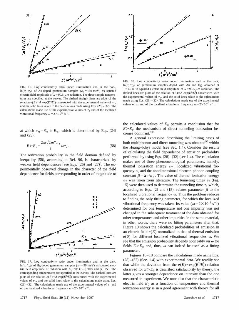
In strong electric fields, one observes transition to dirtunneling that does not involve phonons.108 As evident fromFig. 12, photoconductive signals in strong fields are less texpected in the case of multiphonon tunneling ionizatioThis is seen also from Figs. 16–18, where ln(si /sd) is plot-ted as a function of squared electric fieldE for Ge:Au andGe:Hg for different wavelengths and temperatures. For fiein excess ofE0 the ionization probability grows slower withincreasingE than that in the multiphonon tunneling region
As shown in Sec. 1, multiphonon tunneling in an electfield gives only a correction to multiphonon-assisted thermemission. The emission probability proportionalexp(E2/Ec
2) was obtained taking into account the fact that telectron tunneling energy«m ~21! is less than the optimumdefect-tunneling energyE0 ~13!. The electron tunneling energy grows with electric field, thus reducingE0 . The mul-tiphonon tunneling approximation becomes invalid when«m
becomes equal toE0 . The critical value of the electric field
n.
in
-
1716Ganichev et al.
-
of
ity
ely,
ngy
d
notfor
rial,at.in
g
qs.e
eoneisticalall
s
,at
sal
at which «m5E0 is E0 , which is determined by Eqs.~24!and ~25!:
E@E052vA2m* «T
evt2 . ~58!
The ionization probability in the field domain defined byinequality ~58!, according to Ref. 96, is characterized byweaker field dependences@see Eqs.~26! and ~27!#. The ex-perimentally observed change in the character of the fiedependence for fields corresponding in order of magnitude
FIG. 16. Log conductivity ratio under illumination and in the dark,ln(si /sd), of Au-doped germanium samples («T5150 meV) vs squaredelectric field amplitude ofl590.5mm radiation. The three sample tempera-tures are specified at the curves. The dashed straight lines are plots ofrelatione(E)}A exp(E2/Ec
2) constructed with the experimental values oft2 ,and the solid lines relate to the calculations made using Eqs.~28!–~32!. Thecalculations made use of the experimental values oft2 and of the localizedvibrational frequencyv5231013 s21.
FIG. 17. Log conductivity ratio under illumination and in the dark,ln(si /sd), of Hg-doped germanium samples («T590 meV) vs squared elec-tric field amplitude of radiation withl~mm!: ~1–3! 90.5 and~4! 250. Thecorresponding temperatures are specified at the curves. The dashed lineplots of the relatione(E)}A exp(E2/Ec
2) constructed with the experimentalvalues oft2 , and the solid lines relate to the calculations made using Eq~28!–~32!. The calculations made use of the experimental values oft2 andof the localized vibrational frequencyv5231013 s21.
1717 Phys. Solid State 39 (11), November 1997
ldto
the calculated values ofE0 permits a conclusion that forE@E0 the mechanism of direct tunneling ionization becomes dominant.108
A general expression describing the limiting casesboth multiphonon and direct tunneling was obtained90 withinthe Huang–Rhys model~see Sec. 1.4!. Consider the resultsof calculating the field dependence of emission probabilperformed by using Eqs.~28!–~32! ~see 1.4!. The calculationmakes use of three phenomenological parameters, namthermal ionization energy«T , localized vibrational fre-quencyv, and the nondimensional electron-phonon coupliconstantb5D«/«T . The value of thermal ionization energ«T was taken from literature. The tunneling timest2 ~Fig.15! were then used to determine the tunneling timet1 which,according to Eqs.~2! and ~15!, relates parameterb to thelocalized vibrational frequencyv. Thus the problem reducesto finding the only fitting parameter, for which the localizevibrational frequency was taken. Its value (v5231013 s21)determined for one temperature and one impurity waschanged in the subsequent treatment of the data obtainedother temperatures and other impurities in the same matein other words, there were no fitting parameters after thFigure 19 shows the calculated probabilities of emissionan electric fielde(E) normalized to that of thermal emissione(0) for different localized vibrational frequenciesv. Wesee that the emission probability depends noticeably onv forfields E.E0 and, thus,v can indeed be used as a fittinparameter.
Figures 16–18 compare the calculations made using E~28!–~32! ~Sec. 1.4! with experimental data. We readily sethat while the deviation from thee(E)}exp(E2/Ec
2) relationobserved forE.E0 is described satisfactorily by theory, thlatter gives a stronger dependence on intensity than themeasured in experiment. We note also that the characterelectric field E0 as a function of temperature and thermionization energy is in a good agreement with theory for
the
are
s.
FIG. 18. Log conductivity ratio under illumination and in the darkln(si /sd), of germanium samples doped with Au and Hg, obtainedT546 K vs squared electric field amplitude ofl590.5mm radiation. Thedashed lines are plots of the relatione(E)}A exp(E2/Ec
2) constructed withthe experimental values oft2 , and the solid lines relate to the calculationmade using Eqs.~28!–~32!. The calculations made use of the experimentvalues oft2 and of the localized vibrational frequencyv5231013 s21.
1717Ganichev et al.

u
sh
no
o
s
n
li
nt
c
n
n
l
a,
ed
,
s
the studied impurities exhibiting weak electron-phonon copling.
One of the reasons for the discrepancy between theoand experiment in the high electric-field domain may be thscattering of tunneling carriers under the barrier, which sean upper bound for the tunneling probability. This proceswas considered for carrier tunneling through Schottkbarriers,117 where the observed tunneling probability waalso smaller than that predicted by theory. The energy of ttunneling electron«m and the length of the under-barriertunneling trajectory increase with electric field to the extewhere the scattering processes place a limit on the emissi
4.3. Charge effect and the Poole–Frenkel effect
In the region of relatively weak electric fields one alsobserves deviations from the exp(E2/EC
2) behavior, clearlyseen in Fig. 20 displaying the ln(si /sd) vs E2 relation forGe:Hg. The dominant mechanism in this ionization proceis the Poole–Frenkel effect~see Sec. 1.5!, which is seen inthe onset of an exponential dependence of photoresposignal on the square root of electric field,e(E)}expAE/EPF. Data for the weak-field region are shown inFigs. 21 and 22, where ln(si /sd) is plotted as a function ofthe square root of the high-frequency electric-field amptude,AE. In the low-field domain, the ionization probabilityis seen to grow strongly with decreasing temperature, following closely thee(E)}expAE/EPF relation. The square-rootdependence of ln(si /sd) on E and its temperature behaviorare in good agreement with Eqs.~33! and~34! describing thePoole–Frenkel effect.
At the same time the theory of Frenkel does not providan adequate description of the dependence of conductivitythe high-frequency electric field. The slope of the depedence of ln(si /sd) on the square root of electric field is abouone half that calculated from Eqs.~33! and~34!, which mayalso may be considered as an argument for the presencemultiphonon processes~Sec. 1.5!. For low fields, the conduc-
FIG. 19. Log probability ratio of ionization in an electric field to thermaionization, ln@e(E)/e(0)#, for Hg-doped germanium («T590 meV) vssquared electric-field amplitude calculated for different localized vibrationfrequencies forT577 K using Eqs.~28!–~32!. v(1013 s21): 1—6, 2—4,3—3.
1718 Phys. Solid State 39 (11), November 1997
-
ryetssy
e
tn.
s
se
-
-
eon-
of
tivity does not vary at all~Fig. 22!. The same deviationsfrom Eqs.~33! and ~34! are observed also in the case of dfields83 and accord with published data.83,118–122
The charge effect manifests itself also in multiphonotunneling ionization, resulting, according to Eq.~36!, in anadditional factor in the ionization probability. This is see
lFIG. 20. Log conductivity ratio under illumination and in the darkln(si /sd), of Hg-doped germanium samplesvs squared electric-field ampli-tude ofl590.5mm radiation. The corresponding temperatures are specifiat the curves.
FIG. 21. Log conductivity ratio under illumination and in the darkln(si /sd), of Hg-doped germanium samplesvs square root of the electric-field amplitude ofl590.5mm radiation. The corresponding temperatureare specified at the curves.
1718Ganichev et al.

thric
e
el-
onreis
the, i
ob
iswth
ce
he
ra-the
nal
a-
gve-see
t
di-
n-
g
n-c-is
ningal-atheas
k,
av
,
f
from extrapolation of the straight lines corresponding toregion of multiphonon tunneling ionization to zero electfield. We see that ln(si /sd) does not vanish forE50 ~Figs.12 and 20!, which implies thats i is not equal tosd , as thisfollowed from Eq.~23! which does not take into account thcharge effect.
4.4. Effects due to the high-frequency of FIR radiation
As shown in the preceding Sections, ionization of deimpurity centers by FIR-SBM radiation is a result of tunneing processes occurring in the wave electric field. The iization probability here does not depend on radiation fquency, and the action of the high-frequency fieldequivalent to application of a strong electric field acrosssample. As pointed out in Sec. 1.6, however, an increasradiation frequency or decrease of sample temperaturetransition to the conditionVt25V(\/2kBT1t1).1, shouldresult in the ionization probability becoming dependentfrequency. The frequency dependence of ionization probaity was measured in Ge:Hg samples («T590 meV).
The results obtained atT540 K and at wavelengthsfrom 35 to 280mm are presented graphically in Fig. 23. Itseen that the photoresponse signal grows substantiallyradiation frequency while retaining at the same timecharacter of the field dependence ln(si /sd)}exp(E2/Ec
2). Thesame sample does not exhibit any frequency dependenhigher frequencies~Fig. 9!.
FIG. 22. Log conductivity ratio under illumination and in the darln(si /sd), of Hg-doped germanium samples at 77 Kvs square root of theradiation electric-field amplitude. The data are presented for different wlengths of the exciting radiation.l~mm!: ~1! 90.5, ~2! 250.
1719 Phys. Solid State 39 (11), November 1997
e
p
--
ein.e.
nil-
ithe
at
Experiments showed that within this frequency range tln(si /sd)}exp(E2/Ec
2) relation, which is typical of mul-tiphonon tunneling, occurs above 30 K. For lower tempetures, the frequency dependence becomes stronger, andelectric field dependence of the photoresponse sigchanges its character.
The field dependence of the ionization probability mesured for Ge:Hg within the temperature rangeT535280 Kand at wavelengthsl5352280mm was used to derive theeffective tunneling timet2* ~see Sec. 1.6!. Figure 24 displaysthe dependence of the ratiot2* /t2 , wheret2 is the tunnelingtime in a dc electric field, as a function of parameterVt2
which is dominant in the frequency effects. The tunnelintime t2 was derived from measurements at the longest walengths, where no frequency dependence is observed. Wethat t2* 5t2 up to Vt.1, in support of the conclusion thathe radiation field acts in this region as a dc field~all theexperiments quoted here before were done with this contion met!. An increase ofVt2 , which corresponds to anincrease of frequency or decrease of temperature@see Eq.~12!#, brings about a substantial increase in the effective tuneling time compared to the tunneling timet2 . Figure 24presents also thet2* /t2 ratio as a function ofVt2 calculatedusing Eq.~56!. The theory of multiphonon-assisted tunnelin~Sec. 1! is seen to agree well with experimental data.
As already pointed out, the theory of multiphonon tuneling in dc and high-frequency fields is valid provided eletron tunneling contributes little to thermal emission. Thistrue if the electron tunneling energy«m is much smaller thanthe energy of defect tunneling,E0 , and that of thermal ion-ization,«T . At low temperatures this condition breaks dowbecause of the smallness of the optimum defect-tunnelenergy, and, hence, the existing theory is inapplicableready for very low electric fields. Presented in Fig. 25 iscalculated dependence of the boundary beyond whichtheory of multiphonon tunneling energy is no longer valid,determined by the conditionE0 /«m51, on electric field
e-
FIG. 23. Log conductivity ratio under illumination and in the darkln(si /sd), of Hg-doped germanium samplesvs squared electric-field ampli-tude ofl590.5mm radiation obtained at 40 K for different wavelengths oexciting radiation~specified at the curves!. The straight lines plot relatione(E)}A exp(E2/Ec
2) with Ec2 used as a fitting parameter.
1719Ganichev et al.

ont
forccb
tyl
e
he
redm
Te-
reby
an50o-
ednal
thatgth
in
ulse26laserredtec-
na
.
g
:Te
strengthE, temperatureT, and radiation frequencyV forGe:Hg.5. KINETIC STUDIES OF THE LONG-LIVED COULOMBEXCITED STATES OF A SHALLOW IMPURITY CENTER
Development of sources capable of generating shFIR-SBM pulses permitted study of the dynamics of noequilibrium processes in semiconductors and semiconducquantum-well structures.21,40,123–126
In the case of interest to us here, using short pulsesthe ionization of impurities also makes possible the usetunneling ionization in the FIR-SBM field to study carrietrapping by impurities. As pointed out in Sec. 2, the kinetiof the photoresponse observed are in agreement with theture cross sections by an impurity which were obtainedother techniques for the materials under study.
Studies of the kinetics of the extrinsic photoconductivioccurring under multiphonon tunneling ionization of a shalow donor center~tellurium! in GaP in an electric field ofpulsed laser radiation in the FIR range revealed specific f
FIG. 24. Ratio of effective tunneling time,t2* , to tunneling time in a dcfield, t2 , vs Vt2 , obtained from the field dependence of the ionizatioprobability, which was determined for Ge:Hg in the temperature intervT535280 K and wavelength rangel5352280mm. l~mm!: ~1! 35, ~2!76, ~3! 90.5, ~4! 148, and~5! 280. The solid line is constructed using Eq~56!.
FIG. 25. Calculated boundary of applicability of multiphonon tunnelintheory determined from conditionE0 /«m51 vs electric field amplitudeE,temperatureT, and radiation frequencyV for Ge:Hg.
1720 Phys. Solid State 39 (11), November 1997
rt-or
orf
sap-y
-
a-
tures in the kinetics of carrier trapping and buildup in tvalley-orbit split 1s(E) state of the shallow donor level.127
Such long-lived excited electronic states were discoveearlier in simple substitutional impurities in Ge and Si fromodulation of the microwave absorption128,129
We also consider here carrier buildup in the excitedlevel in GaP under ionization of the impurity by short FIRSBM pulses.
5.1. Experimental investigation of the trapping kinetics intoshallow donor states of Te in GaP
Submillimeter photoconductivity measurements wecarried out on GaP samples, which were doped heavilytellurium to concentrations of 331017 and 731017 cm23
and lightly compensated. The samples were maintained inoptical cryostat with the temperature variable from 20 to 1K, where most of the carriers at thermal equilibrium are frzen out onto the ground-state impurity.
Illumination of a sample by FIR-SBM pulses increasits conductivity. Measurements of the photoresponse sigvswavelength, radiation intensity, and temperature showthe ionization probability does not depend on wavelenand grows nonlinearly with the electric fieldE of the radia-tion as exp(E2/Ec
2) while the characteristic fieldEc2 decreases
with decreasing temperature asT3, which implies that theionization is produced by multiphonon-assisted tunnelingthe electric field of the laser radiation.127
Figures 26 and 27 present typical photoresponse pshapes obtained in different time intervals. Shown in Fig.is the photoresponse of the sample measured during thepulse and immediately after its completion, to be compawith the laser pump pulse registered by a photon-drag de
l
FIG. 26. Oscillographic trace of the photoresponse signal from a GaPsample atT550 K ~upper curve! and of the exciting pulse withl590.5mmrecorded with a phonon-drag detector~lower curve!. The smooth curve forthe time intervalt.t0 is obtained using Eq.~64! with two fitting parameters,1/td15107 s21 and 1/td252.43103 s21.
1720Ganichev et al.

rr
v
-e
cthinr
n
b
-h
ss
inr
asr
rthtb
o
o
cen-of
f
isightate.e ofand
ran-m-cayws
rly,nalbe-
is-ex-er-vedby
mb
cay
ef theon-
tor. The first fast photoresponse component is clippeddemonstrate more clearly the unusual behavior of thesponse after the radiation pulse. The response is seen to gduring the radiation pulse and subsequently drop to zerotimes shorter than 40 ns. After the end of the pulse, howe~for t.t0!, the signal starts to grow again and reachesmaximum in one microsecond, to finally fall off exponentially to zero~Fig. 27!. The signal growth after the end of thpulse can be fitted well by the functiona@12exp((t2t0)/tr)#,with a characteristic timet r of the order of 1027 s. Thecharacteristic time of the subsequent slow exponential det1 does not depend on the intensity and frequency ofradiation but is strongly temperature dependent, increasby nearly three orders of magnitude with the temperatudecreasing from 150 K (6ms) to 35 K ~3 ms!. Figure 28presents the reciprocal decay time, 1/t1 , as a function ofinverse temperature. This strong temperature dependencebe well fitted in a first approximation by the functio1/t151/t0 exp(2D«/kT) with D«528 meV.
The fast component of the signal is accounted forionization and fast capture into the excited Coulomb statestellurium.130,131The main difficulty consists here in explaining the growth and decay of the signal after the end of tradiation pulse.
The heating of the electron gas or of the sample awhole can be excluded as possible formation mechanismthe photoconductive signal. It was shown132,133that at 70 Kand higher the electron mobility and, hence, conductivityGaP decreases with increasing temperature. Thus obsetion of positive photoconductivity excludes electron gheating by radiation as a possible cause of the photosponse. Besides, heating of the sample cannot account focomplex time behavior of the slow signal component anddetected increase of the exponential decay time constanthree orders of magnitude with the temperature changingfive times only.
Presence of additional deep impurities, for instance,oxygen, which has a small capture cross section~10222 cm2,Ref. 134! cannot explain the observed kinetics of the photresponse signal. To obtain the measured long decay time
FIG. 27. Oscillographic trace of a photoresponse signal obtained fromGa:P sample atT530 K. The smooth curve for the time intervalt.t0 isobtained using Eq.~64! with two fitting parameters, 1/td15107 s21 and1/td252.53102 s21.
1721 Phys. Solid State 39 (11), November 1997
toe-owinera
ayege
can
yof
e
aof
va-
e-theebyy
f
-by
this mechanism, one would have to assume that the contration of oxygen in the sample is comparable to thattellurium, 531017 cm23, which contradicts the low level olight compensation in the material under study.
5.2. Kinetic model of the relaxation process in the presenceof a long-lived excited state
The initial fast decay of the photoconductive signaldue to the fast cascade trapping of free carriers into hexcited states, which subsequently relax to the ground sThe latter stage requires essentially a longer time becausthe large energy gap between the excited Coulomb statesthe ground state. In the case of deep centers1! it usually oc-curs through multiphonon-assisted processes or optical tsitions. The dynamic time consists in this case of two coponents, namely, a fast and a slower one. The slow detime is, however, either temperature-independent or growith temperature, which is at odds with experiment.75 Thusthe cascade trapping model, unless it is modified propecannot account for the increase of the photoconductive sigafter the end of the pulse, and the observed temperaturehavior of the slow signal decay.
We are going to show that the assumption of the extence of a long-lived excited state characterized by antremely small transition probability to the ground state pmits one to describe adequately the kinetics of the obsersignal. The carriers build up in this state and return laterthermal activation to an array of closely spaced Coulo
a
FIG. 28. Temperature behavior of the reciprocal photoconductivity-detime, 1/t1 , in GaP:Te. The curve plots 1/t151/t0@exp(2D«/kT)11.443102]s21 and D«528 meV. The insets show schematically thcamel-back structure of the conduction band and the energy position oground and of a number of the lowest excited states of Te in GaP cstructed in accordance with Ref. 135~bottom left corner!, and the kinaticmodel of relaxation~top right corner!.
1721Ganichev et al.

states located near the bottom of the conduction band, thusan
cp
eswhe
ic
th
thnehe
e
np
tictic
b-rora
ates
tio
In these conditions, concentrationn2 determines the concen-ntingto
e
26thenet-
ceneal.e:
dlyre.
ood
al
d
increasing the carrier concentration in the conduction baccordingly.
The inset to Fig. 28 shows a characteristic camel-bashaped structure of the conduction-band bottom and thesition of the ground state and of a number of the lowexcited states of Te in GaP, constructed in accordanceRef. 135. We readily see that valley-orbit coupling splits t1s state in GaP into two states@1s(E) and 1s(A)# separatedby a gap of 40.7 meV. Cascade trapping was shown75 tooccur primarily over thes states by one-phonon acousttransitions. Since the energy gap between the 1s(E) and theground state exceeds by far the maximum energy ofacoustic phonon~31.5 meV, Ref. 135! while being less thanthat of the optical phonon~51 meV by Ref. 135!, the elec-trons promoted to the 1s(E) level cannot transfer to theground state by one-phonon processes, which results inbuildup in this level. The most probable relaxation chanfrom this state is one-phonon excitation into the next, higlying s state, 2s(A), separated from 1s(E) by 28 meV. Notethat the exponential dependence of the slow-decay timet1
on temperature is characterized by an energy of 28 mOne may thus conjecture that electrons build up in the 1s(E)state, are promoted by thermal excitation to the 2s(A) state,and transfer to the closely lyingp states through absorptioand emission of acoustical phonons, to relax finally via otical ~infrared! transitions to the ground state. The kinemodel based on these assumptions is presented schemain the upper right corner of Fig. 28.
For t.t0 , when there is no generation of nonequilirium carriers, the rate equations determining the electconcentrationsn in the conduction band and the concenttionsn2 andnE in the 2s(A) and 1s(E) states can be written
dn
dt52
n
tc21e2cn2,
dn2
dt5
n
tc22e2cn22
n2
t2E1eE2nE2
n2
t2A,
dnE
dt5
n2
t2E2eE2nE2
nE
tEA. ~59!
We have neglected here the thermal population of the stand introduced the following characteristic transition timtc2-from the conduction band to the 2s(A) level, t2E andt2A-from 2s(A) to the 1s(E) and 1s(A) level, respectively,andtEA-from the 1s(E) to 1s(A) level. The probabilities ofthe reverse processes,e2c and eE2 , are related through theprinciple of detailed balance to thetc2 andt2E times, respec-tively. For instance, for the transition probabilityeE2 , whichis essential for the model, we obtain
eE251
t2Eexp~2D«2E /kBT!, ~60!
whereD«2E is the energy separation between the 1s(E) and2s(A) levels.
The first of Eqs.~59! shows that fort.t0 ,tc2 a quasi-equilibrium sets in between the electrons in the conducband and those populating the 2s(A) state, i.e.n5e2ctc2n2 .
1722 Phys. Solid State 39 (11), November 1997
d
k-o-t
ith
e
eirlr
V.
-
ally
n-
es:
n
tration n of nonequilibrium free carriers in the conductioband and, thus, the photoresponse signal. Substitun5e2ctc2n2 in Eq. ~59! reduces the set of three equationsa set of the two latter equations fort.t0 . Then the electronconcentration in the 2s(A) state as a function of time can bwritten
n2~ t !51
S 1
td12
1
td2D H Fn2
~0!S 1
t2A1
1
t2E2
1
tEA
2e2c
t2E
~t2A1t2E! D2eE2nE~0!GexpS 2
~ t2t0!
td1D
1FeE2n2~0!
t2A
~t2A1t2E!1eE2•nE
~0!G3expS 2
~ t2t0!
td2D J , ~61!
wheren2(0) and nE
(0) are the concentrations in states 2s(A)and 1s(E) at time t5t0 , respectively, andtd1 and td2 arethe dynamic relaxation times defined by
1
td15
1
t2A1
1
t2E1eE2
t2A
~t2A1t2E!, ~62!
1
td25eE2
t2E
~t2A1t2E!1
1
tEA~63!
Assumingt2E!t2A we come to the inequalitynE(0)@2
(0) . Ne-glecting in Eq.~61! terms proportional ton2
(0) compared tothose proportional tonE
(0) one obtains
n2~ t !'eE2nE
~0!
S 1
td12
1
td2D FexpS 2
~ t2t0!
td2D2expS 2
~ t2t0!
td1D G .
~64!
For td1,td2 , Eq. ~64! showsn2 to vary nonmonotonicallywith time, namely, after the removal of illuminationn2 ex-hibits a growth followed by an exponential decay. Figuresand 27 compare the evolution of carrier concentration inconduction band, which determines the photoresponse kiics and was calculated using Eq.~61!, with experiment. Thetimes td1 and td2 were taken as fitting parameters. Sinthese times differ by at least two orders of magnitude, oactually used only one fitting parameter in each time intervThe dynamic times determined in this way ar1/td15107 s21 and 1/[email protected] exp(D«2E /kBT)11.443102]s21(D«2E528 meV). Figure 28 presents calculatetd2 times~solid line! to be compared with the experimentaldetermined slow decay time as a function of temperatuThe results of a numerical calculation are seen to be in gagreement with experiment.
It can be shown that, within the temperature intervunder consideration, the last term in Eq.~62! is much smallerthan the sum of the first two terms, 1/t2A11/t2E . Neglect-ing it in Eq. ~62!, we find from the experimentally measuredynamic times and the temperature dependence oftd2 thethree characteristic times introduced earlier:t2E51027 s,
1722Ganichev et al.

t2A5531027 s, andtEA50.731022 s. These values ac-
dhenoond
taorv
uciaritinreoteasldonnieieonlduleteo
lincalinbi
enn
omnngityesndnsaratog
APPENDIX EFFECTS OF RADIATION HEATING
ethefreere-all.ansses
onin
eirasb,gef they
m-
ndue
e
, on
ofx-
ig-
tical
reoleon-
, aped
thetra-the
l ofa-
ns,as-on-by
cord with the conditiont2E,t2A!tEA used in the calcula-tion.
Thus investigation of the kinetics of FIR–SBM-inducephotoconductivity in GaP:Te permitted observation of tbuildup of electrons in the excited state of a shallow dolevel in times up to a few milliseconds, and its identificatias a valley-orbit split 1s(E) state. Electrons are promotefrom this state by thermal excitation into the higher-lyingsand p states, with subsequent relaxation to the ground soccurring primarily by radiative transitions. The existenceradiative transitions was established here through obsetion of infrared luminescence.127
6. CONCLUSIONS
Photoionization of deep impurity centers in semicondtors stimulated by high-intensity submillimeter laser radtion having photon energies much smaller than the impuionization energy has been discovered and studied withbroad range of intensities, wavelengths, and temperatuand for a variety of impurities. A comprehensive comparisof experimental data with the theory of multiphonon-assisand direct deep-impurity ionization in an electric field hshown that terahertz radiation acts frequently like a dc fie
Within a broad electric-field range, the carrier emissiprobability can be described in terms of multiphonoassisted tunneling. Thermally activated emission of carrfrom the ground state to continuum is usually accompanby thermal excitation of the system followed by tunnelingthe defect from the configuration corresponding to a bouelectron state to that of an ionized impurity. Electric fieenhances defect tunneling by the electrons tunneling throthe barrier produced by the electronic potential and the etric field. This enhancement of carrier emission was detecfrom the photoconductive signal. The field dependencethis signal permitted one to determine the defect tunnetimes. The self-trapped character of the impurity centerbe established unambiguously by comparing the tunnetime with the reciprocal temperature multiplied by a comnation of universal constants~namely,\/2kBT!.
For relatively weak and very strong fields, the observprobability of ionization differs from that of multiphonotunneling. In the weak-field domain, the impurity ionizatiois produced by the Poole–Frenkel effect, which results frlowering the energy of thermal ionization of attractive ceters. In strong fields, ionization occurs by direct tunneliwithout thermal activation. The proposed method of impurionization by short FIR-SBM laser pulses permits contactlapplication of very strong electric fields to a sample athus, helps one to avoid problems associated with the oof avalanche breakdown, current pinching etc., whichfrequently encountered when operating with strong stelectric fields. The high sensitivity of the photoresponsefers a possibility of measurements over a broad field ranfrom very low intensities to tens of kV per cm.
1723 Phys. Solid State 39 (11), November 1997
r
tefa-
--yas,
nd
.
-rsd
fd
ghc-dfgng
-
d
-
s,eteicf-e,
Absorption of high-power FIR–SBM radiation by frecarriers results in a strong heating of the electron gas. Inexperiments considered here, there are practically nocarriers, which is a condition of weak absorption, and thefore the heating of the electron gas and of the lattice is smOur analysis would not, however, be complete withoutassessment of the possible contribution of heating proceto photoconductivity.
The variation of sample conductivity caused by electrgas heating under FIR illumination is due to the changethe mobility of the carriers as a result of the change in thenergy distribution. This process is well known and wthoroughly studied on a variety of materials, namely, InSGaAs, Ge, etc. If the free-carrier concentration is larenough, the heating process can be described in terms oelectron temperatureTe , whose variation is determined bthe absorption of radiation. In the FIR region, for\V!\v0 ,where\v0 is the optical phonon energy, the electron teperature is found from the balance equation:
aI\V5Pac~Te!1Popt~Te!, ~A1!
wherea is the coefficient of absorption by free carriers, aPac(Te) andPopt(Te) are, respectively, the energy losses dto scattering from acoustic and optical phonons~see, e.g.,Refs. 136–142!. The energy contribution determining thphotoconductive signal due to heating~both linear and non-linear! depends on the absorption of radiation and, hencethe free-carrier concentration.
If the heating is weak, the radiation-induced variationthe conductivity can be well approximated by a simple epression
Ds
s5
1
m
]m
]TeU
Te5T0
DTe , ~A2!
whereT0 is the lattice temperature.We readily see that the sign of the photoconductive s
nal is determined by that of the derivative]m/]Te . It is wellknown that this sign can be positive~for instance, if scatter-ing from charged impurities is dominant! or negative~in thecase where scattering occurs predominantly from acousphonons, optical phonons, etc.!.141,143
The main experiments of deep-impurity ionization weperformed using germanium samples. To reveal the rheating processes play in the submillimeter-range photocductivity observed in samples having deep impuritiesstudy was carried out of the electron gas heating in Ge dowith shallow impurities~Ga,Sb! at close to liquid-nitrogentemperature, where the impurities are ionized, i.e. underconditions most favorable for the heating. The concentions were chosen close to those of deep impurities insamples considered in this work.
Free-carrier heating in Ge in the temperature intervainterest results in negative photoconductivity, since the mjor part here is played by scattering by acoustic phonowhich brings about a decrease of the mobility with increing electron-gas temperature. The kinetics of the photocductivity caused by the free-carrier heating is dominated
1723Ganichev et al.

the short times of the free- carrier energy relaxation, which29 213
te
ci
in
ufnn
ezab
edtabeon
bytio
tkee
lsheh
tfa
illuthasluo-io
ao
iso
poiewt
oeo
~100 ns! radiation pulses having energies not in excess of a
sell-r-
emy
igh
. A
P
,
D.
V.
a,
F.ett.
ev.
i
k,W.
.l.
n,nd.
lie usually in the range 10 210 s. Accordingly, the sig-nals generated by electron heating either repeat the radiapulse in shape or exhibit a more complex behavior in timbut do not exceed in duration the nanosecond-range extion pulses.
Thus observation of positive photoconductivitysamples containing less than 531014 cm23 deep impuritiesat T.77 K during times longer than the radiation pulse dration exclude electron gas heating as a possible cause ophotoresponse. This is accounted for by the suppressioheating in samples doped primarily by deep impurities amaintained at sufficiently low temperatures by carrier freeout at the impurity and, hence, a practically completesence of absorption.
Note that the free-carrier concentration in AlxGa12xSband AlxGa12xAs samples in which DX centers were studiwas high enough for the heating effects to provide a substial contribution to photoresponse. The strong differencetween the relaxation times of the heating-induced photocductivity and of the photoconductivity due to the ionizatioof the DX centers permitted, however, easy separationthese contributions.
In the conditions of strong nonlinear carrier heatinghigh-intensity radiation one can observe also photoionizaof deep impurities with light of\V,«T in the course oflight-induced impact ionization, first discovered in InSb.34 Inthis case one detects, in addition to the prevailing fasmphotoresponse signals, positive photoconductivity, whosenetics are dominated by the nonequilibrium-carrier lifetimSince the carriers are heated here by the high-frequency fithe probability of the light-induced impact ionization faloff exponentially with increasing radiation frequency. Topposite frequency-dependence patterns of behavior exited by tunneling~multiphoton! and impact ionization permione to identify the processes. Thus the absence of thenegative component ofm photoconductivity in the positivephotoresponse signal observed under high-intensity FIRmination in samples having deep impurities, as well asindependence of probability on wavelength, or its decrewith the latter, gives us grounds for an unambiguous excsion of light-induced impact ionization from among the prcesses which could be responsible for the deep-impurityization discussed in the present work.
In conclusion, consider the possible effect of lattice heing. Similarly to the case of electron gas heating, heatingthe lattice by radiation should affect the conductivity. In thcase, the sign of the photoconductivity is determined by bthe variation of mobility~the carriers are ionized! and anincrease of carrier concentration in the band~the carriers arefrozen out at the impurity!. The kinetics of photoconductivityare dominated in this case by the slow cooling of the samas a whole~on a time scale substantially longer than micrseconds!. Observation in samples containing deep impuritof signals with characteristic times of the order of a femicroseconds and shorter gives one grounds to excludeheating of the sample as a whole as the cause of the phresponse. We also note that no lattice heating effects wobserved in the bulk semiconductors illuminated by sh
1724 Phys. Solid State 39 (11), November 1997
ion,
ta-
-theofd--
n--
n-
of
n
i-.ld,
ib-
st
-ee-
n-
t-f
th
le-s
heto-rert
mJ, even at high free-carrier concentrations~see, for in-stance, Refs. 39–41, 43, 114!.
The authors are grateful to Deutsche Forschungsgeschaft for support of the work and to V. I. Perel’ for numeous fruitful discussions.
*Present address: A. F. Ioffe Physicotechnical Institute, Russian Acadof Sciences, 194021 St. Petersburg, Russia.
1!Although tellurium is a donor center, its ground-state energy is farly h~90 meV!.
1T. Y. Chang and T. J. Bridges, Opt. Commun.1, 423 ~1970!.2Th. de Temple, inInfrared and Millimeter Waves, edited by K. J. Button,New York, Vol. 1, 129~1979!.
3L. R. Elias, J. Hu, and G. Ramian, Nucl. Instrum. Methods Phys. Res237, 203 ~1985!.
4L. R. Elias, G. Ramian, J. Hu, and A. Amir, Phys. Rev. Lett.57, 424~1986!.
5A. A. Andronov, in Infrared and Millimeter Waves, edited by K. J. But-ton, New York, Vol. 16, 150~1986!.
6L. E. Vorob’ev, F. I. Osokin, V. I. Stafeev, and V. N. Tulupenko, JETLett. 34, 118 ~1981!.
7V. I. Gavrilenko, V. N. Murzin, S. A. Stoklitski�, and A. P. Chebotarev,JETP Lett.35, 97 ~1982!.
8Yu. L. Ivanov and Yu. B. Vasil’ev, Pis’ma Zh. Tekh. Fiz.9, 613 ~1983!@Sov. Tech. Phys. Lett.9, 264 ~1983!#.
9Yu. A. Mityagin, V. N. Murzin, O. N. Stepanov, and S. A. StoklitskyPhys. Scr.49, 699 ~1994!.
10I. V. Altukhov, M. S. Kagan, and V. P. Sinis, Opt. Quantum Electron.23,S211~1991!.
11S. D. Ganichev, S. A. Emel’yanov, and I. D. Yaroshetski�, JETP Lett.35,368 ~1982!.
12F. Keilmann, Infrared Phys.31, 373 ~1991!.13W. Bohm, E. Ettlinger, and W. Prettl, Phys. Rev. Lett.47, 1198~1981!.14S. D. Ganichev, S. A. Emel’yanov, E. L. Ivchenko, E. Yu. Perlin, and I.
Yaroshetski�, JETP Lett.37, 568 ~1983!.15S. D. Ganichev, S. A. Emel’yanov, E. L. Ivchenko, E. Yu. Perlin, Ya.
Terent’ev, A. V. Fedorov, and I. D. Yaroshetski�, Zh. Eksp. Teor. Fiz.91,1233 ~1986! @Sov. Phys. JETP64, 729 ~1986!#.
16A. Avetissian, M. Hosek, and H. Minassian, Solid State Commun.60, 419~1986!.
17B. N. Murdin, C. R. Pidgeon, A. K. Kar, D. A. Jaroszynski, J. M. OrtegR. Prazeres, F. Glotin, and D. C. Hutchings, Opt. Mater.2, 89 ~1993!.
18P. S. S. Guimara˜es, B. J. Keay, J. P. Kaminski, S. J. Allen, Jr., P.Hopkins, A. C. Gossard, L. T. Florez, and J. P. Harbison, Phys. Rev. L70, 3792~1993!.
19B. Galdrikian, B. Birnir, and M. Sherwin, Phys. Lett. A203, 319 ~1995!.20C. R. Pidgeon, A. Vass, G. R. Allan, W. Prettl, and L. Eaves, Phys. R
Lett. 50, 1309~1983!.21E. V. Beregulin, S. D. Ganichev, K. Yu. Glukh, and I. D. Yaroshetsk�,
Fiz. Tekh. Poluprovodn.21, 1005~1987! @Sov. Phys. Semicond.21, 615~1987!#.
22S. P. Lov and A. J. Sievers, inTransport, Correlation, and StructuralDefects, edited by H. Fritzsche~World Scientific, Singapore, 1990!.
23G. Jungwirt, R. Kropf, and W. Prettl, Int. J. Infrared Millim. Waves12,729 ~1991!.
24R. Till and F. Keilmann, Phys. Rev. B44, 1554~1991!.25F. Keilmann and R. Till, Opt. Quantum Electron.23, S231~1991!.26F. Keilmann and R. Till, Semicond. Sci. Technol.7, 633 ~1992!.27M. Helm, T. Fromherz, B. N. Murdin, C. R. Pidgeon, K. K. Geerinc
N. J. Hovenyer, W. Th. Wenckebach, A. F. G. van der Meer, and P.van Amersfoort, Appl. Phys. Lett.63, 3315~1993!.
28K. Craig, C. L. Felix, J. N. Heyman, A. G. Markelz, M. S. Sherwin, K. LCampman, P. F. Hopkins, and A. C. Gossard, Semicond. Sci. Techno9,627 ~1994!.
29W. J. Li, B. D. McCombe, J. P. Kaminski, S. J. Allen, M. I. StockmaL. S. Muratov, L. N. Pandey, T. F. George, and W. J. Schaff, SemicoSci. Technol.9, 630 ~1994!.
30P. M. Valov, B. S. Ryvkin, I. D. Yaroshetski�, and I. N. Yassievich, Fiz.Tekh. Poluprovodn.5, 904 ~1971! @Sov. Phys. Semicond.5, 797 ~1971!#.
1724Ganichev et al.

31M. Weispfenning, I. Hoeser, W. Bo¨hm, W. Prettl, and E. Scho¨ll, Phys.Rev. Lett.55, 754 ~1985!.
et
.
.
m
n,
n,
C.
,
.
an
rd,ev
s.
h-
nt
G.
,
r,
r,
r,
r,
,
d
,
,
,
Fiz. 11, 46 ~1985! @Sov. Tech. Phys. Lett.11, 20 ~1985!#.64S. D. Ganichev, S. A. Emel’yanov, A. G. Pakhomov, Ya. V. Terent’ev,
d
.
-
s
.
,
nol.
h.
k
32J. Kaminski, J. Spector, W. Prettl, and M. Weispfenning, Appl. Phys. L52, 233 ~1988!.
33S. D. Ganichev, A. P. Dmitriev, S. A. Emel’yanov, Ya. V. Terent’ev, I. DYaroshetski�, and I. N. Yassievich, JETP Lett.40, 948 ~1984!.
34S. D. Ganichev, A. P. Dmitriev, S. A. Emel’yanov, Ya. V. Terent’ev, I. DYaroshetski�, and I. N. Yassievich, Zh. E´ ksp. Teor. Fiz.90, 445 ~1986!@Sov. Phys. JETP63, 256 ~1986!#.
35A. Schilz, L. Huber, W. Prettl, and J. Kaminski, Appl. Phys. Lett.60,2394 ~1992!.
36A. Mayer and F. Keilmann, Phys. Rev. B33, 6962~1986!.37W. W. Bewley, C. L. Felix, J. J. Plombon, M. S. Sherwin, M. Sundara
P. F. Hopkins, and A. C. Gossard, Phys. Rev. B48, 2376~1993!.38M. Holthaus and D. W. Hone, Phys. Rev. B49, 16605~1994!.39S. D. Ganichev, S. A. Emel’yanov, and I. D. Yaroshetski�, JETP Lett.38,
448 ~1983!.40E. V. Beregulin, S. D. Ganichev, K. Yu. Glukh, G. M. Gusev, Z. D. Kvo
M. Yu. Martisov, A. Ya. Shik, and I. D. Yaroshetski�, JETP Lett.48, 269~1988!.
41E. V. Beregulin, S. D. Ganichev, K. Yu. Glukh, G. M. Gusev, Z. D. KvoA. Ya. Shik, and I. D. Yaroshetski�, Zh. Eksp. Teor. Fiz.97, 2012~1990!@Sov. Phys. JETP70, 1138~1990!#.
42J. Cerne, A. G. Markelz, M. S. Sherwin, S. J. Allen, M. Sundaram, A.Gossard, P. C. van Son, and D. Bimberg, Phys. Rev. B51, 5253~1995!.
43I. N. Kotel’nikov, A. Ya. Shul’man, S. D. Ganichev, N. A. VarvaninB. Mayerhofer, and W. Prettl, Solid State Commun.97, 827 ~1996!.
44N. G. Asmar, J. Cˇ erne, A. G. Markelz, E. G. Gwinn, M. S. Sherwin, K. LCampman, and A. C. Gossard, Appl. Phys. Lett. B68, 829 ~1996!.
45A. A. Ignatov, E. Schomburg, K. F. Renk, W. Schatz, J. E. Palmier,F. Mollot, Ann. Physik3, 137 ~1994!.
46K. Unterrainer, B. J. Keay, M. C. Wanke, S. J. Allen, D. LeonaG. Medeiros-Ribeiro, U. Bhattacharya, and M. J. W. Rodwell, Phys. RLett. 76, 2973~1996!.
47M. F. Kimmitt, F. I. M. Hammouda, and A. M. A. Assar, Infrared Phy23, 63 ~1983!.
48S. D. Ganichev, S. A. Emel’yanov, and I. D. Yaroshetski�, Fiz. Tekh.Poluprovodn.17, 698 ~1983! @Sov. Phys. Semicond.17, 436 ~1983!#.
49S. D. Ganichev, S. A. Emel’yanov, Ya. V. Terent’ev, and I. D. Yarosetski�, Fiz. Tekh. Poluprovodn.18, 266 ~1984! @Sov. Phys. Semicond.18,164 ~1984!#.
50E. Garate, R. Cook, C. Shaughnessy, G. Boudreaux, and J. Walsh, IInfrared Millim. Waves7, 1827~1986!.
51M. F. Kimmitt, C. R. Pidgeon, D. A. Jaroszynski, R. J. Bakker, A. F.van der Meer, and D. Oepts, Int. J. Infrared Millim. Waves13, 1065~1992!.
52S. D. Ganichev, E. L. Ivchenko, R. Ya. Rasulov, I. D. Yaroshetski�, andB. Ya. Averbukh, Fiz. Tverd. Tela~St. Petersburg! 35, 198 ~1993! @Phys.Solid State35, 104 ~1993!#.
53G. M. Gusev, Z. D. Kvon, L. I. Magarill, A. M. Palkin, V. I. SozinovO. A. Shega�, and M. V. Entin, JETP Lett.46, 33 ~1987!.
54E. V. Beregulin, S. D. Ganichev, K. Yu. Glukh, Yu. B. Lyanda-Gelleand I. D. Yaroshetski�, Fiz. Tverd. Tela~Leningrad! 30, 730 ~1988! @Sov.Phys. Solid State30, 418 ~1988!#.
55E. V. Beregulin, S. D. Ganichev, K. Yu. Glukh, Yu. B. Lyanda-Gelleand I. D. Yaroshetski�, Fiz. Tverd. Tela~Leningrad! 31, 115 ~1989! @Sov.Phys. Solid State31, 63, ~1989!#.
56E. V. Beregulin, S. D. Ganichev, K. Yu. Glookh, Yu. B. Lyanda-Gelleand I. D. Yaroshetski�, Crystal Prop. Prepar.19, 327 ~1989!.
57E. V. Beregulin, S. D. Ganichev, K. Yu. Glukh, Yu. B. Lyanda-Gelleand I. D. Yaroshetski�, Fiz. Tverd. Tela~St. Petersburg! 35, 461 ~1993!@Phys. Solid State35, 238 ~1993!#.
58S. D. Ganichev, I. N. Kotel’nikov, N. A. Mordovets, A. Ya. Shul’manand I. D. Yaroshetski�, JETP Lett.44, 301 ~1986!.
59S. D. Ganichev, K. Yu. Glukh, N. A. Mordovets, A. Ya. Shul’man, anI. D. Yaroshetski�, Zh. Eksp. Teor. Fiz.102, 907~1992! @Sov. Phys. JETP75, 495 ~1992!#.
60I. N. Kotel’nikov, A. Ya. Shul’man, N. A. Mordovets, S. D. Ganichevand W. Prettl, J. Phys. Low-Dimens. Struct.12, 133 ~1995!.
61S. D. Ganichev, A. Ya. Shul’man, N. A. Mordovets, I. N. Kotel’nikovand W. Prettl, Int. J. Infrared Millim. Waves17, 1353~1996!.
62I. N. Kotel’nikov, A. Ya. Shul’man, N. A. Varvanin, S. D. GanichevB. Mayerhofer, and W. Prettl, JETP Lett.62, 48 ~1995!.
63S. D. Ganichev, Ya. V. Terent’ev, and I. D. Yaroshetski�, Pisma Zh. Tekh.
1725 Phys. Solid State 39 (11), November 1997
t.
,
d
.
. J.
and I. D. Yaroshetski�, Pisma Zh. Tekh. Fiz.11, 913 ~1985! @Sov. Tech.Phys. Lett.11, 377 ~1985!#.
65A. V. Andrianov, E. V. Beregulin, S. D. Ganichev, K. Yu. Glukh, anI. D. Yaroshetski�, Pisma Zh. Tekh. Fiz.14, 1326 ~1988! @Sov. Tech.Phys. Lett.14, 580 ~1988!#.
66S. D. Ganichev, K. Yu. Glukh, I. N. Kotel’nikov, N. A. Mordovets, A. YaShul’man, and I. D. Yaroshetski�, Pis’ma Zh. Tekh. Fiz.15, No. 8, 8~1989! @Sov. Tech. Phys. Lett.15, 582 ~1989!#.
67E. V. Beregulin, S. D. Ganichev, I. D. Yaroshetski�, P. T. Lang, W.Schatz, and K. F. Renk,Phys. Concepts of Materials for Novel OptoElectronic Device Applications II: Device Physics and Applications, Proc.SPIE1362, 853 ~1990!.
68E. V. Beregulin, S. D. Ganichev, and I. D. Yaroshetski�, Physical Con-cepts of Materials for Novel Opto-Electronic Device Applications II, ed-ited by F. Bertran and E. Gornik, Proc. SPIE1985, 523 ~1993!.
69S. D. Ganichev, W. Prettl, and P. G. Huggard, Phys. Rev. Lett.71, 3882~1993!.
70S. M. Ryvkin, Photoelectric Phenomena in Semiconductors@in Russian#,Fizmatgiz, Moscow, 1963.
71G. M. Martin and S. Makram-Ebeid, inDeep Centers in Semiconductor,edited by S. T. Pantelides~Gordon and Breach, N.Y., 1986!.
72N. T. Bagraev and V. A. Mashkov, Izv. Akad. Nauk SSSR, Ser. Fiz50,251 ~1986! @sic#.
73D. J. Chadi and K. J. Chang, Phys. Rev. B39, 10063~1989!.74P. M. Mooney, J. Appl. Phys.67, R1 ~1990!.75V. N. Abakumov, V. I. Perel, and I. N. Yassievich,Nonradiative Recom-
bination in Semiconductors, edited by V. M. Agranovich and A. A. Ma-radudin,Modern Problems in Condensed Matter Sciences, Vol. 33 ~North-Holland, Amsterdam, 1991!.
76P. M. Mooney and T. N. Theis, Comments Condens. Matter Phys.16, 167~1992!.
77R. C. Newman, Semicond. Sci. Technol.9, 1749~1994!.78K. Huang and A. Rhys, Proc. R. Soc. London, Ser. A204, 406 ~1950!.79C. H. Henry and D. V. Lang, Phys. Rev. B15, 989 ~1977!.80C. H. Henry and D. V. Lang, Phys. Rev. B15, 989 ~1975!.81T. Markvart, J. Phys. C17, 6303~1984!.82V. N. Abakumov, I. A. Merkulov, V. I. Perel’, and I. N. Yassievich, Zh
Eksp. Teor. Fiz.89, 1472~1985! @Sov. Phys. JETP62, 853 ~1985!#.83P. T. Landsberg,Recombination in Semiconductors~Cambridge Univer-
sity Press, New York, 1991!.84L. D. Landau and E. M. Lifshits,Quantum Mechanics~Pergamon Press
Oxford, 1974!.85R. Landauer and Th. Martin, Rev. Mod. Phys.66, 217 ~1994!.86S. D. Ganichev, I. N. Yassievich, and W. Prettl, Semicond. Sci. Tech
11, 679 ~1996!.87L. V. Keldysh, Zh. Eksp. Teor. Fiz.34, 994 ~1958! @Sov. Phys. JETP7,
685 ~1958!#.88S. Makram-Ebeid and M. Lannoo, Phys. Rev. B25, 6406~1982!.89V. Karpus and V. I. Perel’, JETP Lett.42, 497 ~1985!.90V. Karpus and V. I. Perel, Zh. E´ ksp. Teor. Fiz.91, 2319 ~1986! @Sov.
Phys. JETP64, 1376~1986!#.91A. F. Tasch, Jr., and C. T. Sah, Phys. Rev. B1, 800 ~1970!.92K. Irmscher, H. Klose, and K. Maass, Phys. Status Solidi A75, K25
~1983!.93V. Karpus, JETP Lett.44, 430 ~1986!.94J. Frenkel, Phys. Rev.54, 647 ~1938!.95V. N. Abakumov, V. Karpus, V. I. Perel’, and I. N. Yassievich, Fiz. Tek
Poluprovodn.22, 262 ~1988! @Sov. Phys. Semicond.22, 159 ~1988!#.96L. V. Keldysh, Zh. Eksp. Teor. Fiz.47, 1945~1964! @Sov. Phys. JETP20,
1307 ~1965!#.97Yu. A. Bychkov and A. M. Dykhne, Zh. E´ ksp. Teor. Fiz.58, 1734~1970!
@Sov. Phys. JETP31, 928 ~1970!#.98B. I. Ivlev and V. I. Mel’nikov, Zh. Eksp. Teor. Fiz.90, 2208 ~1986!
@Sov. Phys. JETP63, 1295~1986!#.99A. A. Vedenov, G. D. Myl’nikov, and D. N. Sobolenko, Usp. Fiz. Nau
138, 477 ~1982! @Sov. Phys. Usp.25, 833 ~1982!#.100M. Rosenbluth, R. J. Temkin, and K. J. Button, Appl. Opt.15, 2635
~1976!.101S. F. Dyubko and L. D. Fesenko,Tables of Lasing Lines of Optically-
Pumped Submillimeter Lasers@in Russian# ~Preprint IRE, Acad. Sci. Ukr.SSR, Kharkov, 1979!.
102O. J. E. Knight, NPL Report45, 200 ~1981!.
1725Ganichev et al.

103K. Gullberg, B. Hartmann, and B. Kleman, Phys. Scr.8, 177 ~1973!.104C. T. Gross, J. Kiess, A. Mayer, and F. Keilmann, IEEE J. Quantum
lm
cs
ys
nd
ttl
a
-
la
V
B
lz,
K. Campman, S. Farfad, P. F. Hopkins, and A. C. Gossard, Physica D83,229 ~1995!.
s,
ettl,
.
te
od-
Electron.QE-23, 377 ~1987!.105B. K. Meyer, G. Bischopink, K. W. Benz, A. Scha¨fner, and G. Pensl,
J. Cryst. Growth128, 475 ~1993!.106R. Krause-Rehberg, Th. Drost, A. Polity, G. Roos, G. Pensl, D. Vo
B. K. Meyer, G. Bischopink, and K. W. Benz, Phys. Rev. B48, 11723~1993!.
107R. J. Keyes,Optical and Infrared Detectors, Topics in Applied Physi~Springer, Berlin, 1980!.
108S. D. Ganichev, J. Diener, and W. Prettl, Solid State Commun.92, 883~1994!.
109S. D. Ganichev, J. Diener, I. N. Yassievich, and W. Prettl, EurophLett. 29, 315 ~1995!.
110S. D. Ganichev, I. N. Yassievich, W. Prettl, J. Diener, B. K. Meyer, aK. W. Benz, Phys. Rev. Lett.75, 1590~1995!.
111S. D. Ganichev, E. Ziemann, Th. Gleim, I. N. Yassievich, and W. PreVerh. Dtsch. Phys. Ges.5, 700 ~1997!.
112E. V. Buryak, S. A. Kaufman, and K. M. Kulikov, Fiz. Tverd. Tel~Leningrad! 5, 345 ~1963! @Sov. Phys. Solid State5, 249 ~1963!#.
113S. A. Kaufman, K. M. Kulikov, and N. P. Likhtman, Fiz. Tekh. Poluprovodn.4, 129 ~1970! @Sov. Phys. Semicond.4, 102 ~1970!#.
114S. D. Ganichev, S. A. Emel’yanov, and I. D. Yaroshetski�, Fiz. Tekh.Poluprovodn.21, 1011~1987! @Sov. Phys. Semicond.21, 618 ~1987!#.
115S. D. Ganichev, J. Diener, and W. Prettl, Appl. Phys. Lett.64, 1977~1994!.
116I. A. Merkulov, A. A. Pakhomov, and I. N. Yassievich, Fiz. Tverd. Te~Leningrad! 28, 2127~1986! @Sov. Phys. Solid State28, 1188~1986!#.
117R. Combescot and G. Schreder, J. Phys. C6, 1363~1973!.118T. Hirai and O. Nakada, J. Appl. Phys.7, 112 ~1968!.119M. Ieda, G. Sawa, and S. Kato, J. Appl. Phys.42, 3737~1971!.120G. A. N. Connell, D. L. Camphausen, and W. Paul, Philos. Mag.26, 541
~1972!.121D. Pai, J. Appl. Phys.46, 5122~1975!.122N. G. Zhdanova, M. S. Kagan, E. G. Landsberg, L. V. Levkin, and V.
Petrishchev, JETP Lett.62, 119 ~1995!.123R. H. M. Groeneveld and D. Grischovsky, JOSA B11, 1 ~1994!.124D. Grischovsky, S. Kelding, M. van Exter, and C. H. Fattinger, JOSA
7, 2006~1990!.125M. S. Sherwin, K. Craig, B. Galdrikian, J. N. Heyman, A. G. Marke
1726 Phys. Solid State 39 (11), November 1997
,
.
,
.
126B. N. Murdin, C. J. G. M. Langerak, M. Helm, P. Kruck, W. HeisV. Rosskopf, G. Strasser, E. Gornik, M. Du¨r, S. M. Goodnick, S. C. Lee,I. Galbraith, and C. R. Pidgeon, Superlattices Microstruct.19, 17 ~1996!.
127S. D. Ganichev, E. Zepezauer, W. Raab, I. N. Yassievich, and W. PrPhys. Rev. B55, 9243~1997!.
128I. V. Altukhov, Ya. E. Pokrovski�, O. I. Smirnova, and V. P. Sinis, FizTekh. Poluprovodn.24, 1134 ~1990! @Sov. Phys. Semicond.24, 450~1990!#.
129Ya. E. Pokrovskii, O. I. Smirnova, and N. A. Khvalkovskii, Solid StaCommun.93, 405 ~1995!.
130R. Z. Bachrach, P. D. Dapkus, and O. G. Lorimor, J. Appl. Phys.45,4971 ~1974!.
131A. N. Pikhtin, D. A. Yas’kov, and G. F. Glinski�, Fiz. Tverd. Tela~Len-ingrad! 12, 386 ~1970! @Sov. Phys. Solid State12, 307 ~1970!#.
132D. N. Nasledov, V. V. Negreskul, S. I. Radautsan, and S. V. Slobchikov, Phys. Status Solidi10, 37 ~1965!.
133H. C. Montgomery, J. Appl. Phys.39, 2002~1968!.134P. Dean, inDeep Centers in Semiconductors~Gordon and Breach, N.Y.,
1986!.135W. Scott, J. Appl. Phys.50, 472 ~1979!.136K. Seeger,Semiconductor Physics~Springer, Wien, 1973! @Russian
trans., Mir, Moscow, 1977#.137V. Denis and J. Pazhela,Hot Electrons@in Russian#, Mintis, Vilnjus,
1971.138Electrons in Semiconductors, edited by J. Pozhela,3, ~Mokslas, Vilnjus,
1981!.139M. Asche, Z. S. Gribnikov, V. V. Mitin, and O. G. Sarbe�, Hot Electrons
in Many-Valley Semiconductors@in Russian# Naukova Dumka, Kiev,1982.
140E. M. Conwell, High-Field Transport in Semiconductors~AcademicPress, New York, 1967! @Russian trans., Mir, Moscow, 1970!.
141I. N. Yassievich and I. D. Yaroshetski�, Fiz. Tekh. Poluprovodn.9, 857~1975! @Sov. Phys. Semicond.9, 565 ~1975!#.
142V. G. Agafonov, P. M. Valov, B. S. Ryvkin, and I. D. Yaroshetski�, Fiz.Tekh. Poluprovodn.9, 867~1975! @Sov. Phys. Semicond.9, 571~1975!#.
143J. B. Gunn, J. Phys. Chem. Solids8, 239 ~1959!.
Translated by G. Skrebtsov
1726Ganichev et al.