reversible electrical reduction and oxidation of graphene
TRANSCRIPT
EKIZ ET AL. VOL. 5 ’ NO. 4 ’ 2475–2482 ’ 2011
www.acsnano.org
2475
March 10, 2011
C 2011 American Chemical Society
Reversible Electrical Reduction andOxidation of Graphene OxideOkan €Oner Ekiz,* Mustafa Urel, Hasan G€uner, Alpay Koray Mizrak, and Aykutlu Dana*
UNAM-Institute of Materials Science and Nanotechnology, Bilkent University, 06800 Ankara, Turkey
Graphene1-3 has received tremen-dous attention in recent years dueto its potential applications in elec-
tronics,4-6 sensors,7-9 energy storage,10-12
and optics.13-15 Despite the extreme intrin-sic mobility of graphene,16 semimetallicelectronic band structure limited its use inhigh-performance transistors. Quantumconfinement effects were theoretically17,42
and experimentally18,19 shown to modifythe band structure, making graphene amore versatile material. Chemical modifica-tion is still being actively sought to formsemiconductors in the graphene family andimplement conventional optoelectronic de-vice structures. Novel devices have beenreported that combine the superior electro-nic properties of graphene with other che-mical and mechanical phenomena, such asresistive switching and electromechanicalmemories.20-22 The mechanism of ob-served resistive switching in some gra-phene-based devices remained unclear.Graphene oxide (GO) is an insulator with
a large effective band gap and band struc-ture that depends on the stoichiometry.23,24
It has been previously observed that gra-phene oxide can be reduced controllably atlow temperature (low-T) in ambient atmos-phere.25 In such a low-temperature reduc-tion process, the resistivity of the films canbe continuouslymonitored and can be usedto control the degree of reduction. Interrup-tion of thermal reduction results in partiallyreduced graphene oxide (PRGO). Conduc-tion mechanisms of such PRGO films areknown to be different than multilayer gra-phene (MLG) films, as evidenced by tem-perature dependence of resistivity.25-27 Ahopping transport mechanism was thoughtto be dominant in such films, and limitedevidence for the presence of oxygen-richdomains was provided through scanningtunneling microscopy (STM) imaging ofPRGO layers.28 Recently, thermal site-selec-tive reduction of graphene oxide is demons-tratedusingaheatedatomic forcemicroscope
tip.29 STM has also been used to imagehydrogen atoms on graphene and to createnanoscale heterostructure patterns by tip-induced hydrogen desorption.30 Recently(in an article published after the submissionof this work), a conductive atomic forcemicroscopy tip was used to characterizenanoscale surface conductivity of grapheneoxide, and tip-induced reduction wasshown to be possible.31
In this work, we demonstrate electricallyinduced reversible reduction of grapheneoxide, resulting in changes in the electronicand optical properties of graphene-basedthin films. It is observed that optical andelectronic property changes are correlatedwith the formation of a graphene/grapheneoxide nanomesh.
RESULTS
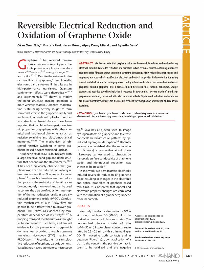
We study the electrical reduction of GO inair, using multilayer GO (MLGO) films de-posited on metalized glass substrates. Thetwo-terminal devices consist of thin(∼10-50 nm) Pd/Au planar contacts, sepa-rated by 0.3-0.6 mm, with a thin multilayerGO film covering both contacts and inbetween (Figure 1a). Upon application of abias to the contacts, the positive contact isseen to be oxidized and the negative
* Address correspodence [email protected],[email protected].
Received for review June 23, 2010and accepted March 10, 2011.
Published online10.1021/nn1014215
ABSTRACT We demonstrate that graphene oxide can be reversibly reduced and oxidized using
electrical stimulus. Controlled reduction and oxidation in two-terminal devices containing multilayer
graphene oxide films are shown to result in switching between partially reduced graphene oxide and
graphene, a process which modifies the electronic and optical properties. High-resolution tunneling
current and electrostatic force imaging reveal that graphene oxide islands are formed on multilayer
graphene, turning graphene into a self-assembled heterostructure random nanomesh. Charge
storage and resistive switching behavior is observed in two-terminal devices made of multilayer
graphene oxide films, correlated with electrochromic effects. Tip-induced reduction and oxidation
are also demonstrated. Results are discussed in terms of thermodynamics of oxidation and reduction
reactions.
KEYWORDS: graphene . graphene oxide . electrochemistry . electrochromism .electrostatic force microscopy . resistive switching . tip-induced oxidation
ARTIC
LE
EKIZ ET AL. VOL. 5 ’ NO. 4 ’ 2475–2482 ’ 2011
www.acsnano.org
2476
contact is seen to be reduced. There is a potential dropbetween the contacts due to the finite conductivity ofthe films. The stoichiometry is observed to depend onthe distance from the contacts, as confirmed by X-rayphotoelectron spectroscopy (XPS) (Figure 1b). Thereduction/oxidation can be reversed by reversal ofbias. The optical transparencies of the films are alsodependent on the oxidation state. Wavelength-depen-dent linear transmission is measured using a fiber-coupled spectrometer near one of the contacts, whilethe bias is swept quasi-statically between -2.5 and2.5 V. A gradual increase of the absorption edge as afunction of applied bias is observed (Figure 2a). Theoptical transparency is correlated with the oxidationstate (Figure 2b,c), films being semitransparent in theoxidized state. During cyclic voltage sweeps, it isobserved that electrically induced oxidation/reductiontakes placewith time scales on the order of seconds forapplied bias voltages of(2.5 V. We infer the thicknessof the films to be 30-60 nm using optical measure-ments, assuming the films have absorption coefficientssimilar to graphene during the absorbing (reduced)state.32
We inspect the surface electronic properties of thetwo-terminal devices with an atomic force microscope(AFM), imaging the surface topography and conduc-tivity before and after voltage pulses applied betweenits terminals. Two-terminal devices are subjected tovoltage pulses (typically 2 to 3 V) while the tip isretracted. After the electrical reduction (or oxidation)process, the device contacts are grounded and the
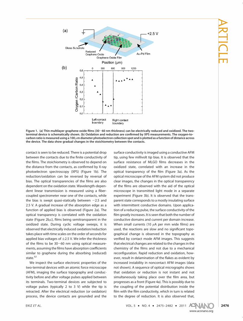
surface conductivity is imaged using a conductive AFMtip, using few millivolt tip bias. It is observed that thesurface resistance of MLGO films decreases in theoxidized state, correlated with an increase in theoptical transparency of the film (Figure 3a). As theoptical microscope of the AFM system did not produceclear images, the changes in the optical transparencyof the films are observed with the aid of the opticalmicroscope in transmitted light mode in a separateexperiment (Figure 3b). It is observed that the trans-parent state corresponds to amostly insulating surfacewith intermittent conductive domains. Upon applica-tion of a reducing pulse, the surface conductivity of thefilm greatly increases. It is seen that both the number ofconductive domains and current per domain increase.When small currents (10 μA per mm wide films) areused, the reactions are slow and no significant topo-graphical change is observed in the topography asverified by contact mode AFM images. This suggeststhat electrical changes are related to the changes in thechemistry of the films and not due to a mechanicalreconfiguration. Rapid reduction and oxidation, how-ever, result in delamination of the flakes as evident byincreased instability in noncontact AFM images (datanot shown). A sequence of optical micrographs showsthat oxidation or reduction is not instant and notsimultaneously taking place over the film area, butprogresses as a front (Figure 4a). This is possibly due tothe coupling of the potential distribution inside thefilm with the film conductivity, which in turn is relatedto the degree of reduction. It is also observed that,
Figure 1. (a) Thin multilayer graphene oxide films (30-60 nm thickness) can be electrically reduced and oxidized. The two-terminal device is schematically shown. (b) Oxidation and reduction are confirmed by XPS measurements. The oxygen-to-carbon ratio ismeasuredusing a 100μmdiameter photoelectron collection spot and is plotted as a function of distance acrossthe device. The data show gradual changes in the stoichiometry between the contacts.
ARTIC
LE

EKIZ ET AL. VOL. 5 ’ NO. 4 ’ 2475–2482 ’ 2011
www.acsnano.org
2477
when low (< ( 2 V) maximum bias values are used,reversible optical and resistive switching continue formultiple cycles (about 20 in our devices) before the filmshows an irreversible reduction in electrical resistance.Our observations suggest that previously observedresistive switching in graphene oxide and graphenedevices is a result of chemical modification of gra-phene due to reversible binding of oxygen.22,23 Thedrop-cast films consist of a large number of flakes. Thethickness and conductivity of the films are not veryuniform, and we attribute the device failure to forma-tion of highly conductive dendrite-like shorting paths,
which are observable in optical images (Figure 4b). Asthe shorting paths are formed, current paths andvoltage distributions inside the film change in a waythat the bias needed for the reduction/oxidation pro-cess cannot be sustained uniformly and controllably atall parts of the film (see Supporting Information).We also investigate film surfaces in various oxidation
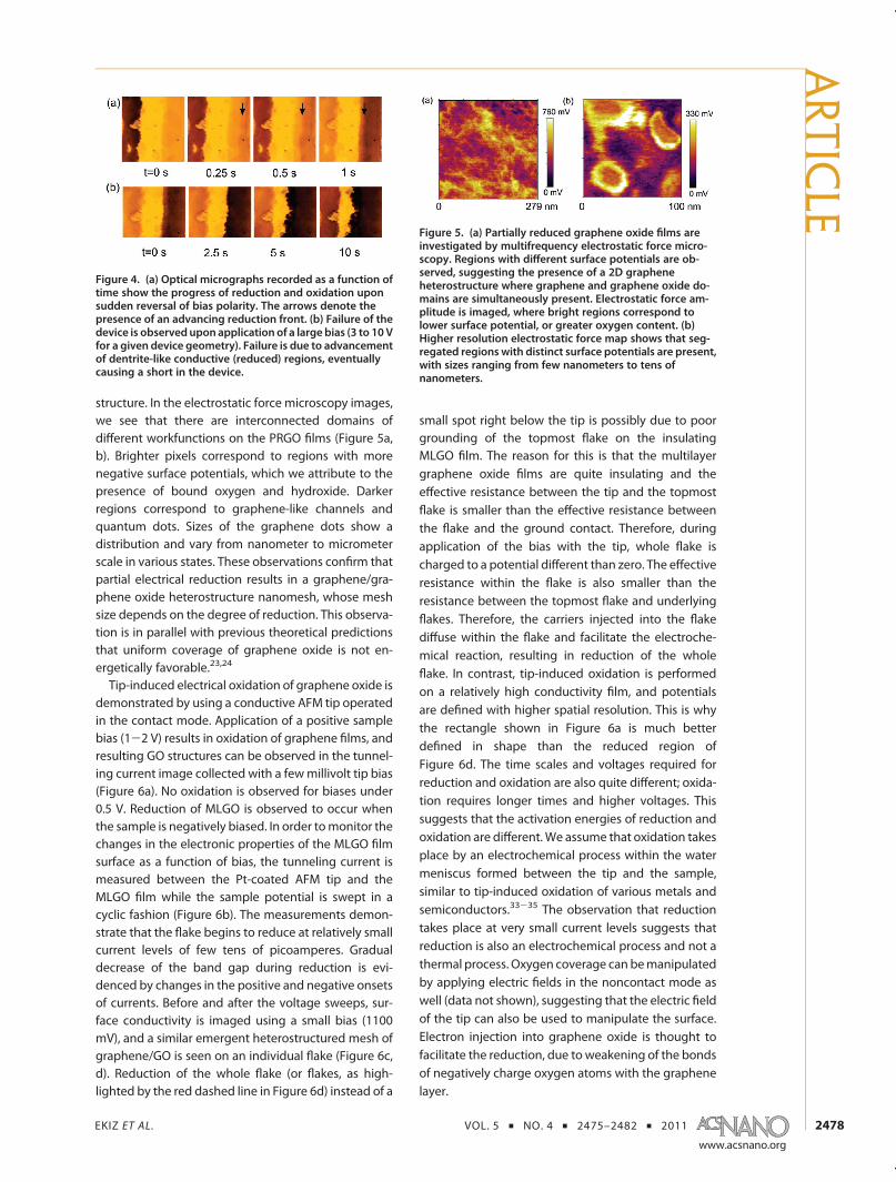
states using high-resolution multifrequency electro-static forcemicroscopy. Since electrostatic forcemicro-scopy is a noncontact and relatively nondestructivemeasurement technique, we use it as a reliable com-plementary way of confirming the surface electronic
Figure 3. (a) Tunneling current images showing the effect of reversible electrical oxidation and reduction in three consecutivevoltage cycles (þ2 V, -2 V, þ2 V for tens of seconds). The images are collected at the same location, by grounding the twocontacts and applying a ∼10 mV tip bias. The surface conductivity is observed to switch in reduced and oxidized states.(b) Representative optical micrographs (observed by bright-field transmitted light, scale bar 30 μm) of multilayer grapheneoxide films show spatially uniform transmission at the beginning of the bias cycles (left), where reduced transmission isobserved upon application of bias that reduces the left side of the film (middle, minus sign, dark region). The opticaltransmission can be manipulated by reversing the polarity of applied bias and causing the left side to oxidize and theright side to reduce (right).
Figure 2. (a) Linear optical transmission of the films is measured using a 25 μm core fiber optic light collector near one of thecontactswhile the bias is swept between-2.5 and 2.5 V. It is observed thatwavelength-dependent transmission is adjustableby applying an external bias. Representative XPS spectra that correspond to the (b) reduced and (c) oxidized states show thecorrelation of optical transparency with stoichiometry.
ARTIC
LE
EKIZ ET AL. VOL. 5 ’ NO. 4 ’ 2475–2482 ’ 2011
www.acsnano.org
2478
structure. In the electrostatic force microscopy images,we see that there are interconnected domains ofdifferent workfunctions on the PRGO films (Figure 5a,b). Brighter pixels correspond to regions with morenegative surface potentials, which we attribute to thepresence of bound oxygen and hydroxide. Darkerregions correspond to graphene-like channels andquantum dots. Sizes of the graphene dots show adistribution and vary from nanometer to micrometerscale in various states. These observations confirm thatpartial electrical reduction results in a graphene/gra-phene oxide heterostructure nanomesh, whose meshsize depends on the degree of reduction. This observa-tion is in parallel with previous theoretical predictionsthat uniform coverage of graphene oxide is not en-ergetically favorable.23,24
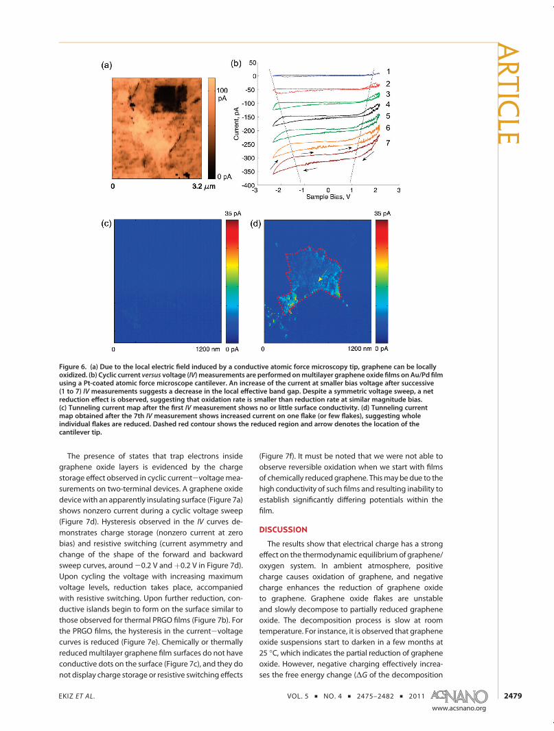
Tip-induced electrical oxidation of graphene oxide isdemonstrated by using a conductive AFM tip operatedin the contact mode. Application of a positive samplebias (1-2 V) results in oxidation of graphene films, andresulting GO structures can be observed in the tunnel-ing current image collected with a fewmillivolt tip bias(Figure 6a). No oxidation is observed for biases under0.5 V. Reduction of MLGO is observed to occur whenthe sample is negatively biased. In order tomonitor thechanges in the electronic properties of the MLGO filmsurface as a function of bias, the tunneling current ismeasured between the Pt-coated AFM tip and theMLGO film while the sample potential is swept in acyclic fashion (Figure 6b). The measurements demon-strate that the flake begins to reduce at relatively smallcurrent levels of few tens of picoamperes. Gradualdecrease of the band gap during reduction is evi-denced by changes in the positive and negative onsetsof currents. Before and after the voltage sweeps, sur-face conductivity is imaged using a small bias (1100mV), and a similar emergent heterostructured mesh ofgraphene/GO is seen on an individual flake (Figure 6c,d). Reduction of the whole flake (or flakes, as high-lighted by the red dashed line in Figure 6d) instead of a
small spot right below the tip is possibly due to poorgrounding of the topmost flake on the insulatingMLGO film. The reason for this is that the multilayergraphene oxide films are quite insulating and theeffective resistance between the tip and the topmostflake is smaller than the effective resistance betweenthe flake and the ground contact. Therefore, duringapplication of the bias with the tip, whole flake ischarged to a potential different than zero. The effectiveresistance within the flake is also smaller than theresistance between the topmost flake and underlyingflakes. Therefore, the carriers injected into the flakediffuse within the flake and facilitate the electroche-mical reaction, resulting in reduction of the wholeflake. In contrast, tip-induced oxidation is performedon a relatively high conductivity film, and potentialsare defined with higher spatial resolution. This is whythe rectangle shown in Figure 6a is much betterdefined in shape than the reduced region ofFigure 6d. The time scales and voltages required forreduction and oxidation are also quite different; oxida-tion requires longer times and higher voltages. Thissuggests that the activation energies of reduction andoxidation are different. We assume that oxidation takesplace by an electrochemical process within the watermeniscus formed between the tip and the sample,similar to tip-induced oxidation of various metals andsemiconductors.33-35 The observation that reductiontakes place at very small current levels suggests thatreduction is also an electrochemical process and not athermal process. Oxygen coverage can bemanipulatedby applying electric fields in the noncontact mode aswell (data not shown), suggesting that the electric fieldof the tip can also be used to manipulate the surface.Electron injection into graphene oxide is thought tofacilitate the reduction, due to weakening of the bondsof negatively charge oxygen atoms with the graphenelayer.
Figure 4. (a) Optical micrographs recorded as a function oftime show the progress of reduction and oxidation uponsudden reversal of bias polarity. The arrows denote thepresence of an advancing reduction front. (b) Failure of thedevice is observedupon application of a large bias (3 to 10 Vfor a given device geometry). Failure is due to advancementof dentrite-like conductive (reduced) regions, eventuallycausing a short in the device.
Figure 5. (a) Partially reduced graphene oxide films areinvestigated by multifrequency electrostatic force micro-scopy. Regions with different surface potentials are ob-served, suggesting the presence of a 2D grapheneheterostructure where graphene and graphene oxide do-mains are simultaneously present. Electrostatic force am-plitude is imaged, where bright regions correspond tolower surface potential, or greater oxygen content. (b)Higher resolution electrostatic force map shows that seg-regated regions with distinct surface potentials are present,with sizes ranging from few nanometers to tens ofnanometers.
ARTIC
LE
EKIZ ET AL. VOL. 5 ’ NO. 4 ’ 2475–2482 ’ 2011
www.acsnano.org
2479
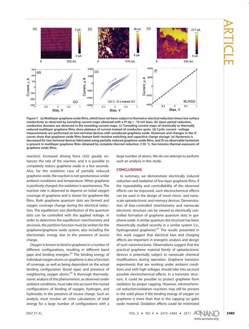
The presence of states that trap electrons insidegraphene oxide layers is evidenced by the chargestorage effect observed in cyclic current-voltagemea-surements on two-terminal devices. A graphene oxidedevicewith an apparently insulating surface (Figure 7a)shows nonzero current during a cyclic voltage sweep(Figure 7d). Hysteresis observed in the IV curves de-monstrates charge storage (nonzero current at zerobias) and resistive switching (current asymmetry andchange of the shape of the forward and backwardsweep curves, around-0.2 V andþ0.2 V in Figure 7d).Upon cycling the voltage with increasing maximumvoltage levels, reduction takes place, accompaniedwith resistive switching. Upon further reduction, con-ductive islands begin to form on the surface similar tothose observed for thermal PRGO films (Figure 7b). Forthe PRGO films, the hysteresis in the current-voltagecurves is reduced (Figure 7e). Chemically or thermallyreducedmultilayer graphene film surfaces do not haveconductive dots on the surface (Figure 7c), and they donot display charge storage or resistive switching effects
(Figure 7f). It must be noted that we were not able toobserve reversible oxidation when we start with filmsof chemically reducedgraphene. Thismaybe due to thehigh conductivity of such films and resulting inability toestablish significantly differing potentials within thefilm.
DISCUSSION
The results show that electrical charge has a strongeffect on the thermodynamic equilibriumof graphene/oxygen system. In ambient atmosphere, positivecharge causes oxidation of graphene, and negativecharge enhances the reduction of graphene oxideto graphene. Graphene oxide flakes are unstableand slowly decompose to partially reduced grapheneoxide. The decomposition process is slow at roomtemperature. For instance, it is observed that grapheneoxide suspensions start to darken in a few months at25 �C, which indicates the partial reduction of grapheneoxide. However, negative charging effectively increa-ses the free energy change (ΔG of the decomposition
Figure 6. (a) Due to the local electric field induced by a conductive atomic force microscopy tip, graphene can be locallyoxidized. (b) Cyclic current versus voltage (IV) measurements are performed onmultilayer graphene oxide films on Au/Pd filmusing a Pt-coated atomic force microscope cantilever. An increase of the current at smaller bias voltage after successive(1 to 7) IV measurements suggests a decrease in the local effective band gap. Despite a symmetric voltage sweep, a netreduction effect is observed, suggesting that oxidation rate is smaller than reduction rate at similar magnitude bias.(c) Tunneling current map after the first IV measurement shows no or little surface conductivity. (d) Tunneling currentmap obtained after the 7th IV measurement shows increased current on one flake (or few flakes), suggesting wholeindividual flakes are reduced. Dashed red contour shows the reduced region and arrow denotes the location of thecantilever tip.
ARTIC
LE
EKIZ ET AL. VOL. 5 ’ NO. 4 ’ 2475–2482 ’ 2011
www.acsnano.org
2480
reaction). Increased driving force (ΔG) greatly en-hances the rate of the reaction, and it is possible tocompletely reduce graphene oxide in a few seconds.Also, for the oxidation case of partially reducedgraphene oxide, the reaction is not spontaneous underambient conditions and temperature. When grapheneis positively charged, the oxidation is spontaneous. Thereaction rate is observed to depend on initial oxygencoverage of graphene and is slower for graphene-likefilms. Both graphene quantum dots are formed andoxygen coverage change during the electrical reduc-tion. The equilibrium size distribution of the quantumdots can be controlled with the applied voltage. Inorder to determine the equilibrium stoichiometry andstructure, the partition functionmust bewritten for thegraphene/graphene oxide system, also including theelectrostatic energy due to the presence of excesscharge.Oxygen is known to bind to graphene in a number of
different configurations, resulting in different bandgaps and binding energies.23 The binding energy ofindividual oxygen atoms on graphene is also a functionof coverage, as well as being dependent on the actualbinding configuration (bond type) and presence ofneighboring oxygen atoms.24 A thorough thermody-namic analysis of the phenomenon, as observed underambient conditions, must take into account themyriadconfigurations of binding of oxygen, hydrogen, andhydroxide, in the presence of excess charge. Such ananalysis must involve ab initio calculations of totalenergy for a large number of configurations with a
large number of atoms. We do not attempt to performsuch an analysis in this study.
CONCLUSIONS
In summary, we demonstrate electrically inducedreduction and oxidation of few-layer graphene films. Ifthe repeatability and controllability of the observedeffects can be improved, such electrochemical effectscan be used in the design of novel micro- and nano-scale optoelectronic andmemory devices. Demonstra-tion of bias-controlled stoichiometry and nanoscaleelectronic structure can be viewed as electrically con-trolled formation of graphene quantum dots in gra-phene oxide. A similar quantum dot structure has beentheoretically studied recently in a similar system (i.e.,hydrogenated graphene).41 The results presented inthis work suggest that electrical bias and chargingeffects are important in energetic analysis and designof such nanostructures. Observations suggest that thepractical graphene material family of optoelectronicdevices is potentially subject to nanoscale chemicalmodifications during operation. Graphene transistorexperiments that are working under ambient condi-tions and with high voltages should take into accountpossible electrochemical effects. In a transistor struc-ture, it could be possible to protect graphene fromoxidation by proper capping. However, electrochemi-cal reduction/oxidation reactions may still be presentin the solid phase if the binding energy of oxygen ongraphene is more than that in the capping (or gate)oxide material. Oxidation effects could be minimized
Figure 7. (a)Multilayer grapheneoxidefilms,which have not been subject to thermal or electical reduction shows low surfaceconductivity as observed by tunneling current maps obtained with a Pt tip (∼10 mV bias). (b) Upon partial reduction,conductive domains are observed in the tunneling current maps. (c) Tunneling current maps of chemically or thermallyreduced multilayer graphene films show plateaus of current instead of conductive spots. (d) Cyclic current-voltagemeasurements are performed on two-terminal devices with unreduced graphene oxide. Hysteresis and changes in the IVcurves show that graphene oxide films feature both resistive switching and capacitive charge storage. (e) Hysteresis isdecreased for two-terminal devices fabricated using partially reduced graphene oxide films, and (f) no observable hysteresisis present in multilayer graphene films obtained by complete thermal reduction (150 �C, few minutes thermal exposure) ofgraphene oxide films.
ARTIC
LE

EKIZ ET AL. VOL. 5 ’ NO. 4 ’ 2475–2482 ’ 2011
www.acsnano.org
2481
by use of a dielectric that does not contain oxygen,such as MgF2. Charge-induced chemical reactionscould also affect performance of graphene-based
energy storage devices such as supercapacitors. Thefindings show the importance of electrochemical ef-fects for graphene-based devices.
METHODSGraphene oxide was synthesized from natural graphite (SP-1,
Bay Carbon) by the Hummersmethod.36 Graphite oxide powder(0.75 g) was suspended in 50 mL of DI water and sonicated for30 min. The suspension was sequentially centrifuged at 8000and 14 500 rpm for 30 min each, to completely eliminateunexfoliated graphene oxide particles.Stable graphene suspensions were prepared by a fast and
simple method. Hydrazine hydrate (0.1 mL, Merck) was addedto the 10 mL of graphene oxide/water, and the mixture washeated to 85 �C for 1 h. A few minutes after the addition ofhydrazine hydrate, the color of themixture became black. At theend of 1 h, the graphene particles precipitated because ofaggregation. Acetone (Sigma-Aldrich) was added to the solu-tion with the same volume. After hydrazine treatment, thegraphene surface contained hydrazone groups.37 Acetone couldmodify the surface graphene by reacting with hydrazone groups;therefore, addition of acetone dissolves graphene in the waterand hydrazine hydrate mixture. To completely suspend aggre-gated graphene, 5 min of sonication was applied to the mixture.Two-terminal devices were fabricated by sputtering Au-Pd
films on precleaned glass substrates by using a 300 μm wideshadow mask. Graphene or GO suspensions were drop-castedon the devices fabricated. The films were dried under vacuum.Devices were characterized using a digital source meter(Keithley 2700) with a probe station. Graphene devices wereannealed at 125-150 �C for 30 s beforemeasurements. Partiallyreduced graphene oxide samples were prepared by thermalannealing of graphene oxide films at 125 �C for 30 s. Thermalannealing processes were applied on a preheated hot plate.Electrochemical experiments were performed under ambientconditions in clean room conditions, at room temperature(T = 25 ( 0.5 �C) and 40 ( 5% humidity as monitored by ahumidity sensor, under 1 atm pressure.Electrical and XPS (X-ray photoelectron spectroscopy) mea-
surements were done on a Thermo K-Alpha system.Multifrequency electrostatic force microscopy was imple-
mented using modified commercial silicon cantilevers withspring constants of 2-4 N/m, and resonance frequencies of65-75 kHz. The tips are double-stage electron-beam-induceddeposited Pt tips with a tip radius of 2-5 nm as inspected byscanning electron microscopy. Low-frequency electrostatic exci-tation was applied at 5 kHz, and first and second time harmonicsof the electrostatic forcesweremonitored using lock-in amplifiers(Stanford Research Systems, SR 830). The details of the high-resolution multifrequency electrostatic force microscopy andspectroscopy can be found in references 38-40.
Acknowledgment. This work was partially supported byTUBITAK under grant 107T547 and the State PlanningOrganiza-tion of Republic of Turkey, project UNAM. Authors thank M.Guler for critical reading of the manuscript, and S. Ciraci fordiscussions on graphene.
Supporting Information Available: Video micrographs, cap-tured in bright-field transmitted light microscopy mode, de-monstrating electrochromic effects, dentritic domain forma-tion, and failure of two-terminal graphene oxide film devicesupon application of various voltage pulses. This material isavailable free of charge via the Internet at http://pubs.acs.org.
REFERENCES AND NOTES1. Novoselov, K. S.; Geim, A. K.; Morozov, S. V.; Jiang, D.;
Katsnelson, M. I.; Grigorieva, I. V.; Dubonos, S. V.; Firsov,A. A. Two-Dimensional Gas of Massless Dirac Fermions inGraphene. Nature 2005, 438, 197–200.
2. Geim, A. K.; Novoselov, K. S. The Rise of Graphene. Nat.Mater. 2007, 6, 183–191.
3. Stankovich, S.; Dikin, D. A.; Dommett, G. H. B.; Kohlhaas,K. M.; Zimney, E. J.; Stach, E. A.; Piner, R. D.; Nguyen, S. T.;Ruoff, R. S. Graphene-Based Composite Materials. Nature2006, 442, 282–286.
4. Meric, I.; Han, M. Y.; Young, A. F.; Ozyilmaz, B.; Kim, P.;Shepard, K. L. Current Saturation in Zero-Bandgap, Top-Gated Graphene Field-Effect Transistors. Nat. Nanotech-nol. 2008, 3, 654–659.
5. Lin, Y. M.; Dimitrakopoulos, C.; Jenkins, K. A.; Farmer, D. B.;Chiu, H. Y.; Grill, A.; Avouris, P. 100-GHz Transistors fromWafer-Scale Epitaxial Graphene. Science 2010, 327, 662.
6. Novoselov, K. S.; Jiang, Z.; Zhang, Y.; Morozov, S. V.;Stormer, H. L.; Zeitler, U.; Maan, J. C.; Boebinger, G. S.;Kim, P.; Geim, A. K. Room-Temperature Quantum HallEffect in Graphene. Science 2007, 315, 1379.
7. Schedin, F.; Geim, A. K.; Morozov, S. V.; Hill, E. W.; Blake, P.;Katsnelson, M. I.; Novoselov, K. S. Detection of IndividualGas Molecules Adsorbed on Graphene. Nat. Mater. 2007,6, 652–655.
8. Wehling, T. O.; Novoselov, K. S.; Morozov, S. V.; Vdovin, E. E.;Katsnelson, M. I.; Geim, A. K.; Lichtenstein, A. I. MolecularDoping of Graphene. Nano Lett. 2008, 8, 173–177.
9. Robinson, J. T.; Perkins, F. K.; Snow, E. S.; Wei, Z.; Sheehan,P. E. Reduced Graphene Oxide Molecular Sensors. NanoLett. 2008, 8, 3137–3140.
10. Stoller, M. D.; Park, S.; Zhu, Y.; An, J.; Ruoff, R. S. Graphene-Based Ultracapacitors. Nano Lett. 2008, 8, 3498–3502.
11. Yoo, E.; Kim, J.; Hosono, E.; Zhou, H.; Kudo, T.; Honma, I.Large Reversible Li Storage of Graphene NanosheetFamilies for Use in Rechargeable Lithium Ion Batteries.Nano Lett. 2008, 8, 2277–2282.
12. Wang, L.; Lee, K.; Sun, Y.; Lucking, M.; Chen, Z.; Zhao, J. J.;Zhang, S. B. Graphene Oxide as an Ideal Substrate forHydrogen Storage. ACS Nano 2009, 3, 2995–3000.
13. Mueller, T.; Xia, F.; Avouris, P. Graphene Photodetectors forHigh-Speed Optical Communications. Nat. Photonics2010, 4, 297–301.
14. Gokus, T.; Nair, R. R.; Bonetti, A.; Bohmler, M.; Lombardo, A.;Novoselov, K. S.; Geim, A. K.; Ferrari, A. C.; Hartschuh, A.Making Graphene Luminescent by Oxygen Plasma Treat-ment. ACS Nano 2009, 3, 3963–3968.
15. Sun, Z.; Hasan, T.; Torrisi, F.; Popa, D.; Privitera, G.; Wang, F.;Bonaccorso, F.; Basko, D. M.; Ferrari, A. C. Graphene Mode-Locked Ultrafast Laser. ACS Nano 2010, 4, 803–810.
16. Bolotina, K. I.; Sikesb, K. J.; Jianga, Z.; Klimac, M.; Fuden-berga, G.; Honec, J.; Kima, P.; Stormera, H. L. UltrahighElectron Mobility in Suspended Graphene. Solid StateCommun. 2008, 146, 351–355.
17. Sevincli, H.; Topsakal, M.; Ciraci Superlattice, S. Structuresof Graphene-Based Armchair Nanoribbons. Phys. Rev. B2008, 78, 245402.
18. Han, M. Y.; Ozyilmaz, B.; Zhang, Y.; Kim, P. Energy Band-Gap Engineering of Graphene Nanoribbons. Phys. Rev.Lett. 2007, 98, 206805.
19. Bai, J.; Zhong, X.; Jiang, S.; Huang, Y.; Duan, X. GrapheneNanomesh. Nat. Nanotechnol. 2010, 5, 190–194.
20. Li, Y.; Sinitskii, A.; Tour, J. M. Electronic Two-TerminalBistable Graphitic Memories. Nat. Mater. 2008, 7, 966–971.
21. He, C. L.; Zhuge, F.; Zhou, X. F.; Li, M.; Zhou, G. C.; Liu, Y. W.;Wang, J. Z.; Chen, B.; Su, W. J.; et al. Nonvolatile ResistiveSwitching in Graphene Oxide Thin Films. Appl. Phys. Lett.2009, 95, 232101.
22. Echtermeyer, T. J.; Lemme, M. C.; Baus, M.; Szafranek, B. N.;Geim, A. K.; Kurz, H. Nonvolatile Switching in Graphene
ARTIC
LE

EKIZ ET AL. VOL. 5 ’ NO. 4 ’ 2475–2482 ’ 2011
www.acsnano.org
2482
Field-Effect Devices. IEEE Electron Device Lett. 2008, 29,952–954.
23. Yan, J.; Xian, L.; Chou, M. Y. Structural and ElectronicProperties of Oxidized Graphene. Phys. Rev. Lett. 2009,103, 086802.
24. Boukhvalov, D. W.; Katsnelson, M. I. Modeling of GraphiteOxide. J. Am. Chem. Soc. 2008, 130, 10697–10701.
25. Jung, I.; Dikin, D. A.; Piner, R. D.; Ruoff, R. S. TunableElectrical Conductivity of Individual Graphene OxideSheets Reduced at Low Temperatures. Nano Lett. 2008,8, 4283–4287.
26. Lopez, V.; Sundaram, R. S.; Gomez-Navarro, C.; Olea, D.;Burghard, M.; Gomez-Herrero, J.; Zamora, F.; Kern, K.Chemical Vapor Deposition Repair of Graphene Oxide: ARoute to Highly-Conductive Graphene Monolayers. Adv.Mater. 2009, 21, 1–4.
27. Cote, L. J.; Cruz-Silva, R.; Huang, J. Flash Reduction andPatterning of Graphite Oxide and Its Polymer Composite.J. Am. Chem. Soc. 2009, 131, 11027–11032.
28. Gomez-Navarro, C.; Thomas Weitz, R.; Bittner, A. M.; Scolari,M.; Mews, A.; Burghard, M.; Kern, K. Electronic TransportProperties of Individual Chemically Reduced GrapheneOxide Sheets. Nano Lett. 2007, 7, 3499–3503.
29. Wei, Z.; Wang, D.; Kim, S.; Kim, S.; Hu, Y.; Yakes, M. K.;Laracuente, A. R.; Dai, Z.; Marder, S. R.; et al. NanoscaleTunable Reduction of Graphene Oxide for GrapheneElectronics. Science 2010, 328, 1373.
30. Sessi, P.; Guest, J. R.; Bode, M.; Guisinger, N. P. PatterningGraphene at the Nanometer Scale via Hydrogen Desorp-tion. Nano Lett. 2009, 9, 4343–4347.
31. Mativetsky, J. M.; Treossi, E.; Orgiu, E.; Melucci, M.; Veronese,G. P.; Samori, P.; Palermo, V. Local Current Mapping andPatterning of Reduced Graphene Oxide. J. Am. Chem. Soc.2010, 132, 14130–14136.
32. Nair, R. R.; Blake, P.; Grigorenko, A. N.; Novoselov, K. S.;Booth, T. J.; Stauber, T.; Peres, N. M. R.; Geim, A. K. FineStructure Constant Defines Visual Transparency of Gra-phene. Science 2008, 320, 1308.
33. Avouris, P.; Martel, R.; Hertel, T.; Sandstrom, R. AFM-Tip-Induced and Current-Induced Local Oxidation of Siliconand Metals. Appl. Phys. A: Mater. Sci. Process. 1998, 66,S659–S667.
34. Okada, Y.; Amano, S.; Kawabe, M.; Harris, J. S. BasicMechanisms of an Atomic Force Microscope Tip-InducedNano-oxidation Process of GaAs. J. Appl. Phys. 1998, 83,7998–8001.
35. Avouris, P.; Hertel, T.; Martel, R. Atomic Force MicroscopeTip-Induced Local Oxidation of Silicon: Kinetics, Mechan-ism and Nanofabrication. Appl. Phys. Lett. 1997, 71, 285–287.
36. Hummers, W. S.; Offeman, R. E. Preparation of GraphiticOxide. J. Am. Chem. Soc. 1958, 80, 1339.
37. Stankovich, S.; Piner, R. D.; Chen, X.; Wu, N.; Nguyen, S. T.;Ruoff, R. S. Stable Aqueous Dispersions of GraphiticNanoplatelets via the Reduction of Exfoliated GraphiteOxide in the Presence of Poly(sodium 4-styrenesulfonate).J. Mater. Chem. 2006, 16, 155–158.
38. Ding, X. D.; An, J.; Xu, J. B.; Li, C.; Zeng, R. Y. ImprovingLateral Resolution of Electrostatic Force Microscopy byMultifrequency Method under Ambient Conditions. Appl.Phys. Lett. 2009, 94, 223109.
39. Ziegler, D.; Reichen, J.; Naujoks, N.; Stemmer, A. Compen-sating Electrostatic Forces by Single-Scan Kelvin ProbeForce Microscopy. Nanotechnology 2007, 18, 225505.
40. Bostanci, U.; Abak, M. K.; Aktas-, O.; Dana, A NanoscaleCharging Hysteresis Measurement by MultifrequencyElectrostatic Force Spectroscopy. Appl. Phys. Lett. 2008,92, 093108.
41. Singh, A. K.; Penev, E. S.; Yakobson, B. I. Vacancy Clusters inGraphane as Quantum Dots. ACS Nano 2010, 4, 3510–3514.
42. Singh, A. K.; Yakobson, B. I. Electronics and Magnetism ofPatterned Graphene Nanoroads. Nano Lett. 2009, 9,1540–1543.
ARTIC
LE