reversible computing - zettaflops
TRANSCRIPT

Reversible ComputingReversible ComputingA Requirement forA Requirement for
Extreme SupercomputingExtreme Supercomputing
Dr. Michael P. Frank, Assistant Professor
Dept. of Electrical & Computer Eng.
FAMU-FSU College of Engineering
ECE Department Graduate Seminar
Thursday, September 2, 2004

10/13/2004 M. Frank, "Reversible Computing" 2
Abstract• The energy dissipated per switching event directly limits any digital
system’s performance per unit of power consumption.– E.g., typical logic node switching energy today = ~0.1 fJ.
→ A 1 MW machine could do “only” 100 PFLOPs. (assuming 105 logic ops/FLOP)
→ A 1 ZFLOPs machine in today’s tech. would require at least 10 GW!– This is the approximate electrical power consumption of Norway!
• Traditional “irreversible” switching mechanisms are subject to a relatively high minimum energy dissipation per signal transition event.– The practical limit for irreversible CMOS may be only ~1 order of magnitude
better than today’s technology.• And further, any possible irreversible technology is at best only ~2-4 orders of
magnitude better than today’s!– E.g., 1 ZFLOPs, terrestrially � at least ~40 MW (non-adiabatic)
• Circumventing all these bounds will require moving to increasingly reversible switching mechanisms and logic styles…– With long-term implications for computer architecture, programming
languages, and algorithm design…
• In this talk, we survey reversible computing principles.– We argue: Reversible computing needs to be more aggressively explored!

10/13/2004 M. Frank, "Reversible Computing" 3
Moore’s Law (Devices/IC)
1
10
100
1,000
10,000
100,000
1,000,000
10,000,000
100,000,000
1,000,000,000
1950 1960 1970 1980 1990 2000 2010
Avg. increase
of 57%/year
4004
8086286
386486DX Pentium
P2
P3P4
Itanium 2Madison
Early
Fairchild
ICs
Intel µpu’s

10/13/2004 M. Frank, "Reversible Computing" 4
ITRS '03 Feature Lengths
250
2232
4565
13090
180
350
0.1
1
10
100
1000
1990 1995 2000 2005 2010 2015 2020 2025 2030 2035 2040 2045
Year of Production
Feature length (nm)
DRAM hp
MPU M1 hp
poly hp
printed GL
physical GL
Node
EOTNaïve linear extrapolations
Effective gate oxide thickness
Based on ITRS ’97-03 roadmaps(1 µm)
Silicon atom
DNA/CNT radius
Protein molecule
Virus
Hydrogen atom
Device Size Scaling Trends

ITRS '97-'03 Gate Energy Trends
1.E-22
1.E-21
1.E-20
1.E-19
1.E-18
1.E-17
1.E-16
1.E-15
1.E-14
1995 2000 2005 2010 2015 2020 2025 2030 2035 2040 2045
Year
CVV/2 energy, J
LP min gate energy, aJ
HP min gate energy, aJ
100 k(300 K)
ln(2) k(300 K)
1 eV
k(300 K)
9065
4532
22
130180
250
Room-temperature 100 kT reliability limit
One electron volt
Room-temperature von Neumann - Landauer limit
Room-temperature kT thermal energy
Practical limit for CMOS?
Naïve linear extrapolation
Trend of Min. Transistor Switching Energy
fJ
aJ
zJ
Based on ITRS ’97-03 roadmaps
Node numbers
(nm DRAM hp)

10/13/2004 M. Frank, "Reversible Computing" 6
Important Energy Limits
• Near-term leakage-based limit for MOSFETs:– May be ~5 aJ, roughly 10× lower than today.
• 10× faster machines, ~4-8 years left on the clock
• Reliability-based limit on bit energies:– Roughly 100 kT ≈ 400 zJ, ~100× below now.
• 100× faster machines, ~8-15 years to go…
• Landauer limit on dissipation per bit erasure:– About 0.7 kT ≈ 3 zJ, ~10,000× below today.
• 10,000× faster machines, ~15-30 years left…
• No limit is known for reversible computing…– We need to investigate this alternative further.

10/13/2004 M. Frank, "Reversible Computing" 7
FET Energy Limit• A practical limit for all transistors based on the field effect principle.
– It’s probably not an absolutely unavoidable, fundamental limit.• However, it is probably the biggest barrier to further transistor scaling today.
• The limit arises from the following chain of considerations:– We require reduced energy dissipation per logic operation.
→ Want small ½CV2 logic node energy (normally dissipated when switching)
→ Want small node capacitance C → small transistor size (also for speed)
→ Need to lower switching voltage V, due to many factors:• Gate oxide breakdown, punch-through, also helps reduce CV2.
→ Reduced on-off ratio Ron/off = Ion/Ioff < eVq/kT (at room temperature)• Comes from Boltzmann (or Fermi-Dirac) distrib. of state occupancies near equil.
– Independent of materials! (Carbon nanotubes, nanowires, molecules, etc.)
→ Increased off-state current Ioff and power IoffV, given high-performance Ion.
→ Also, increased per-area leakage current due to gate oxide tunneling, etc.
→ Previous two both increase total per-device power consumption floor• Adds to total energy dissipated per logic gate, per clock cycle
• Eventually, the extra power dissipation from leakage overwhelms the power/performance reductions that we would gain by reducing CV2!– Beyond this point, further transistor scaling hurts us, rather than helping.
• Transistor scaling then halts, for all practical purposes!

10/13/2004 M. Frank, "Reversible Computing" 8
Mitigating MOSFET Limits• Reduce the portion of the ½CV2 node energy that gets dissipated
– Reversible computing with adiabatic circuits does this
• Reduce parasitic capacitances that contribute to logic node’s C– via silicon-on-insulator (SOI) devices, low-κ field dielectric materials, etc.
• Use high-κ gate dielectric materials →– Allows gate dielectrics to be thicker for a given capacitance/area
– Reduces tunneling leakage current though gate dielectric. Also:
– Avoids gate oxide breakdown → allows higher V
→ indirectly helps reduce off-state conduction.
• Use multi-gate structures (FinFET, surround-gate, etc.) to – reduce subthreshold slope s = V/(log Ron/off) to approach theoretical optimum,
• s = T/q = (kT/q ln 10)/decade = 60 mV/decade
• Use multi-threshold devices & power-management architectures to turn off inactive devices to suppress leakage in unused portions of the chip
– The remaining leakage in the active logic is still a big problem, however…
• Lower operating temperature to increase Vq/kT and thus IDS on-off ratio?– May also lead to problems with carrier concentration, cooling costs, etc.
– Conflicts with the high generalized temperature of high-frequency logic signals
• Consider devices using non-field-effect based switching principles: – Y-branch, quantum-dot, spintronic, superconducting, (electro)mechanical, etc.

10/13/2004 M. Frank, "Reversible Computing" 9
Reliability-Based Limit• A limit on signal (bit) energy.
• Applies to any mechanism for storing a bit whose operation is based on the latching principle, namely:– We have some physical entity whose state (e.g. its location) encodes a bit.
• E.g., could be a packet of electrons, or a mechanical rod
– If the bit is 1, the entity gets “pushed into” a particular state and held there by a potential energy difference (between there and not-there) of E.
• The entity sits in there at thermal equilibrium with its environment.
– A potential energy barrier is then raised in between the states, to “latch” the entity into place (if present).
• A transistor is turned off, or a mechanical latching mechanism is locked down
• The Boltzmann distribution implies that E > T log N = kT ln N, in order for the probability of incorrect storage to be less than 1/N.– For electrons (fermions), we must use the Fermi-Dirac distribution instead…
• But this gives virtually identical results for large N.
• When erasing a stored bit, typically we would dissipate the energy E.– However, this limit might be avoidable via special level-matching, quasi-
adiabatic erasure mechanisms, or non-equilibrium bit storage mechanisms.

10/13/2004 M. Frank, "Reversible Computing" 10
Numerical Example
• Example: Reliability factor of N=1027 (e.g., 1 error in a 109
gate processor running for ~3 years at 10 GHz)– The entropy associated with the per-op error probability is then:
log 1027 = 27 log 10 = 27 kB ln 10 ≈ 62 kB = 8.6×10⁻²² J/K
– Heat that must be output to a room-T (300 K) environment:kB (300 K) ln 1027 = 2.6×10⁻¹⁹ J (or 260 zJ, or 1.6 eV)
• Sounds small, but…
– If each gate dumped this energy @ a frequency of 10 GHz,
• the total power dissipated by an entire 109-gate processor is 26 W.
• Could have at most 4 such processors within a 100 W power budget!
– Maximum performance: 4×10²⁰ gate-cyles/sec.
• or 4 PFLOPS, if processors require ~100,000 logic ops on average to carry out 1 standard (double-precision) floating-point op
– a fairly typical figure for today’s well-optimized floating-point units
• Typical COTS microprocessors today have ~100× additional overhead,
– Leading to 40 TFLOPS max performance if using these same architectures
» A 40-TFLOP supercomputer (e.g. Blue Gene/L) burns ~200 kW today
» Only 2,000× above the reliability-based limit!
10/13/2004 M. Frank, "Reversible Computing" 11
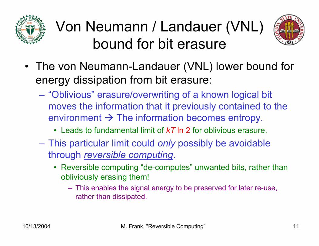
Von Neumann / Landauer (VNL)
bound for bit erasure
• The von Neumann-Landauer (VNL) lower bound for
energy dissipation from bit erasure:
– “Oblivious” erasure/overwriting of a known logical bit
moves the information that it previously contained to the
environment � The information becomes entropy.
• Leads to fundamental limit of kT ln 2 for oblivious erasure.
– This particular limit could only possibly be avoidable
through reversible computing.
• Reversible computing “de-computes” unwanted bits, rather than
obliviously erasing them!
– This enables the signal energy to be preserved for later re-use,
rather than dissipated.
10/13/2004 M. Frank, "Reversible Computing" 12
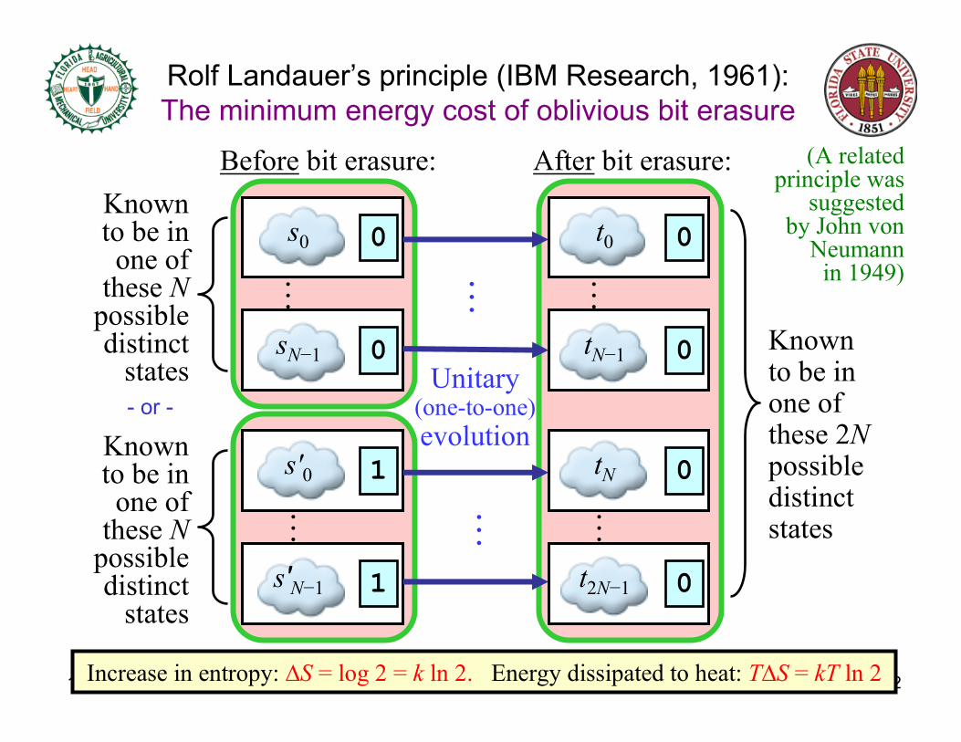
Rolf Landauer’s principle (IBM Research, 1961):
The minimum energy cost of oblivious bit erasure
…
Knownto be inone of
these Npossibledistinct
states
……
Knownto be inone ofthese 2Npossibledistinctstates
Unitary(one-to-one)
evolution
Before bit erasure: After bit erasure:
Increase in entropy: ∆S = log 2 = k ln 2. Energy dissipated to heat: T∆S = kT ln 2
0s0
0sN−1
…
1s′0
1s′N−1
…
…
0t0
0tN−1
0tN
0t2N−1
…
(A relatedprinciple was
suggestedby John von
Neumannin 1949)
- or -
Knownto be inone of
these Npossibledistinct
states
10/13/2004 M. Frank, "Reversible Computing" 13
Reversible Computing• A reversible digital logic operation is:
– Any operation that performs an invertible (one-to-one) transformation of the device’s local digital state space.
• Or at least, of that subset of states that are actually used in a design.
• Landauer’s principle only limits the energy dissipation of ordinary irreversible (many-to-one) logic operations.– Reversible logic operations could dissipate much less energy,
• Since they can be implemented in a thermodynamically reversible way.
• In 1973, Charles Bennett (IBM Research) showed how any desired computation can in fact be performed using only reversible logic operations (with essentially no bit erasure).– This opened up the possibility of a vastly more energy-efficient
alternative paradigm for digital computation.
• After 30 years of (sporadic) research, this idea is finally approaching the realm of practical implementability…– Making it happen is the goal of the RevComp project.

10/13/2004 M. Frank, "Reversible Computing" 14
Non-oblivious “erasure” (by decomputing known bits) avoids the von Neumann–Landauer bound
…
Npossibledistinct
states
Npossibledistinct
states
……
Npossibledistinctstates
Unitary(one-to-one)
evolution
Before decomputing B: After decomputing B:
Increase in entropy: ∆S → 0. Energy dissipated to heat: T∆S → 0
0s0
0sN−1
…
1s′0
1s′N−1
…
…
0t0
0tN−1
0t′0
0t′N−1
…
0
0
1
1
Npossibledistinctstates
0
0
1
1
A B
A B
A B
A B A B
A B
A B
A B
- or - - or -

10/13/2004 M. Frank, "Reversible Computing" 15
Adiabatic Circuits• Reversible logic can be implemented today using
fairly ordinary voltage-coded CMOS VLSI circuits.– With a few changes to the logic-gate/circuit architecture.
• We avoid dissipating most of the circuit node energy when switching, by transferring charges in a nearly adiabatic (literally, “without flow of heat”) fashion.– I.e., asymptotically thermodynamically reversible.
• In the limit, as various low-level technology parameters are scaled.
• There are many designs for purported “adiabatic”circuits in the literature, but most of them contain fatal design flaws and are not truly adiabatic.– Many past designers are unaware of (or accidentally failed
to meet) all the requirements for true thermodynamic reversibility.
10/13/2004 M. Frank, "Reversible Computing" 16
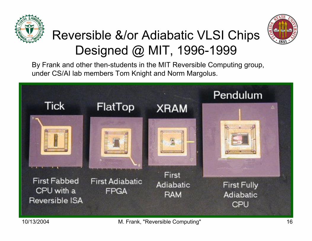
Reversible &/or Adiabatic VLSI Chips
Designed @ MIT, 1996-1999By Frank and other then-students in the MIT Reversible Computing group,
under CS/AI lab members Tom Knight and Norm Margolus.

10/13/2004 M. Frank, "Reversible Computing" 17
Conventional Logic is Irreversible
• Here’s what all of today’s logic gates (including NOT) do continually, i.e., every time their input changes:– They overwrite previous output with a function of their input.
– Performs many-to-one transformation of local digital state!– ∴ required to dissipate �kT on average, by Landauer principle
– Incurs ½CV2 energy dissipation when the output changes.
Just before
transition:
After
transition:
in out in out
0 0
0 1 0 1
1 0 1 0
1 1
in out
Example:
Static CMOS Inverter:
Inverter transition table:
Even a simple NOT gate, as it’s traditionally implemented!
10/13/2004 M. Frank, "Reversible Computing" 18
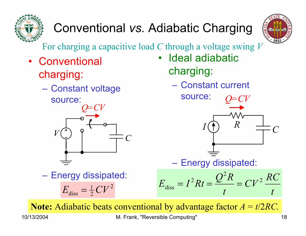
Conventional vs. Adiabatic Charging
• Conventional
charging:
– Constant voltage
source:
– Energy dissipated:
• Ideal adiabatic
charging:
– Constant current
source:
– Energy dissipated:
VC
Q=CV
RCI
Q=CV
t
RCCV
t
RQRtIE 2
22
diss ===2
21
diss CVE =
Note: Adiabatic beats conventional by advantage factor A = t/2RC.
For charging a capacitive load C through a voltage swing V

10/13/2004 M. Frank, "Reversible Computing" 19
Adiabatic Switching with
MOSFETs• Use a voltage ramp to approximate
an ideal current source.
• Switch conditionally,
if MOSFET gate voltage
Vg > V+VT during ramp.
• Can discharge the load later using a similar ramp.
– Either through the same path, or a different path.
t � RC ⇒
t � RC ⇒
t
RCCVE 2
diss →
2
21
diss CVE →
Exact formula:
given speed fraction
s :≡ RC/t
( )[ ] 2/1
diss 11 CVessE s −+= −
Athas ’96, Tzartzanis ‘98

10/13/2004 M. Frank, "Reversible Computing" 20
Requirements for True Adiabatic Logic
in Voltage-coded, FET-based circuits
• Avoid passing current through diodes.– Crossing the “diode drop” leads to irreducible dissipation.
• Follow a “dry switching” discipline (in the relay lingo):– Never turn on a transistor when VDS ≠ 0.
– Never turn off a transistor when IDS ≠ 0.
• Together these rules imply:– The logic design must be logically reversible
• There is no way to erase information under these rules!
– Transitions must be driven by a quasi-trapezoidal waveform
• It must be generated resonantly, with high Q
• Of course, leakage power must also be kept manageable.– Because of this, the optimal design point will not necessarily use the
smallest devices that can ever be manufactured!
• Since the smallest devices may have insoluble problems with leakage.
Important
but often
neglected!
10/13/2004 M. Frank, "Reversible Computing" 21
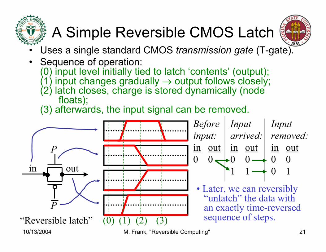
A Simple Reversible CMOS Latch• Uses a single standard CMOS transmission gate (T-gate).
• Sequence of operation:(0) input level initially tied to latch ‘contents’ (output);(1) input changes gradually → output follows closely; (2) latch closes, charge is stored dynamically (node
floats);(3) afterwards, the input signal can be removed.
P
P
in out
Before Input Input
input: arrived: removed:
in out in out in out
0 0 0 0 0 0
1 1 0 1
(0) (1) (2) (3)
• Later, we can reversibly“unlatch” the data withan exactly time-reversedsequence of steps.“Reversible latch”
10/13/2004 M. Frank, "Reversible Computing" 22
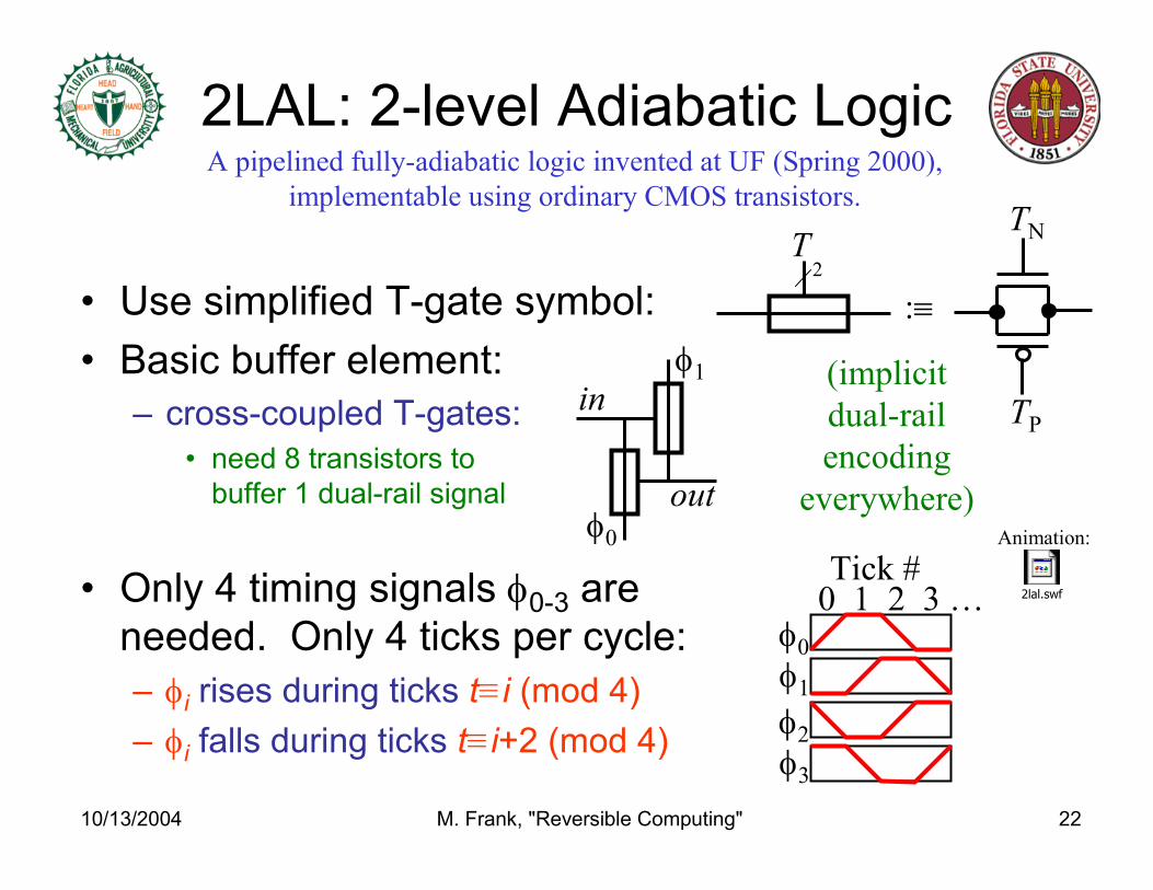
2LAL: 2-level Adiabatic Logic
• Use simplified T-gate symbol:
• Basic buffer element:
– cross-coupled T-gates:
• need 8 transistors to
buffer 1 dual-rail signal
• Only 4 timing signals φ0-3 are
needed. Only 4 ticks per cycle:
– φi rises during ticks t≡i (mod 4)
– φi falls during ticks t≡i+2 (mod 4)
TN
TP
T
:≡
in
out
φ1
φ0
0 1 2 3 …Tick #
φ0
φ1
φ2
φ3
A pipelined fully-adiabatic logic invented at UF (Spring 2000),
implementable using ordinary CMOS transistors.
2
(implicit
dual-rail
encoding
everywhere)
2lal.swf
Animation:

10/13/2004 M. Frank, "Reversible Computing" 23
2LAL Shift Register Structure
in@0
φ1
φ0
φ2
φ1
φ3
φ2
out@4
φ0
φ3
inN
inP
0 1 2 3 ... 0 1 2 3 ...
2lal.swf
Animation:• 1-tick delay per logic stage:
• Logic pulse timing and signal
propagation:
10/13/2004 M. Frank, "Reversible Computing" 24
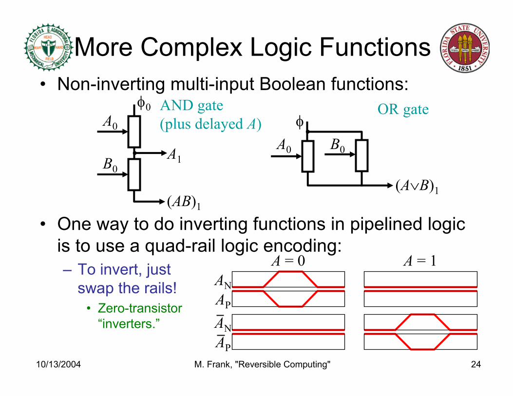
More Complex Logic Functions
• Non-inverting multi-input Boolean functions:
• One way to do inverting functions in pipelined logic
is to use a quad-rail logic encoding:
– To invert, just
swap the rails!
• Zero-transistor
“inverters.”
A0
B0
φ0
A1
(AB)1
A0 B0
φ
(A∨B)1
AN
AP
AN
AP
A = 0 A = 1
AND gate
(plus delayed A)OR gate

10/13/2004 M. Frank, "Reversible Computing" 25
Power vs. freq., TSMC 0.18, Std. CMOS vs. 2LAL
1.E-14
1.E-13
1.E-12
1.E-11
1.E-10
1.E-09
1.E-08
1.E-07
1.E-06
1.E-05
1.E+031.E+041.E+051.E+061.E+071.E+081.E+09
Frequency, Hz
Average power dissipation per nFET, W
Simulation Results from CadenceAssumptions & caveats:
•Assumes ideal trapezoidal
power/clock waveform.
• Minimum-sized devices, 2λ×3λ
* .18 µm (L) × .24 µm (W)
• nFET data is shown
* pFETs data is very similar
• Various body biases tried
* Higher Vth suppresses leakage
• Room temperature operation.
• Interconnect parasitics have not
yet been included.
• Activity factor (transitions per
device-cycle) is 1 for CMOS,
0.5 for 2LAL in this graph.
• Hardware overhead from fully-
adiabatic design style is not
yet reflected
* ≥2× transistor-tick hardware
overhead in known reversible
CMOS design styles
1 nJ
100 pJ10 pJ
1 pJ
100 fJ
10 fJ
1 fJ
100 aJ
10 aJ
1 aJ
100 zJ10 zJ
1 zJ
kTln
2
1 eV
StandardCMOS
2V
1V
0.5V0.25V
2LA
L 1.8-2.0V
Energ
y d
issip
ate
d p
er n
FE
Tper c
ycle
>100× faster
@ 1 pW/T
<.0
1×
the p
ow
er
@ 1
MH
z
100 yJ

10/13/2004 M. Frank, "Reversible Computing" 26
O(log n)-time carry-skip adder
(8 bit segment shown)
Pms Gls Pls
CinGCout
P
P
Pms Gls Pls
CinGCout
P
MS LS
LS
Pms Gls Pls
G
Pms Gls Pls
G
P
P
Pms Gls Pls
CinGCout
P
MS LS
MS
Pms Gls Pls
G
Pms Gls Pls
CinGCout
P
LS
GCoutCin
S A B
P
G Cin
S A B
P
GCoutCin
S A B
P
S A B
P
GCoutCin
S A B
P
S A B
P
GCoutCin
S A B
P
S A B
P
G CinG Cin
G Cin
With this structure, we can do a
2n-bit add in 2(n+1) logic levels
→ 4(n+1) reversible ticks
→ n+1 clock cycles.
Hardware
overhead is
<2× regular
ripple-carry.
1st ca
rry ti
ck
2nd carry tick3rd carry tick4th carry tick

10/13/2004 M. Frank, "Reversible Computing" 27
32-bit Adder Simulation
Results32-bit adder power vs.
frequency
1.E-10
1.E-09
1.E-08
1.E-07
1.E-06
1.E-05
1.E-04
1.E+041.E+051.E+061.E+071.E+08
Add Frequency (Hz)
Power (W)
CMOS pwr
Adia. pwr
32-bit adder energy vs.
frequency
1.E-15
1.E-14
1.E-13
1.E-12
1.E-11
1.E+041.E+051.E+061.E+071.E+08
Add Frequency (Hz)
Energy/Add (J)
CMOS energy
Adia. enrgy
1V CMOS
0.5V CMOS
1V CMOS
0.5V CMOS
2V 2L
AL
, Vsb =
1V
2V 2LA
L, Vsb =1V
(All results normalized to a
throughput level of 1 add/cycle)
20x better perf.@ 3 nW/adder
10/13/2004 M. Frank, "Reversible Computing" 28
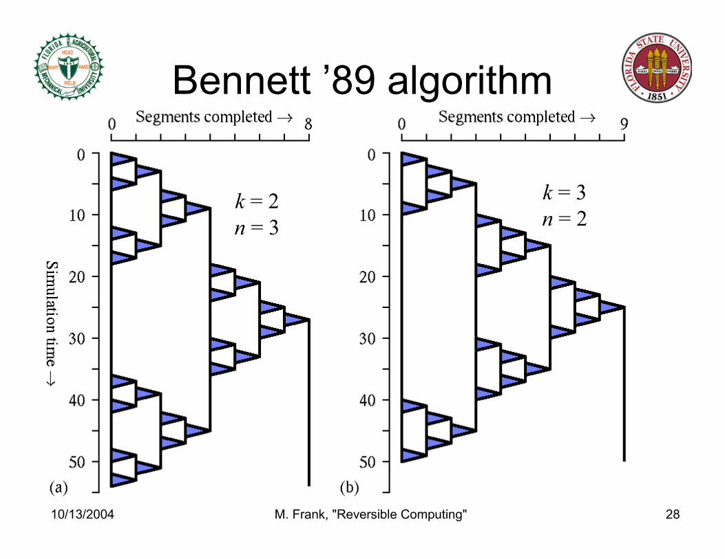
Bennett ’89 algorithm
k = 2
n = 3
k = 3
n = 2

10/13/2004 M. Frank, "Reversible Computing" 29
There’s plenty
of Room for
device improvement…
• Recall, irreversible device technology has at most ~3-4 orders of magnitude of power-performance improvements remaining.– And then, the firm kT ln 2 limit
is encountered.
• But, a wide variety of proposed reversible device technologies have been analyzed by physicists.– With theoretical power-
performance up to 10-12 orders of magnitude better than today’s CMOS!
• Ultimate limits are unclear. 1.E-31
1.E-30
1.E-29
1.E-28
1.E-27
1.E-26
1.E-25
1.E-24
1.E-23
1.E-22
1.E-21
1.E-20
1.E-19
1.E-18
1.E-17
1.E-16
1.E-15
1.E-14
1.E-13
1.E-12
1.E-11
1.E-10
1.E-09
1.E-08
1.E-07
1.E-06
1.E-05
1.E-04
1.E-03
1.E+031.E+041.E+051.E+061.E+071.E+081.E+091.E+101.E+111.E+12
Frequency (Hz)
Power per device (W)
.18um 2LAL
nSQUID
QCA cell
Quantum FET
Rod logic
Param. quantron
Helical logic
.18um CMOS
kT ln 2
.18µm CMOS
.18µm 2L
AL
k(300 K) ln 2
Various
reversible
device proposals
Power per device, vs. frequency
10/13/2004 M. Frank, "Reversible Computing" 30
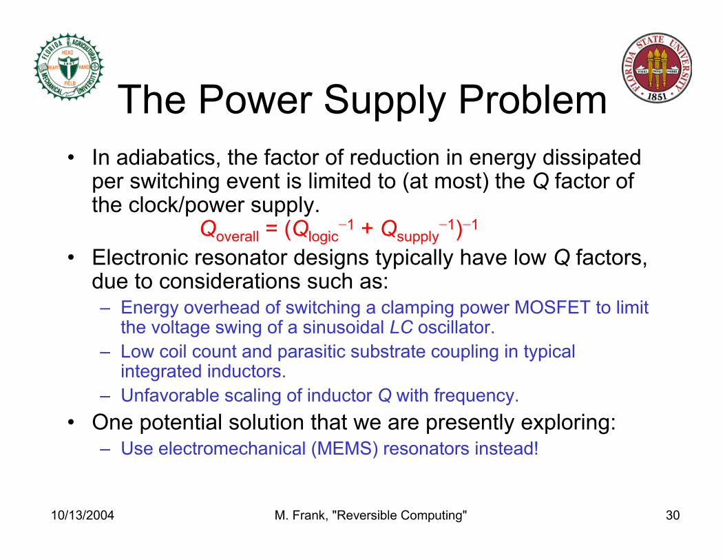
The Power Supply Problem
• In adiabatics, the factor of reduction in energy dissipated per switching event is limited to (at most) the Q factor of the clock/power supply.
Qoverall = (Qlogic−1 + Qsupply
−1)−1
• Electronic resonator designs typically have low Q factors, due to considerations such as:– Energy overhead of switching a clamping power MOSFET to limit
the voltage swing of a sinusoidal LC oscillator.
– Low coil count and parasitic substrate coupling in typical integrated inductors.
– Unfavorable scaling of inductor Q with frequency.
• One potential solution that we are presently exploring: – Use electromechanical (MEMS) resonators instead!
10/13/2004 M. Frank, "Reversible Computing" 31
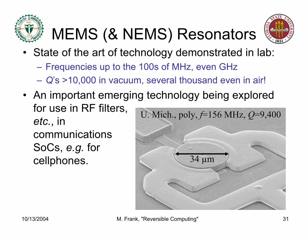
MEMS (& NEMS) Resonators• State of the art of technology demonstrated in lab:
– Frequencies up to the 100s of MHz, even GHz
– Q’s >10,000 in vacuum, several thousand even in air!
• An important emerging technology being explored
for use in RF filters,
etc., in
communications
SoCs, e.g. for
cellphones.
U. Mich., poly, U. Mich., poly, ff=156 MHz, =156 MHz, QQ=9,400=9,400
34 µm

10/13/2004 M. Frank, "Reversible Computing" 32
Original Concept• Imagine a set of charged plates whose horizontal position oscillates
between two sets of interdigitated fixed plates.– Structure forms a variable capacitor and voltage divider with the load.
• Capacitance changes substantially only when crossing border.– Produces nearly flat-topped (quasi-trapezoidal) output waveforms.
– The two output signals have opposite phases (2 of the 4 φ’s in 2LAL)
Logic
load #1
CL
RL
V1
Logic
load #2
CL
RL
t
V1
t
V2
t
V2
x

acv−
acvcV
bV
cV
bcp VVV −=
Actuator
Actuator
Sensor
Sensor
Sensor
Sensor
acvcV
aCsC
rC
bVResonator SchematicUF CONFIDENTIAL – PATENT PENDING
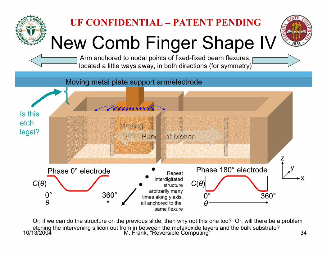
10/13/2004 M. Frank, "Reversible Computing" 34
Moving
plate
Moving metal plate support arm/electrode
New Comb Finger Shape IV
Range of Motion
Arm anchored to nodal points of fixed-fixed beam flexures,
located a little ways away, in both directions (for symmetry)
Phase 0° electrode Phase 180° electrode
θ0° 360°
C(θ) C(θ)
θ0° 360°
Or, if we can do the structure on the previous slide, then why not this one too? Or, will there be a problem
etching the intervening silicon out from in between the metal/oxide layers and the bulk substrate?
…
Repeat
interdigitated
structure
arbitrarily many
times along y axis,
all anchored to the
same flexure
x
y
z
Is this
etch
legal?
UF CONFIDENTIAL – PATENT PENDING

10/13/2004 M. Frank, "Reversible Computing" 35
UF CONFIDENTIAL – PATENT PENDING
Another Candidate Layout

10/13/2004 M. Frank, "Reversible Computing" 36
New simulation results
0
1
2
3
4
5
6
7
8
0 1 2 3 4 5 6 7 8 9
0
1
2
3
4
5
6
7
8
0 2 4 6 8 10 12
UF CONFIDENTIAL – PATENT PENDING
10/13/2004 M. Frank, "Reversible Computing" 37
Serpentine spring
Comb drive
Proof mass
Front-side view
Back-side view
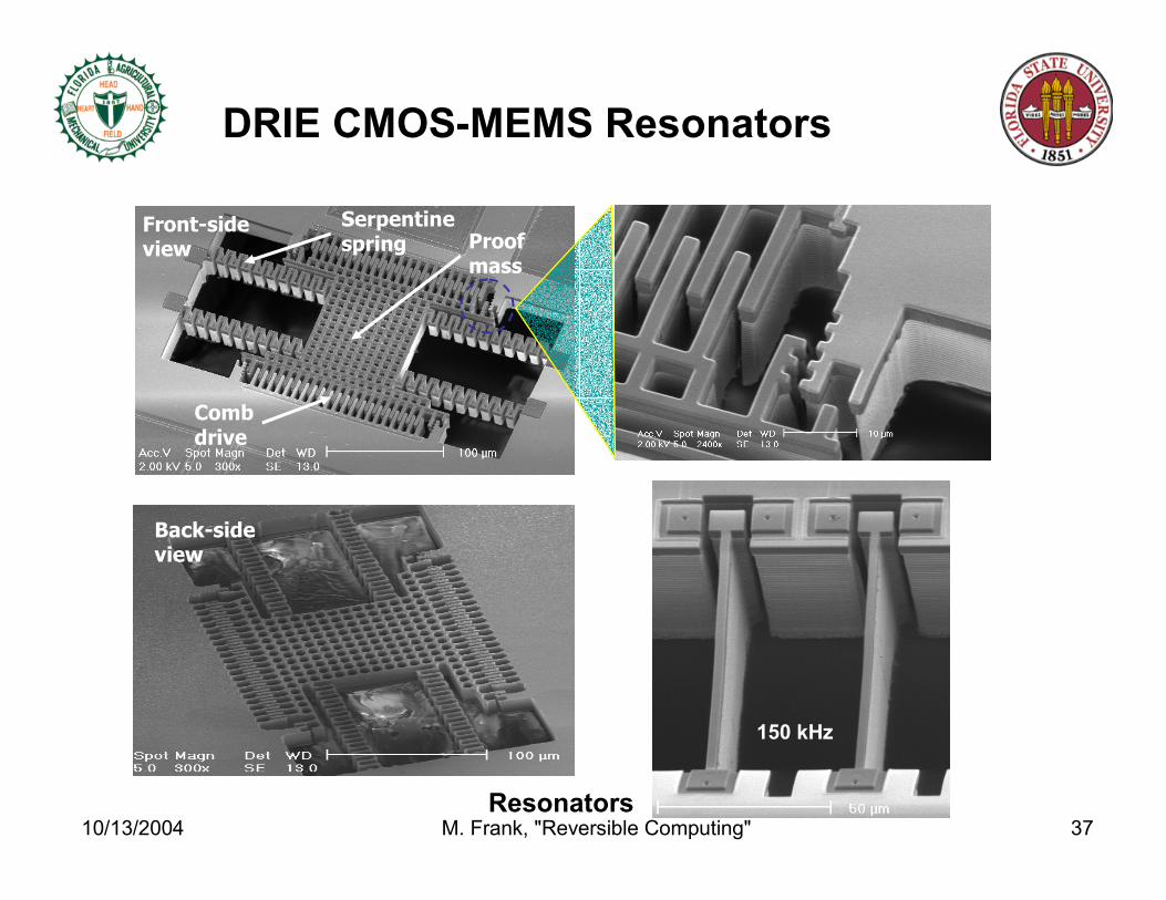
DRIE CMOS-MEMS Resonators
Resonators
150 kHz
10/13/2004 M. Frank, "Reversible Computing" 38
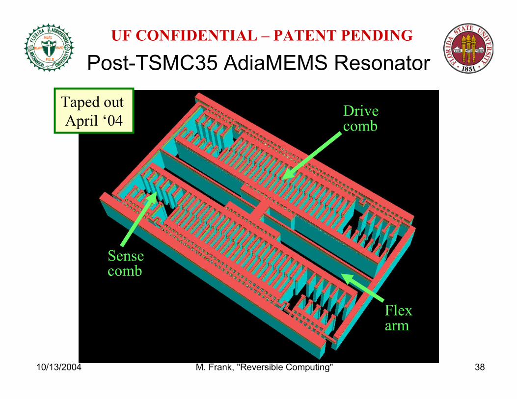
Post-TSMC35 AdiaMEMS Resonator
UF CONFIDENTIAL – PATENT PENDING
Drivecomb
Flexarm
Sensecomb
Taped out
April ‘04

10/13/2004 M. Frank, "Reversible Computing" 39
One Potential Scaling Scenario for Reversible Computing Technology
• Assume energy coefficient (energy diss. / freq.) of reversible technology continues declining at historical rate of 16× / 3 years, through 2020.– For adiabatic CMOS, cE = CV2RC = C2V2R.
• This has been going as ~l4 under constant-field scaling.
– But, requires new devices after CMOS scaling stops.• However, many candidates are waiting in the wings…
• Assume number of affordable layers of active circuitry per chip (or per package, e.g., stacked dies) doubles every 3 years, through 2020.– Competitive pressures will tend to ensure this will
happen, esp. if device-size scaling stops, as assumed.
10/13/2004 M. Frank, "Reversible Computing" 40
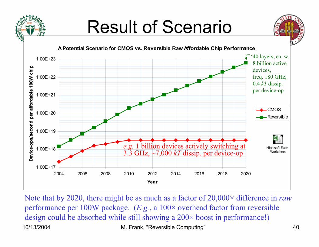
Result of ScenarioA Potential Scenario for CMOS vs. Reversible Raw Affordable Chip Performance
1.00E+17
1.00E+18
1.00E+19
1.00E+20
1.00E+21
1.00E+22
1.00E+23
2004 2006 2008 2010 2012 2014 2016 2018 2020
Year
Device-ops/second per affordable 100W chip
CMOS
Reversible
Note that by 2020, there might be as much as a factor of 20,000× difference in raw
performance per 100W package. (E.g., a 100× overhead factor from reversible
design could be absorbed while still showing a 200× boost in performance!)
40 layers, ea. w.
8 billion active
devices,
freq. 180 GHz,
0.4 kT dissip.
per device-op
Microsoft Excel
Worksheet
e.g. 1 billion devices actively switching at3.3 GHz, ~7,000 kT dissip. per device-op

10/13/2004 M. Frank, "Reversible Computing" 41
Is Reversible Computing
Possible?
• This is a worthwhile question to ask, if:
– By “computing” we mean:• scalable, parallel, general-purpose programmable
digital computation.
– By “reversible computing,” we mean:• computing with <<E energy dissipation per
equivalent irreversible logic operation,– where E is the typical minimum logic signal energy
– And if by “Is it possible?” we mean:• Could cost-effective reversible machines be
economically manufactured within 20-30 years,– Given a sufficient near-term investment in the enabling
basic research?

10/13/2004 M. Frank, "Reversible Computing" 42
Status of this Question
• The absolutely most honest scientific answer is:– No totally confident, definite answer to this question (yes or no)
can be given at present.
• Reversible computing has never been proven to be possible.– For that, we would need a validated empirical demonstration of it
(on top of a demonstrated manufacturing base), or at least a convincingly very complete and clearly buildable physical model.
• Demonstrations have been built, but not competitive ones.
• Physical models have been described, but all are incomplete.
• However, RC has never been proven impossible either.– Doing so would require a rigorous proof from consensus physics
that somehow addresses all physically possible mechanisms.• Various supposed “impossibility” arguments have been offered, but
all of them have been riddled with holes and logical fallacies.

10/13/2004 M. Frank, "Reversible Computing" 43
Some Important Next Steps• Construct a complete quantum mechanical model of a set of high-
quality building blocks for reversible computers.– Some requirements for these devices:
• Include a universal set of reversible and irreversible logic ops
• Extremely low energy coefficient (high Q factor at high frequency)
• Self-contained (time-independent Hamiltonian, no external drivers)
• Scalably composable (in 2D and 3D interconnected networks of devices)
• High reliability (low prob. of soft errors in typical operating environments)
• Self-synchronizing, at least locally (asychronous OK between large blocks)
• Physically realizable Hamiltonian (local, and composable from available physical interactions)
• Run detailed and complete physical simulations of complex digital applications composed of the above building blocks.– Validate that unforeseen problems do not arise at higher design levels.
• Show how to implement these building blocks in an economically viable (cost-effective) manufacturing process.– Show that the resulting systems would operate in a cost-effective
fashion, competitively against conventional designs.
• Migrate supporting tools for new & legacy languages & applications to the new mostly-reversible architectural platforms.

10/13/2004 M. Frank, "Reversible Computing" 44
Conclusion
• Reversible computing is possible…– As far as fundamental physics can tell us at the
moment.
• It is necessary…– To prevent computer performance from stalling within
the next 1-3 decades.
• It is technologically challenging…– A number of research & engineering problems remain
to be solved in order to implement it efficiently…
• We need to aggressively push to solve the remaining problems!– In order for reversible computing to be available in
time to help us achieve extreme supercomputing within the scope of our careers.