retention of resistance states in ferroelectric tunnel...
TRANSCRIPT

Retention of resistance states in ferroelectric tunnel memristorsD. J. Kim, H. Lu, S. Ryu, S. Lee, C. W. Bark, C. B. Eom, and A. Gruverman Citation: Applied Physics Letters 103, 142908 (2013); doi: 10.1063/1.4823989 View online: http://dx.doi.org/10.1063/1.4823989 View Table of Contents: http://scitation.aip.org/content/aip/journal/apl/103/14?ver=pdfcov Published by the AIP Publishing Articles you may be interested in Memristive behaviors in Pt/BaTiO3/Nb:SrTiO3 ferroelectric tunnel junctions Appl. Phys. Lett. 105, 052910 (2014); 10.1063/1.4892846 Resistive switching characteristics in dielectric/ferroelectric composite devices improved by post-thermalannealing at relatively low temperature Appl. Phys. Lett. 104, 092903 (2014); 10.1063/1.4867260 Write operation study of Co/BTO/LSMO ferroelectric tunnel junction J. Appl. Phys. 114, 044108 (2013); 10.1063/1.4816474 Nanoscale electroresistance properties of all-oxide magneto-electric tunnel junction with ultra-thin barium titanatebarrier Appl. Phys. Lett. 102, 052908 (2013); 10.1063/1.4791699 Improvement in retention time of metal–ferroelectric–metal– insulator–semiconductor structures using MgOdoped Ba 0.7 Sr 0.3 TiO 3 insulator layer Appl. Phys. Lett. 83, 981 (2003); 10.1063/1.1597412
This article is copyrighted as indicated in the article. Reuse of AIP content is subject to the terms at: http://scitation.aip.org/termsconditions. Downloaded to IP:
128.104.194.31 On: Mon, 13 Jul 2015 18:20:38

Retention of resistance states in ferroelectric tunnel memristors
D. J. Kim,1 H. Lu,1 S. Ryu,2 S. Lee,2 C. W. Bark,2 C. B. Eom,2 and A. Gruverman1
1Department of Physics and Astronomy & Nebraska Center for Materials and Nanoscience,University of Nebraska, Lincoln, Nebraska 68588, USA2Department of Materials Science and Engineering, University of Wisconsin-Madison, Madison,Wisconsin 53706, USA
(Received 16 March 2013; accepted 17 September 2013; published online 2 October 2013)
Resistive properties of Co/BaTiO3/La2/3Sr1/3MnO3 ferroelectric tunnel junctions on (110) NdGaO3
substrates are investigated. A notable characteristic of these junctions is the memristive behavior—
a dependence of resistance on amplitude and duration of a writing pulse, which is attributed to
field-induced charge accumulation at the Co/BaTiO3 interface. It is found that retention of the
resistance states depends on the thickness of the ferroelectric barrier: the junctions with the thinnest
4-unit-cell-thick BaTiO3 barrier exhibit significant relaxation of the low resistance state while the
junctions with thicker barriers exhibit stable resistance. It is proposed that, in a thinner barrier, a
larger depolarizing field triggers a faster dissipation of the accumulated charges, resulting in a
recovery of interfacial tunnel barrier height and gradual transition from a low to a high resistance
state. VC 2013 AIP Publishing LLC. [http://dx.doi.org/10.1063/1.4823989]
A memristor (an abbreviation of “memory resistor”) was
predicted in 1971 as a fourth fundamental circuit element, in
company with a resistor, an inductor, and a capacitor.1 The
memristor is characterized by the relationship between elec-
tric charge q and magnetic flux u: Du¼MDq, where M is
memristance—a physical coefficient analogous to the resist-
ance between voltage and current. The time derivative of this
equation establishes the relation between voltage and current
illustrating that M is the same as resistance in Ohm’s law
except that M at any time depends on the entire past history
of current.1,2 M is a function of the time integral of the current
flowing through the memristor: it increases continuously with
a current flow and decreases with a reversed current flow.
With no current, M stays constant, e.g., the memristor
remembers its last resistance state. Integrated circuits includ-
ing memristors and memristive systems have the potential to
significantly extend circuit functionality in some applications
such as ultrahigh-dense, nonvolatile memories with the con-
sumption of less power and learning networks that require a
synapse-like function.3–5
Recently, Strukov et al. presented an example of a mem-
ristive device made of a TiO2 layer sandwiched between top
and bottom Pt electrodes.6 In this device, coupled migration
of electrons and ions within the oxide layer induced by an
external bias results in a continuous change of the total de-
vice resistance with the amount of current flowing through
the device.7 A new class of memristive systems, a ferroelec-
tric tunnel memristor, was reported independently by two
research groups,8,9 who proposed alternative mechanisms of
tunable resistance. The first one considers a correlation
between the tunneling resistance and the volume fraction of
the switched polarization.8 In other words, it is based on a
strong difference in tunneling resistance for two opposite
polarization states.10,11 Another proposed mechanism con-
siders tunable resistance in the situation of the fully switched
polarization and invokes the field-induced charge redistribu-
tion at the interface resulting in the modulation of the inter-
face barrier height.9 A common issue for both mechanisms is
that they infer strong polarization retention in the ultrathin
ferroelectric barrier.
In this paper, we investigate the retention behavior of re-
sistance states in the Co/BaTiO3/La2/3Sr1/3MnO3 (Co/BTO/
LSMO) memristors on (110) NdGaO3 substrates and its de-
pendence on the BTO barrier thickness. It is shown that, in a
long time range (more than 1 h), the thinnest (4-unit-cell-
thick) BTO barrier shows a notable relaxation of the low
resistance state, while the resistance of the junctions with
thicker barrier remains stable. Based on these results, we
propose a possible way to enhance the retention properties of
the ferroelectric memristors.
The Co/BTO/LSMO junctions were fabricated by multi-
target pulsed laser deposition (PLD), sputtering, and photo-
lithography. Epitaxial single-crystalline BTO films and
50-nm-thick LSMO bottom electrodes have been grown by
PLD on (110) NdGaO3 (NGO) substrates with in-situ monitor-
ing of high-pressure reflection high-energy electron diffrac-
tion.12 The BTO barrier thickness was varied from 4 to 7 unit
cells (u.c.), equivalent to the 1.6–2.8 nm thickness range.
Before deposition, a low miscut NGO substrate was treated by
a modified buffered HF etch and annealed in oxygen atmos-
phere to create an atomically smooth surface. 10-nm-thick top
Co electrodes of 5 lm in diameter have been fabricated by
sputtering and photo-lithographic patterning. Gold passivation
layer was deposited onto Co top electrodes to avoid oxidation.
The details of sample preparation can be found elsewhere.9 To
investigate the retention of the resistance states, current-
voltage (I-V) characteristics of the junctions were measured as
a function of a delay time from the application of a writing
pulse of variable amplitude and duration by means of conduc-
tive atomic force microscopy (MFP-3D, Asylum Research)
using boron-doped diamond-coated cantilevers. Tunneling re-
sistance values were determined from a slope of I-V curves
obtained by a linear fitting in a range of 65 mV. The polariza-
tion state of the junctions was tested by means of piezores-
ponse force microscopy (PFM). The pristine samples were
typically in a weakly polarized state.
0003-6951/2013/103(14)/142908/4/$30.00 VC 2013 AIP Publishing LLC103, 142908-1
APPLIED PHYSICS LETTERS 103, 142908 (2013)
This article is copyrighted as indicated in the article. Reuse of AIP content is subject to the terms at: http://scitation.aip.org/termsconditions. Downloaded to IP:
128.104.194.31 On: Mon, 13 Jul 2015 18:20:38
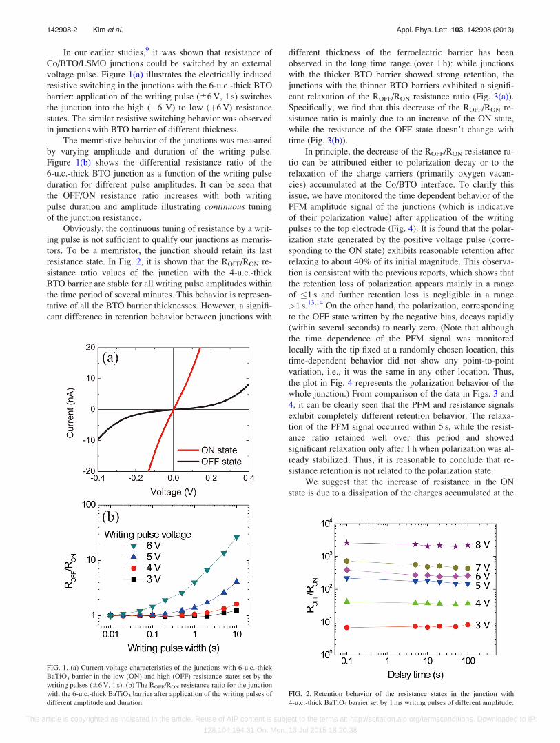
In our earlier studies,9 it was shown that resistance of
Co/BTO/LSMO junctions could be switched by an external
voltage pulse. Figure 1(a) illustrates the electrically induced
resistive switching in the junctions with the 6-u.c.-thick BTO
barrier: application of the writing pulse (66 V, 1 s) switches
the junction into the high (�6 V) to low (þ6 V) resistance
states. The similar resistive switching behavior was observed
in junctions with BTO barrier of different thickness.
The memristive behavior of the junctions was measured
by varying amplitude and duration of the writing pulse.
Figure 1(b) shows the differential resistance ratio of the
6-u.c.-thick BTO junction as a function of the writing pulse
duration for different pulse amplitudes. It can be seen that
the OFF/ON resistance ratio increases with both writing
pulse duration and amplitude illustrating continuous tuning
of the junction resistance.
Obviously, the continuous tuning of resistance by a writ-
ing pulse is not sufficient to qualify our junctions as memris-
tors. To be a memristor, the junction should retain its last
resistance state. In Fig. 2, it is shown that the ROFF/RON re-
sistance ratio values of the junction with the 4-u.c.-thick
BTO barrier are stable for all writing pulse amplitudes within
the time period of several minutes. This behavior is represen-
tative of all the BTO barrier thicknesses. However, a signifi-
cant difference in retention behavior between junctions with
different thickness of the ferroelectric barrier has been
observed in the long time range (over 1 h): while junctions
with the thicker BTO barrier showed strong retention, the
junctions with the thinner BTO barriers exhibited a signifi-
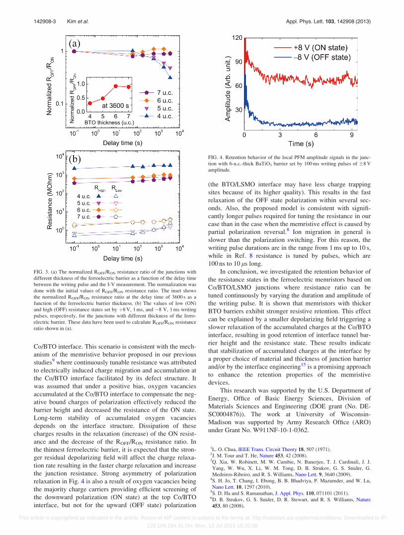
cant relaxation of the ROFF/RON resistance ratio (Fig. 3(a)).
Specifically, we find that this decrease of the ROFF/RON re-
sistance ratio is mainly due to an increase of the ON state,
while the resistance of the OFF state doesn’t change with
time (Fig. 3(b)).
In principle, the decrease of the ROFF/RON resistance ra-
tio can be attributed either to polarization decay or to the
relaxation of the charge carriers (primarily oxygen vacan-
cies) accumulated at the Co/BTO interface. To clarify this
issue, we have monitored the time dependent behavior of the
PFM amplitude signal of the junctions (which is indicative
of their polarization value) after application of the writing
pulses to the top electrode (Fig. 4). It is found that the polar-
ization state generated by the positive voltage pulse (corre-
sponding to the ON state) exhibits reasonable retention after
relaxing to about 40% of its initial magnitude. This observa-
tion is consistent with the previous reports, which shows that
the retention loss of polarization appears mainly in a range
of �1 s and further retention loss is negligible in a range
>1 s.13,14 On the other hand, the polarization, corresponding
to the OFF state written by the negative bias, decays rapidly
(within several seconds) to nearly zero. (Note that although
the time dependence of the PFM signal was monitored
locally with the tip fixed at a randomly chosen location, this
time-dependent behavior did not show any point-to-point
variation, i.e., it was the same in any other location. Thus,
the plot in Fig. 4 represents the polarization behavior of the
whole junction.) From comparison of the data in Figs. 3 and
4, it can be clearly seen that the PFM and resistance signals
exhibit completely different retention behavior. The relaxa-
tion of the PFM signal occurred within 5 s, while the resist-
ance ratio retained well over this period and showed
significant relaxation only after 1 h when polarization was al-
ready stabilized. Thus, it is reasonable to conclude that re-
sistance retention is not related to the polarization state.
We suggest that the increase of resistance in the ON
state is due to a dissipation of the charges accumulated at the
FIG. 1. (a) Current-voltage characteristics of the junctions with 6-u.c.-thick
BaTiO3 barrier in the low (ON) and high (OFF) resistance states set by the
writing pulses (66 V, 1 s). (b) The ROFF/RON resistance ratio for the junction
with the 6-u.c.-thick BaTiO3 barrier after application of the writing pulses of
different amplitude and duration.
FIG. 2. Retention behavior of the resistance states in the junction with
4-u.c.-thick BaTiO3 barrier set by 1 ms writing pulses of different amplitude.
142908-2 Kim et al. Appl. Phys. Lett. 103, 142908 (2013)
This article is copyrighted as indicated in the article. Reuse of AIP content is subject to the terms at: http://scitation.aip.org/termsconditions. Downloaded to IP:
128.104.194.31 On: Mon, 13 Jul 2015 18:20:38
Co/BTO interface. This scenario is consistent with the mech-
anism of the memristive behavior proposed in our previous
studies9 where continuously tunable resistance was attributed
to electrically induced charge migration and accumulation at
the Co/BTO interface facilitated by its defect structure. It
was assumed that under a positive bias, oxygen vacancies
accumulated at the Co/BTO interface to compensate the neg-
ative bound charges of polarization effectively reduced the
barrier height and decreased the resistance of the ON state.
Long-term stability of accumulated oxygen vacancies
depends on the interface structure. Dissipation of these
charges results in the relaxation (increase) of the ON resist-
ance and the decrease of the ROFF/RON resistance ratio. In
the thinnest ferroelectric barrier, it is expected that the stron-
ger residual depolarizing field will affect the charge relaxa-
tion rate resulting in the faster charge relaxation and increase
the junction resistance. Strong asymmetry of polarization
relaxation in Fig. 4 is also a result of oxygen vacancies being
the majority charge carriers providing efficient screening of
the downward polarization (ON state) at the top Co/BTO
interface, but not for the upward (OFF state) polarization
(the BTO/LSMO interface may have less charge trapping
sites because of its higher quality). This results in the fast
relaxation of the OFF state polarization within several sec-
onds. Also, the proposed model is consistent with signifi-
cantly longer pulses required for tuning the resistance in our
case than in the case when the memristive effect is caused by
partial polarization reversal.8 Ion migration in general is
slower than the polarization switching. For this reason, the
writing pulse durations are in the range from 1 ms up to 10 s,
while in Ref. 8 resistance is tuned by pulses, which are
100 ns to 10 ls long.
In conclusion, we investigated the retention behavior of
the resistance states in the ferroelectric memristors based on
Co/BTO/LSMO junctions where resistance ratio can be
tuned continuously by varying the duration and amplitude of
the writing pulse. It is shown that memristors with thicker
BTO barriers exhibit stronger resistive retention. This effect
can be explained by a smaller depolarizing field triggering a
slower relaxation of the accumulated charges at the Co/BTO
interface, resulting in good retention of interface tunnel bar-
rier height and the resistance state. These results indicate
that stabilization of accumulated charges at the interface by
a proper choice of material and thickness of junction barrier
and/or by the interface engineering15 is a promising approach
to enhance the retention properties of the memristive
devices.
This research was supported by the U.S. Department of
Energy, Office of Basic Energy Sciences, Division of
Materials Sciences and Engineering (DOE grant (No. DE-
SC0004876)). The work at University of Wisconsin-
Madison was supported by Army Research Office (ARO)
under Grant No. W911NF-10-1-0362.
1L. O. Chua, IEEE Trans. Circuit Theory 18, 507 (1971).2J. M. Tour and T. He, Nature 453, 42 (2008).3Q. Xia, W. Robinett, M. W. Cumbie, N. Banerjee, T. J. Cardinali, J. J.
Yang, W. Wu, X. Li, W. M. Tong, D. B. Strukov, G. S. Snider, G.
Medeiros-Ribeiro, and R. S. Williams, Nano Lett. 9, 3640 (2009).4S. H. Jo, T. Chang, I. Ebong, B. B. Bhadviya, P. Mazumder, and W. Lu,
Nano Lett. 10, 1297 (2010).5S. D. Ha and S. Ramanathan, J. Appl. Phys. 110, 071101 (2011).6D. B. Strukov, G. S. Snider, D. R. Stewart, and R. S. Williams, Nature
453, 80 (2008).
FIG. 3. (a) The normalized ROFF/RON resistance ratio of the junctions with
different thickness of the ferroelectric barrier as a function of the delay time
between the writing pulse and the I-V measurement. The normalization was
done with the initial values of ROFF/RON resistance ratio. The inset shows
the normalized ROFF/RON resistance ratio at the delay time of 3600 s as a
function of the ferroelectric barrier thickness. (b) The values of low (ON)
and high (OFF) resistance states set by þ8 V, 1 ms, and �8 V, 1 ms writing
pulses, respectively, for the junctions with different thickness of the ferro-
electric barrier. These data have been used to calculate ROFF/RON resistance
ratio shown in (a).
FIG. 4. Retention behavior of the local PFM amplitude signals in the junc-
tion with 6-u.c.-thick BaTiO3 barrier set by 100 ms writing pulses of 68 V
amplitude.
142908-3 Kim et al. Appl. Phys. Lett. 103, 142908 (2013)
This article is copyrighted as indicated in the article. Reuse of AIP content is subject to the terms at: http://scitation.aip.org/termsconditions. Downloaded to IP:
128.104.194.31 On: Mon, 13 Jul 2015 18:20:38

7J. J. Yang, M. D. Pickett, X. Li, D. A. A. Ohlberg, D. R. Stewart, and R. S.
Williams, Nat. Nanotechnol. 3, 429 (2008).8A. Chanthbouala, V. Garcia, R. O. Cherifi, K. Bouzehouane, S. Fusil, X.
Moya, S. Xavier, H. Yamada, C. Deranlot, N. D. Mathur, M. Bibes, A.
Barth�el�emy, and J. Grollier, Nature Mater. 11, 860 (2012).9D. J. Kim, H. Lu, S. Ryu, C.-W. Bark, C.-B. Eom, E. Y. Tsymbal, and A.
Gruverman, Nano Lett. 12, 5697 (2012).10A. Gruverman, D. Wu, H. Lu, Y. Wang, H. W. Jang, C. M. Folkman, M.
Y. Zhuravlev, D. Felker, M. Rzchowski, C.-B. Eom, and E. Y. Tsymbal,
Nano Lett. 9, 3539 (2009).11V. Garcia, S. Fusil, K. Bouzehouane, S. Enouz-Vedrenne, N. D. Mathur,
A. Barth�el�emy, and M. Bibes, Nature 460, 81 (2009).
12K. J. Choi, M. Biegalski, Y. L. Li, A. Sharan, J. Schubert, R. Uecker, P.
Reiche, Y. B. Chen, X. Q. Pan, V. Gopalan, L.-Q. Chen, D. G. Schlom,
and C. B. Eom, Science 306, 1005 (2004).13D. J. Kim, J. Y. Jo, Y. W. So, B. S. Kang, T. W. Noh, J.-G. Yoon, T. K.
Song, K. H. Noh, S.-S. Lee, S.-H. Oh, K.-N. Lee, S.-K. Hong, and Y.-J.
Park, Appl. Phys. Lett. 86, 022903 (2005).14D. J. Kim, J. Y. Jo, Y. S. Kim, Y. J. Chang, J. S. Lee, J.-G. Yoon, T. K.
Song, and T. W. Noh, Phys. Rev. Lett. 95, 237602 (2005).15H. Lu, X. Liu, J. D. Burton, C.-W. Bark, Y. Wang, Y. Zhang, D. J. Kim,
A. Stamm, P. Lukashev, D. A. Felker, C. M. Folkman, P. Gao, M. S.
Rzchowski, X. Q. Pan, C.-B. Eom, E. Y. Tsymbal, and A. Gruverman,
Adv. Mater. 24, 1209 (2012).
142908-4 Kim et al. Appl. Phys. Lett. 103, 142908 (2013)
This article is copyrighted as indicated in the article. Reuse of AIP content is subject to the terms at: http://scitation.aip.org/termsconditions. Downloaded to IP:
128.104.194.31 On: Mon, 13 Jul 2015 18:20:38