resolution circle tech...
TRANSCRIPT

Resolution Circle
Tech Stations

Our Tech Stations infrastructure is designed to provide commercial prototyping services, including small-scale manufacturing. The philosophy is one of “idea-to-barcode” – a horizontally integrated ecosystem where innovation can come to life in prototypes and small-scale manufacturing. Some of the dedicated technology areas housed in
the 7500sqm Resolution Circle Towers are the following:
overview
3D Printing3D Printing
Chemistry Lab
CAD
Electro-magnetic
Interference
NDT PCB
Composite Materials
HALT&
HASS
3-D printing is an additive manufacturing method used to rapidly produce three- dimensional objects. Some applications include 3-Dprinted prosthetics, dental moulds, art, tooling and general research.
Resolution Circle’s 3-D printing Tech Station contributes to a critical part of the research and development department, as it is utilised for rapid prototyping when a product under development needs to be evaluated for functionality, assembly and aesthetics.
The basic process flow to perform 3-D printing is to firstly draw a 3-D CAD model of the part to be created, to export the model to the 3-D printer’s software, to interpret the model and generate the corresponding machine toolpaths and finally to print the part.
Post-manufacturing finishing of printed components is often required, including processes such as removal of support materials and light sanding.
3D Printing3D Printing
Lab capabilities Desktop 3D-PrintersThese printers are used as a means for fast and cost effective print models. They are fairly accurate and relatively low in price, but offer a small print size. The material capabilities include ABS, PLA and Nylon. This type of printing is most suitable for parts that require simple geometry and where accurate tolerance are not essential.
Fortus 400MCThis a professional Fused Deposition Modelling (FDM) printer. The parts produced by this printer are strong, highly accurate and can be used as functional parts - bearing in mind that it will be made out of plastic. The material capabilities of this printer include ABS, Nylon and Ultem (structural material).
MCor IrisThis full colour 3D-printer is best suited for slightly larger models that can be produced out of paper, although the models produced cannot be used as functional parts. The main application area of this printer are marketing, art, landscapes and architectural models.
Envisiontech printerThis printer uses stereolithographic technology to produce extremely accurate 3-D prints. It is most suitable for parts that need to be dimensionally accurate with an excellent surface finish such as dental moulds. The material capabilities of this printer include HTM140 V2 (a liquid plastic that hardens when it’s placed under an ultra violet light).
The chemistry laboratory at Resolution Circle is a multi-purpose facility that plays an important role in a number of product development processes as well as quality control and substance detection, for both inventors and industry.
A few noteworthy capabilities include:
Process modelling - complicated chemical processes and reactions may be accurately modelled in software to obtain predictions regarding process performance. This allows for process engineering endeavours that do without the costs of traditional lab-based experiments. In addition to this, the software-based process modelling may be used as a precursor to real-world tests, such that the modelling ensures that only the most feasible method is selected before doing the more costly pilot-scale experiments. Software modelling may also be required when up-scaling to ensure that the trials scale well.
Nano-technology as related to developing new chemical sensors – we are able to create the magnetic carriers required to carry the substance sensors. In addition to this, we are able to create a turnkey substance detection system using these magnetic separators or to provide them as a tool for further research.
Model validation through physical experimentation – software-based modelling has its limitations and eventually pilot-scale physical experimentation will be required to validate the modelling results. This is also important if the real-world production performance does not match the model predicted outcomes. We perform demonstrable reaction-based chemistry.
Applied commercial research and development – here we place an emphasis on the development part of the product design cycle. Through meticulous procedures and time-tested development principles that drive innovation, we are able to perform chemistry related product development with a focus on generation and protection of intellectual property.
Process development – we are able to develop new chemical processes from scratch, or refine, optimise and expand on existing processes. With rising economic pressure and increasingly competitive markets, companies are forced to rethink their process strategies and we can assist with that. We cater for both small and industrial scale process design and optimisation.
Reverse engineering – either due to lost documentation or lost access to skills and people, it may be necessary to reverse engineer, or re-engineer, a process or product.
The chemistry lab maintains a world-class environment in which product and process development may occur, whilst both honouring and facilitating intellectual property generation and protection as well as technology transfer.
Chemistry Lab

Our composite materials technology station’s primary function is to manufacture composite products from hybrid materials such as fiber glass and carbon fiber. These products can vary in size and shape and are accurately manufactured using CNC machining and CAD design technology.
Lab Capabilities Components manufactured from composite materials Vacuum bagging hand lay ups Resin infusion Post curing Pre-impregnated materials Mold manufacturing CNC Routing
Composite material is classified as two or more fundamental materials engineered into a single body with different physical or chemical properties. The different materials remain separate and distinct within the final structure at a macroscopic level, but they complement one another in order to create the desired composite material properties.
Composite materials are mostly used for their favourable features such as light weight, good fatigue resistance, corrosion resistance, comparatively low price and shape complexity.
Unique moulds for the composite materials may be manufactured either by CNC-machining the entire mould directly out of the desired material (wood or polystyrene) or CNC-machining a plug for moulding purposes, which adds split line capabilities to the moulds.
Computer Aided Design (CAD) is software that enables the design of three-dimensional objects in various digital formats, which allows designers and engineers to construct and evaluate designs in virtual reality before production.
The primary advantages of CAD in the design process are increased flexibility and time efficiency.
Resolution Circle’s CAD-station consists of 10 high-performance CAD workstation computers, especially equipped with features to accommodate the requirements of advanced resource-hungry software.
Lab Capabilities
MechanicalA complete up-to-date commercial mechanical CAD software package is available which facilitates a digital design process including modelling, Finite Element Analysis, Product Data Management and Nesting functions. These functions enable the client to take a design from conceptualisation through to refinement for manufacturing using one software package.
Architectural SystemsRevit MEP (Mechanical, Electrical and Plumbing) is system design software mainly used for architectural designs. A key feature of Revit is the software’s change management functionality: any design modifications (be it mechanical, electrical or plumbing) will automatically be propagated throughout the entire design to ensure all changes are taken into consideration so they can be properly merged.
ElectronicsAltium Designer and OrCAD are electronic design automation software packages for printed circuit board and embedded software design. Used in conjunction with each other, they provide an efficient workflow for board-level electronics designers as they ensure design success by reducing the overall design times. Functions include: schematic capture, printed circuit board layout design, 3D modelling and output generation for final manufacturing.
CAD Composite Materials
As part of Resolution Circle’s offering to provide a complete electronic design solution of taking an idea and turning it into a production ready product, compliance testing of certain regulatory standards are offered. One such regulatory standard involves limits prescribing the electromagnetic interference (EMI) generated by a product as well as the products susceptibility to externally generated EMI.
Electromagnetic Compatibility (EMC) is defined as the ability of a device to operate in the electromagnetic environment without affecting other devices negatively, whilst at the same time being unaffected by the operation of other devices.
EMC has become a necessity for commercial electrical and electronic devices. Resolution Circle aims to assist the design process by providing pre-compliance EMC testing to designers throughout the development process. This reduces the risk of a finished product failing EMC compliance testing, which can be costly and time consuming and delays the development time to achieve a market ready product.
Lab CapabilitiesResolution circle has the capability of doing pre-compliance testing in the following areas:
Conducted Susceptibility: measuring the ability of a device to withstand EMI present on the mains distribution network.
Conducted Emissions: measuring the extent to which the device emits EMI into the mains distribution network.
Radiated Susceptibility: measuring the ability of a device to withstand radiated EMI present in the operating environment of the device.
Radiated Emissions: measuring the extent to which the device radiates EMI into the environment.
Resolution Circle has an electromagnetically isolated test chamber (GTEM) which allows for the above described radiated emission and susceptibility tests to be performed without the need for an anechoic chamber.
HALT**Highly Accelerated Life Testing
During the HALT process, a product is subjected to increasing stress levels of temperature and vibration (independently and in combination).
The HALT technology station at Resolution Circle is used to perform Highly Accelerated Life Tests on newly developed products smaller than 400x400x250mm utilising temperature variation between -40 and 200 degrees Celsius while vibrating the product up to 100gRMS.
Interpreting the results of a HALT provides one with knowledge of typically expected failure rates, expected mechanical breakages and the product toughness.
HASS****Highly Accelerated Stress Screening
In addition to the HALT one can perform Highly Accelerated Stress Screening on statistically selected products during manufacturing to confirm the product compliance to the expected standard.
HALT and HASS are often utilised in conjunction for superior testing results
Electro-magnetic
Interference
HALT&
HASS
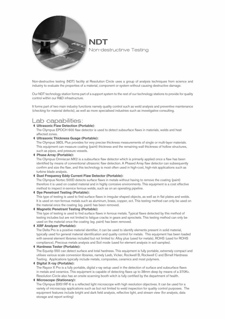
Non-destructive testing (NDT) facility at Resolution Circle uses a group of analysis techniques from science and industry to evaluate the properties of a material, component or system without causing destructive damage.
Our NDT technology station forms part of a support system to the rest of our technology stations to provide for quality control within our R&D infrastructure.
It forms part of two main industry functions namely quality control such as weld analysis and preventive maintenance (checking for material defects), as well as more specialised industries such as investigative consulting.
Lab capabilities: Ultrasonic Flaw Detection (Portable):The Olympus EPOCH 600 flaw detector is used to detect subsurface flaws in materials, welds and heat affected zones.
Ultrasonic Thickness Guage (Portable):The Olympus 38DL Plus provides for very precise thickness measurements of single or multi-layer materials. This equipment can measure coating (paint) thickness and the remaining wall thickness of hollow structures, such as pipes, and pressure vessels.
Phase Array (Portable):The Olympus Omniscan MX2 is a subsurface flaw detector which is primarily applied once a flaw has been identified by means of conventional ultrasonic flaw detection. A Phased Array flaw detector can subsequently confirm and size the flaw, and this technology is most often used in high-cost, high-risk applications such as turbine blade analysis.
Duel Frequency Eddy Current Flaw Detector (Portable):The Olympus Nortec 500D detects surface flaws in metals without having to remove the coating (paint) therefore it is used on coated material and in highly corrosive environments. This equipment is a cost effective method to inspect in-service ferrous welds, such as on an operating pipeline.
Dye Penetrant Testing (Portable):This type of testing is used to find surface flaws in irregular shaped objects, as well as in flat plates and welds. It is used on non-ferrous metals such as aluminum, brass, copper, ect. This testing method can only be used on the material once the coating (eg. paint) has been removed.
Magnetic Penetrant Testing (Portable):This type of testing is used to find surface flaws in ferrous metals. Typical flaws detected by this method of testing includes but are not limited to fatigue cracks in gears and sprockets. This testing method can only be used on the material once the coating (eg. paint) has been removed.
XRF Analyzer (Portable):The Delta Pro is a positive material identifier, it can be used to identify elements present in solid material, typically used for general material identification and quality control for metals. This equipment has been loaded with several element libraries included but not limited to: Alloy plus (used for metals), ROHS (used for ROHS compliance), Precious metals analysis and Soil mode (used for element analysis in soil samples).
Hardness Tester (Portable):The Equotip 550 can detect surface and total hardness. This equipment is fully portable, extremely compact and utilises various scale conversion libraries, namely Leeb, Vicker, Rockwell B, Rockwell C and Birnell Hardness Testing. Applications typically include metals, composites, ceramics and most polymers.
Digital X-ray (Portable):The Rayzor X Pro is a fully portable, digital x-ray setup used in the detection of surface and subsurface flaws in metals and ceramics. This equipment is capable of detecting flaws up to 38mm deep by means of a 370Kv. Resolution Circle also has an onsite scanning booth witch is fully certified by the department of health.
Microscope (Stationary): The Olympus BX51RF-6 is a reflected light microscope with high resolution objectives. It can be used for a variety of microscopy applications such as but not limited to weld inspection for quality control purposes. The equipment features include bright and dark field analysis, reflective light, and stream view (for analysis, data storage and report writing)
NDTNon-destructinve Testing
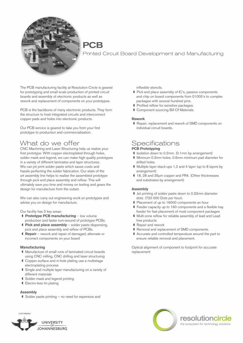
The PCB manufacturing facility at Resolution Circle is geared for prototyping and small scale production of printed circuit boards and assembly of electronic products as well as rework and replacement of components on your prototypes.
PCB is the backbone of many electronic products. They form the structure to host integrated circuits and interconnect copper pads and holes into electronic products.
Our PCB service is geared to take you from your first prototype to production and commercialisation.
What do we offerCNC Machining and Laser Structuring help us realise your first prototype. With copper electroplated through holes, solder mask and legend, we can make high quality prototypes in a variety of different laminates and layer structures. We can jet print solder paste which saves costs and hassle perfecting the solder fabrication. Our state of the art assembly line helps to realise the assembled prototype through pick and place assembly and reflow. This will ultimately save you time and money on testing and gears the design for manufacture from the outset.
We can also carry out engineering work on prototypes and advise you on design for manufacture.
Our facility has 3 key areas: Prototype PCB manufacturing – low volume production and faster turn-around of prototype PCBs.
Pick and place assembly – solder paste dispensing, pick and place assembly and reflow of PCBs.
Repair – rework and repair of damaged, alternate or incorrect components on your board
Manufacturing Manufacture of small runs of laminated circuit boards using CNC milling, CNC drilling and laser structuring
Copper surface and in-hole plating use a multistage electroplating process
Single and multiple layer manufacturing on a variety of different materials
Solder mask and legend printing Electro-less tin plating
Assembly Solder paste printing – no need for expensive and
PCBPrinted Circuit Board Development and Manufacturing
inflexible stencils. Pick and place assembly of IC’s, passive components and chip on board components from 01005’s to complex packages with several hundred pins.
Profiled reflow for sensitive packages. Component sourcing Bill Of Materials.
Rework Repair, replacement and rework of SMD components on individual circuit boards.
SpecificationsPCB Prototyping
Isolation down to 0.2mm. (0.1mm by arrangement) Minimum 0.3mm holes. 0.6mm minimum pad diameter for drilled holes.
Multiple layer stack-ups 1,2 and 4 layer (up to 8 layers by arrangement)
18, 28 and 35µm copper and FR4. (Other thicknesses and substrates by arrangement)
Assembly Jet printing of solder paste down to 0.33mm diameter dots. (720 000 Dots per hour).
Placement of up to 16000 components an hour Feeder capacity up to 160 components and a flexible tray feeder for fast placement of most component packages
Multi-zone reflow for reliable assembly of lead and Lead free products
Repair and rework Removal and replacement of SMD components. Accurate and controlled temperature around the part to ensure reliable removal and placement.
Optical alignment of component to footprint for accurate replacement
www.facebook.com/ResolutionCircle
Jacques VenterHead of Department: Technical Operations
[email protected] | +27 10 020 3760 | +27 84 555 8695
Dr Wiehan le RouxGroup Senior Manager: Research and Development
[email protected] | +27 10 020 3777 | +27 83 709 7931
www.resolutioncircle.co.za www.twitter.com/@res_circlewww.linkedin.com/company/ResolutionCircle